EP4037301A1 - Imaging device and mobile body - Google Patents
Imaging device and mobile body Download PDFInfo
- Publication number
- EP4037301A1 EP4037301A1 EP20870107.8A EP20870107A EP4037301A1 EP 4037301 A1 EP4037301 A1 EP 4037301A1 EP 20870107 A EP20870107 A EP 20870107A EP 4037301 A1 EP4037301 A1 EP 4037301A1
- Authority
- EP
- European Patent Office
- Prior art keywords
- imaging
- imaging device
- elastic member
- optical system
- contact
- Prior art date
- Legal status (The legal status is an assumption and is not a legal conclusion. Google has not performed a legal analysis and makes no representation as to the accuracy of the status listed.)
- Granted
Links
Images



Classifications
-
- G—PHYSICS
- G03—PHOTOGRAPHY; CINEMATOGRAPHY; ANALOGOUS TECHNIQUES USING WAVES OTHER THAN OPTICAL WAVES; ELECTROGRAPHY; HOLOGRAPHY
- G03B—APPARATUS OR ARRANGEMENTS FOR TAKING PHOTOGRAPHS OR FOR PROJECTING OR VIEWING THEM; APPARATUS OR ARRANGEMENTS EMPLOYING ANALOGOUS TECHNIQUES USING WAVES OTHER THAN OPTICAL WAVES; ACCESSORIES THEREFOR
- G03B17/00—Details of cameras or camera bodies; Accessories therefor
- G03B17/02—Bodies
-
- G—PHYSICS
- G03—PHOTOGRAPHY; CINEMATOGRAPHY; ANALOGOUS TECHNIQUES USING WAVES OTHER THAN OPTICAL WAVES; ELECTROGRAPHY; HOLOGRAPHY
- G03B—APPARATUS OR ARRANGEMENTS FOR TAKING PHOTOGRAPHS OR FOR PROJECTING OR VIEWING THEM; APPARATUS OR ARRANGEMENTS EMPLOYING ANALOGOUS TECHNIQUES USING WAVES OTHER THAN OPTICAL WAVES; ACCESSORIES THEREFOR
- G03B11/00—Filters or other obturators specially adapted for photographic purposes
- G03B11/04—Hoods or caps for eliminating unwanted light from lenses, viewfinders or focusing aids
-
- G—PHYSICS
- G03—PHOTOGRAPHY; CINEMATOGRAPHY; ANALOGOUS TECHNIQUES USING WAVES OTHER THAN OPTICAL WAVES; ELECTROGRAPHY; HOLOGRAPHY
- G03B—APPARATUS OR ARRANGEMENTS FOR TAKING PHOTOGRAPHS OR FOR PROJECTING OR VIEWING THEM; APPARATUS OR ARRANGEMENTS EMPLOYING ANALOGOUS TECHNIQUES USING WAVES OTHER THAN OPTICAL WAVES; ACCESSORIES THEREFOR
- G03B17/00—Details of cameras or camera bodies; Accessories therefor
- G03B17/02—Bodies
- G03B17/12—Bodies with means for supporting objectives, supplementary lenses, filters, masks, or turrets
-
- G—PHYSICS
- G03—PHOTOGRAPHY; CINEMATOGRAPHY; ANALOGOUS TECHNIQUES USING WAVES OTHER THAN OPTICAL WAVES; ELECTROGRAPHY; HOLOGRAPHY
- G03B—APPARATUS OR ARRANGEMENTS FOR TAKING PHOTOGRAPHS OR FOR PROJECTING OR VIEWING THEM; APPARATUS OR ARRANGEMENTS EMPLOYING ANALOGOUS TECHNIQUES USING WAVES OTHER THAN OPTICAL WAVES; ACCESSORIES THEREFOR
- G03B17/00—Details of cameras or camera bodies; Accessories therefor
- G03B17/55—Details of cameras or camera bodies; Accessories therefor with provision for heating or cooling, e.g. in aircraft
-
- H—ELECTRICITY
- H04—ELECTRIC COMMUNICATION TECHNIQUE
- H04N—PICTORIAL COMMUNICATION, e.g. TELEVISION
- H04N23/00—Cameras or camera modules comprising electronic image sensors; Control thereof
- H04N23/50—Constructional details
-
- H—ELECTRICITY
- H04—ELECTRIC COMMUNICATION TECHNIQUE
- H04N—PICTORIAL COMMUNICATION, e.g. TELEVISION
- H04N23/00—Cameras or camera modules comprising electronic image sensors; Control thereof
- H04N23/50—Constructional details
- H04N23/51—Housings
-
- H—ELECTRICITY
- H04—ELECTRIC COMMUNICATION TECHNIQUE
- H04N—PICTORIAL COMMUNICATION, e.g. TELEVISION
- H04N23/00—Cameras or camera modules comprising electronic image sensors; Control thereof
- H04N23/50—Constructional details
- H04N23/52—Elements optimising image sensor operation, e.g. for electromagnetic interference [EMI] protection or temperature control by heat transfer or cooling elements
-
- H—ELECTRICITY
- H04—ELECTRIC COMMUNICATION TECHNIQUE
- H04N—PICTORIAL COMMUNICATION, e.g. TELEVISION
- H04N23/00—Cameras or camera modules comprising electronic image sensors; Control thereof
- H04N23/50—Constructional details
- H04N23/54—Mounting of pick-up tubes, electronic image sensors, deviation or focusing coils
-
- H—ELECTRICITY
- H04—ELECTRIC COMMUNICATION TECHNIQUE
- H04N—PICTORIAL COMMUNICATION, e.g. TELEVISION
- H04N23/00—Cameras or camera modules comprising electronic image sensors; Control thereof
- H04N23/50—Constructional details
- H04N23/55—Optical parts specially adapted for electronic image sensors; Mounting thereof
-
- H—ELECTRICITY
- H04—ELECTRIC COMMUNICATION TECHNIQUE
- H04N—PICTORIAL COMMUNICATION, e.g. TELEVISION
- H04N25/00—Circuitry of solid-state image sensors [SSIS]; Control thereof
-
- G—PHYSICS
- G02—OPTICS
- G02B—OPTICAL ELEMENTS, SYSTEMS OR APPARATUS
- G02B7/00—Mountings, adjusting means, or light-tight connections, for optical elements
- G02B7/02—Mountings, adjusting means, or light-tight connections, for optical elements for lenses
- G02B7/025—Mountings, adjusting means, or light-tight connections, for optical elements for lenses using glue
Definitions
- the present disclosure relates to an imaging apparatus and a mobile object.
- a known imaging apparatus is assembled in which an opening of a dust-proofing and light-shielding member is accurately positioned with respect to an imaging device (see, for example, Patent Literature 1).
- An imaging apparatus includes an imaging optical system, a holding member, an imaging device, an elastic member, and a plate-like member.
- the imaging optical system includes at least one optical member.
- the holding member holds the imaging optical system.
- the imaging device includes a light-receiving region.
- the imaging device is located in an image-forming plane of the imaging optical system.
- the elastic member is located close to the imaging device toward the imaging optical system.
- the elastic member surrounds the light-receiving region without overlapping the light-receiving region when viewed in an optical axial direction of the imaging optical system.
- the elastic member is in contact with the imaging device such that an area of contact between the elastic member and the imaging device is ring-shaped.
- the plate-like member is located farther from an optical axis of the imaging optical system than an inside perimeter of the elastic member and overlaps at least part of the elastic member when viewed in the optical axial direction of the imaging optical system.
- the plate-like member includes a portion in contact with the holding member and a portion in contact with the elastic member.
- a mobile object includes an imaging apparatus installed therein.
- the imaging apparatus includes an imaging optical system, a holding member, an imaging device, an elastic member, and a plate-like member.
- the imaging optical system includes at least one optical member.
- the holding member holds the imaging optical system.
- the imaging device includes a light-receiving region.
- the imaging device is located in an image-forming plane of the imaging optical system.
- the elastic member is located close to the imaging device toward the imaging optical system.
- the elastic member surrounds the light-receiving region without overlapping the light-receiving region when viewed in an optical axial direction of the imaging optical system.
- the elastic member is in contact with the imaging device such that an area of contact between the elastic member and the imaging device is ring-shaped.
- the plate-like member is located farther from an optical axis of the imaging optical system than an inside perimeter of the elastic member and overlaps at least part of the elastic member when viewed in the optical axial direction of the imaging optical system.
- the plate-like member includes a portion in contact with the holding member and a portion in contact with the elastic member.
- An imaging apparatus and a mobile object according to an embodiment of the present disclosure can provide shielding to prevent entry of dust and light and enable dissipation of heat.
- an imaging apparatus 1 includes an imaging optical system 10, a holding member 20, an imaging substrate 30, an elastic member 40, a plate-like member 50, and a housing 60.
- the imaging optical system 10, the holding member 20, the imaging substrate 30, the elastic member 40, and the plate-like member 50 are accommodated in the housing 60.
- the housing 60 may be made of a material such as resin.
- the housing 60 may be made of resin or may be made of various materials.
- the imaging optical system 10 includes a lens 12. Dash-dot lines in Figs. 3 and 5 each denote an optical axis 16 of the lens 12. As illustrated in Figs. 3 and 5 , the imaging optical system 10 may also include an optical filter 14. The lens 12 and the optical filter 14 are also referred to as optical members. The imaging optical system 10 includes at least one optical member. The lens 12 of the imaging optical system 10 forms an object image incident on the imaging apparatus 1.
- the holding member 20 holds the lens 12 and the optical filter 14.
- the lens 12 is joined to the holding member 20.
- Two or more lenses 12, instead of the lens 12, may be included. At least one of such lenses 12 may be replaced with another optical member, such as a mirror.
- the lens 12 may be bonded to the holding member 20 with, for example, an adhesive.
- the lens 12 may be joined to the holding member 20 via a fitting structure.
- the lens 12 may be joined to the holding member 20 by fastening with screws or the like.
- the optical filter 14 may include, for example, an infrared (IR) cut filter.
- the optical filter 14 is joined to the holding member 20.
- the optical filter 14 and the holding member 20 perform the function of sealing the imaging device 32.
- the optical filter 14 is joined to the holding member 20 so as to prevent entry of foreign matter such as water and dust between the optical filter 14 and the holding member 20.
- optical filters 14 instead of the optical filter 14, may be included.
- the optical filters 14 may be bonded to the holding member 20 with, for example, an adhesive.
- the holding member 20 may be made of a material such as resin.
- the holding member 20 may be made of resin or may be made of various materials.
- the imaging device 32 is mounted on the imaging substrate 30.
- the imaging device 32 includes a light-receiving region 34 in an upper surface 38 of the imaging device 32.
- the imaging device 32 is mounted on the imaging substrate 30 such that the light-receiving region 34 faces the imaging optical system 10.
- a circuit for processing data output from the imaging device 32 may be mounted on the imaging substrate 30.
- the imaging substrate 30 may, for example, be a printed circuit board.
- the imaging substrate 30 is joined to the holding member 20.
- the imaging substrate 30 may be bonded to the holding member 20 with, for example, an adhesive.
- the imaging substrate 30 may be joined to the holding member 20 via a fitting structure.
- the imaging substrate 30 may be joined to the holding member 20 by fastening with screws or the like.
- the imaging device 32 is disposed so that the light-receiving region 34 is located in an image-forming plane of the imaging optical system 10. An object image formed in the light-receiving region 34 by the imaging optical system 10 is captured by the imaging device 32.
- the imaging device 32 may, for example, be a complementary metal oxide semiconductor (CMOS) image sensor or a charge-coupled device (CCD).
- CMOS complementary metal oxide semiconductor
- CCD charge-coupled device
- the elastic member 40 surrounds the light-receiving region 34 of the imaging device 32 without overlapping the light-receiving region 34 when viewed in the direction of the optical axis 16 of the lens 12.
- the elastic member 40 is in contact with the upper surface 38 of the imaging device 32 and is shaped like a ring extending along the periphery of the light-receiving region 34.
- the direction of the optical axis 16 is also referred to as an optical axial direction.
- the elastic member 40 is located between the holding member 20 and the imaging device 32.
- the elastic member 40 may be in contact with the holding member 20 such that the area of contact between them is ring-shaped.
- the elastic member 40 together with the holding member 20 and the upper surface 38 of the imaging device 32, seals the light-receiving region 34 of the imaging device 32.
- the light-receiving region 34 of the imaging device 32 may thus be shielded from dust and light even further.
- the elastic member 40 may be in contact with an optical member that is closest, among optical members of the imaging optical system 10, to the imaging device 32.
- the elastic member 40 may be in contact with at least one of the holding member 20 and the optical member that is closest, among the optical members, to the imaging device 32.
- the elastic member 40 may be in contact with the optical filter 14.
- the elastic member 40 and the optical filter 14 seal the light-receiving region 34 of the imaging device 32.
- the elastic member 40 may be made of, for example, silicone-based resin.
- the thermal conductivity of silicone-based resin is higher than polypropylene foam.
- the elastic member 40 is made of a material of relatively high thermal conductivity, the diffusion of heat generated by the imaging device 32 into the holding member 20 through the elastic member 40 is promoted. The thermal dissipation properties of the imaging device 32 may be improved accordingly.
- the elastic member 40 may also be in contact with a side surface 36 of the imaging device 32. In this case, the diffusion of heat from the imaging device 32 and into the elastic member 40 is promoted even further as compared to the case where the elastic member 40 is not in contact with the side surface 36. The thermal dissipation properties of the imaging device 32 may be improved accordingly.
- the plate-like member 50 is located farther from the optical axis 16 than the inside perimeter of the elastic member 40 and overlaps at least part of the elastic member 40 when viewed in the direction of the optical axis 16 of the lens 12.
- the plate-like member 50 includes a portion in contact with the holding member 20 and a portion in contact with the elastic member 40.
- the contact between the plate-like member 50 and the elastic member 40 promotes the diffusion of heat generated by the imaging device 32 through the elastic member 40 and into the plate-like member 50.
- the contact between the plate-like member 50 and the holding member 20 further promotes the diffusion of heat into the holding member 20.
- the plate-like member 50 extends along the periphery of the light-receiving region 34 of the imaging device 32.
- the plate-like member 50 may be shaped like a ring extending along the periphery of the light-receiving region 34.
- the plate-like member 50 may be composed of two or more pieces disposed along the periphery of the light-receiving region 34.
- the plate-like member 50 may be disposed in part of the region in which the elastic member 40 and the holding member 20 are in contact with each other along the periphery of the light-receiving region 34. In this case, together with the holding member 20 and the elastic member 40, the plate-like member 50 disposed as above seals the light-receiving region 34 of the imaging device 32.
- the plate-like member 50 may be made of a material whose thermal conductivity is higher than the thermal conductivity of the elastic member 40.
- the plate-like member 50 may be made of, for example, metal or may be made of a carbon-based material, such as a graphite sheet. Examples of the material of the plate-like member 50 are not limited to the above.
- the plate-like member 50 may be made of various materials that are more thermally conductive than the elastic member 40.
- the housing 60 may include a shielding portion 62.
- the shielding portion 62 is made of a conductive material such as metal.
- the shielding portion 62 is disposed so as to surround the imaging device 32 and is electrically connected to the ground point of the imaging apparatus 1 to provide electrostatic shielding for the imaging device 32.
- the plate-like member 50 may be disposed so as to cover at least part of the side surface 36 of the imaging device 32.
- the plate-like member 50 disposed as above can provide electrostatic shielding for the imaging device 32.
- the plate-like member 50 includes a bent portion 52.
- the bent portion 52 may be obtained by partially bending the plate-like member 50.
- the bent portion 52 is in contact with the housing 60.
- the bent portion 52 may be in contact with the housing 60 with the shielding portion 62 therebetween or may be in contact with the housing 60 without the shielding portion 62 therebetween.
- the bent portion 52 in contact with the housing 60 promotes diffusion of heat from the imaging device 32 to the plate-like member 50 further into the housing 60.
- the thermal dissipation properties of the imaging device 32 may be improved accordingly.
- the imaging apparatus 1 may be installed in a mobile object.
- the mobile object referred to in the present disclosure may be a vehicle, a ship, or an aircraft.
- Examples of the vehicle referred to in the present disclosure include automobiles and industrial vehicles and may also include rail cars, vehicles for non-industrial use, and fixed-wing aircrafts that run along runways.
- the vehicles include passenger cars, trucks, buses, two-wheelers, trolley buses, and other vehicles that travel on roads.
- the industrial vehicles include agricultural vehicles and construction vehicles.
- the industrial vehicles include forklifts and golf carts but are not limited to these examples.
- the industrial vehicles for agricultural use include tractors, cultivators, transplanters, binders, combines, and lawn mowers but are not limited to these examples.
- the industrial vehicles for construction work include bulldozers, scrapers, excavators, crane trucks, dump trucks, and road rollers but are not limited to these examples.
- the vehicles also include man-powered vehicles.
- the classification of vehicles is not limited to the above.
- automobiles may include industrial vehicles that can travel on roads; that is, the same vehicle may be put into different classifications.
- Examples of the ship referred to in the present disclosure include marine jets, boats, and tankers.
- Examples of the aircraft referred to in the present disclosure include fixed-wing aircrafts and rotary wing aircrafts.
- the present disclosure may be embodied in the form of a method or program executed by a processor included in an apparatus or may be embodied in the form of a recording medium on which a program is recorded. It is to be understood that such embodiments also fall within the scope of the present disclosure.
- first”, “second”, and so on in the present disclosure are identifiers for distinguishing between constituent elements.
- the identifiers assigned to these constituent elements are interchangeable.
- the identifiers “first” and “second” that are assigned to the respective lenses are interchangeable.
- the identifiers are to be interchanged all at once.
- the elements remain distinguishable from each other after interchanges of identifiers.
- the identifiers may be omitted.
- Constituent elements from which the identifiers are omitted are distinguished by reference signs.
- the identifiers "first”, “second” and so on should not be used for interpretation of the order of the constituent elements or should not be used as grounds for the presence of lower numbered identifiers.
- the X-axis, the Y-axis, and the Z-axis are provided for convenience of illustration and are interchangeable.
- Constituent elements referred to in the present disclosure have been described using the Cartesian coordinate system based on coordinate axes: the X-axis, the Y-axis, and the Z-axis. It is not required that the constituent elements referred to the present disclosure be orthogonal to each other.
Landscapes
- Engineering & Computer Science (AREA)
- Physics & Mathematics (AREA)
- General Physics & Mathematics (AREA)
- Signal Processing (AREA)
- Multimedia (AREA)
- Aviation & Aerospace Engineering (AREA)
- Electromagnetism (AREA)
- Studio Devices (AREA)
- Lens Barrels (AREA)
- Stereoscopic And Panoramic Photography (AREA)
- Camera Bodies And Camera Details Or Accessories (AREA)
- Cameras Adapted For Combination With Other Photographic Or Optical Apparatuses (AREA)
- Transforming Light Signals Into Electric Signals (AREA)
Abstract
Description
- The present application claims priority to
Japanese Patent Application No. 2019-176130, filed on September 26, 2019 - The present disclosure relates to an imaging apparatus and a mobile object.
- A known imaging apparatus is assembled in which an opening of a dust-proofing and light-shielding member is accurately positioned with respect to an imaging device (see, for example, Patent Literature 1).
- PTL 1:
Japanese Unexamined Patent Application Publication No. 2006-295714 - An imaging apparatus according to an embodiment of the present disclosure includes an imaging optical system, a holding member, an imaging device, an elastic member, and a plate-like member. The imaging optical system includes at least one optical member. The holding member holds the imaging optical system. The imaging device includes a light-receiving region. The imaging device is located in an image-forming plane of the imaging optical system. The elastic member is located close to the imaging device toward the imaging optical system. The elastic member surrounds the light-receiving region without overlapping the light-receiving region when viewed in an optical axial direction of the imaging optical system. The elastic member is in contact with the imaging device such that an area of contact between the elastic member and the imaging device is ring-shaped. The plate-like member is located farther from an optical axis of the imaging optical system than an inside perimeter of the elastic member and overlaps at least part of the elastic member when viewed in the optical axial direction of the imaging optical system. The plate-like member includes a portion in contact with the holding member and a portion in contact with the elastic member.
- A mobile object according to another embodiment of the present disclosure includes an imaging apparatus installed therein. The imaging apparatus includes an imaging optical system, a holding member, an imaging device, an elastic member, and a plate-like member. The imaging optical system includes at least one optical member. The holding member holds the imaging optical system. The imaging device includes a light-receiving region. The imaging device is located in an image-forming plane of the imaging optical system. The elastic member is located close to the imaging device toward the imaging optical system. The elastic member surrounds the light-receiving region without overlapping the light-receiving region when viewed in an optical axial direction of the imaging optical system. The elastic member is in contact with the imaging device such that an area of contact between the elastic member and the imaging device is ring-shaped. The plate-like member is located farther from an optical axis of the imaging optical system than an inside perimeter of the elastic member and overlaps at least part of the elastic member when viewed in the optical axial direction of the imaging optical system. The plate-like member includes a portion in contact with the holding member and a portion in contact with the elastic member.
-
- [
Fig. 1] Fig. 1 is a plan view of an imaging apparatus according to an embodiment, illustrating an example of the configuration of the imaging apparatus. - [
Fig. 2] Fig. 2 is a plan view, illustrating an example of the configuration inside both a housing and a holding member. - [
Fig. 3] Fig. 3 is a sectional view taken along line A-A inFig. 1 . - [
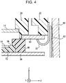
Fig. 4] Fig. 4 is an enlarged view of a region enclosed with a broken line inFig. 3 . - [
Fig. 5] Fig. 5 is a sectional view taken along line B-B inFig. 1 . - There has been a demand that imaging devices be shielded from dust and light and be capable of dissipating heat. An imaging apparatus and a mobile object according to an embodiment of the present disclosure can provide shielding to prevent entry of dust and light and enable dissipation of heat.
- Referring to
Figs. 1 to 5 , an imaging apparatus 1 according to an embodiment includes an imagingoptical system 10, aholding member 20, animaging substrate 30, anelastic member 40, a plate-like member 50, and ahousing 60. The imagingoptical system 10, theholding member 20, theimaging substrate 30, theelastic member 40, and the plate-like member 50 are accommodated in thehousing 60. Thehousing 60 may be made of a material such as resin. Thehousing 60 may be made of resin or may be made of various materials. - As illustrated in
Figs. 1 ,3 , and5 , the imagingoptical system 10 includes alens 12. Dash-dot lines inFigs. 3 and5 each denote anoptical axis 16 of thelens 12. As illustrated inFigs. 3 and5 , the imagingoptical system 10 may also include anoptical filter 14. Thelens 12 and theoptical filter 14 are also referred to as optical members. The imagingoptical system 10 includes at least one optical member. Thelens 12 of the imagingoptical system 10 forms an object image incident on the imaging apparatus 1. - The
holding member 20 holds thelens 12 and theoptical filter 14. Thelens 12 is joined to theholding member 20. Two ormore lenses 12, instead of thelens 12, may be included. At least one ofsuch lenses 12 may be replaced with another optical member, such as a mirror. Thelens 12 may be bonded to theholding member 20 with, for example, an adhesive. Thelens 12 may be joined to theholding member 20 via a fitting structure. Thelens 12 may be joined to theholding member 20 by fastening with screws or the like. - The
optical filter 14 may include, for example, an infrared (IR) cut filter. Theoptical filter 14 is joined to theholding member 20. When theoptical filter 14 is closest, among the optical members, to animaging device 32, theoptical filter 14 and theholding member 20 perform the function of sealing theimaging device 32. In this case, theoptical filter 14 is joined to theholding member 20 so as to prevent entry of foreign matter such as water and dust between theoptical filter 14 and theholding member 20. - Two or more
optical filters 14, instead of theoptical filter 14, may be included. Theoptical filters 14 may be bonded to theholding member 20 with, for example, an adhesive. Theholding member 20 may be made of a material such as resin. Theholding member 20 may be made of resin or may be made of various materials. - As illustrated in
Fig. 3 , theimaging device 32 is mounted on theimaging substrate 30. Theimaging device 32 includes a light-receivingregion 34 in anupper surface 38 of theimaging device 32. Theimaging device 32 is mounted on theimaging substrate 30 such that the light-receivingregion 34 faces the imagingoptical system 10. In addition to theimaging device 32, a circuit for processing data output from theimaging device 32 may be mounted on theimaging substrate 30. Theimaging substrate 30 may, for example, be a printed circuit board. - The
imaging substrate 30 is joined to the holdingmember 20. Theimaging substrate 30 may be bonded to the holdingmember 20 with, for example, an adhesive. Theimaging substrate 30 may be joined to the holdingmember 20 via a fitting structure. Theimaging substrate 30 may be joined to the holdingmember 20 by fastening with screws or the like. - The
imaging device 32 is disposed so that the light-receivingregion 34 is located in an image-forming plane of the imagingoptical system 10. An object image formed in the light-receivingregion 34 by the imagingoptical system 10 is captured by theimaging device 32. Theimaging device 32 may, for example, be a complementary metal oxide semiconductor (CMOS) image sensor or a charge-coupled device (CCD). - As illustrated in
Fig. 2 , theelastic member 40 surrounds the light-receivingregion 34 of theimaging device 32 without overlapping the light-receivingregion 34 when viewed in the direction of theoptical axis 16 of thelens 12. Theelastic member 40 is in contact with theupper surface 38 of theimaging device 32 and is shaped like a ring extending along the periphery of the light-receivingregion 34. The direction of theoptical axis 16 is also referred to as an optical axial direction. As illustrated inFigs. 3 ,4 , and5 , theelastic member 40 is located between the holdingmember 20 and theimaging device 32. Theelastic member 40 may be in contact with the holdingmember 20 such that the area of contact between them is ring-shaped. Theelastic member 40, together with the holdingmember 20 and theupper surface 38 of theimaging device 32, seals the light-receivingregion 34 of theimaging device 32. The light-receivingregion 34 of theimaging device 32 may thus be shielded from dust and light even further. - The
elastic member 40 may be in contact with an optical member that is closest, among optical members of the imagingoptical system 10, to theimaging device 32. In other words, theelastic member 40 may be in contact with at least one of the holdingmember 20 and the optical member that is closest, among the optical members, to theimaging device 32. For example, theelastic member 40 may be in contact with theoptical filter 14. In this case, theelastic member 40 and theoptical filter 14 seal the light-receivingregion 34 of theimaging device 32. - The
elastic member 40 may be made of, for example, silicone-based resin. The thermal conductivity of silicone-based resin is higher than polypropylene foam. When theelastic member 40 is made of a material of relatively high thermal conductivity, the diffusion of heat generated by theimaging device 32 into the holdingmember 20 through theelastic member 40 is promoted. The thermal dissipation properties of theimaging device 32 may be improved accordingly. - As illustrated in
Figs. 3 ,4 , and5 , theelastic member 40 may also be in contact with aside surface 36 of theimaging device 32. In this case, the diffusion of heat from theimaging device 32 and into theelastic member 40 is promoted even further as compared to the case where theelastic member 40 is not in contact with theside surface 36. The thermal dissipation properties of theimaging device 32 may be improved accordingly. - As illustrated in
Figs. 3 ,4 , and5 , the plate-like member 50 is located farther from theoptical axis 16 than the inside perimeter of theelastic member 40 and overlaps at least part of theelastic member 40 when viewed in the direction of theoptical axis 16 of thelens 12. The plate-like member 50 includes a portion in contact with the holdingmember 20 and a portion in contact with theelastic member 40. The contact between the plate-like member 50 and theelastic member 40 promotes the diffusion of heat generated by theimaging device 32 through theelastic member 40 and into the plate-like member 50. The contact between the plate-like member 50 and the holdingmember 20 further promotes the diffusion of heat into the holdingmember 20. - The plate-
like member 50 extends along the periphery of the light-receivingregion 34 of theimaging device 32. The plate-like member 50 may be shaped like a ring extending along the periphery of the light-receivingregion 34. The plate-like member 50 may be composed of two or more pieces disposed along the periphery of the light-receivingregion 34. The plate-like member 50 may be disposed in part of the region in which theelastic member 40 and the holdingmember 20 are in contact with each other along the periphery of the light-receivingregion 34. In this case, together with the holdingmember 20 and theelastic member 40, the plate-like member 50 disposed as above seals the light-receivingregion 34 of theimaging device 32. - The plate-
like member 50 may be made of a material whose thermal conductivity is higher than the thermal conductivity of theelastic member 40. The plate-like member 50 may be made of, for example, metal or may be made of a carbon-based material, such as a graphite sheet. Examples of the material of the plate-like member 50 are not limited to the above. The plate-like member 50 may be made of various materials that are more thermally conductive than theelastic member 40. - As illustrated in
Figs. 3 ,4 , and5 , thehousing 60 may include a shieldingportion 62. The shieldingportion 62 is made of a conductive material such as metal. The shieldingportion 62 is disposed so as to surround theimaging device 32 and is electrically connected to the ground point of the imaging apparatus 1 to provide electrostatic shielding for theimaging device 32. - As illustrated in
Fig. 5 , the plate-like member 50 may be disposed so as to cover at least part of theside surface 36 of theimaging device 32. The plate-like member 50 disposed as above can provide electrostatic shielding for theimaging device 32. - As illustrated in
Figs. 3 and4 , the plate-like member 50 includes abent portion 52. Thebent portion 52 may be obtained by partially bending the plate-like member 50. Thebent portion 52 is in contact with thehousing 60. Thebent portion 52 may be in contact with thehousing 60 with the shieldingportion 62 therebetween or may be in contact with thehousing 60 without the shieldingportion 62 therebetween. Thebent portion 52 in contact with thehousing 60 promotes diffusion of heat from theimaging device 32 to the plate-like member 50 further into thehousing 60. The thermal dissipation properties of theimaging device 32 may be improved accordingly. - The imaging apparatus 1 according to the present disclosure may be installed in a mobile object. The mobile object referred to in the present disclosure may be a vehicle, a ship, or an aircraft. Examples of the vehicle referred to in the present disclosure include automobiles and industrial vehicles and may also include rail cars, vehicles for non-industrial use, and fixed-wing aircrafts that run along runways. The vehicles include passenger cars, trucks, buses, two-wheelers, trolley buses, and other vehicles that travel on roads. The industrial vehicles include agricultural vehicles and construction vehicles. The industrial vehicles include forklifts and golf carts but are not limited to these examples. The industrial vehicles for agricultural use include tractors, cultivators, transplanters, binders, combines, and lawn mowers but are not limited to these examples. The industrial vehicles for construction work include bulldozers, scrapers, excavators, crane trucks, dump trucks, and road rollers but are not limited to these examples. The vehicles also include man-powered vehicles. The classification of vehicles is not limited to the above. For example, automobiles may include industrial vehicles that can travel on roads; that is, the same vehicle may be put into different classifications. Examples of the ship referred to in the present disclosure include marine jets, boats, and tankers. Examples of the aircraft referred to in the present disclosure include fixed-wing aircrafts and rotary wing aircrafts.
- The accompanying drawings are schematic representations of an embodiment of the present disclosure. Constituent elements are not drawn to scale, and the dimension ratios thereof are not necessarily fully corresponding to the actual dimension ratios.
- Although an embodiment of the present disclosure has been described above with reference to the accompanying drawings and by way of examples, various alterations or modifications may be made by those skilled in the art. It is to be understood that such alterations and modifications fall within the scope of the present disclosure. For example, functions and the like of each constituent part or each step can be rearranged in any way that involves no logical inconsistency, and constituent parts or steps can be combined into one or divided. While the present disclosure has been described above with a focus on an embodiment in the form of an apparatus, the present disclosure may be embodied in the form of a method that includes steps performed by constituent parts of an apparatus. Furthermore, the present disclosure may be embodied in the form of a method or program executed by a processor included in an apparatus or may be embodied in the form of a recording medium on which a program is recorded. It is to be understood that such embodiments also fall within the scope of the present disclosure.
- The words "first", "second", and so on in the present disclosure are identifiers for distinguishing between constituent elements. With the constituent elements being distinguishable by "first", "second", and so on in the present disclosure, the identifiers assigned to these constituent elements are interchangeable. For example, the identifiers "first" and "second" that are assigned to the respective lenses are interchangeable. The identifiers are to be interchanged all at once. The elements remain distinguishable from each other after interchanges of identifiers. The identifiers may be omitted. Constituent elements from which the identifiers are omitted are distinguished by reference signs. In the present disclosure, the identifiers "first", "second" and so on should not be used for interpretation of the order of the constituent elements or should not be used as grounds for the presence of lower numbered identifiers.
- In the present disclosure, the X-axis, the Y-axis, and the Z-axis are provided for convenience of illustration and are interchangeable. Constituent elements referred to in the present disclosure have been described using the Cartesian coordinate system based on coordinate axes: the X-axis, the Y-axis, and the Z-axis. It is not required that the constituent elements referred to the present disclosure be orthogonal to each other.
-
- 1 imaging apparatus
- 10 imaging optical system (12: lens, 14: filter)
- 20 holding member
- 30 imaging substrate
- 32 imaging device (34: light-receiving region, 36: side surface, 38: upper surface)
- 40 elastic member
- 50 plate-like member (52: bent portion)
- 60 housing (62: shielding portion)
Claims (10)
- An imaging apparatus, comprising:an imaging optical system including at least one optical member;a holding member that holds the imaging optical system;an imaging device that includes a light-receiving region and is located in an image-forming plane of the imaging optical system;an elastic member that is located close to the imaging device toward the imaging optical system and surrounds the light-receiving region without overlapping the light-receiving region when viewed in an optical axial direction of the imaging optical system, the elastic member being in contact with the imaging device such that an area of contact between the elastic member and the imaging device is ring-shaped; anda plate-like member that is located farther from an optical axis of the imaging optical system than an inside perimeter of the elastic member and overlaps at least part of the elastic member when viewed in the optical axial direction of the imaging optical system, the plate-like member including a portion in contact with the holding member and a portion in contact with the elastic member.
- The imaging apparatus according to Claim 1, wherein the elastic member is in contact with at least one of the holding member and the optical member that is closest, in the at least one optical member, to the imaging device.
- The imaging apparatus according to Claim 1, wherein the elastic member is in contact with at least part of a side surface of the imaging device.
- The imaging apparatus according to Claim 2, wherein the elastic member is in contact with at least part of a side surface of the imaging device.
- The imaging apparatus according to Claim 1, wherein the plate-like member covers at least part of a side surface of the imaging device.
- The imaging apparatus according to Claim 2, wherein the plate-like member covers at least part of a side surface of the imaging device.
- The imaging apparatus according to Claim 3, wherein the plate-like member covers at least part of the side surface of the imaging device.
- The imaging apparatus according to Claim 4, wherein the plate-like member covers at least part of the side surface of the imaging device.
- The imaging apparatus according to any one of Claims 1 to 8, further comprisinga housing in which the imaging optical system, the holding member, the imaging device, the elastic member, and the plate-like member are accommodated, whereinat least part of the plate-like member is in contact with the housing.
- A mobile object in which an imaging apparatus is installed,
the imaging apparatus comprisingan imaging optical system including at least one optical member,a holding member that holds the imaging optical system,an imaging device that includes a light-receiving region and is located in an image-forming plane of the imaging optical system,an elastic member that is located close to the imaging device toward the imaging optical system and surrounds the light-receiving region without overlapping the light-receiving region when viewed in an optical axial direction of the imaging optical system, the elastic member being in contact with the imaging device such that an area of contact between the elastic member and the imaging device is ring-shaped, anda plate-like member that is located farther from an optical axis of the imaging optical system than an inside perimeter of the elastic member and overlaps at least part of the elastic member when viewed in the optical axial direction of the imaging optical system, the plate-like member including a portion in contact with the holding member and a portion in contact with the elastic member.
Applications Claiming Priority (2)
| Application Number | Priority Date | Filing Date | Title |
|---|---|---|---|
| JP2019176130A JP7263193B2 (en) | 2019-09-26 | 2019-09-26 | Imaging device and moving object |
| PCT/JP2020/033939 WO2021059965A1 (en) | 2019-09-26 | 2020-09-08 | Imaging device and mobile body |
Publications (3)
| Publication Number | Publication Date |
|---|---|
| EP4037301A1 true EP4037301A1 (en) | 2022-08-03 |
| EP4037301A4 EP4037301A4 (en) | 2023-08-23 |
| EP4037301B1 EP4037301B1 (en) | 2024-11-06 |
Family
ID=75165706
Family Applications (1)
| Application Number | Title | Priority Date | Filing Date |
|---|---|---|---|
| EP20870107.8A Active EP4037301B1 (en) | 2019-09-26 | 2020-09-08 | Imaging device and mobile body |
Country Status (5)
| Country | Link |
|---|---|
| US (1) | US11754911B2 (en) |
| EP (1) | EP4037301B1 (en) |
| JP (1) | JP7263193B2 (en) |
| CN (1) | CN114450931B (en) |
| WO (1) | WO2021059965A1 (en) |
Families Citing this family (4)
| Publication number | Priority date | Publication date | Assignee | Title |
|---|---|---|---|---|
| WO2023032295A1 (en) * | 2021-09-01 | 2023-03-09 | ソニーセミコンダクタソリューションズ株式会社 | Sensor module and method for manufacturing sensor module |
| JP7770254B2 (en) * | 2022-06-01 | 2025-11-14 | 京セラ株式会社 | Imaging device |
| JP2025069807A (en) * | 2023-10-18 | 2025-05-01 | パナソニックIpマネジメント株式会社 | Imaging device |
| JP2025101274A (en) * | 2023-12-25 | 2025-07-07 | キヤノン株式会社 | Imaging device |
Family Cites Families (13)
| Publication number | Priority date | Publication date | Assignee | Title |
|---|---|---|---|---|
| JP2006295714A (en) | 2005-04-13 | 2006-10-26 | Olympus Corp | Imaging device |
| WO2010029731A1 (en) * | 2008-09-11 | 2010-03-18 | パナソニック株式会社 | Imaging device |
| JP5126257B2 (en) * | 2010-03-12 | 2013-01-23 | オムロン株式会社 | Imaging device |
| JP5850810B2 (en) | 2012-07-25 | 2016-02-03 | 日立オートモティブシステムズ株式会社 | Imaging device and method for manufacturing the same |
| KR102213657B1 (en) | 2014-01-28 | 2021-02-08 | 엘지이노텍 주식회사 | Camera module |
| JP6638151B2 (en) * | 2014-07-04 | 2020-01-29 | 日本電産コパル株式会社 | Imaging device |
| US9769361B2 (en) * | 2015-08-31 | 2017-09-19 | Adlink Technology Inc. | Assembly structure for industrial cameras |
| EP3472570A4 (en) * | 2016-06-16 | 2020-02-12 | Novadaq Technologies ULC | ADJUSTABLE SENSOR MOUNTING SYSTEMS WITH CLOSED CAVITY AND METHOD |
| JP6827341B2 (en) | 2017-02-23 | 2021-02-10 | リズム株式会社 | Information processing equipment, cameras and camera equipment |
| FR3067131B1 (en) | 2017-06-01 | 2019-06-21 | Aptiv Technologies Limited | OPTICAL DEVICE FOR VEHICLE COMPRISING A HEATING ELEMENT |
| US10911727B2 (en) | 2017-06-16 | 2021-02-02 | Apple Inc. | Image sensor with optical communication capabilities |
| JP6957235B2 (en) * | 2017-06-28 | 2021-11-02 | 京セラ株式会社 | Imaging device and moving object |
| JP6912398B2 (en) | 2018-01-29 | 2021-08-04 | 京セラ株式会社 | Fixed structure, imaging device and mobile |
-
2019
- 2019-09-26 JP JP2019176130A patent/JP7263193B2/en active Active
-
2020
- 2020-09-08 EP EP20870107.8A patent/EP4037301B1/en active Active
- 2020-09-08 CN CN202080067701.0A patent/CN114450931B/en active Active
- 2020-09-08 US US17/754,048 patent/US11754911B2/en active Active
- 2020-09-08 WO PCT/JP2020/033939 patent/WO2021059965A1/en not_active Ceased
Also Published As
| Publication number | Publication date |
|---|---|
| EP4037301B1 (en) | 2024-11-06 |
| US20220334455A1 (en) | 2022-10-20 |
| JP2021057628A (en) | 2021-04-08 |
| US11754911B2 (en) | 2023-09-12 |
| CN114450931A (en) | 2022-05-06 |
| JP7263193B2 (en) | 2023-04-24 |
| CN114450931B (en) | 2024-08-23 |
| EP4037301A4 (en) | 2023-08-23 |
| WO2021059965A1 (en) | 2021-04-01 |
Similar Documents
| Publication | Publication Date | Title |
|---|---|---|
| US11754911B2 (en) | Imaging apparatus and mobile object | |
| JP7074706B2 (en) | Electronic devices, imaging devices, and moving objects | |
| EP3961300B1 (en) | Electronic instrument, imaging device, and mobile body | |
| US12028591B2 (en) | Imaging apparatus and mobile object | |
| JP2022000716A (en) | Imaging device and moving body | |
| EP3944606B1 (en) | Electronic instrument, image capture device, and mobile body | |
| US11543614B2 (en) | Imaging apparatus, mobile object, and manufacturing method | |
| JP6905958B2 (en) | Adhesive structures, imaging devices, and moving objects | |
| US20260036807A1 (en) | Vehicular camera | |
| JP7466017B2 (en) | Imaging device and moving object | |
| CN113614618B (en) | Image display module, moving body, and concave mirror | |
| CN121509794A (en) | Imaging device | |
| WO2021235255A1 (en) | Image display module |
Legal Events
| Date | Code | Title | Description |
|---|---|---|---|
| STAA | Information on the status of an ep patent application or granted ep patent |
Free format text: STATUS: THE INTERNATIONAL PUBLICATION HAS BEEN MADE |
|
| PUAI | Public reference made under article 153(3) epc to a published international application that has entered the european phase |
Free format text: ORIGINAL CODE: 0009012 |
|
| STAA | Information on the status of an ep patent application or granted ep patent |
Free format text: STATUS: REQUEST FOR EXAMINATION WAS MADE |
|
| 17P | Request for examination filed |
Effective date: 20220322 |
|
| AK | Designated contracting states |
Kind code of ref document: A1 Designated state(s): AL AT BE BG CH CY CZ DE DK EE ES FI FR GB GR HR HU IE IS IT LI LT LU LV MC MK MT NL NO PL PT RO RS SE SI SK SM TR |
|
| DAV | Request for validation of the european patent (deleted) | ||
| DAX | Request for extension of the european patent (deleted) | ||
| P01 | Opt-out of the competence of the unified patent court (upc) registered |
Effective date: 20230505 |
|
| REG | Reference to a national code |
Ref country code: DE Free format text: PREVIOUS MAIN CLASS: H04N0005225000 Ipc: G02B0007020000 Ref country code: DE Ref legal event code: R079 Ref document number: 602020041042 Country of ref document: DE Free format text: PREVIOUS MAIN CLASS: H04N0005225000 Ipc: G02B0007020000 |
|
| A4 | Supplementary search report drawn up and despatched |
Effective date: 20230726 |
|
| RIC1 | Information provided on ipc code assigned before grant |
Ipc: H04N 23/55 20230101ALI20230720BHEP Ipc: H04N 23/54 20230101ALI20230720BHEP Ipc: H04N 23/51 20230101ALI20230720BHEP Ipc: G03B 11/04 20210101ALI20230720BHEP Ipc: H04N 23/50 20230101ALI20230720BHEP Ipc: H04N 23/52 20230101ALI20230720BHEP Ipc: G03B 37/00 20210101ALI20230720BHEP Ipc: G03B 17/55 20210101ALI20230720BHEP Ipc: G03B 17/02 20210101ALI20230720BHEP Ipc: G03B 15/00 20210101ALI20230720BHEP Ipc: G02B 7/02 20210101AFI20230720BHEP |
|
| GRAP | Despatch of communication of intention to grant a patent |
Free format text: ORIGINAL CODE: EPIDOSNIGR1 |
|
| STAA | Information on the status of an ep patent application or granted ep patent |
Free format text: STATUS: GRANT OF PATENT IS INTENDED |
|
| INTG | Intention to grant announced |
Effective date: 20240528 |
|
| GRAS | Grant fee paid |
Free format text: ORIGINAL CODE: EPIDOSNIGR3 |
|
| GRAA | (expected) grant |
Free format text: ORIGINAL CODE: 0009210 |
|
| STAA | Information on the status of an ep patent application or granted ep patent |
Free format text: STATUS: THE PATENT HAS BEEN GRANTED |
|
| AK | Designated contracting states |
Kind code of ref document: B1 Designated state(s): AL AT BE BG CH CY CZ DE DK EE ES FI FR GB GR HR HU IE IS IT LI LT LU LV MC MK MT NL NO PL PT RO RS SE SI SK SM TR |
|
| REG | Reference to a national code |
Ref country code: GB Ref legal event code: FG4D |
|
| REG | Reference to a national code |
Ref country code: CH Ref legal event code: EP |
|
| REG | Reference to a national code |
Ref country code: DE Ref legal event code: R096 Ref document number: 602020041042 Country of ref document: DE |
|
| REG | Reference to a national code |
Ref country code: IE Ref legal event code: FG4D |
|
| REG | Reference to a national code |
Ref country code: LT Ref legal event code: MG9D |
|
| REG | Reference to a national code |
Ref country code: NL Ref legal event code: MP Effective date: 20241106 |
|
| PG25 | Lapsed in a contracting state [announced via postgrant information from national office to epo] |
Ref country code: PT Free format text: LAPSE BECAUSE OF FAILURE TO SUBMIT A TRANSLATION OF THE DESCRIPTION OR TO PAY THE FEE WITHIN THE PRESCRIBED TIME-LIMIT Effective date: 20250306 Ref country code: IS Free format text: LAPSE BECAUSE OF FAILURE TO SUBMIT A TRANSLATION OF THE DESCRIPTION OR TO PAY THE FEE WITHIN THE PRESCRIBED TIME-LIMIT Effective date: 20250306 Ref country code: HR Free format text: LAPSE BECAUSE OF FAILURE TO SUBMIT A TRANSLATION OF THE DESCRIPTION OR TO PAY THE FEE WITHIN THE PRESCRIBED TIME-LIMIT Effective date: 20241106 |
|
| PG25 | Lapsed in a contracting state [announced via postgrant information from national office to epo] |
Ref country code: FI Free format text: LAPSE BECAUSE OF FAILURE TO SUBMIT A TRANSLATION OF THE DESCRIPTION OR TO PAY THE FEE WITHIN THE PRESCRIBED TIME-LIMIT Effective date: 20241106 Ref country code: NL Free format text: LAPSE BECAUSE OF FAILURE TO SUBMIT A TRANSLATION OF THE DESCRIPTION OR TO PAY THE FEE WITHIN THE PRESCRIBED TIME-LIMIT Effective date: 20241106 |
|
| REG | Reference to a national code |
Ref country code: AT Ref legal event code: MK05 Ref document number: 1739975 Country of ref document: AT Kind code of ref document: T Effective date: 20241106 |
|
| PG25 | Lapsed in a contracting state [announced via postgrant information from national office to epo] |
Ref country code: BG Free format text: LAPSE BECAUSE OF FAILURE TO SUBMIT A TRANSLATION OF THE DESCRIPTION OR TO PAY THE FEE WITHIN THE PRESCRIBED TIME-LIMIT Effective date: 20241106 |
|
| PG25 | Lapsed in a contracting state [announced via postgrant information from national office to epo] |
Ref country code: ES Free format text: LAPSE BECAUSE OF FAILURE TO SUBMIT A TRANSLATION OF THE DESCRIPTION OR TO PAY THE FEE WITHIN THE PRESCRIBED TIME-LIMIT Effective date: 20241106 |
|
| PG25 | Lapsed in a contracting state [announced via postgrant information from national office to epo] |
Ref country code: NO Free format text: LAPSE BECAUSE OF FAILURE TO SUBMIT A TRANSLATION OF THE DESCRIPTION OR TO PAY THE FEE WITHIN THE PRESCRIBED TIME-LIMIT Effective date: 20250206 |
|
| PG25 | Lapsed in a contracting state [announced via postgrant information from national office to epo] |
Ref country code: GR Free format text: LAPSE BECAUSE OF FAILURE TO SUBMIT A TRANSLATION OF THE DESCRIPTION OR TO PAY THE FEE WITHIN THE PRESCRIBED TIME-LIMIT Effective date: 20250207 Ref country code: LV Free format text: LAPSE BECAUSE OF FAILURE TO SUBMIT A TRANSLATION OF THE DESCRIPTION OR TO PAY THE FEE WITHIN THE PRESCRIBED TIME-LIMIT Effective date: 20241106 Ref country code: AT Free format text: LAPSE BECAUSE OF FAILURE TO SUBMIT A TRANSLATION OF THE DESCRIPTION OR TO PAY THE FEE WITHIN THE PRESCRIBED TIME-LIMIT Effective date: 20241106 |
|
| PG25 | Lapsed in a contracting state [announced via postgrant information from national office to epo] |
Ref country code: PL Free format text: LAPSE BECAUSE OF FAILURE TO SUBMIT A TRANSLATION OF THE DESCRIPTION OR TO PAY THE FEE WITHIN THE PRESCRIBED TIME-LIMIT Effective date: 20241106 |
|
| PG25 | Lapsed in a contracting state [announced via postgrant information from national office to epo] |
Ref country code: RS Free format text: LAPSE BECAUSE OF FAILURE TO SUBMIT A TRANSLATION OF THE DESCRIPTION OR TO PAY THE FEE WITHIN THE PRESCRIBED TIME-LIMIT Effective date: 20250206 |
|
| PG25 | Lapsed in a contracting state [announced via postgrant information from national office to epo] |
Ref country code: SM Free format text: LAPSE BECAUSE OF FAILURE TO SUBMIT A TRANSLATION OF THE DESCRIPTION OR TO PAY THE FEE WITHIN THE PRESCRIBED TIME-LIMIT Effective date: 20241106 |
|
| PG25 | Lapsed in a contracting state [announced via postgrant information from national office to epo] |
Ref country code: DK Free format text: LAPSE BECAUSE OF FAILURE TO SUBMIT A TRANSLATION OF THE DESCRIPTION OR TO PAY THE FEE WITHIN THE PRESCRIBED TIME-LIMIT Effective date: 20241106 |
|
| PG25 | Lapsed in a contracting state [announced via postgrant information from national office to epo] |
Ref country code: EE Free format text: LAPSE BECAUSE OF FAILURE TO SUBMIT A TRANSLATION OF THE DESCRIPTION OR TO PAY THE FEE WITHIN THE PRESCRIBED TIME-LIMIT Effective date: 20241106 |
|
| PG25 | Lapsed in a contracting state [announced via postgrant information from national office to epo] |
Ref country code: RO Free format text: LAPSE BECAUSE OF FAILURE TO SUBMIT A TRANSLATION OF THE DESCRIPTION OR TO PAY THE FEE WITHIN THE PRESCRIBED TIME-LIMIT Effective date: 20241106 |
|
| PG25 | Lapsed in a contracting state [announced via postgrant information from national office to epo] |
Ref country code: SK Free format text: LAPSE BECAUSE OF FAILURE TO SUBMIT A TRANSLATION OF THE DESCRIPTION OR TO PAY THE FEE WITHIN THE PRESCRIBED TIME-LIMIT Effective date: 20241106 |
|
| PG25 | Lapsed in a contracting state [announced via postgrant information from national office to epo] |
Ref country code: CZ Free format text: LAPSE BECAUSE OF FAILURE TO SUBMIT A TRANSLATION OF THE DESCRIPTION OR TO PAY THE FEE WITHIN THE PRESCRIBED TIME-LIMIT Effective date: 20241106 |
|
| PG25 | Lapsed in a contracting state [announced via postgrant information from national office to epo] |
Ref country code: IT Free format text: LAPSE BECAUSE OF FAILURE TO SUBMIT A TRANSLATION OF THE DESCRIPTION OR TO PAY THE FEE WITHIN THE PRESCRIBED TIME-LIMIT Effective date: 20241106 |
|
| REG | Reference to a national code |
Ref country code: DE Ref legal event code: R097 Ref document number: 602020041042 Country of ref document: DE |
|
| PG25 | Lapsed in a contracting state [announced via postgrant information from national office to epo] |
Ref country code: SE Free format text: LAPSE BECAUSE OF FAILURE TO SUBMIT A TRANSLATION OF THE DESCRIPTION OR TO PAY THE FEE WITHIN THE PRESCRIBED TIME-LIMIT Effective date: 20241106 |
|
| PLBE | No opposition filed within time limit |
Free format text: ORIGINAL CODE: 0009261 |
|
| STAA | Information on the status of an ep patent application or granted ep patent |
Free format text: STATUS: NO OPPOSITION FILED WITHIN TIME LIMIT |
|
| PGFP | Annual fee paid to national office [announced via postgrant information from national office to epo] |
Ref country code: DE Payment date: 20250730 Year of fee payment: 6 |
|
| 26N | No opposition filed |
Effective date: 20250807 |
|
| PGFP | Annual fee paid to national office [announced via postgrant information from national office to epo] |
Ref country code: GB Payment date: 20250731 Year of fee payment: 6 |
|
| PGFP | Annual fee paid to national office [announced via postgrant information from national office to epo] |
Ref country code: FR Payment date: 20250808 Year of fee payment: 6 |