EP4037169A1 - Control circuit for a power suuply and power supply with reduced standby power losses - Google Patents
Control circuit for a power suuply and power supply with reduced standby power losses Download PDFInfo
- Publication number
- EP4037169A1 EP4037169A1 EP21154050.5A EP21154050A EP4037169A1 EP 4037169 A1 EP4037169 A1 EP 4037169A1 EP 21154050 A EP21154050 A EP 21154050A EP 4037169 A1 EP4037169 A1 EP 4037169A1
- Authority
- EP
- European Patent Office
- Prior art keywords
- output
- power supply
- output capacitor
- control circuit
- mode
- Prior art date
- Legal status (The legal status is an assumption and is not a legal conclusion. Google has not performed a legal analysis and makes no representation as to the accuracy of the status listed.)
- Pending
Links
Images



Classifications
-
- H—ELECTRICITY
- H02—GENERATION; CONVERSION OR DISTRIBUTION OF ELECTRIC POWER
- H02M—APPARATUS FOR CONVERSION BETWEEN AC AND AC, BETWEEN AC AND DC, OR BETWEEN DC AND DC, AND FOR USE WITH MAINS OR SIMILAR POWER SUPPLY SYSTEMS; CONVERSION OF DC OR AC INPUT POWER INTO SURGE OUTPUT POWER; CONTROL OR REGULATION THEREOF
- H02M1/00—Details of apparatus for conversion
- H02M1/0003—Details of control, feedback or regulation circuits
- H02M1/0032—Control circuits allowing low power mode operation, e.g. in standby mode
- H02M1/0035—Control circuits allowing low power mode operation, e.g. in standby mode using burst mode control
-
- H—ELECTRICITY
- H02—GENERATION; CONVERSION OR DISTRIBUTION OF ELECTRIC POWER
- H02J—ELECTRIC POWER NETWORKS; CIRCUIT ARRANGEMENTS OR SYSTEMS FOR SUPPLYING OR DISTRIBUTING ELECTRIC POWER; SYSTEMS FOR STORING ELECTRIC ENERGY
- H02J7/00—Circuit arrangements for charging or discharging batteries or for supplying loads from batteries
- H02J7/34—Parallel operation in networks using both storage and other DC sources, e.g. providing buffering
- H02J7/345—Parallel operation in networks using both storage and other DC sources, e.g. providing buffering using capacitors as storage or buffering devices
-
- H—ELECTRICITY
- H02—GENERATION; CONVERSION OR DISTRIBUTION OF ELECTRIC POWER
- H02J—ELECTRIC POWER NETWORKS; CIRCUIT ARRANGEMENTS OR SYSTEMS FOR SUPPLYING OR DISTRIBUTING ELECTRIC POWER; SYSTEMS FOR STORING ELECTRIC ENERGY
- H02J7/00—Circuit arrangements for charging or discharging batteries or for supplying loads from batteries
- H02J7/865—Battery or charger load switching, e.g. concurrent charging and load supply
-
- H—ELECTRICITY
- H02—GENERATION; CONVERSION OR DISTRIBUTION OF ELECTRIC POWER
- H02J—ELECTRIC POWER NETWORKS; CIRCUIT ARRANGEMENTS OR SYSTEMS FOR SUPPLYING OR DISTRIBUTING ELECTRIC POWER; SYSTEMS FOR STORING ELECTRIC ENERGY
- H02J9/00—Circuit arrangements for emergency or stand-by power supply, e.g. for emergency lighting
- H02J9/04—Circuit arrangements for emergency or stand-by power supply, e.g. for emergency lighting in which the distribution system is disconnected from the normal source and connected to a standby source
- H02J9/06—Circuit arrangements for emergency or stand-by power supply, e.g. for emergency lighting in which the distribution system is disconnected from the normal source and connected to a standby source with automatic change-over, e.g. UPS systems
- H02J9/061—Circuit arrangements for emergency or stand-by power supply, e.g. for emergency lighting in which the distribution system is disconnected from the normal source and connected to a standby source with automatic change-over, e.g. UPS systems for DC powered loads
-
- H—ELECTRICITY
- H02—GENERATION; CONVERSION OR DISTRIBUTION OF ELECTRIC POWER
- H02M—APPARATUS FOR CONVERSION BETWEEN AC AND AC, BETWEEN AC AND DC, OR BETWEEN DC AND DC, AND FOR USE WITH MAINS OR SIMILAR POWER SUPPLY SYSTEMS; CONVERSION OF DC OR AC INPUT POWER INTO SURGE OUTPUT POWER; CONTROL OR REGULATION THEREOF
- H02M1/00—Details of apparatus for conversion
-
- H—ELECTRICITY
- H02—GENERATION; CONVERSION OR DISTRIBUTION OF ELECTRIC POWER
- H02M—APPARATUS FOR CONVERSION BETWEEN AC AND AC, BETWEEN AC AND DC, OR BETWEEN DC AND DC, AND FOR USE WITH MAINS OR SIMILAR POWER SUPPLY SYSTEMS; CONVERSION OF DC OR AC INPUT POWER INTO SURGE OUTPUT POWER; CONTROL OR REGULATION THEREOF
- H02M1/00—Details of apparatus for conversion
- H02M1/14—Arrangements for reducing ripples from DC input or output
- H02M1/15—Arrangements for reducing ripples from DC input or output using active elements
-
- H—ELECTRICITY
- H02—GENERATION; CONVERSION OR DISTRIBUTION OF ELECTRIC POWER
- H02M—APPARATUS FOR CONVERSION BETWEEN AC AND AC, BETWEEN AC AND DC, OR BETWEEN DC AND DC, AND FOR USE WITH MAINS OR SIMILAR POWER SUPPLY SYSTEMS; CONVERSION OF DC OR AC INPUT POWER INTO SURGE OUTPUT POWER; CONTROL OR REGULATION THEREOF
- H02M3/00—Conversion of DC power input into DC power output
- H02M3/02—Conversion of DC power input into DC power output without intermediate conversion into AC
- H02M3/04—Conversion of DC power input into DC power output without intermediate conversion into AC by static converters
- H02M3/06—Conversion of DC power input into DC power output without intermediate conversion into AC by static converters using resistors or capacitors, e.g. potential divider
- H02M3/07—Conversion of DC power input into DC power output without intermediate conversion into AC by static converters using resistors or capacitors, e.g. potential divider using capacitors charged and discharged alternately by semiconductor devices with control electrode, e.g. charge pumps
-
- H—ELECTRICITY
- H02—GENERATION; CONVERSION OR DISTRIBUTION OF ELECTRIC POWER
- H02M—APPARATUS FOR CONVERSION BETWEEN AC AND AC, BETWEEN AC AND DC, OR BETWEEN DC AND DC, AND FOR USE WITH MAINS OR SIMILAR POWER SUPPLY SYSTEMS; CONVERSION OF DC OR AC INPUT POWER INTO SURGE OUTPUT POWER; CONTROL OR REGULATION THEREOF
- H02M1/00—Details of apparatus for conversion
- H02M1/0003—Details of control, feedback or regulation circuits
- H02M1/0025—Arrangements for modifying reference values, feedback values or error values in the control loop of a converter
-
- H—ELECTRICITY
- H02—GENERATION; CONVERSION OR DISTRIBUTION OF ELECTRIC POWER
- H02M—APPARATUS FOR CONVERSION BETWEEN AC AND AC, BETWEEN AC AND DC, OR BETWEEN DC AND DC, AND FOR USE WITH MAINS OR SIMILAR POWER SUPPLY SYSTEMS; CONVERSION OF DC OR AC INPUT POWER INTO SURGE OUTPUT POWER; CONTROL OR REGULATION THEREOF
- H02M3/00—Conversion of DC power input into DC power output
- H02M3/22—Conversion of DC power input into DC power output with intermediate conversion into AC
- H02M3/24—Conversion of DC power input into DC power output with intermediate conversion into AC by static converters
- H02M3/28—Conversion of DC power input into DC power output with intermediate conversion into AC by static converters using discharge tubes with control electrode or semiconductor devices with control electrode to produce the intermediate AC
- H02M3/325—Conversion of DC power input into DC power output with intermediate conversion into AC by static converters using discharge tubes with control electrode or semiconductor devices with control electrode to produce the intermediate AC using devices of a triode or a transistor type requiring continuous application of a control signal
- H02M3/335—Conversion of DC power input into DC power output with intermediate conversion into AC by static converters using discharge tubes with control electrode or semiconductor devices with control electrode to produce the intermediate AC using devices of a triode or a transistor type requiring continuous application of a control signal using semiconductor devices only
- H02M3/33507—Conversion of DC power input into DC power output with intermediate conversion into AC by static converters using discharge tubes with control electrode or semiconductor devices with control electrode to produce the intermediate AC using devices of a triode or a transistor type requiring continuous application of a control signal using semiconductor devices only with automatic control of the output voltage or current, e.g. flyback converters
-
- Y—GENERAL TAGGING OF NEW TECHNOLOGICAL DEVELOPMENTS; GENERAL TAGGING OF CROSS-SECTIONAL TECHNOLOGIES SPANNING OVER SEVERAL SECTIONS OF THE IPC; TECHNICAL SUBJECTS COVERED BY FORMER USPC CROSS-REFERENCE ART COLLECTIONS [XRACs] AND DIGESTS
- Y02—TECHNOLOGIES OR APPLICATIONS FOR MITIGATION OR ADAPTATION AGAINST CLIMATE CHANGE
- Y02B—CLIMATE CHANGE MITIGATION TECHNOLOGIES RELATED TO BUILDINGS, e.g. HOUSING, HOUSE APPLIANCES OR RELATED END-USER APPLICATIONS
- Y02B70/00—Technologies for an efficient end-user side electric power management and consumption
- Y02B70/10—Technologies improving the efficiency by using switched-mode power supplies [SMPS], i.e. efficient power electronics conversion e.g. power factor correction or reduction of losses in power supplies or efficient standby modes
Definitions
- This disclosure relates in general to a power supply, in particular, a switched-mode power supply.
- a switched mode power supply includes an input configured to receive an input power and an output configured to have a load connected thereto.
- the SMPS may operate in a normal operating mode when a load is connected to the output and provide a regulated output voltage to the load in the normal operating mode.
- the SMPS Before a load is connected to the SMPS or after the load has been disconnected, the SMPS may operate in a standby mode. In the standby mode, the input power is lower than in a normal operating mode, but is not zero. In the standby mode, the input power is mainly used to supply control circuitry of the SMPS. Supplying the control circuitry in the standby mode enables the SMPS to detect when a load is connected and to enter the normal operating as soon as the load has been connected.
- the control circuit is configured to activate a second output capacitor connected in parallel with a first output capacitor of a power supply when the power supply is in a normal operating mode, and deactivate the second output capacitor when the power supply is in a standby mode.
- the power supply includes a converter stage having an input and an output, an output circuit connected to the output of the converter stage, and a control circuit.
- the output circuit includes a first output capacitor connected to the output of the converter stage, and a second output capacitor.
- the control circuit is configured to activate the second output capacitor when the power supply is in a normal operating mode, and deactivate the second output capacitor when the power supply is in a standby mode.
- the method includes operating a power supply in a normal operating mode or a standby mode, wherein operating the power supply in the standby mode includes activating a second output capacitor connected in parallel with a first output capacitor of the power supply, and wherein operating the power supply in the normal operating mode comprises deactivating the second output capacitor.
- Figure 1 shows a circuit diagram of a switched-mode power supply (SMPS) according to one example.
- the power supply includes a switched-mode converter stage 1 with an input 11, 12, configured to receive an input voltage Vin and an input current Iin and an output 13, 14, configured to provide an output voltage Vout and an output current lout based on the input voltage Vin and the input current Iin.
- the input voltage Vin is a direct voltage.
- the power supply further includes an output circuit 2.
- the output circuit includes a first output capacitor 21 and a second output capacitor 22.
- the first output capacitor 21 is coupled to the output 13, 14, more specifically, the output capacitor 21 is coupled between a first output node 13 and a second output node 14 of the output 13, 14 of the converter stage 1.
- the second output capacitor is configured to be activated or deactivated. That is, the second output capacitor 22 is configured to be connected in parallel with the first output capacitor 21 or to be disconnected from the first output capacitor 21.
- the output circuit 2 includes a first electronic switch 23.
- This first electronic switch 23 is connected in series with the second output capacitor 22, wherein the series circuit including the second output capacitor 22 and the first electronic switch 23 is connected in parallel with the first output capacitor 21.
- the circuit with the first output capacitor 21, the second output capacitor 22 and the first electronic switch 23 is also referred to as output capacitor circuit 20 in the following.
- the output circuit 2 further includes an output 25, 26 that is configured to provide a supply voltage Vbus to a load (illustrated in dashed lines in Figure 1 ).
- a second electronic switch 24 is connected between the output capacitor circuit 20 and the output 25, 26. This second electronic switch 24 can be switched on (activated) or switched off (deactivated). When the second electronic switch 24 is switched on, the output capacitor circuit 20 is connected to the output 25, 26, so that the supply voltage Vbus available at the output 25, 26 essentially equals the output voltage Vout provided by the converter stage 1 (a voltage drop across the second electronic switch 24 is negligible). When the second electronic switch 24 is switched off, the output capacitor circuit 20 is disconnected from the output 25, 26. In this case, the supply voltage Vbus is defined by the load and a power transfer from the converter stage 1 to the load is interrupted.
- the second electronic switch 24 is connected between the first output node 13 of the converter stage 1 and the a first output node 25 of the output circuit 2.
- the second electronic switch 24 is connected between the second output node 14 of the converter stage 1 and the second output node 26 of the output circuit 2. In each case, a power transfer between the converter stage 1 and the output 25, 26 of the output circuit 2 is interrupted when the second electronic switch 24 is switched off.
- any kind of conventional electronic switch may be used to implement the first and second electronic switch 23, 24.
- Examples of a conventional electronic switch include, but are not restricted to, a MOSFET (Metal Oxide Semiconductor Field-Effect Transistor), an IGBT (Insulated Gate Bipolar Transistors), a HEMT (High Electron Mobility Transistor), a JFET (Junction Field-Effect Transistor), or combinations thereof.
- the second electronic switch 24 is a bidirectional blocking electronic switch that includes two MOSFETs in a series configuration such that body diodes of the two MOSFETs are in a back-to-back configuration.
- the input 11, 12 of the converter stage 1 forms an input of the power supply and the output 25, 26 of the output circuit 2 forms an output of the power supply.
- the output circuit 2 further includes a third output capacitor 28 that is connected between the output nodes 25, 26.
- a capacitance of this capacitor may be much smaller than a capacitance of the first output capacitor 21.
- the capacitance of the third output capacitor 28 is less than 10%, less than 5%, or less than 2% of the capacitance of the first output capacitor 21.
- the capacitance of the first output capacitor is between 30 microfarads ( ⁇ F) and 100 microfarads, for example.
- the capacitance of the second output capacitor 21 is higher than the capacitance of the first output capacitor 21.
- the capacitance of the second output capacitor 22 is at least 2 times, at least 3 times, at least 5 times, or at least 10 times the capacitance of the first output capacitor 21.
- the power supply shown in Figure 1 may be part of a so-called USB (Universal Serial Bus) PD (Power Delivery) device.
- the USB PD device may include a PFC converter (not shown) that receives an alternating grid voltage and provides the DC input voltage Vin.
- the power supply further includes a control circuit (controller) 3.
- the controller 3 receives the output voltage Vout and is configured to generate a feedback signal FB based on the output voltage Vout.
- the feedback signal FB is received by the converter stage 1.
- the converter stage 1 includes a galvanic isolation between the input 11, 12 and the output 13, 14.
- the power supply includes a coupler 4 between the controller 3 and the converter stage 1, wherein the coupler 4 is configured to transmit the feedback signal FB from the controller 3 to the converter stage 1 via the galvanic isolation included in the converter stage 1.
- the coupler 4 is an opto-coupler an inductive coupler, a capacitive coupler, or the like.
- the controller 3 is configured to activate and deactivate the second output capacitor 22. That is, the controller 3 is configured to control operation of the first electronic switch 23 that either connects the second output capacitor 22 in parallel with the first output capacitor 21, or disconnects the second output capacitor 22 from the first output capacitor 21.
- controller 3 is configured to generate a first drive signal Sdrv23 that is configured to switch on or off the first electronic switch 23.
- the controller 3 may also be configured to control operation of the second electronic switch 24 of the output circuit 2. That is, the controller 3 may be configured to provide a second drive signal Sdrv24 that is configured to switch on or off the second electronic switch 24. Operation of the controller 3 for controlling the first and second electronic switches 23, 24 is explained in detail herein further below.
- the power supply is configured to operate in a first operating mode, which is also referred to as normal operating mode in the following, or a second operating mode, which is also referred to as standby mode in the following.
- the power supply may operate in the normal operating mode when the load is connected to the output 25, 26 of the power supply, and may operate in the standby mode after an input voltage Vin is received by the power supply and the load has not yet been connected to the power supply or after the load has been disconnected from the power supply.
- controller 3 switches off the first electronic switch 23 and switches on the second electronic switch 24.
- the power supply regulates the output voltage Vout and, therefore, the supply voltage Vbus received by the load, in such a way that the output voltage Vout essentially equals a predefined setpoint voltage. This is explained in detail herein further below.
- the converter stage 1 supplies both, the load and the controller 3 with electrical power required to ensure a proper operation of the load and the controller 3.
- the power consumption of the load is significantly higher than the power consumption of the controller 3.
- the power consumption of the load is higher than 1W and the power consumption of the controller 3 is lower than 1W.
- controller 3 connects the second output capacitor 22 in parallel to the first output capacitor 21 by switching on the first electronic switch 23 and switches off the second electronic switch 24.
- the first output capacitor 21 and the second output capacitor 22 contribute to the output capacitance of the power supply.
- the output capacitance in the standby mode is given by the parallel circuit of the first and second output capacitors 21, 22, so that the output capacitance in the standby mode is higher than in the normal operating mode.
- the controller 3 is supplied by the converter stage 1.
- operating the power supply in the standby mode includes operating the converter stage 1 in a burst mode.
- Operating the converter stage 1 in the burst mode includes alternatingly operating the converter stage 1 in burst-on periods and burst-off periods.
- Operating the converter stage 1 in the burst-on periods includes transferring power from the input 11, 12 to the output 13, 14 to charge the output capacitor circuit 20.
- Operating the converter stage 1 in the burst-off periods includes deactivating the converter stage 1 so that no power is transferred from the input 11, 12 to the output 13, 14.
- the power transferred by the converter stage 1 from the input 11, 12 to the output 13, 14 during the burst-on periods is higher than the power consumption of the controller 3 so that during the burst-on periods, the output voltage Vout increases.
- the output voltage Vout decreases due to the power consumption of the controller 3.
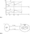
- Figure 2 shows a signal diagram of the output voltage Vout over the time when the converter stage 1 is in the burst mode.
- the output voltage oscillates between an upper voltage level Vout H and a lower voltage level Vout L , wherein the voltage increases during burst-on periods Tbon and decreases during burst-off periods Tboff.
- a difference between the upper voltage level Vout H and the lower voltage level Vout L is between 1V and 2V, for example.
- the upper voltage level Vout H is between 4.5V and 5.5V and the lower voltage level is between 3V and 4V.
- the dielectric strength of the second output capacitor 22 is adapted to the upper voltage level Vout H of the output voltage Vout in the burst mode.
- the "dielectric strength" is the maximum voltage a capacitor can withstand without being damaged.
- the dielectric strength of the second output capacitor 22 is between 5V and 7V, in particular between 5.5V and 6.5V.
- the second output capacitor 22 is a Tantalum (Ta) capacitor.
- the output voltage is regulated to a voltage level that is selected from a range that includes voltage levels higher than the upper voltage level Vout H in the burst mode.
- the dielectric strength of the first output capacitor 21 is adapted this voltage range and is higher than the maximum output voltage that may occur in the normal operating mode.
- the dielectric strength of the first output capacitor 21 is between 1.1 times and 1.5 times, in particular between 1.1 times and 1.3 times of the maximum output voltage Vout.
- the output voltage Vout in the normal operating mode, may be selected from a voltage range of between 5V and 20V and the dielectric strength of the first output capacitor 21 is selected from between 22V and 30V, in particular from between 22V and 26V.
- the dielectric strength of the second output capacitor 22 is less than 50%, less than 35%, or even less than 20% of the dielectric strength of the first output capacitor 21.
- the second output capacitor 22 is activated in the standby mode.
- the second output capacitor 22 is activated when the output voltage Vout falls below a predefined first voltage threshold Vout TH1 for the first time after the beginning of the standby mode.
- Figure 2 which, in addition to the signal diagram of the output voltage Vout, shows signal diagrams of the drive signals Sdrv23, Sdrv24 of the first and second electronic switches 23, 24.
- high signal levels of the drive signals Sdrv23, Sdrv24 represent signal levels that switch on the respective electronic switch 23, 24, and low signal levels represent signal levels that switch off the respective electronic switch 24.
- t1 denotes a time instance at which the output voltage Vout falls below the first voltage threshold Vout TH1 for the first time after the beginning of the standby mode.
- the first electronic switch 23 switches on in order to activate the second output capacitor 22.
- the first voltage threshold Vout TH1 may be selected in various ways. In each case, the first voltage threshold Vout TH1 is lower than the dielectric strength of the second output capacitor 22.
- the power supply in addition to the output nodes 25, 26, may include at least one communication port 27, wherein a communication channel can be established between the power supply and the load via this communication port 27.
- This communication port 27 may be used by the controller 3 to detect whether or not a load is connected.
- the second electronic switch 24 may be switched off at the first time instance t1, that is, when the first electronic switch 23 switches on. According to another example, the second electronic switch 24 is switched off as soon as the controller 3 detects that the load has been disconnected.
- the second output capacitor 22 is deactivated by switching off the first electronic switch 23 when the power supply changes from the standby mode to the normal operating mode.
- the first electronic switch 23 is switched off when the output voltage Vout, reaches a second voltage threshold Vout TH2 that is higher than the upper voltage level Vout H in the burst mode and lower than the dielectric strength of the second output capacitor 22.
- the first electronic switch 23 is switched off as soon as the controller 3 detects that a load has been connected to the power supply.
- the second electronic switch 24 is switched on when the first electronic switch 23 is switched off. According to another example, the second electronic switch 24 is switched on when the output voltage Vout, in the normal operating mode, has reached the setpoint voltage.
- FIG. 4 shows a block diagram of the controller 3 according to one example. It should be noted that the block diagram shown in Figure 4 illustrates the functionality of the controller 3 rather than its specific implementation.
- the controller 3 may include a digital circuit, such as a microcontroller, that executes software and analog devices, such as capacitive resistors, or the like, connected to the microcontroller.
- the individual function blocks shown in Figure 2 may be implemented using only parts of the microcontroller or may be implemented using parts of the microcontroller and using analog devices.
- the controller 3 includes a supply circuit 31 that receives the output voltage Vout and is configured to generate a supply voltage Vcc for supplying the individual circuit blocks (functional blocks) of the controller 3.
- the controller 3 further includes a feedback circuit 32 that receives the output voltage Vout and is configured to generate the feedback signal FB based on the output voltage Vout.
- the controller 3 includes a logic circuit (control circuit) 33 that also receives the output voltage Vout and is configured to drive the first and second electronic switches 23, 24.
- drive circuits 34, 35 are coupled between the logic circuit 33 and the first and second electronic switches 23, 24.
- FIG. 5 shows one example of the supply circuit 31.
- the supply circuit according to this example includes a rectifier element 311 such as a diode and a capacitor 312 connected in series with the rectifier element 311.
- the series circuit including the rectifier element 311 and the capacitor 312 receives the output voltage Vout.
- the supply voltage Vcc of the controller 3 is a voltage across the capacitor 312.
- the output voltage Vout provided by the converter stage 1 may vary within a certain voltage range.
- the supply circuit 31 may include a voltage regulator 313 (illustrated in dashed lines in Figure 3 ) configured to receive the voltage across the capacitor 312 and to generate a regulated supply voltage based Vcc on the voltage across the capacitor 312.
- FIG. 6 illustrates one example of the feedback circuit 32.
- This feedback circuit 32 includes an error amplifier 321 that receives a reference signal Sref from a reference signal source 322 and an output signal Sout, wherein the output signal Sout is dependent on the output voltage Vout.
- the output signal Sout is proportional to the output voltage Vout and is generated by a resistive voltage divider 323 that includes a first resistor 323 1 and a second resistor 323 2 which are connected in series.
- the output voltage Vout is received by the series circuit including the first resistor 323 1 and the second resistor 323 2 of the voltage divider 323, and the output signal Sout is a voltage across the second resistor 323 2 .
- the reference signal source 322 is a voltage source according to one example, so that the reference signal Sref is a reference voltage (in the following, the reference signal Sref is also referred to as reference voltage).
- the error amplifier 321 provides an error signal Serr which is dependent on a difference between the reference signal Sref and the output signal Sout. According to one example, the error signal Serr is generated such that the error signal decreases when the output voltage Vout increases, and vice versa.
- the feedback circuit 32 further includes a filter 324 that receives the error signal Serr and provides the feedback signal FB based on the error signal Serr.
- the filter 324 has a proportional-integrative (PI) characteristic or a proportional-integrative-derivative (PID) characteristic.
- the power supply in the normal operating mode, regulates the output voltage Vout and, therefore, the supply voltage Vbus received by the load in such a way that the output voltage Vout essentially equals a predefined setpoint voltage.
- this setpoint voltage is defined by the reference voltage Sref and a proportionality factor between the output signal Sout and the output voltage Vout.
- the feedback signal FB received by the power converter stage 1 essentially defines the power that is transferred from the input 11, 12 to the output 13, 14 of the converter stage 1, wherein this power is adjusted in such a way that the output voltage Vout essentially equals the desired setpoint voltage.
- the feedback signal FB is generated such that the power transferred from the input 11, 12 to the output 13, 14 increases when the feedback signal FB increases and decreases when the feedback signal FB decreases.
- the feedback signal FB is generated such that the error signal Serr is essentially zero, that is, the output signal Sout equals the reference voltage Sref and the output voltage Vout is given by the reference voltage Sref multiplied with a proportionality factor between the output signal Sout and the output voltage Vout, wherein this proportionality factor is defined by the voltage divider 323.
- the power supply in the normal operating mode, is configured to select the setpoint voltage from a predefined voltage range.
- this voltage range includes voltages from between 5V and 20V.
- the controller 3 may receive the desired setpoint voltage via the communication channel COM from the load.
- the controller 3 is configured to (a) operate the power supply such that a default level of the output voltage Vout (and the supply voltage Vbus) is generated when an input voltage Vin is received at the input 11, 12 and the presence of the load has been detected, and (b) adjust the voltage level of the output voltage Vout to a desired voltage level communicated by the load via the communication channel COM.
- the default level of the output voltage Vout is the minimum of the voltage range from which the level of the output voltage Vout can be selected.
- the controller 3 may vary the setpoint voltage by varying the proportionality factor between the output signal Sout and the output voltage Vout.
- at least one of the resistors 323 1 , 323 2 of the voltage divider 323 is a variable resistor and adjusting the proportionality factor includes adjusting a resistance of the variable resistor.
- the second resistor 323 2 is a variable resistor, wherein the resistance of this resistor is adjusted by the logic circuit 33 that is in communication with the load. In this example, decreasing the resistance of this resistor 323 2 decreases the proportionality factor between the output signal Sout and the output voltage Vout, which is equivalent to increasing the setpoint voltage.
- operating the converter stage 1 in the standby mode includes operating the converter stage 1 in the burst mode, which includes alternatingly operating the converter stage 1 in burst-on periods and burst-off periods.
- the power transferred by the converter stage 1 from the input 11, 12 to the output 13, 14 during the burst-on periods Tbon is higher than the power consumption of the controller 3 so that during the burst-on periods, the output voltage Vout increases.
- the burst-off periods Tboff in which no power is transferred from the input 11, 12 to the output 13, 14, the output voltage Vout decreases due to the power consumption of the controller 3.
- the converter stage 1 starts a burst-on period when the feedback signal FB reaches a first threshold Bon which is referred to as burst-on threshold in the following, and starts a burst-off period, when the feedback signal FB reaches a second threshold Boff, which is lower than the first threshold Bon and which is referred to as burst-off threshold in the following.
- Figure 7 schematically illustrates a signal waveform of the feedback signal FB and the output voltage Vout in the burst mode.
- the output voltage Vout increases during the burst-on periods Tbon and decreases during the burst-off periods Tboff.
- the burst-off threshold Boff is associated with the lower output voltage level Vout L and the burst-on threshold Bon is associated with the upper output voltage level Vout H .
- Figure 8 shows a state diagram that illustrates operating the power supply in the normal operating mode or the standby mode.
- State 101 in Figure 8 represents a state in which the power supply operates in the normal operating mode
- state 102 represents a state in which the power supply operates in the standby mode.
- the power supply changes from the normal operating mode 101 to the standby mode 102 when the feedback signal FB falls below a burst mode on-threshold BMon.
- this burst mode on-threshold is lower than the burst-off threshold Boff explained with reference to Figure 7 .
- the power supply operates in a burst-on mode 103 in which power is transferred from the input 11, 12 to the output 13, 14 or in a burst-off mode 104 in which no power is transferred from the input 11, 12 to the output 13, 14.
- the power supply changes from the burst-on mode 103 to the burst-off mode 104 when the feedback signal FB falls below the burst-off threshold Boff, and changes from the burst-off mode 104 to the burst-on mode 103 when the feedback signal reaches the burst-on threshold Bon.
- the converter stage 1 leaves the burst mode, that is, changes from the burst mode 102 to the normal operating mode 101, when the feedback signal FB reaches a burst mode off-threshold BMoff, which is higher than the burst-on threshold Bon.
- the converter stage 1 By operating the converter stage 1 in the normal operating mode or the standby mode dependent on the feedback signal FB, the converter stage 1 automatically changes from the normal operating mode to the standby mode, when the load is disconnected from the output 25, 26 and from the standby mode to the normal operating mode when a load is connected to the output 25, 26.
- the output voltage Vout rapidly increases because the power transferred by the converter stage 1 from the input 11, 12 to the output 13, 14 is much higher than the power consumption of the controller 3, which after disconnecting the load is the only consumer connected to the output 13, 14 of the converter stage 1.
- This rapid increase of the output voltage Vout causes the feedback signal FB to fall below the burst mode on-threshold BMon, so that the converter stage 1 enters the burst mode.
- Operating the converter stage 1 in the burst mode starts with a burst-off period in which the output voltage Vout decreases from the voltage level the output voltage Vout has reached at the end of the normal operating mode to a voltage level that is associated with the burst-on level Bon of the feedback signal FB.
- Figure 9 schematically illustrates the output voltage Vout and the feedback signal FB in a time period in which the power supply changes from the normal operating mode to the standby mode.
- the increase of the output voltage Vout before the power supply enters the standby mode is associated with a decrease of the feedback signal FB to below the burst mode on-threshold BMon.
- the controller 3 is configured to monitor the connection between the controller 3 and the load via the communication channel COM and is configured to detect that the load has been disconnected.
- the controller in response to detecting that the load has been disconnected, changes 3 the proportionality factor between the output voltage Vout and the output signal Sout from a higher level used during the normal operating mode to a lower level used in the standby mode.
- This change of the proportionality factor accelerates a decrease of the feedback signal FB to below the burst mode on-threshold BMon and therefore a deactivation of the converter stage for a first burst-off period in the burst mode.
- the converter stage 1 may be implemented in various ways.
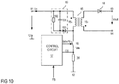
- One example for implementing the converter stage 1 is illustrated in Figure 10 .
- the converter stage 1 includes a flyback converter topology.
- the topology of the flyback converter shown in Figure 10 is commonly known, so that no detailed explanation is required in this regard.
- the flyback converter includes a transformer 15 with a primary winding 15 1 and a secondary winding 15 2 and an electronic switch 16 connected in series with the primary winding 15 1 .
- a series circuit including the primary winding 15 1 and the electronic switch 16 is connected between the input nodes 11, 12.
- the secondary winding 15 2 is coupled to the output nodes 13, 14 via a rectifier element 18.
- this rectifier element 18 is drawn as a diode in the example shown in Figure 10 .
- an active rectifier such as a synchronous rectifier (SR rectifier) may be used as well.
- SR rectifier synchronous rectifier
- a snubber circuit 19 may be coupled to the primary winding 15 1 .
- the snubber circuit 19 may include a parallel circuit including a capacitor 191 and a resistor 192 and a diode 193 connected in series with the capacitor-resistor parallel circuit.
- the snubber circuit 19 may be connected in parallel with the primary winding 15 1 .
- the snubber capacitor In the burst mode of the flyback converter, the snubber capacitor is charged during the burst on-times and discharged during the burst-off times. Each charging and discharging the snubber capacitor 191 is associated with losses. Thus, reducing the frequency at which burst-on times occur, which can be achieved by implementing the second output capacitor 22, may help to reduce losses in the standby mode.
- the converter stage 1 further includes a control circuit 17 that receives the feedback signal FB and that is configured to drive the electronic switch 16 based on the feedback signal FB.
- the control circuit 17 generates a PWM (pulse-width modulated) drive signal Sdrv16 received by the electronic switch 16.
- the control circuit 17, in the normal operating mode generates the drive signal Sdrv16 such that a duty cycle of the drive signal is dependent on the feedback signal FB, wherein the duty cycle may increase as the feedback signal FB increases. This is commonly known, so that no further explanation is required in this regard.
- the drive signal Sdrv16 may be generated with a fixed duty cycle (such as 0.5) during the burst on-periods.
- a fixed duty cycle such as 0.5
- the electronic switch 16 is deactivated.
- the converter stage 1 may operate in a current mode.
- the controller 17, for operating the converter stage 1 in the normal operating mode receives a current sense signal CS, which is proportional to a current through the electronic switch 16 and may be generated using a shunt resistor 20 connected in series with the switch 16.
- the controller 17 is configured to generate the drive signal Sdrv16 such that the electronic switch 16 switches on in accordance with a clock signal and switches off each time the current sense signal CS reaches a threshold that is proportional to the feedback signal FB. In this way, the duty cycle of the drive signal Sdrv16 is automatically adjusted to be dependent on the feedback signal FB.
Landscapes
- Engineering & Computer Science (AREA)
- Power Engineering (AREA)
- Business, Economics & Management (AREA)
- Emergency Management (AREA)
- Dc-Dc Converters (AREA)
Abstract
A control circuit, a power supply including a control circuit, and a method are disclosed. The control circuit is configured to activate a second output capacitor (22) connected in parallel with a first output capacitor (21) of a power supply when the power supply is in a normal operating mode, and deactivate the second output capacitor (22) when the power supply is in a standby mode.
Description
- This disclosure relates in general to a power supply, in particular, a switched-mode power supply.
- Switched mode power supplies are widely used in various kinds of applications. A switched mode power supply (SMPS) includes an input configured to receive an input power and an output configured to have a load connected thereto. The SMPS may operate in a normal operating mode when a load is connected to the output and provide a regulated output voltage to the load in the normal operating mode.
- Before a load is connected to the SMPS or after the load has been disconnected, the SMPS may operate in a standby mode. In the standby mode, the input power is lower than in a normal operating mode, but is not zero. In the standby mode, the input power is mainly used to supply control circuitry of the SMPS. Supplying the control circuitry in the standby mode enables the SMPS to detect when a load is connected and to enter the normal operating as soon as the load has been connected.
- It is desirable to reduce the power consumption of a switched mode power supply in the standby mode.
- One example relates to a control circuit. The control circuit is configured to activate a second output capacitor connected in parallel with a first output capacitor of a power supply when the power supply is in a normal operating mode, and deactivate the second output capacitor when the power supply is in a standby mode.
- Another example relates to a power supply. The power supply includes a converter stage having an input and an output, an output circuit connected to the output of the converter stage, and a control circuit. The output circuit includes a first output capacitor connected to the output of the converter stage, and a second output capacitor. The control circuit is configured to activate the second output capacitor when the power supply is in a normal operating mode, and deactivate the second output capacitor when the power supply is in a standby mode.
- Another example relates to a method. The method includes operating a power supply in a normal operating mode or a standby mode, wherein operating the power supply in the standby mode includes activating a second output capacitor connected in parallel with a first output capacitor of the power supply, and wherein operating the power supply in the normal operating mode comprises deactivating the second output capacitor.
- Examples are explained below with reference to the drawings. The drawings serve to illustrate certain principles, so that only aspects necessary for understanding these principles are illustrated. The drawings are not to scale. In the drawings the same reference characters denote like features.
-
Figure 1 shows a circuit diagram of the switched-mode power supply that includes a converter stage, an output circuit and a controller and that can be operated in a normal operating mode or a standby mode; -
Figure 2 shows signal diagrams that illustrate operating the power supply in the standby mode; -
Figure 3 shows signal diagrams that illustrate operating the power supply at the end of the standby mode; -
Figure 4 shows a block diagram of the controller according to one example; -
Figure 5 shows one example of a supply circuit of the controller; -
Figure 6 shows one example of a feedback circuit of the controller; -
Figure 7 shows signal diagrams that illustrate a feedback signal generated by the controller and an output voltage of the converter stage in a burst mode; -
Figure 8 shows a state diagram that illustrates operating the power supply in the normal operating mode or the standby mode; -
Figure 9 shows signal diagrams that illustrate a transfer of the power supply from the normal operating mode to the standby mode; and -
Figure 10 shows one example of the converter stage in detail. - In the following detailed description, reference is made to the accompanying drawings. The drawings form a part of the description and for the purpose of illustration show examples of how the invention may be used and implemented. It is to be understood that the features of the various embodiments described herein may be combined with each other, unless specifically noted otherwise.
-
Figure 1 shows a circuit diagram of a switched-mode power supply (SMPS) according to one example. The power supply includes a switched-mode converter stage 1 with aninput output - The power supply further includes an
output circuit 2. The output circuit includes afirst output capacitor 21 and asecond output capacitor 22. Thefirst output capacitor 21 is coupled to theoutput output capacitor 21 is coupled between afirst output node 13 and asecond output node 14 of theoutput converter stage 1. The second output capacitor is configured to be activated or deactivated. That is, thesecond output capacitor 22 is configured to be connected in parallel with thefirst output capacitor 21 or to be disconnected from thefirst output capacitor 21. For connecting thesecond output capacitor 22 in parallel with thefirst output capacitor 21 or for disconnecting thesecond output capacitor 22 from thefirst output capacitor 21, theoutput circuit 2 includes a firstelectronic switch 23. This firstelectronic switch 23 is connected in series with thesecond output capacitor 22, wherein the series circuit including thesecond output capacitor 22 and the firstelectronic switch 23 is connected in parallel with thefirst output capacitor 21. The circuit with thefirst output capacitor 21, thesecond output capacitor 22 and the firstelectronic switch 23 is also referred to asoutput capacitor circuit 20 in the following. - Referring to
Figure 1 , theoutput circuit 2 further includes anoutput Figure 1 ). A secondelectronic switch 24 is connected between theoutput capacitor circuit 20 and theoutput electronic switch 24 can be switched on (activated) or switched off (deactivated). When the secondelectronic switch 24 is switched on, theoutput capacitor circuit 20 is connected to theoutput output electronic switch 24 is negligible). When the secondelectronic switch 24 is switched off, theoutput capacitor circuit 20 is disconnected from theoutput converter stage 1 to the load is interrupted. - Just for the purpose of illustration, in the example shown in
Figure 1 , the secondelectronic switch 24 is connected between thefirst output node 13 of theconverter stage 1 and the afirst output node 25 of theoutput circuit 2. This, however, is only an example. According to another example (not shown), the secondelectronic switch 24 is connected between thesecond output node 14 of theconverter stage 1 and thesecond output node 26 of theoutput circuit 2. In each case, a power transfer between theconverter stage 1 and theoutput output circuit 2 is interrupted when the secondelectronic switch 24 is switched off. - Any kind of conventional electronic switch may be used to implement the first and second
electronic switch electronic switch 24 is a bidirectional blocking electronic switch that includes two MOSFETs in a series configuration such that body diodes of the two MOSFETs are in a back-to-back configuration. - In the power supply shown in
Figure 1 , theinput converter stage 1 forms an input of the power supply and theoutput output circuit 2 forms an output of the power supply. - Optionally, the
output circuit 2 further includes athird output capacitor 28 that is connected between theoutput nodes first output capacitor 21. According to one example, the capacitance of thethird output capacitor 28 is less than 10%, less than 5%, or less than 2% of the capacitance of thefirst output capacitor 21. The capacitance of the first output capacitor is between 30 microfarads (µF) and 100 microfarads, for example. - According to one example, the capacitance of the
second output capacitor 21 is higher than the capacitance of thefirst output capacitor 21. According to one example, the capacitance of thesecond output capacitor 22 is at least 2 times, at least 3 times, at least 5 times, or at least 10 times the capacitance of thefirst output capacitor 21. The capacitance of thesecond output capacitor 22 is selected from between 100 microfarads (µF) and 1000 microfarads (µF) (=1 millifarad), for example. - The power supply shown in
Figure 1 may be part of a so-called USB (Universal Serial Bus) PD (Power Delivery) device. In addition to the power supply, which receives a direct input voltage Vin, the USB PD device may include a PFC converter (not shown) that receives an alternating grid voltage and provides the DC input voltage Vin. - Referring to
Figure 1 , the power supply further includes a control circuit (controller) 3. Thecontroller 3 receives the output voltage Vout and is configured to generate a feedback signal FB based on the output voltage Vout. The feedback signal FB is received by theconverter stage 1. According to one example, theconverter stage 1 includes a galvanic isolation between theinput output controller 3 and theconverter stage 1, wherein the coupler 4 is configured to transmit the feedback signal FB from thecontroller 3 to theconverter stage 1 via the galvanic isolation included in theconverter stage 1. According to one example, the coupler 4 is an opto-coupler an inductive coupler, a capacitive coupler, or the like. - The
controller 3 is configured to activate and deactivate thesecond output capacitor 22. That is, thecontroller 3 is configured to control operation of the firstelectronic switch 23 that either connects thesecond output capacitor 22 in parallel with thefirst output capacitor 21, or disconnects thesecond output capacitor 22 from thefirst output capacitor 21. For controlling operation of the firstelectronic switch 23,controller 3 is configured to generate a first drive signal Sdrv23 that is configured to switch on or off the firstelectronic switch 23. Thecontroller 3 may also be configured to control operation of the secondelectronic switch 24 of theoutput circuit 2. That is, thecontroller 3 may be configured to provide a second drive signal Sdrv24 that is configured to switch on or off the secondelectronic switch 24. Operation of thecontroller 3 for controlling the first and secondelectronic switches - According to one example, the power supply is configured to operate in a first operating mode, which is also referred to as normal operating mode in the following, or a second operating mode, which is also referred to as standby mode in the following. The power supply may operate in the normal operating mode when the load is connected to the
output - In the normal operating mode,
controller 3 switches off the firstelectronic switch 23 and switches on the secondelectronic switch 24. Thus, in the normal operating mode, only thefirst output capacitor 21 contributes to an output capacitance of the power supply and the supply voltage Vbus received by the load essentially equals the output voltage Vout of theconverter stage 1. Furthermore, in the normal operating mode, the power supply regulates the output voltage Vout and, therefore, the supply voltage Vbus received by the load, in such a way that the output voltage Vout essentially equals a predefined setpoint voltage. This is explained in detail herein further below. In the normal operating mode, theconverter stage 1 supplies both, the load and thecontroller 3 with electrical power required to ensure a proper operation of the load and thecontroller 3. According to one example, the power consumption of the load is significantly higher than the power consumption of thecontroller 3. According to one example, the power consumption of the load is higher than 1W and the power consumption of thecontroller 3 is lower than 1W. - In the standby mode,
controller 3 connects thesecond output capacitor 22 in parallel to thefirst output capacitor 21 by switching on the firstelectronic switch 23 and switches off the secondelectronic switch 24. Thus, in the standby mode, thefirst output capacitor 21 and thesecond output capacitor 22 contribute to the output capacitance of the power supply. The output capacitance in the standby mode is given by the parallel circuit of the first andsecond output capacitors controller 3 is supplied by theconverter stage 1. - According to one example, operating the power supply in the standby mode includes operating the
converter stage 1 in a burst mode. Operating theconverter stage 1 in the burst mode includes alternatingly operating theconverter stage 1 in burst-on periods and burst-off periods. Operating theconverter stage 1 in the burst-on periods includes transferring power from theinput output output capacitor circuit 20. Operating theconverter stage 1 in the burst-off periods includes deactivating theconverter stage 1 so that no power is transferred from theinput output converter stage 1 from theinput output controller 3 so that during the burst-on periods, the output voltage Vout increases. During the burst-off periods, in which no power is transferred from theinput output controller 3. - This is illustrated in
Figure 2 which shows a signal diagram of the output voltage Vout over the time when theconverter stage 1 is in the burst mode. As can be seen from Figure, the output voltage oscillates between an upper voltage level VoutH and a lower voltage level VoutL, wherein the voltage increases during burst-on periods Tbon and decreases during burst-off periods Tboff. - A difference between the upper voltage level VoutH and the lower voltage level VoutL is between 1V and 2V, for example. According to one example, the upper voltage level VoutH is between 4.5V and 5.5V and the lower voltage level is between 3V and 4V.
- Operating the
converter stage 1 in the burst-on periods, that is, transferring power from theinput output second output capacitor 22 in parallel with thefirst output capacitor 21 helps to reduce these power losses. Increasing the output capacitance in the standby mode increases a duration of the burst-off periods Tboff, as compared to a scenario in which thesecond output capacitor 22 is omitted. Thus, theconverter stage 1 is activated less often within a given time period. Operating the power supply in burst-on periods less frequently helps to reduce power losses, which will be explained in detail herein further below. - The dielectric strength of the
second output capacitor 22 is adapted to the upper voltage level VoutH of the output voltage Vout in the burst mode. The "dielectric strength" is the maximum voltage a capacitor can withstand without being damaged. According to one example, the dielectric strength of thesecond output capacitor 22 is between 5V and 7V, in particular between 5.5V and 6.5V. According to one example, thesecond output capacitor 22 is a Tantalum (Ta) capacitor. - According to one example, in the normal operating mode, the output voltage is regulated to a voltage level that is selected from a range that includes voltage levels higher than the upper voltage level VoutH in the burst mode. The dielectric strength of the
first output capacitor 21 is adapted this voltage range and is higher than the maximum output voltage that may occur in the normal operating mode. According to one example, the dielectric strength of thefirst output capacitor 21 is between 1.1 times and 1.5 times, in particular between 1.1 times and 1.3 times of the maximum output voltage Vout. - According to one example, the output voltage Vout, in the normal operating mode, may be selected from a voltage range of between 5V and 20V and the dielectric strength of the
first output capacitor 21 is selected from between 22V and 30V, in particular from between 22V and 26V. - According to one example, the dielectric strength of the
second output capacitor 22 is less than 50%, less than 35%, or even less than 20% of the dielectric strength of thefirst output capacitor 21. - Referring to the above, the
second output capacitor 22 is activated in the standby mode. According to one example, thesecond output capacitor 22 is activated when the output voltage Vout falls below a predefined first voltage threshold VoutTH1 for the first time after the beginning of the standby mode. This is illustrated inFigure 2 which, in addition to the signal diagram of the output voltage Vout, shows signal diagrams of the drive signals Sdrv23, Sdrv24 of the first and secondelectronic switches electronic switch electronic switch 24. - In
Figure 2 , t1 denotes a time instance at which the output voltage Vout falls below the first voltage threshold VoutTH1 for the first time after the beginning of the standby mode. At this time instance, the firstelectronic switch 23 switches on in order to activate thesecond output capacitor 22. The first voltage threshold VoutTH1 may be selected in various ways. In each case, the first voltage threshold VoutTH1 is lower than the dielectric strength of thesecond output capacitor 22. - (a) According to one example, the first voltage threshold VoutTH1 is selected such that the output voltage Vout can reach the first voltage threshold VoutTH1 only when the power supply is in the standby mode, which may be achieved by selecting the first voltage threshold VoutTH1 from a range of between the lower voltage level VoutL and the upper voltage level VoutH. In this case, a decision on whether to switch on the first
electronic switch 23 may be based only on the output voltage Vout. - (b) According to another example, the first voltage threshold VoutTH1 is selected such that the output voltage Vout can reach the first voltage threshold VoutTH1 in the normal operating mode and in the standby mode. Thus, a decision on whether to switch on the first
electronic switch 23 cannot only be based on the output voltage Vout, so that further information is required. This further information may include information on the load status, that is, whether or not a load is connected to the power supply. According to one example, thecontroller 3 is configured to detect whether or not the load is connected to the power supply and thecontroller 3 is configured to switch on the firstelectronic switch 23 when no load is connected and the output voltage falls below the first voltage threshold VoutTH1. - Referring to
Figure 1 , the power supply, in addition to theoutput nodes communication port 27, wherein a communication channel can be established between the power supply and the load via thiscommunication port 27. Thiscommunication port 27 may be used by thecontroller 3 to detect whether or not a load is connected. - Referring to
Figure 2 , the secondelectronic switch 24 may be switched off at the first time instance t1, that is, when the firstelectronic switch 23 switches on. According to another example, the secondelectronic switch 24 is switched off as soon as thecontroller 3 detects that the load has been disconnected. - The
second output capacitor 22 is deactivated by switching off the firstelectronic switch 23 when the power supply changes from the standby mode to the normal operating mode. According to one example, illustrated inFigure 3 , the firstelectronic switch 23 is switched off when the output voltage Vout, reaches a second voltage threshold VoutTH2 that is higher than the upper voltage level VoutH in the burst mode and lower than the dielectric strength of thesecond output capacitor 22. - According to another example, the first
electronic switch 23 is switched off as soon as thecontroller 3 detects that a load has been connected to the power supply. - According to one example the second
electronic switch 24 is switched on when the firstelectronic switch 23 is switched off. According to another example, the secondelectronic switch 24 is switched on when the output voltage Vout, in the normal operating mode, has reached the setpoint voltage. -
Figure 4 shows a block diagram of thecontroller 3 according to one example. It should be noted that the block diagram shown inFigure 4 illustrates the functionality of thecontroller 3 rather than its specific implementation. Thecontroller 3 may include a digital circuit, such as a microcontroller, that executes software and analog devices, such as capacitive resistors, or the like, connected to the microcontroller. The individual function blocks shown inFigure 2 may be implemented using only parts of the microcontroller or may be implemented using parts of the microcontroller and using analog devices. - Referring to
Figure 4 , thecontroller 3 includes asupply circuit 31 that receives the output voltage Vout and is configured to generate a supply voltage Vcc for supplying the individual circuit blocks (functional blocks) of thecontroller 3. Thecontroller 3 further includes afeedback circuit 32 that receives the output voltage Vout and is configured to generate the feedback signal FB based on the output voltage Vout. Furthermore, thecontroller 3 includes a logic circuit (control circuit) 33 that also receives the output voltage Vout and is configured to drive the first and secondelectronic switches circuits 34, 35 (illustrated in dashed lines inFigure 2 ) are coupled between thelogic circuit 33 and the first and secondelectronic switches -
Figure 5 shows one example of thesupply circuit 31. The supply circuit according to this example includes arectifier element 311 such as a diode and acapacitor 312 connected in series with therectifier element 311. The series circuit including therectifier element 311 and thecapacitor 312 receives the output voltage Vout. The supply voltage Vcc of thecontroller 3 is a voltage across thecapacitor 312. According to one example, the output voltage Vout provided by theconverter stage 1 may vary within a certain voltage range. Thus, according to one example, thesupply circuit 31 may include a voltage regulator 313 (illustrated in dashed lines inFigure 3 ) configured to receive the voltage across thecapacitor 312 and to generate a regulated supply voltage based Vcc on the voltage across thecapacitor 312. -
Figure 6 illustrates one example of thefeedback circuit 32. Thisfeedback circuit 32 includes anerror amplifier 321 that receives a reference signal Sref from a reference signal source 322 and an output signal Sout, wherein the output signal Sout is dependent on the output voltage Vout. According to one example, the output signal Sout is proportional to the output voltage Vout and is generated by aresistive voltage divider 323 that includes afirst resistor 3231 and asecond resistor 3232 which are connected in series. The output voltage Vout is received by the series circuit including thefirst resistor 3231 and thesecond resistor 3232 of thevoltage divider 323, and the output signal Sout is a voltage across thesecond resistor 3232. The reference signal source 322 is a voltage source according to one example, so that the reference signal Sref is a reference voltage (in the following, the reference signal Sref is also referred to as reference voltage). Theerror amplifier 321 provides an error signal Serr which is dependent on a difference between the reference signal Sref and the output signal Sout. According to one example, the error signal Serr is generated such that the error signal decreases when the output voltage Vout increases, and vice versa. - Referring to
Figure 6 , thefeedback circuit 32 further includes a filter 324 that receives the error signal Serr and provides the feedback signal FB based on the error signal Serr. According to one example, the filter 324 has a proportional-integrative (PI) characteristic or a proportional-integrative-derivative (PID) characteristic. - Referring to the above the power supply, in the normal operating mode, regulates the output voltage Vout and, therefore, the supply voltage Vbus received by the load in such a way that the output voltage Vout essentially equals a predefined setpoint voltage. According to one example, this setpoint voltage is defined by the reference voltage Sref and a proportionality factor between the output signal Sout and the output voltage Vout. In the normal operating mode, the feedback signal FB received by the
power converter stage 1 essentially defines the power that is transferred from theinput output converter stage 1, wherein this power is adjusted in such a way that the output voltage Vout essentially equals the desired setpoint voltage. - According to one example, the feedback signal FB is generated such that the power transferred from the
input output voltage divider 323. - According to one example, the power supply, in the normal operating mode, is configured to select the setpoint voltage from a predefined voltage range. According to one example, this voltage range includes voltages from between 5V and 20V. The
controller 3 may receive the desired setpoint voltage via the communication channel COM from the load. - According to one example, the
controller 3 is configured to (a) operate the power supply such that a default level of the output voltage Vout (and the supply voltage Vbus) is generated when an input voltage Vin is received at theinput - The
controller 3 may vary the setpoint voltage by varying the proportionality factor between the output signal Sout and the output voltage Vout. According to one example, at least one of theresistors voltage divider 323 is a variable resistor and adjusting the proportionality factor includes adjusting a resistance of the variable resistor. According to one example, thesecond resistor 3232 is a variable resistor, wherein the resistance of this resistor is adjusted by thelogic circuit 33 that is in communication with the load. In this example, decreasing the resistance of thisresistor 3232 decreases the proportionality factor between the output signal Sout and the output voltage Vout, which is equivalent to increasing the setpoint voltage. - Referring to the above, operating the
converter stage 1 in the standby mode includes operating theconverter stage 1 in the burst mode, which includes alternatingly operating theconverter stage 1 in burst-on periods and burst-off periods. The power transferred by theconverter stage 1 from theinput output controller 3 so that during the burst-on periods, the output voltage Vout increases. During the burst-off periods Tboff, in which no power is transferred from theinput output controller 3. Thus, during the burst-on periods Tbon, the feedback signal FB decreases, and during the burst-off periods Tboff, the feedback signal FB increases. According to one example, in the burst mode, theconverter stage 1 starts a burst-on period when the feedback signal FB reaches a first threshold Bon which is referred to as burst-on threshold in the following, and starts a burst-off period, when the feedback signal FB reaches a second threshold Boff, which is lower than the first threshold Bon and which is referred to as burst-off threshold in the following. - This is schematically illustrated in
Figure 7 , which schematically illustrates a signal waveform of the feedback signal FB and the output voltage Vout in the burst mode. Referring toFigure 7 , and as discussed above, the output voltage Vout increases during the burst-on periods Tbon and decreases during the burst-off periods Tboff. The burst-off threshold Boff is associated with the lower output voltage level VoutL and the burst-on threshold Bon is associated with the upper output voltage level VoutH. -
Figure 8 shows a state diagram that illustrates operating the power supply in the normal operating mode or the standby mode.State 101 inFigure 8 represents a state in which the power supply operates in the normal operating mode, andstate 102 represents a state in which the power supply operates in the standby mode. According to one example, the power supply changes from thenormal operating mode 101 to thestandby mode 102 when the feedback signal FB falls below a burst mode on-threshold BMon. According to one example, this burst mode on-threshold is lower than the burst-off threshold Boff explained with reference toFigure 7 . Within thestandby mode 102, the power supply operates in a burst-onmode 103 in which power is transferred from theinput output off mode 104 in which no power is transferred from theinput output Figure 7 , the power supply changes from the burst-onmode 103 to the burst-off mode 104 when the feedback signal FB falls below the burst-off threshold Boff, and changes from the burst-off mode 104 to the burst-onmode 103 when the feedback signal reaches the burst-on threshold Bon. - Referring to
Figure 8 , theconverter stage 1 leaves the burst mode, that is, changes from theburst mode 102 to thenormal operating mode 101, when the feedback signal FB reaches a burst mode off-threshold BMoff, which is higher than the burst-on threshold Bon. - By operating the
converter stage 1 in the normal operating mode or the standby mode dependent on the feedback signal FB, theconverter stage 1 automatically changes from the normal operating mode to the standby mode, when the load is disconnected from theoutput output converter stage 1 is in the normal operating mode and the load is disconnected, the output voltage Vout rapidly increases because the power transferred by theconverter stage 1 from theinput output controller 3, which after disconnecting the load is the only consumer connected to theoutput converter stage 1. This rapid increase of the output voltage Vout causes the feedback signal FB to fall below the burst mode on-threshold BMon, so that theconverter stage 1 enters the burst mode. Operating theconverter stage 1 in the burst mode starts with a burst-off period in which the output voltage Vout decreases from the voltage level the output voltage Vout has reached at the end of the normal operating mode to a voltage level that is associated with the burst-on level Bon of the feedback signal FB. - This is illustrated in
Figure 9 which schematically illustrates the output voltage Vout and the feedback signal FB in a time period in which the power supply changes from the normal operating mode to the standby mode. As explained above, the increase of the output voltage Vout before the power supply enters the standby mode is associated with a decrease of the feedback signal FB to below the burst mode on-threshold BMon. According to one example, thecontroller 3 is configured to monitor the connection between thecontroller 3 and the load via the communication channel COM and is configured to detect that the load has been disconnected. According to one example, in response to detecting that the load has been disconnected, the controller changes 3 the proportionality factor between the output voltage Vout and the output signal Sout from a higher level used during the normal operating mode to a lower level used in the standby mode. This change of the proportionality factor accelerates a decrease of the feedback signal FB to below the burst mode on-threshold BMon and therefore a deactivation of the converter stage for a first burst-off period in the burst mode. - The
converter stage 1 may be implemented in various ways. One example for implementing theconverter stage 1 is illustrated inFigure 10 . In this example, theconverter stage 1 includes a flyback converter topology. The topology of the flyback converter shown inFigure 10 is commonly known, so that no detailed explanation is required in this regard. Referring toFigure 10 , the flyback converter includes atransformer 15 with a primary winding 151 and a secondary winding 152 and anelectronic switch 16 connected in series with the primary winding 151. A series circuit including the primary winding 151 and theelectronic switch 16 is connected between theinput nodes output nodes rectifier element 18. Just for the purpose of illustration, thisrectifier element 18 is drawn as a diode in the example shown inFigure 10 . Of course, an active rectifier such as a synchronous rectifier (SR rectifier) may be used as well. - Referring to
Figure 10 , asnubber circuit 19 may be coupled to the primary winding 151. Thesnubber circuit 19 may include a parallel circuit including acapacitor 191 and aresistor 192 and adiode 193 connected in series with the capacitor-resistor parallel circuit. Thesnubber circuit 19 may be connected in parallel with the primary winding 151. - In the burst mode of the flyback converter, the snubber capacitor is charged during the burst on-times and discharged during the burst-off times. Each charging and discharging the
snubber capacitor 191 is associated with losses. Thus, reducing the frequency at which burst-on times occur, which can be achieved by implementing thesecond output capacitor 22, may help to reduce losses in the standby mode. - Referring to
Figure 10 , theconverter stage 1 further includes acontrol circuit 17 that receives the feedback signal FB and that is configured to drive theelectronic switch 16 based on the feedback signal FB. Thecontrol circuit 17 generates a PWM (pulse-width modulated) drive signal Sdrv16 received by theelectronic switch 16. According to one example, thecontrol circuit 17, in the normal operating mode, generates the drive signal Sdrv16 such that a duty cycle of the drive signal is dependent on the feedback signal FB, wherein the duty cycle may increase as the feedback signal FB increases. This is commonly known, so that no further explanation is required in this regard. - In the burst mode, the drive signal Sdrv16 may be generated with a fixed duty cycle (such as 0.5) during the burst on-periods. During the burst-off periods, the
electronic switch 16 is deactivated. - The
converter stage 1 may operate in a current mode. In this operating mode, thecontroller 17, for operating theconverter stage 1 in the normal operating mode, receives a current sense signal CS, which is proportional to a current through theelectronic switch 16 and may be generated using ashunt resistor 20 connected in series with theswitch 16. In this example, thecontroller 17 is configured to generate the drive signal Sdrv16 such that theelectronic switch 16 switches on in accordance with a clock signal and switches off each time the current sense signal CS reaches a threshold that is proportional to the feedback signal FB. In this way, the duty cycle of the drive signal Sdrv16 is automatically adjusted to be dependent on the feedback signal FB. - Although the present disclosure is not so limited, the following numbered examples demonstrate one or more aspects of the disclosure.
- Example 1 - A control circuit configured to activate a second output capacitor connected in parallel with a first output capacitor of a power supply when the power supply is in a normal operating mode, and deactivate the second output capacitor when the power supply is in a standby mode.
- Example 2 - The control circuit according to example 1, wherein the control circuit is further configured to control operation of the power supply such that the power supply operates in the normal mode or the standby mode.
- Example 3 - The control circuit according to example 2, wherein the control circuit is configured, in the standby mode, to operate the power supply in a burst mode.
- Example 4 - A power supply, including: a converter stage having an input and an output; an output circuit connected to the output of the converter stage; and a control circuit according to any one of examples 1 to 4, wherein the output circuit includes a first output capacitor connected to the output of the converter stage, and a second output capacitor.
- Example 5 - The power supply of example 4, wherein a dielectric strength of the second output capacitor is less than 50%, less than 35%, or less than 20% of the dielectric strength of the first output capacitor.
- Example 6 - The power supply of example 4 or 5, wherein a capacitance of the second output capacitor is at least 2 times, at least 3 times, at least 5 times, or at least 10 times the capacitance of the first output capacitor.
- Example 7 - The power supply according to any one of the preceding examples, wherein the output circuit further includes: a first electronic switch connected in series with the second output capacitor and configured to be controlled by the control circuit to activate or deactivate the second output capacitor.
- Example 8 - The power supply according to any one of the preceding examples, wherein the output circuit further includes: a second electronic switch connected between the first output capacitor and the output and configured to be controlled by the control circuit.
- Example 9 - The power supply of any one of examples 4 to 8, wherein the control circuit is further configured to monitor an output voltage of the converter stage and to activate the second output capacitor dependent on the output voltage.
- Example 10 - The power supply of example 9, wherein the control circuit is further configured to detect the presence of a load connected to the output circuit and to activate the second output capacitor dependent on the presence of the load.
- Example 11 - The power supply of example 9, wherein the control circuit includes a communication port configured to allow the control circuit to communicate with a load, and wherein the control circuit is configured to detect the presence of the load by monitoring the communication port.
- Example 12 - The power supply any one of the preceding examples, wherein the control circuit is configured to receive an output voltage from the converter stage and generate an internal supply voltage based on the output voltage.
- Example 13 - The power supply any one of examples 8 to 12, wherein the control circuit is configured to switch on the second electronic switch in the normal operating mode and switch off the second electronic switch in the standby mode.
- Example 14 - A method, including: operating a power supply in a normal operating mode or a standby mode, wherein operating the power supply in the standby mode includes activating a second output capacitor connected in parallel with a first output capacitor of the power supply, and wherein operating the power supply in the normal operating mode includes deactivating the second output capacitor.
- Example 15 - The method of example 14, further including: detecting the presence of a load connected to the power supply, and operating the power supply in the normal mode when the presence of a load is detected and in the standby mode when the presence of a load is not detected.
Claims (15)
- A control circuit configured to
activate a second output capacitor (22) connected in parallel with a first output capacitor (21) of a power supply when the power supply is in a normal operating mode, and
deactivate the second output capacitor (22) when the power supply is in a standby mode. - The control circuit according to claim 1, wherein the control circuit (3) is further configured to control operation of the power supply such that the power supply operates in the normal mode or the standby mode.
- The control circuit according to claim 2, wherein the control circuit (3) is configured, in the standby mode, to operate the power supply in a burst mode.
- A power supply, comprising:a converter stage (1) having an input (11, 12) and an output (13, 14);an output circuit (2) connected to the output (13, 14) of the converter stage (1); anda control circuit (3) according to any one of claims 1 to 3,wherein the output circuit (2) comprises a first output capacitor (21) connected to the output (13, 14) of the converter stage (1), and a second output capacitor (22).
- The power supply of claim 4,
wherein a dielectric strength of the second output capacitor (22) is less than 50% 50%, less than 35%, or less than 20% of the dielectric strength of the first output capacitor (21). - The power supply of claim 4 or 5,
wherein a capacitance of the second output capacitor (22) is at least 2 times, at least 3 times, at least 5 times, or at least 10 times the capacitance of the first output capacitor (21). - The power supply according to any one of the preceding claims, wherein the output circuit (2) further comprises:
a first electronic switch (23) connected in series with the second output capacitor (22) and configured to be controlled by the control circuit (3) to activate or deactivate the second output capacitor (22). - The power supply according to any one of the preceding claims, wherein the output circuit (2) further comprises:
a second electronic switch (24) connected between the first output capacitor (21) and the output (25, 26) and configured to be controlled by the control circuit (3). - The power supply of any one of claims 4 to 8,
wherein the control circuit (3) is further configured to monitor an output voltage (Vout) of the converter stage (1) and to activate the second output capacitor (22) dependent on the output voltage. - The power supply of claim 9,
wherein the control circuit (3) is further configured to detect the presence of a load connected to the output circuit and to activate the second output capacitor (22) dependent on the presence of the load. - The power supply of claim 9,
wherein the control circuit comprises a communication port (27) configured to allow the control circuit (3) to communicate with a load, and
wherein the control circuit is configured to detect the presence of the load by monitoring the communication port (27). - The power supply any one of the preceding claims,
wherein the control circuit (3) is configured to receive an output voltage (Vout) from the converter stage (1) and generate an internal supply voltage (Vcc) based on the output voltage (Vout). - The power supply any one of claims 8 to 12,
wherein the control circuit (3) is configured to switch on the second electronic switch (24) in the normal operating mode and switch off the second electronic switch (24) in the standby mode. - A method, comprising:operating a power supply in a normal operating mode or a standby mode,wherein operating the power supply in the standby mode comprises activating a second output capacitor (22) connected in parallel with a first output capacitor (21) of the power supply, andwherein operating the power supply in the normal operating mode comprises deactivating the second output capacitor (22).
- The method of claim 14, further comprising:detecting the presence of a load connected to the power supply, andoperating the power supply in the normal mode when the presence of a load is detected and in the standby mode when the presence of a load is not detected.
Priority Applications (3)
| Application Number | Priority Date | Filing Date | Title |
|---|---|---|---|
| EP21154050.5A EP4037169A1 (en) | 2021-01-28 | 2021-01-28 | Control circuit for a power suuply and power supply with reduced standby power losses |
| CN202210055013.3A CN114825568A (en) | 2021-01-28 | 2022-01-18 | Control circuit, power supply and method for operating a power supply |
| US17/577,697 US11901802B2 (en) | 2021-01-28 | 2022-01-18 | Control circuit for a power supply and power supply with reduced standby power losses |
Applications Claiming Priority (1)
| Application Number | Priority Date | Filing Date | Title |
|---|---|---|---|
| EP21154050.5A EP4037169A1 (en) | 2021-01-28 | 2021-01-28 | Control circuit for a power suuply and power supply with reduced standby power losses |
Publications (1)
| Publication Number | Publication Date |
|---|---|
| EP4037169A1 true EP4037169A1 (en) | 2022-08-03 |
Family
ID=74346995
Family Applications (1)
| Application Number | Title | Priority Date | Filing Date |
|---|---|---|---|
| EP21154050.5A Pending EP4037169A1 (en) | 2021-01-28 | 2021-01-28 | Control circuit for a power suuply and power supply with reduced standby power losses |
Country Status (3)
| Country | Link |
|---|---|
| US (1) | US11901802B2 (en) |
| EP (1) | EP4037169A1 (en) |
| CN (1) | CN114825568A (en) |
Families Citing this family (2)
| Publication number | Priority date | Publication date | Assignee | Title |
|---|---|---|---|---|
| JP7342900B2 (en) * | 2021-02-26 | 2023-09-12 | 株式会社村田製作所 | voltage converter |
| US12308693B2 (en) * | 2023-01-20 | 2025-05-20 | Datalogic Ip Tech S.R.L. | Power supply having low standby power consumption |
Citations (7)
| Publication number | Priority date | Publication date | Assignee | Title |
|---|---|---|---|---|
| JPH11252701A (en) * | 1998-02-25 | 1999-09-17 | Toshiba Corp | Derailment compensator for vehicle power supply |
| EP1178585A2 (en) * | 2000-08-04 | 2002-02-06 | Matsushita Electric Industrial Co., Ltd. | Power source system |
| US20090103337A1 (en) * | 2007-10-17 | 2009-04-23 | Power Integrations, Inc. | Method and apparatus to reduce the volume required for bulk capacitance in a power supply |
| JP2009278822A (en) * | 2008-05-16 | 2009-11-26 | Nanao Corp | Electronic equipment |
| WO2013048535A1 (en) * | 2011-10-01 | 2013-04-04 | Intel Corporation | Voltage regulator |
| US20170294830A1 (en) * | 2016-04-11 | 2017-10-12 | Futurewei Technologies, Inc. | Method and Apparatus for Filtering A Rectified Voltage Signal |
| CN110289756A (en) * | 2019-06-26 | 2019-09-27 | 海矽微(厦门)电子有限公司 | An electrical appliance and its standby power supply |
Family Cites Families (8)
| Publication number | Priority date | Publication date | Assignee | Title |
|---|---|---|---|---|
| US7928705B2 (en) * | 2008-03-12 | 2011-04-19 | Sony Ericsson Mobile Communications Ab | Switched mode voltage converter with low-current mode and methods of performing voltage conversion with low-current mode |
| CN101674004B (en) * | 2009-10-01 | 2012-09-19 | 英飞特电子(杭州)有限公司 | Circuit for improving light-load power factor of power supply |
| KR20150049962A (en) * | 2013-10-31 | 2015-05-08 | 삼성전기주식회사 | Power supply apparatus and controlling method thereof |
| US9917518B2 (en) * | 2014-04-24 | 2018-03-13 | Semiconductor Components Industries, Llc | Method and circuit of detecting attachment and detachment between a portable device and a power converter |
| PL226645B1 (en) * | 2014-05-22 | 2017-08-31 | Wb Electronics Spółka Akcyjna | Pulse feeder |
| US9882472B2 (en) * | 2014-09-25 | 2018-01-30 | Intel Corporation | Techniques for power supply topologies with capacitance management to reduce power loss associated with charging and discharging when cycling between power states |
| EP4109713A1 (en) * | 2021-06-21 | 2022-12-28 | Infineon Technologies Austria AG | Circuit and method for extending the hold-up time |
| EP4109712A1 (en) * | 2021-06-21 | 2022-12-28 | Infineon Technologies Austria AG | Circuit and method for extending the hold-up time |
-
2021
- 2021-01-28 EP EP21154050.5A patent/EP4037169A1/en active Pending
-
2022
- 2022-01-18 CN CN202210055013.3A patent/CN114825568A/en active Pending
- 2022-01-18 US US17/577,697 patent/US11901802B2/en active Active
Patent Citations (7)
| Publication number | Priority date | Publication date | Assignee | Title |
|---|---|---|---|---|
| JPH11252701A (en) * | 1998-02-25 | 1999-09-17 | Toshiba Corp | Derailment compensator for vehicle power supply |
| EP1178585A2 (en) * | 2000-08-04 | 2002-02-06 | Matsushita Electric Industrial Co., Ltd. | Power source system |
| US20090103337A1 (en) * | 2007-10-17 | 2009-04-23 | Power Integrations, Inc. | Method and apparatus to reduce the volume required for bulk capacitance in a power supply |
| JP2009278822A (en) * | 2008-05-16 | 2009-11-26 | Nanao Corp | Electronic equipment |
| WO2013048535A1 (en) * | 2011-10-01 | 2013-04-04 | Intel Corporation | Voltage regulator |
| US20170294830A1 (en) * | 2016-04-11 | 2017-10-12 | Futurewei Technologies, Inc. | Method and Apparatus for Filtering A Rectified Voltage Signal |
| CN110289756A (en) * | 2019-06-26 | 2019-09-27 | 海矽微(厦门)电子有限公司 | An electrical appliance and its standby power supply |
Non-Patent Citations (1)
| Title |
|---|
| YUNGTAEK JANG ET AL: "Light-Load Efficiency Optimization Method", IEEE TRANSACTIONS ON POWER ELECTRONICS, INSTITUTE OF ELECTRICAL AND ELECTRONICS ENGINEERS, USA, vol. 25, no. 1, 1 January 2010 (2010-01-01), pages 67 - 74, XP011282317, ISSN: 0885-8993, DOI: 10.1109/TPEL.2009.2024419 * |
Also Published As
| Publication number | Publication date |
|---|---|
| US11901802B2 (en) | 2024-02-13 |
| US20220239216A1 (en) | 2022-07-28 |
| CN114825568A (en) | 2022-07-29 |
Similar Documents
| Publication | Publication Date | Title |
|---|---|---|
| US20230133307A1 (en) | Auxiliary Power Supply Apparatus and Method for Isolated Power Converters | |
| KR101850153B1 (en) | Dc/dc converter, and power supply and electronic device using the same | |
| US7787261B2 (en) | Intermediate bus architecture with a quasi-regulated bus converter | |
| US6295214B1 (en) | Switching power supply unit | |
| US8885370B2 (en) | Current-fed isolation converter | |
| EP2876798B1 (en) | Synchronous rectifier controller | |
| US8823353B2 (en) | Power controller with smooth transition to pulse skipping | |
| TW202234811A (en) | Reduced power consumption for llc resonant converter under light load | |
| US11979090B2 (en) | Power converter controller with branch switch | |
| US11606037B2 (en) | Detection circuit and switching converter | |
| WO2006095328A2 (en) | Switched mode power converter and method of operation thereof | |
| CN113131744A (en) | Auxiliary converter for providing operating power for controller | |
| CN116260319B (en) | Power converter and power switch controller for power converter | |
| US8503195B1 (en) | System and method for zero volt switching of half bridge converters during startup and short circuit conditions | |
| US11901802B2 (en) | Control circuit for a power supply and power supply with reduced standby power losses | |
| US9564819B2 (en) | Switching power supply circuit | |
| US7724555B1 (en) | Power converter with synchronous rectification and digital current sharing | |
| US11637489B2 (en) | Isolated DC/DC converter and AC/DC converter | |
| CN115811219A (en) | A resonant bus converter adaptive soft start control circuit and method | |
| US20190006938A1 (en) | Current damping circuit | |
| EP4412071A1 (en) | Controller for resonant power converter, resonant power converter and method of operating a resonant power converter | |
| CN117155132A (en) | Synchronous rectification scheme in continuous conduction mode in primary-side controlled flyback converter | |
| US20060187692A1 (en) | Output voltage control of a synchronous rectifier | |
| EP4503412A1 (en) | Power converter with a sensing circuit and method | |
| US20220399825A1 (en) | Discharge prevention of the power switch in a power converter |
Legal Events
| Date | Code | Title | Description |
|---|---|---|---|
| PUAI | Public reference made under article 153(3) epc to a published international application that has entered the european phase |
Free format text: ORIGINAL CODE: 0009012 |
|
| STAA | Information on the status of an ep patent application or granted ep patent |
Free format text: STATUS: REQUEST FOR EXAMINATION WAS MADE |
|
| STAA | Information on the status of an ep patent application or granted ep patent |
Free format text: STATUS: EXAMINATION IS IN PROGRESS |
|
| 17P | Request for examination filed |
Effective date: 20211222 |
|
| AK | Designated contracting states |
Kind code of ref document: A1 Designated state(s): AL AT BE BG CH CY CZ DE DK EE ES FI FR GB GR HR HU IE IS IT LI LT LU LV MC MK MT NL NO PL PT RO RS SE SI SK SM TR |
|
| 17Q | First examination report despatched |
Effective date: 20220720 |