EP4036999A1 - Display panel and display apparatus - Google Patents
Display panel and display apparatus Download PDFInfo
- Publication number
- EP4036999A1 EP4036999A1 EP21825394.6A EP21825394A EP4036999A1 EP 4036999 A1 EP4036999 A1 EP 4036999A1 EP 21825394 A EP21825394 A EP 21825394A EP 4036999 A1 EP4036999 A1 EP 4036999A1
- Authority
- EP
- European Patent Office
- Prior art keywords
- black matrix
- layer
- openings
- light emitting
- display panel
- Prior art date
- Legal status (The legal status is an assumption and is not a legal conclusion. Google has not performed a legal analysis and makes no representation as to the accuracy of the status listed.)
- Pending
Links
Images








Classifications
-
- H—ELECTRICITY
- H10—SEMICONDUCTOR DEVICES; ELECTRIC SOLID-STATE DEVICES NOT OTHERWISE PROVIDED FOR
- H10K—ORGANIC ELECTRIC SOLID-STATE DEVICES
- H10K59/00—Integrated devices, or assemblies of multiple devices, comprising at least one organic light-emitting element covered by group H10K50/00
- H10K59/30—Devices specially adapted for multicolour light emission
- H10K59/38—Devices specially adapted for multicolour light emission comprising colour filters or colour changing media [CCM]
-
- H—ELECTRICITY
- H10—SEMICONDUCTOR DEVICES; ELECTRIC SOLID-STATE DEVICES NOT OTHERWISE PROVIDED FOR
- H10K—ORGANIC ELECTRIC SOLID-STATE DEVICES
- H10K59/00—Integrated devices, or assemblies of multiple devices, comprising at least one organic light-emitting element covered by group H10K50/00
- H10K59/30—Devices specially adapted for multicolour light emission
- H10K59/35—Devices specially adapted for multicolour light emission comprising red-green-blue [RGB] subpixels
- H10K59/351—Devices specially adapted for multicolour light emission comprising red-green-blue [RGB] subpixels comprising more than three subpixels, e.g. red-green-blue-white [RGBW]
-
- H—ELECTRICITY
- H10—SEMICONDUCTOR DEVICES; ELECTRIC SOLID-STATE DEVICES NOT OTHERWISE PROVIDED FOR
- H10K—ORGANIC ELECTRIC SOLID-STATE DEVICES
- H10K59/00—Integrated devices, or assemblies of multiple devices, comprising at least one organic light-emitting element covered by group H10K50/00
- H10K59/80—Constructional details
- H10K59/8791—Arrangements for improving contrast, e.g. preventing reflection of ambient light
- H10K59/8792—Arrangements for improving contrast, e.g. preventing reflection of ambient light comprising light absorbing layers, e.g. black layers
-
- H—ELECTRICITY
- H10—SEMICONDUCTOR DEVICES; ELECTRIC SOLID-STATE DEVICES NOT OTHERWISE PROVIDED FOR
- H10K—ORGANIC ELECTRIC SOLID-STATE DEVICES
- H10K59/00—Integrated devices, or assemblies of multiple devices, comprising at least one organic light-emitting element covered by group H10K50/00
- H10K59/10—OLED displays
- H10K59/12—Active-matrix OLED [AMOLED] displays
- H10K59/122—Pixel-defining structures or layers, e.g. banks
-
- H—ELECTRICITY
- H10—SEMICONDUCTOR DEVICES; ELECTRIC SOLID-STATE DEVICES NOT OTHERWISE PROVIDED FOR
- H10K—ORGANIC ELECTRIC SOLID-STATE DEVICES
- H10K59/00—Integrated devices, or assemblies of multiple devices, comprising at least one organic light-emitting element covered by group H10K50/00
- H10K59/40—OLEDs integrated with touch screens
Definitions
- the present disclosure relates to the field of displays, and in particular to a display panel and a display apparatus.
- the organic light emitting displays utilize the organic light emitting devices that generate light upon the recombination of electrons and holes, to display the images.
- the organic light emitting displays feature the short response time, high brightness, large visual angle, low power consumption, etc.
- the present disclosure provides a display panel, including: a base substrate; a light emitting layer, arranged at one side of the base substrate and provided with a plurality of light emitting portions; an encapsulation layer, arranged at one side, away from the base substrate, of the light emitting layer; a black matrix layer, arranged at one side, away from the light emitting layer, of the encapsulation layer and provided with a plurality of black matrix openings in regions corresponding to the plurality of light emitting portions, where body shapes of the black matrix openings are polygons and have cambered curves at least at corners of the polygons, to realize transitional connections among various edges of the polygons; and a color filter layer, arranged at one side, away from the encapsulation layer, of the black matrix layer and provided with a plurality of color resist portions in regions corresponding to the black matrix openings.
- the corners of the black matrix openings are circular arcs protruding towards one sides away from centers of the black matrix openings.
- the corners of the black matrix openings are the circular arcs with corner points as circle centers, and the corner points are intersection points between extension lines of adjacent edges.
- the corners of the black matrix openings are circular arcs dented towards one sides close to centers of the black matrix openings.
- the corners of the black matrix openings are the circular arcs with corner points as circle centers, and the corner points are intersection points between extension lines of adjacent edges.
- the body shapes of the black matrix openings are quadrilaterals, pentagons or hexagons; and radii of the circular arcs are one fifth to three fifths of lengths of the shortest edges of the black matrix openings.
- portions, except for the corners, of the edges of the black matrix openings are linear.
- portions, except for the corners, of the edges of the black matrix openings are arc segments protruding towards one sides away from the centers of the black matrix openings.
- portions, except for the corners, of the edges of the black matrix openings are arc segments dented towards the one sides close to the centers of the black matrix openings.
- the circular arcs at the corners are directly connected to the arc segments of the edges.
- orthographic projections, on the base substrate, of the black matrix openings cover orthographic projections, on the base substrate, of the light emitting portions.
- shapes of the light emitting portions are similar with the body shapes of the black matrix openings.
- the centers of the black matrix openings overlap centers of the light emitting portions.
- a pixel definition layer is arranged between the base substrate and the light emitting layer, the pixel definition layer is provided with a plurality of pixel definition openings, the light emitting portions are arranged in the pixel definition openings, and the shapes of the light emitting portions are consistent with shapes of the pixel definition openings.
- the shapes of the light emitting portions are expanded outwards by 2 micrometers-6 micrometers, to obtain the body shapes of the black matrix openings.
- a portion, except for the black matrix openings, of the black matrix layer is a black matrix body, and orthographic projections, on the base substrate, of the color resist portions cover a part of the back matrix body on peripheries of the black matrix openings.
- a touch layer is arranged between the encapsulation layer and the black matrix layer; the touch layer includes a first insulation layer, a first metal layer, a second insulation layer, a second metal layer, and a third insulation layer which are arranged at one side of the encapsulation layer in sequence; the second metal layer includes a plurality of first touch electrodes extending in a first direction and a plurality of second touch electrodes extending in a second direction, the first touch electrodes and the second touch electrodes are insulated alternately, each of the first touch electrodes includes a plurality of first touch sub-electrode blocks which are connected to one another, and each of the second touch electrodes includes a plurality of second touch sub-electrode blocks which are spaced from one another; and the first metal layer includes a plurality of bridging electrodes, and the second touch sub-electrode blocks in the same second direction being electrically connected through the bridging electrodes.
- the first touch sub-electrode blocks, the second touch sub-electrode blocks, and the bridging electrodes are provided with meshes, orthographic projections, on the base substrate, of the meshes cover the orthographic projections, on the base substrate, of the light emitting portions.
- an orthographic projection, on the base substrate, of the region, except for the black matrix openings, of the black matrix layer covers a region, except for the meshes, of the first touch sub-electrode blocks, a regions except for the meshes, of the second touch sub-electrode blocks, and a region, except for the meshes, of the bridging electrodes.
- one side, away from the black matrix layer, of the color filter layer is provided with a protective layer.
- one side, away from the color filter layer, of the protective layer is provided with a cover plate or a covering filter layer.
- An embodiment of the present disclosure further provides a display panel, including: a base substrate; a pixel definition layer, arranged at one side of the base substrate and provided with a plurality of pixel definition openings; a light emitting layer, arranged at one side, away from the base substrate, of the pixel definition layer and provided with a plurality of light emitting portions, and the light emitting portions are arranged in the pixel definition openings; an encapsulation layer, arranged at one side, away from the pixel definition layer, of the light emitting layer; a black matrix layer, arranged at one side, away from the light emitting layer, of the encapsulation layer and provided with black matrix openings in regions corresponding to the light emitting portions, where shapes of the black matrix openings are circles or ellipses, and orthographic projections, on the base substrate, of the black matrix openings cover orthographic projections, on the base substrate, of the pixel definition openings; and a color filter layer, arranged at one side, away from the encapsulation layer, of the
- centers of the black matrix openings overlap centers of the light emitting portions.
- An embodiment of the present disclosure further provides a display apparatus, including: the display panel provided in the embodiments of the present disclosure; or the display panel further provided in the embodiments of the present disclosure.
- Fig. 1A is a sectional schematic diagram of Fig. 1B at a dotted line EF
- Fig. 2A is an enlarged schematic diagram of a black matrix opening in Fig. 1B
- An embodiment of the present disclosure provides a display panel, including a base substrate 1, a light emitting layer 2, an encapsulation layer 3, a black matrix layer 4 and a color filter layer 5.
- the base substrate 1 may be a glass substrate, a silicon substrate, or a flexible substrate.
- the base substrate 1 may be formed of, for example, a plastic material with excellent heat resistance and durability, such as polyimide (PI), polycarbonate (PC), polyethylene terephthalate (PET), polycarbonate, polyethylene, polyacrylate, polycarbonate, polyarylate, polyetherimide, polyethersulfone, polyethylene glycol terephthalate (PET), polyethylene (PE), polypropylene (PP), polysulfone (PSF), polymethylmethacrylate (PMMA), cellulose triacetate (TAC), cyclic olefin polymer (COP), cyclic olefin copolymer (COC), etc.
- PI polyimide
- PC polycarbonate
- PET polyethylene terephthalate
- PET polyethylene
- polyacrylate polycarbonate
- polyarylate polyetherimide
- polyethersulfone polyethylene glycol terephthalate
- PET polyethylene
- the light emitting layer 2 is arranged at one side of the base substrate 1 and provided with a plurality of light emitting portions 20.
- the light emitting portions 20 may include one or more first-type light emitting portions 21, one or more second-type light emitting portions 22, and one or more third-type light emitting portions 23.
- the first-type light emitting portions 21 may be light emitting portions emitting blue light and made of organic light emitting materials emitting blue light
- the second-type light emitting portions 22 may be light emitting portions emitting red light and made of organic light emitting materials emitting red light
- the third-type light emitting portions 23 may be light emitting portions emitting green light and made of organic light emitting materials emitting green light.
- the encapsulation layer 3 is arranged at one side, away from the base substrate 1, of the light emitting layer 2; and the encapsulation layer 3 may be a thin film encapsulation layer and may include a first inorganic encapsulation layer, an organic encapsulation layer, and a second inorganic encapsulation layer which are laminated in sequence.
- the black matrix layer 4 is arranged at one side, away from the light emitting layer 2, of the encapsulation layer 3 and provided with black matrix openings 40 in regions corresponding to the light emitting portions 20.
- a body shape of the black matrix opening 40 (as shown by a dotted hexagonal frame in Fig. 2A ) is a polygon and has cambered curves at least at corners 45 of the polygon, to realize transitional connections between various edges 46 of the polygon.
- a portion, except for the black matrix openings 40, of the black matrix layer 4 is a black matrix body, that is, a region except for the black matrix openings 40 may be the black matrix body 44.
- a body shape of a black matrix opening 40 may be specifically interpreted as a main outline of the black matrix opening 40, and specific edges 46 may be non-linear line segments, but an overall shape of the back matrix opening 40 is still a polygon.
- a body shape of the black matrix opening 40 may be a rectangle, but four edges of the rectangle may be cambered.
- each of the edges of the black matrix opening 40 may also be linear.
- the black matrix openings 40 correspond to the light emitting portions 20, which may be understood that orthographic projections, on the base substrate 1, of the black matrix openings 40 cover orthographic projections, on the base substrate 1, of the light emitting portions 20, and the black matrix layer 4 is correspondingly provided with an opening at a position of each of the light emitting portions 20, to form the black matrix openings 40 corresponding one-to-one to the light emitting portions 20, so that the light emitted by the light emitting portions 20 is emitted through the black matrix openings 40. As shown in Figs.
- the black matrix openings 40 may include first-type black matrix openings 41 corresponding to the first-type light emitting portions 21, second-type black matrix openings 42 corresponding to the second-type light emitting portions 22, and third-type black matrix openings 43 corresponding to the third-type light emitting portions 23.
- Body shapes of the first-type black matrix openings 41 may be consistent with shapes of the first-type light emitting portions 21, and may be, for example, all hexagons; body shapes of the second-type black matrix openings 42 may be consistent with shapes of the second-type light emitting portions 22; and body shapes of the third-type black matrix openings 43 may be consistent with shapes of the third-type light emitting portions 23.
- the color filter layer 5 is arranged at one side, away from the encapsulation layer 3, of the black matrix layer 4 and provided with color resist portions 50 in regions corresponding to the black matrix openings 40.
- the color resist portions 50 are arranged at positions corresponding to the black matrix openings 40 of the black matrix layer 4, and the black matrix openings 40 correspond to the light emitting portions 20, positions of the color resist portions 50 also correspond to positions of the light emitting portions 20.
- the color resist portions 50 may include first-type color resist portions 51 corresponding to the first-type light emitting portions 21, second-type color resist portions 52 corresponding to the second-type light emitting portions 22, and third-type color resist portions 53 corresponding to the third-type light emitting portions 23.
- the first-type color resist portions 51 may be blue color resist portions that transmit the blue light and block transmission of other light colors
- the second-type color resist portions 52 may be red color resist portions that transmit the red light and block transmission of other light colors
- the third-type light emitting portions 23 are the light emitting portions that emit the green light
- the third-type color resist portions 53 may be green color resist portions that transmit the green light and block transmission of other light colors.
- the body shapes of the black matrix openings 40 are the polygons, and the black matrix openings 40 are the cambered curves at least at the corners 45 of the polygons, to realize cambered transitional connections among the edges 46 of the polygons.
- the cambered corners in the embodiments of the present disclosure are provided, thereby smoothing size mutations at sharp corners and weakening a diffraction effect of reflected light generated after external ambient light passes through the display panel, to weaken a color separation phenomenon.
- the display panel in the embodiments of the present disclosure may include no circular polarizer.
- the color filter layer 5 and the black matrix layer 4 as provided in the embodiments of the present disclosure at a position where display is required, that is, the positions of the light emitting portions 20, the light emitted from the light emitting portions 20 is emitted through the black matrix openings 40, without affecting the display.
- the black matrix body 44 may block a position except for the light emitting portions 20, so that the external ambient light fails to enter, and the circular polarizer may prevent the external light from being reflected.
- color separation refers to a phenomenon that reflected light shows color (red, green, and blue) separation under irradiation of ambient light (for example, a point light source and a line light source) in a screen rest state.
- ambient light for example, a point light source and a line light source
- color filter layer and the black matrix layer instead of the circular polarizer, as shown in Fig. 1A
- the monochromatic light enters a metal film layer (for example, an anode layer and/or a cathode layer, not shown in Fig.
- the monochromatic reflected light passes through the black matrix openings 40 and is emitted out. Since the small black matrix openings 40 (for example, when the black matrix openings are in the order of ⁇ ⁇ 10 2 , where ⁇ is a wavelength of the reflected light), when the black matrix openings 40 are rectangular or hexagonal with the sharp corners, it is inevitable for a screen to generate the diffraction effect of the monochromatic (R, G, B) light under the ambient light (specifically, the point light source). These diffraction effects further increase the color separation.
- a pixel definition layer 7 is arranged between the base substrate 1 and the light emitting layer 2.
- the pixel definition layer 7 is provided with a plurality of pixel definition openings 70, the light emitting portions 20 are arranged in the pixel definition openings 70, and shapes of the light emitting portions 20 are consistent with shapes of the pixel definition openings 70. It may be understood that in a process for manufacturing the display panel, the pixel definition layer 7 with the pixel definition openings 70 is formed first, and then the light emitting portions 20 are formed in the pixel definition openings 70, so that the shapes of the light emitting portions 20 are consistent with the shapes of the pixel definition openings 70.
- the light emitting portions 20 may be positions occupied by light emitting regions of the display panel during display, that is, during specific implementation, for each sub-pixel, a light emitting material formed at a position of the pixel definition opening may be larger than a region occupied by the pixel definition opening.
- the light emitting regions depend on an area of a light emitting material at a power-on position, that is, the light emitting portions 20 depend on a size of regions, making contact with anodes, of the light emitting materials.
- a black matrix opening 40 has circular arcs at the corners 45 protruding towards one sides away from a center O of the black matrix opening 40.
- the black matrix opening 40 has the circular arcs, where the circular arcs are arranged at the corners 45, and protruding towards one sides away from the center O of the black matrix opening 40 by taking corner points O' as circle centers, and the corner points O' are intersection points between extension lines of adjacent edges 46.
- a body shape of a black matrix opening 40 is a hexagon with six edges 46, every two adjacent edges 46 of the six edges 46 intersect each other to form six corners 45, each of the corners 45 has a corner point O', and non-closed circular arcs (that is, circular arcs protruding outwards) may be arranged at the corners 45, where the non-closed circular arcs take the corner points O' as circle centers and protrude towards one sides away from the center O of the black matrix opening 40, to realize cambered transitions between adjacent edges 46 at the corners 45.
- non-closed circular arcs that is, circular arcs protruding outwards
- a body shape of a black matrix opening 40 is a quadrilateral with four edges 46, every two adjacent edges 46 of the four edges intersect each other to form four corners 45, each of the corners 45 has a corner point O', and non-closed circular arcs (that is, circular arcs protruding outwards) may be arranged at the corners 45, where the non-closed circular arcs take the corner points O' as circle centers and protrude towards one sides away from the center O of the black matrix opening 40, to realize cambered transitions between adjacent edges 46 at the corners 45.
- non-closed circular arcs that is, circular arcs protruding outwards
- a body shape of a black matrix opening 40 is a pentagon with five edges 46, every two adjacent edges 46 of the five edges intersect each other to form five corners 45, each of the corners 45 has a corner point O', and non-closed circular arcs (that is, circular arcs protruding outwards) may be arranged at the corners 45, where the non-closed circular arcs take the corner points O' as circle centers and protrude towards one sides away from the center O of the black matrix opening 40, to realize cambered transitions between adjacent edges 46 at the corners 45.
- non-closed circular arcs that is, circular arcs protruding outwards
- a black matrix opening 40 has circular arcs at the corners 45 dented towards one sides close to a center O of the black matrix opening 40.
- the black matrix opening 40 has the circular arcs, where the circular arcs are arranged at the corners 45, and are dented towards one sides close to the center O of the black matrix opening 40 by taking the corner points O' as circle centers, and the corner points O' are intersection points between extension lines of adjacent edges 46.
- a body shape of a black matrix opening 40 is a hexagon with six edges 46, every two adjacent edges 46 of the six edges 46 intersect each other to form six corners 45, each of the corners 46 has a corner point O', and non-closed circular arcs (that is, circular arcs dented inwards) may be arranged at the corners 45, where the non-closed circular arcs take the corner points O' as circle centers and are dented towards one sides close to the center O of the black matrix opening 40, to realize cambered transitions between adjacent edges 46 at the corners 45.
- non-closed circular arcs that is, circular arcs dented inwards
- a body shape of a black matrix opening 40 is a quadrilateral with four edges 46, every two adjacent edges 46 of the four edges intersect each other to form four corners 45, each of the corners 45 has a corner point O', and non-closed circular arcs (that is, circular arcs dented inwards) may be arranged at the corners 45, where the non-closed circular arcs take the corner points O' as circle centers and are dented towards one sides close to the center O of the black matrix opening 40, to realize cambered transitions between adjacent edges 46 at the corners 45.
- non-closed circular arcs that is, circular arcs dented inwards
- a body shape of a black matrix opening 40 is a pentagon with five edges 46, every two adjacent edges 46 of the five edges intersect each other to form five corners 45, each of the corners 45 has a corner point O', and non-closed circular arcs (that is, circular arcs dented inwards) may be arranged at the corners 45, where the non-closed circular arcs take the corner points O' as circle centers and are dented towards one sides close to the center O of the black matrix opening 40, to realize cambered transitions between adjacent edges 46 at the corners 45.
- non-closed circular arcs that is, circular arcs dented inwards
- a body shape of a black matrix opening 40 is a quadrilateral, a pentagon, or a hexagon; and a radius of a circular arc is one fifth to one half of a length of the smallest edge 46 of the black matrix opening 40.
- a body shape of a black matrix opening 40 is the hexagon, and the hexagon has two first-type edges 461 arranged opposite and parallel to each other, second-type edges 462 connected to first ends of the two first-type edges 461 respectively, and third-type edges 463 connected to second ends of the two first-type edges 461 respectively.
- Extension lengths of the first-type edges 461 are greater than extension lengths of the second-type edges 462 and extension lengths of the third-type edges 463, and the extension lengths of the second-type edges 462 are the same as the extension lengths of the third-type edges 462. Therefore, in the hexagon, radii of the circular arcs at the corners 45 may be one fifth to one half of lengths of the second-type edges 462.
- a body shape of a black matrix opening 40 is the quadrilateral, and the quadrilateral has two fourth-type edges 464 arranged opposite and parallel to each other, and fifth-type edges 465 connecting corresponding ends of the two fourth-type edges 464 respectively. Extension lengths of the fourth-type edges 464 are greater than extension lengths of the fifth-type edges 465. Therefore, in the quadrilateral, radii of the circular arcs at the corners 45 may be one fifth to one half of lengths of the fifth-type edges 465.
- a body shape of a black matrix opening 40 is the pentagon, and the pentagon has two sixth-type edges 466 arranged opposite and parallel to each other, seventh-type edges 467 connected to first ends of the two sixth-type edges 466 respectively, and an eighth-type edge 468 connecting two second ends of the two sixth-type edges 466, respectively.
- Extension lengths of the sixth-type edges 466 are smaller than extension lengths of the seventh-type edges 467, and lengths of the seventh-type edges 467 are smaller than a length of the eighth-type edge 468. Therefore, in the pentagon, radii of the circular arcs at the corners 45 may be one fifth to one half of lengths of the sixth-type edges 466. In the embodiments of the present disclosure, the radii of the circular arcs are one fifth to three fifths of lengths of the shortest edges of the black matrix openings.
- portions, except for the corners 45, of the edges 46 of the black matrix openings 40 are linear.
- the body shape of the black matrix opening 40 is the hexagon with circular arcs protruding outwards at the corners 45 and the linear edges 46;
- the body shape of the black matrix opening 40 is the hexagon with circular arcs dented inwards at the corners 45 and the linear edges 46;
- the body shape of the black matrix opening 40 is the quadrilateral with circular arcs protruding outwards at the corners 45 and the linear edges 46; as shown in Fig.
- the body shape of the black matrix opening 40 is the quadrilateral with circular arcs dented inwards at the corners 45 and the linear edges 46; as shown in Fig. 2C , the body shape of the black matrix opening 40 is the pentagon with circular arcs protruding outwards at the corners 45 and the linear edges 46; and as shown in Fig. 3C , the body shape of the black matrix opening 40 is the pentagon with circular arcs dented inwards at the corners 45 and the linear edges 46.
- portions, except for the corners 45, of the edges 46 of the black matrix openings 40 are arc segments protruding towards one sides away from the centers O of the black matrix openings 40, that is, the edges 46 are arc segments protruding outwards.
- a body shape of a black matrix opening 40 is the hexagon with circular arcs protruding outwards at corners 45 and arc segments protruding outwards as edges 46; and as shown in Fig. 4B , a body shape of a black matrix opening 40 is the hexagon with circular arcs dented inwards at corners 45 and arc segments protruding outwards as edges 46.
- Fig. 4A a body shape of a black matrix opening 40 is the hexagon with circular arcs protruding outwards at corners 45 and arc segments protruding outwards as edges 46.
- a body shape of a black matrix opening 40 is the quadrilateral with circular arcs protruding outwards at corners 45 and arc segments protruding outwards as edges 46; and as shown in Fig. 5B , a body shape of a black matrix opening 40 is the quadrilateral with circular arcs dented inwards at corners 45 and arc segments protruding outwards as edges 46.
- a body shape of a black matrix openings 40 is the pentagon with circular arcs protruding outwards at corners 45 and arc segments protruding outwards as edges 46; and as shown in Fig. 6B , a body shape of a black matrix opening 40 is the pentagon with circular arcs dented inwards at corners 45 and arc segments protruding outwards as edges 46.
- portions, except for the corners 45, of the edges 46 of the black matrix openings 40 are arc segments dented towards one sides close to the centers O of the black matrix openings 40, that is, the edges 46 are arc segments dented inwards.
- a body shape of a black matrix openings 40 is the hexagon with circular arcs protruding outwards at corners 45 and arc segments dented inwards as edges 46; and as shown in Fig. 7B , a body shape of a black matrix opening 40 is the hexagons with circular arcs dented inwards at corners 45 and arc segments dented inwards as edges 46.
- Fig. 7A a body shape of a black matrix openings 40 is the hexagon with circular arcs protruding outwards at corners 45 and arc segments dented inwards as edges 46
- a body shape of a black matrix opening 40 is the hexagons with circular arcs dented inwards at corners 45 and arc segments dented inwards as edges 46.
- Fig. 7A
- a body shape of a black matrix opening 40 is the quadrilateral with circular arcs protruding outwards at corners 45 and arc segments dented inwards as edges 46; and as shown in Fig. 8B , a body shape of a black matrix opening 40 is the quadrilateral with circular arcs dented inwards at corners 45 and arc segments dented inwards as edges 46.
- a body shape of a black matrix opening 40 is the pentagon with circular arcs protruding outwards at corners 45 and arc segments dented inwards as edges 46; and as shown in Fig. 9B , a body shape of a black matrix opening 40 is the pentagon with circular arcs dented inwards at corners 45 and arc segments dented inwards as edges 46.
- the circular arcs at the corners 45 are directly connected to the arc segments of the edges 46.
- the body shape of the black matrix opening 40 is the hexagons with circular arcs dented inwards at corners 45 and arc segments dented inwards as edges 46, and the arc segments at the edges 46 are directly connected to the circular arcs at the corners 45.
- the body shape of the black matrix opening 40 is the quadrilateral with circular arcs dented inwards at corners 45 and arc segments dented inwards as edges 46, and the arc segments at the edges 46 are directly connected to the circular arcs at the corners 45.
- Fig. 1B is only a schematic illustration showing that the body shapes of all the black matrix openings are hexagons, the corners 45 are all the arcs protruding outwards, and the edges 46 are all linear.
- the present disclosure is not limited thereto.
- the body shapes of the black matrix openings 40 at different positions may be different, and shapes of the corners 45 and shapes of the edges of the black matrix openings 40 at different positions may be any combination of Figs. 2A-2C , Figs. 3A-3C , Figs. 4A-4B , Figs. 5A-5B , Figs. 6A-6B , Figs. 7A-7B , Figs. 8A-8B , and Figs.
- the circular arcs at the corners may be other circular arcs not with the corner points as the circle centers, that is, the circle centers may not be located at the corner points, and the present disclosure is not limited thereto.
- orthographic projections of the black matrix openings 40 on the base substrate 1 cover orthographic projections of the light emitting portions 20 on the base substrate 1. That is, the black matrix openings 40 are required to be larger than the light emitting portions 20, thereby preventing the black matrix body 22 from affecting light emitting conditions of the light emitting portions 20.
- the orthographic projections of the black matrix openings 40 on the base substrate 1 cover the orthographic projections of the light emitting portions 20 on the base substrate 1, with the corners 45 of the black matrix openings 40 designed as the circular arcs protruding outwards or dented inwards, and the edges 46 designed as the arc segments protruding outwards or dented inwards, that is, after the black matrix openings 40 in the embodiments of the present disclosure are improved, the orthographic projections of the black matrix openings on the base substrate 1, still cover the orthographic projections of the light emitting portions 20 on the base substrate 1.
- the shapes of the light emitting portions 20 are similar with the body shapes of the black matrix openings 40.
- a body shape of a black matrix opening 40 is the hexagon, and a shape of a corresponding light emitting portion 20 is also the hexagon.
- a body shape of a black matrix opening is the quadrilateral, and a shape of a corresponding light emitting portion 20 is also the quadrilateral.
- a body shape of a black matrix opening 40 is the pentagon, and a shape of a corresponding light emitting portion 20 is also the pentagon.
- centers of the black matrix openings 40 overlap centers of the light emitting portions 20.
- overlapping between the centers of the black matrix openings 40 and the centers of the light emitting portions 20 may be interpreted as approximate overlapping therebetween.
- the shapes of the light emitting portions 20 are expanded outwards by 2 micrometers-6 micrometers to obtain the body shapes of the black matrix openings 40.
- the body shape of the black matrix opening 40 is the hexagons, and the shape of the corresponding light emitting portion 20 is also the hexagon, such that the black matrix opening and the light emitting portion are similar in shape and overlap in centers.
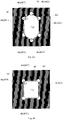
- the body shape of the black matrix opening 40 is obtained, based on the shape of the light emitting portion 20, by shifting various boundaries of the light emitting portion 20 outwards by a distance h in directions perpendicular to the boundaries (as shown by dotted arrows in Fig. 10A ), where specifically, h may range from 2 micrometers to 6 micrometers.
- a touch layer 8 is provided between the encapsulation layer 3 and the black matrix layer 4.
- the touch layer 8 includes a first insulation layer 81, a first metal layer 82, a second insulation layer 83, a second metal layer 84, and a third insulation layer 85 positioned at one side of the encapsulation layer 3 in sequence.
- the second metal layer 84 includes a plurality of first touch electrodes 841 extending in a first direction AB, and a plurality of second touch electrodes 842 extending in a second direction CD.
- the first touch electrodes 841 and the second touch electrodes 842 are insulated alternately.
- Each of the first touch electrodes 841 includes a plurality of first touch sub-electrode blocks 8411 connected to one another, and each of the second touch electrodes 842 includes a plurality of second touch sub-electrode blocks 8421 spaced from one another.
- the first metal layer 82 includes a plurality of bridging electrodes 820, and the second touch sub-electrode blocks 8421 in the same second direction CD are electrically connected through the bridging electrodes 820.
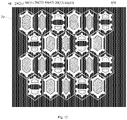
- the first touch sub-electrode blocks 8411, the second touch sub-electrode blocks 8421, and the bridging electrodes 820 are all provided with meshes (for example, hexagons enclosed by white lines in Fig. 12 ), orthographic projections of the meshes on the base substrate 1 cover orthographic projections of the light emitting portions 20 on the base substrate 1. That is, specifically, the first touch sub-electrode blocks 8411, the second touch sub-electrode blocks 8421, and the bridging electrodes 820 may be of structures with a plurality of meshes formed by metal lines 840.
- Fig. 12 shows corresponding relations between enlarged first touch sub-electrode blocks 8411, enlarged second touch sub-electrode blocks 8421, as well as enlarged bridging electrodes 820, and the light emitting portions 20, that is, Fig. 11B is an overall schematic diagram of the first touch sub-electrode blocks 8411, the second touch sub-electrode blocks 8421, and the bridging electrodes 820, and Fig.
- First touch sub-electrode blocks 8411 and second touch sub-electrode blocks 8421 in the same layer are spaced from one another, which may be specifically formed by breaking the metal lines 840 at corresponding positions.
- an orthographic projection, on the base substrate 1, of the region, except for the black matrix openings 40, of the black matrix layer 4 covers regions, except for the meshes, of the first touch sub-electrode blocks 8411 (that is, regions of the metal lines 840), regions, except for the meshes, of the second touch sub-electrode blocks 8421 (that is, regions of the metal lines 840), and regions, except for the meshes, of the bridging electrodes 820 (that is, regions of the metal lines 840).
- the protective layer 9 may be an optical adhesive layer, to protect the color resist portions 50 of the color filter layer 5 and the black matrix layer 4.
- An anode layer 61 may be further arranged between the pixel definition layer 7 and the base substrate 1.
- the anode layer 61 may include first-type anodes 611 corresponding to the first-type light emitting portions 21, second-type anodes 612 corresponding to the second-type light emitting portions 22, and third-type anodes 613 corresponding to the third-type light emitting portions 23.
- a cathode layer 62 may be further arranged between the light emitting layer 2 and the encapsulation layer 3. Specifically, the cathode layer 62 may be of a structure in an entire layer.
- a driving layer (not shown in the figure) may be further arranged between the anode layer 61 and the base substrate 1. Specifically, the driving layer may be provided with a pixel driving circuit for driving the display panel for display, and the pixel driving circuit may include a plurality of transistors and a plurality of capacitors.
- one side, away from the color filter layer 5, of the protective layer 9 is provided with a cover plate (not shown in the figure) or a covering filter layer (not shown in the figure).
- the cover plate may be a glass cover plate.
- a method for manufacturing the display panel provided in the embodiments of the present disclosure may specifically include the following operations.
- an anode layer, a pixel definition layer, a light emitting layer, a cathode layer, an encapsulation layer, and a touch layer are formed at one side of a base substrate in sequence.
- one side, away from the encapsulation layer, of the touch layer is coated with a light shielding thin membrane, that is, a basement membrane (BM).
- a light shielding thin membrane that is, a basement membrane (BM).
- the light shading thin membrane is exposed, developed, and cleaned, to obtain a black matrix layer with the black matrix openings.
- a patterned color filter layer is formed at one side, away from the touch layer, of the black matrix layer.
- an embodiment of the present disclosure further provides a display panel.
- the display panel includes a base substrate 1, a pixel definition layer 7, a light emitting layer 2, an encapsulation layer 3, a black matrix layer 4 and a color filter layer 5.
- the pixel definition layer 7 is arranged at one side of the base substrate 1 and provided with a plurality of pixel definition openings 70.
- the light emitting layer 2 is arranged at one side, away from the base substrate 1, of the pixel definition layer 7 and provided with a plurality of light emitting portions 20, and the light emitting portions 20 being positioned in the pixel definition openings 70.
- the encapsulation layer 3 is arranged at one side, away from the pixel definition layer 7, of the light emitting layer 2.
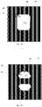
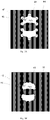
- the black matrix layer 4 is arranged at one side, away from the light emitting layer 2, of the encapsulation layer 3 and provided with black matrix openings 40 in regions corresponding to the light emitting portions 20, shapes of the black matrix openings 40 being circular (as shown in 13B) or elliptical (as shown in 13C), and orthographic projections, on the base substrate 1, of the black matrix openings 40 covering orthographic projections, on the base substrate 1, of the pixel definition openings 70.
- the color filter layer 5 is arranged at one side, away from the encapsulation layer 3, of the black matrix layer 4 and provided with color resist portions 50 in regions corresponding to the black matrix openings 40.
- centers of the black matrix openings 40 overlap centers of the light emitting portions 20.
- body shapes of the black matrix openings are circles or ellipses, and the orthographic projections, on the base substrate, of the black matrix openings cover the orthographic projections, on the base substrate, of the pixel definition openings.
- the body shapes of the black matrix openings in the embodiment of the present disclosure are circles or ellipses, thereby smoothing size mutations at the sharp corners and weakening a diffraction effect of reflected light generated after external ambient light passes through the display panel, to weaken a color separation phenomenon.
- an embodiment of the present disclosure further provides a display apparatus, including the display panel provided in the embodiments of the present disclosure; or the display panel further provided in the embodiments of the present disclosure.
- the embodiments of the present disclosure have the beneficial effects as follows: in the embodiments of the present disclosure, the body shapes of the black matrix openings are the polygons, and the black matrix openings are the cambered curves at least at the corners of the polygons, to realize the cambered transitional connections between the edges of the polygons.
- the black matrix openings in the embodiment of the present disclosure are provided with the cambered corners, thereby smoothing the size mutations at the sharp corners and weakening a diffraction effect of reflected light generated after external ambient light passes through the display panel, to weaken a color separation phenomenon.
Landscapes
- Electroluminescent Light Sources (AREA)
- Devices For Indicating Variable Information By Combining Individual Elements (AREA)
- Optical Filters (AREA)
- Physics & Mathematics (AREA)
- Optics & Photonics (AREA)
Abstract
Description
- The present application claims the priority of
Chinese Patent Application No. 202010552325.6, filed to the Chinese Patent Office on June 17, 2020 - The present disclosure relates to the field of displays, and in particular to a display panel and a display apparatus.
- With the multimedia developing, the display apparatuses are increasingly significant. In response to this, a variety of display apparatuses such as liquid crystal displays and organic light emitting displays have been put into use.
- Among various display apparatuses, the organic light emitting displays utilize the organic light emitting devices that generate light upon the recombination of electrons and holes, to display the images. The organic light emitting displays feature the short response time, high brightness, large visual angle, low power consumption, etc.
- The present disclosure provides a display panel, including: a base substrate; a light emitting layer, arranged at one side of the base substrate and provided with a plurality of light emitting portions; an encapsulation layer, arranged at one side, away from the base substrate, of the light emitting layer; a black matrix layer, arranged at one side, away from the light emitting layer, of the encapsulation layer and provided with a plurality of black matrix openings in regions corresponding to the plurality of light emitting portions, where body shapes of the black matrix openings are polygons and have cambered curves at least at corners of the polygons, to realize transitional connections among various edges of the polygons; and a color filter layer, arranged at one side, away from the encapsulation layer, of the black matrix layer and provided with a plurality of color resist portions in regions corresponding to the black matrix openings.
- In a possible implementation, the corners of the black matrix openings are circular arcs protruding towards one sides away from centers of the black matrix openings.
- In a possible implementation, the corners of the black matrix openings are the circular arcs with corner points as circle centers, and the corner points are intersection points between extension lines of adjacent edges.
- In a possible implementation, the corners of the black matrix openings are circular arcs dented towards one sides close to centers of the black matrix openings.
- In a possible implementation, the corners of the black matrix openings are the circular arcs with corner points as circle centers, and the corner points are intersection points between extension lines of adjacent edges.
- In a possible implementation, the body shapes of the black matrix openings are quadrilaterals, pentagons or hexagons; and radii of the circular arcs are one fifth to three fifths of lengths of the shortest edges of the black matrix openings.
- In a possible implementation, portions, except for the corners, of the edges of the black matrix openings are linear.
- In a possible implementation, portions, except for the corners, of the edges of the black matrix openings are arc segments protruding towards one sides away from the centers of the black matrix openings.
- In a possible implementation, portions, except for the corners, of the edges of the black matrix openings are arc segments dented towards the one sides close to the centers of the black matrix openings.
- In a possible implementation, the circular arcs at the corners are directly connected to the arc segments of the edges.
- In a possible implementation, orthographic projections, on the base substrate, of the black matrix openings cover orthographic projections, on the base substrate, of the light emitting portions.
- In a possible implementation, shapes of the light emitting portions are similar with the body shapes of the black matrix openings.
- In a possible implementation, the centers of the black matrix openings overlap centers of the light emitting portions.
- In a possible implementation, a pixel definition layer is arranged between the base substrate and the light emitting layer, the pixel definition layer is provided with a plurality of pixel definition openings, the light emitting portions are arranged in the pixel definition openings, and the shapes of the light emitting portions are consistent with shapes of the pixel definition openings.
- In a possible implementation, the shapes of the light emitting portions are expanded outwards by 2 micrometers-6 micrometers, to obtain the body shapes of the black matrix openings.
- In a possible implementation, a portion, except for the black matrix openings, of the black matrix layer is a black matrix body, and orthographic projections, on the base substrate, of the color resist portions cover a part of the back matrix body on peripheries of the black matrix openings.
- In a possible implementation, a touch layer is arranged between the encapsulation layer and the black matrix layer; the touch layer includes a first insulation layer, a first metal layer, a second insulation layer, a second metal layer, and a third insulation layer which are arranged at one side of the encapsulation layer in sequence; the second metal layer includes a plurality of first touch electrodes extending in a first direction and a plurality of second touch electrodes extending in a second direction, the first touch electrodes and the second touch electrodes are insulated alternately, each of the first touch electrodes includes a plurality of first touch sub-electrode blocks which are connected to one another, and each of the second touch electrodes includes a plurality of second touch sub-electrode blocks which are spaced from one another; and the first metal layer includes a plurality of bridging electrodes, and the second touch sub-electrode blocks in the same second direction being electrically connected through the bridging electrodes.
- In a possible implementation, the first touch sub-electrode blocks, the second touch sub-electrode blocks, and the bridging electrodes are provided with meshes, orthographic projections, on the base substrate, of the meshes cover the orthographic projections, on the base substrate, of the light emitting portions.
- In a possible implementation, an orthographic projection, on the base substrate, of the region, except for the black matrix openings, of the black matrix layer covers a region, except for the meshes, of the first touch sub-electrode blocks, a regions except for the meshes, of the second touch sub-electrode blocks, and a region, except for the meshes, of the bridging electrodes.
- In a possible implementation, one side, away from the black matrix layer, of the color filter layer is provided with a protective layer.
- In a possible implementation, one side, away from the color filter layer, of the protective layer is provided with a cover plate or a covering filter layer.
- An embodiment of the present disclosure further provides a display panel, including: a base substrate; a pixel definition layer, arranged at one side of the base substrate and provided with a plurality of pixel definition openings; a light emitting layer, arranged at one side, away from the base substrate, of the pixel definition layer and provided with a plurality of light emitting portions, and the light emitting portions are arranged in the pixel definition openings; an encapsulation layer, arranged at one side, away from the pixel definition layer, of the light emitting layer; a black matrix layer, arranged at one side, away from the light emitting layer, of the encapsulation layer and provided with black matrix openings in regions corresponding to the light emitting portions, where shapes of the black matrix openings are circles or ellipses, and orthographic projections, on the base substrate, of the black matrix openings cover orthographic projections, on the base substrate, of the pixel definition openings; and a color filter layer, arranged at one side, away from the encapsulation layer, of the black matrix layer and provided with color resist portions in regions corresponding to the black matrix openings.
- In a possible implementation, centers of the black matrix openings overlap centers of the light emitting portions.
- An embodiment of the present disclosure further provides a display apparatus, including: the display panel provided in the embodiments of the present disclosure; or the display panel further provided in the embodiments of the present disclosure.
-
-
Fig. 1A is a sectional structural schematic diagram of a display panel provided in an embodiment of the present disclosure. -
Fig. 1B is a top-view structural schematic diagram of a display panel provided in an embodiment of the present disclosure. -
Fig. 2A is a structural schematic diagram of a hexagonal black matrix opening with corners protruding outwards provided in an embodiment of the present disclosure. -
Fig. 2B is a structural schematic diagram of a quadrilateral black matrix opening with corners protruding outwards provided in an embodiment of the present disclosure. -
Fig. 2C is a structural schematic diagram of a pentagonal black matrix opening with corners protruding outwards provided in an embodiment of the present disclosure. -
Fig. 3A is a structural schematic diagram of a hexagonal black matrix opening with corners dented inwards provided in an embodiment of the present disclosure. -
Fig. 3B is a structural schematic diagram of a quadrilateral black matrix opening with corners dented inwards provided in an embodiment of the present disclosure. -
Fig. 3C is a structural schematic diagram of a pentagonal black matrix opening with corners dented inwards provided in an embodiment of the present disclosure. -
Fig. 4A is a structural schematic diagram of a hexagonal black matrix opening with corners protruding outwards and edges protruding outwards provided in an embodiment of the present disclosure. -
Fig. 4B is a structural schematic diagram of a hexagonal black matrix opening with corners dented inwards and edges protruding outwards provided in an embodiment of the present disclosure. -
Fig. 5A is a structural schematic diagram of a quadrilateral black matrix opening with corners protruding outwards and edges protruding outwards provided in an embodiment of the present disclosure. -
Fig. 5B is a structural schematic diagram of a quadrilateral black matrix opening with corners dented inwards and edges protruding outwards provided in an embodiment of the present disclosure. -
Fig. 6A is a structural schematic diagram of a pentagonal black matrix opening with corners protruding outwards and edges protruding outwards provided in an embodiment of the present disclosure. -
Fig. 6B is a structural schematic diagram of a pentagonal black matrix opening with corners dented inwards and edges protruding outwards provided in an embodiment of the present disclosure. -
Fig. 7A is a structural schematic diagram of a hexagonal black matrix opening with corners protruding outwards and edges dented inwards provided in an embodiment of the present disclosure. -
Fig. 7B is a structural schematic diagram of a hexagonal black matrix opening with corners dented inwards and edges dented inwards provided in an embodiment of the present disclosure. -
Fig. 8A is a structural schematic diagram of a quadrilateral black matrix opening with corners protruding outwards and edges dented inwards provided in an embodiment of the present disclosure. -
Fig. 8B is a structural schematic diagram of a quadrilateral black matrix opening with corners dented inwards and edges dented inwards provided in an embodiment of the present disclosure. -
Fig. 9A is a structural schematic diagram of a pentagonal black matrix opening with corners protruding outwards and edges dented inwards provided in an embodiment of the present disclosure. -
Fig. 9B is a structural schematic diagram of a pentagonal black matrix opening with corners dented inwards and edges dented inwards provided in an embodiment of the present disclosure. -
Fig. 10A is a schematic diagram of a hexagonal black matrix opening covering a light emitting portion provided in an embodiment of the present disclosure. -
Fig. 10B is a schematic diagram of a quadrilateral black matrix opening covering a light emitting portion provided in an embodiment of the present disclosure. -
Fig. 10C is a schematic diagram of a pentagonal black matrix opening covering a light emitting portion provided in an embodiment of the present disclosure. -
Fig. 11A is a specific structural schematic diagram of a display panel provided in an embodiment of the present disclosure. -
Fig. 11B is a top-view schematic diagram of a second metal layer provided in an embodiment of the present disclosure. -
Fig. 12 is a schematic diagram of a second metal layer with meshes provided in an embodiment of the present disclosure. -
Fig. 13A is a specific structural schematic diagram of another display panel provided in an embodiment of the present disclosure. -
Fig. 13B is a top-view structural schematic diagram of another display panel provided in the embodiment of the present disclosure. -
Fig. 13C is another top-view structural schematic diagram of another display panel provided in the embodiment of the present disclosure. - To make the objectives, technical solutions, and advantages in the embodiments of the present disclosure more clear, the technical solutions in the embodiments of the present disclosure will be clearly and completely described below in combination with the accompanying drawings in the embodiments of the present disclosure. It is obvious that the described embodiments are some, rather than all, embodiments of the present disclosure, not all of them. Based on the described embodiments of the present disclosure, all other embodiments obtained by a person of ordinary skill in the art without making inventive efforts fall within the scope of protection of the present disclosure.
- Unless defined otherwise, technical or scientific terms used in the present disclosure should be of ordinary meaning as understood by a person of ordinary skill in the art to which the present disclosure pertains. The words "first", "second", etc. used in the present disclosure do not denote any order, quantity, or importance, but are merely used for distinguishing between different components. The words "comprising", "including", etc. are intended to mean that an element or item in front of the word encompasses elements or items that present behind the word and equivalents thereof, but does not exclude other elements or items. The words "connection", "connected", etc. are not limited to the physical or mechanical connection, but may include the electrical connection, regardless of being direct or indirect. "Upper", "lower", "left", "right", etc. are merely used to indicate relative positional relations, which may also change accordingly when the absolute position of the described object changes.
- To keep the following description of the embodiments of the present disclosure clear and concise, the detailed descriptions of known functions and components are omitted from the present disclosure.
- As shown in
Figs. 1A, 1B , and2A ,Fig. 1A is a sectional schematic diagram ofFig. 1B at a dotted line EF, andFig. 2A is an enlarged schematic diagram of a black matrix opening inFig. 1B . An embodiment of the present disclosure provides a display panel, including abase substrate 1, alight emitting layer 2, anencapsulation layer 3, ablack matrix layer 4 and acolor filter layer 5. - The
base substrate 1 may be a glass substrate, a silicon substrate, or a flexible substrate. Thebase substrate 1 may be formed of, for example, a plastic material with excellent heat resistance and durability, such as polyimide (PI), polycarbonate (PC), polyethylene terephthalate (PET), polycarbonate, polyethylene, polyacrylate, polycarbonate, polyarylate, polyetherimide, polyethersulfone, polyethylene glycol terephthalate (PET), polyethylene (PE), polypropylene (PP), polysulfone (PSF), polymethylmethacrylate (PMMA), cellulose triacetate (TAC), cyclic olefin polymer (COP), cyclic olefin copolymer (COC), etc. - The
light emitting layer 2 is arranged at one side of thebase substrate 1 and provided with a plurality of light emittingportions 20. Specifically, thelight emitting portions 20 may include one or more first-typelight emitting portions 21, one or more second-typelight emitting portions 22, and one or more third-typelight emitting portions 23. Specifically, the first-typelight emitting portions 21 may be light emitting portions emitting blue light and made of organic light emitting materials emitting blue light; the second-typelight emitting portions 22 may be light emitting portions emitting red light and made of organic light emitting materials emitting red light; and the third-typelight emitting portions 23 may be light emitting portions emitting green light and made of organic light emitting materials emitting green light. - The
encapsulation layer 3 is arranged at one side, away from thebase substrate 1, of thelight emitting layer 2; and theencapsulation layer 3 may be a thin film encapsulation layer and may include a first inorganic encapsulation layer, an organic encapsulation layer, and a second inorganic encapsulation layer which are laminated in sequence. - The
black matrix layer 4 is arranged at one side, away from thelight emitting layer 2, of theencapsulation layer 3 and provided withblack matrix openings 40 in regions corresponding to thelight emitting portions 20. A body shape of the black matrix opening 40 (as shown by a dotted hexagonal frame inFig. 2A ) is a polygon and has cambered curves at least atcorners 45 of the polygon, to realize transitional connections betweenvarious edges 46 of the polygon. Specifically, a portion, except for theblack matrix openings 40, of theblack matrix layer 4 is a black matrix body, that is, a region except for theblack matrix openings 40 may be theblack matrix body 44. It may be understood that a body shape of ablack matrix opening 40 may be specifically interpreted as a main outline of theblack matrix opening 40, andspecific edges 46 may be non-linear line segments, but an overall shape of theback matrix opening 40 is still a polygon. For example, a body shape of theblack matrix opening 40 may be a rectangle, but four edges of the rectangle may be cambered. In some embodiments, each of the edges of theblack matrix opening 40 may also be linear. Theblack matrix openings 40 correspond to thelight emitting portions 20, which may be understood that orthographic projections, on thebase substrate 1, of theblack matrix openings 40 cover orthographic projections, on thebase substrate 1, of thelight emitting portions 20, and theblack matrix layer 4 is correspondingly provided with an opening at a position of each of thelight emitting portions 20, to form theblack matrix openings 40 corresponding one-to-one to thelight emitting portions 20, so that the light emitted by thelight emitting portions 20 is emitted through theblack matrix openings 40. As shown inFigs. 1A and 1B , theblack matrix openings 40 may include first-typeblack matrix openings 41 corresponding to the first-typelight emitting portions 21, second-typeblack matrix openings 42 corresponding to the second-typelight emitting portions 22, and third-typeblack matrix openings 43 corresponding to the third-typelight emitting portions 23. Body shapes of the first-typeblack matrix openings 41 may be consistent with shapes of the first-typelight emitting portions 21, and may be, for example, all hexagons; body shapes of the second-typeblack matrix openings 42 may be consistent with shapes of the second-typelight emitting portions 22; and body shapes of the third-typeblack matrix openings 43 may be consistent with shapes of the third-typelight emitting portions 23. - The
color filter layer 5 is arranged at one side, away from theencapsulation layer 3, of theblack matrix layer 4 and provided with color resistportions 50 in regions corresponding to theblack matrix openings 40. Specifically, since the color resistportions 50 are arranged at positions corresponding to theblack matrix openings 40 of theblack matrix layer 4, and theblack matrix openings 40 correspond to thelight emitting portions 20, positions of the color resistportions 50 also correspond to positions of thelight emitting portions 20. Specifically, the color resistportions 50 may include first-type color resistportions 51 corresponding to the first-typelight emitting portions 21, second-type color resistportions 52 corresponding to the second-typelight emitting portions 22, and third-type color resistportions 53 corresponding to the third-typelight emitting portions 23. When the first-typelight emitting portions 21 are the light emitting portions emitting the blue light, the first-type color resistportions 51 may be blue color resist portions that transmit the blue light and block transmission of other light colors; when the second-typelight emitting portions 22 are the light emitting portions that emit the red light, the second-type color resistportions 52 may be red color resist portions that transmit the red light and block transmission of other light colors; and when the third-typelight emitting portions 23 are the light emitting portions that emit the green light, the third-type color resistportions 53 may be green color resist portions that transmit the green light and block transmission of other light colors. - In embodiments of the present disclosure, the body shapes of the
black matrix openings 40 are the polygons, and theblack matrix openings 40 are the cambered curves at least at thecorners 45 of the polygons, to realize cambered transitional connections among theedges 46 of the polygons. Compared with a conventional display panel in which black matrix openings close up sharply at corners, the cambered corners in the embodiments of the present disclosure are provided, thereby smoothing size mutations at sharp corners and weakening a diffraction effect of reflected light generated after external ambient light passes through the display panel, to weaken a color separation phenomenon. - It may be understood that the display panel in the embodiments of the present disclosure may include no circular polarizer. Through the
color filter layer 5 and theblack matrix layer 4 as provided in the embodiments of the present disclosure, at a position where display is required, that is, the positions of thelight emitting portions 20, the light emitted from thelight emitting portions 20 is emitted through theblack matrix openings 40, without affecting the display. Theblack matrix body 44 may block a position except for thelight emitting portions 20, so that the external ambient light fails to enter, and the circular polarizer may prevent the external light from being reflected. - It should be noted that color separation refers to a phenomenon that reflected light shows color (red, green, and blue) separation under irradiation of ambient light (for example, a point light source and a line light source) in a screen rest state. For the display panel with the color filter layer and the black matrix layer instead of the circular polarizer, as shown in
Fig. 1A , under the ambient light, light rays pass through thecolor filter layer 5 and become monochromatic light, the monochromatic light enters a metal film layer (for example, an anode layer and/or a cathode layer, not shown inFig. 1A ) at a bottom of the display panel and is reflected by the metal film layer, and the monochromatic reflected light passes through theblack matrix openings 40 and is emitted out. Since the small black matrix openings 40 (for example, when the black matrix openings are in the order of λ∗102, where λ is a wavelength of the reflected light), when theblack matrix openings 40 are rectangular or hexagonal with the sharp corners, it is inevitable for a screen to generate the diffraction effect of the monochromatic (R, G, B) light under the ambient light (specifically, the point light source). These diffraction effects further increase the color separation. - During specific implementation, as shown in
Fig. 1A , apixel definition layer 7 is arranged between thebase substrate 1 and thelight emitting layer 2. Thepixel definition layer 7 is provided with a plurality ofpixel definition openings 70, thelight emitting portions 20 are arranged in thepixel definition openings 70, and shapes of thelight emitting portions 20 are consistent with shapes of thepixel definition openings 70. It may be understood that in a process for manufacturing the display panel, thepixel definition layer 7 with thepixel definition openings 70 is formed first, and then thelight emitting portions 20 are formed in thepixel definition openings 70, so that the shapes of thelight emitting portions 20 are consistent with the shapes of thepixel definition openings 70. It may be understood that specifically, thelight emitting portions 20 may be positions occupied by light emitting regions of the display panel during display, that is, during specific implementation, for each sub-pixel, a light emitting material formed at a position of the pixel definition opening may be larger than a region occupied by the pixel definition opening. However, the light emitting regions depend on an area of a light emitting material at a power-on position, that is, thelight emitting portions 20 depend on a size of regions, making contact with anodes, of the light emitting materials. - During specific implementation, as shown in
Figs. 2A-2C , ablack matrix opening 40 has circular arcs at thecorners 45 protruding towards one sides away from a center O of theblack matrix opening 40. Specifically, theblack matrix opening 40 has the circular arcs, where the circular arcs are arranged at thecorners 45, and protruding towards one sides away from the center O of theblack matrix opening 40 by taking corner points O' as circle centers, and the corner points O' are intersection points between extension lines of adjacent edges 46. - For example, as shown in
Fig. 2A , a body shape of ablack matrix opening 40 is a hexagon with sixedges 46, every twoadjacent edges 46 of the sixedges 46 intersect each other to form sixcorners 45, each of thecorners 45 has a corner point O', and non-closed circular arcs (that is, circular arcs protruding outwards) may be arranged at thecorners 45, where the non-closed circular arcs take the corner points O' as circle centers and protrude towards one sides away from the center O of theblack matrix opening 40, to realize cambered transitions betweenadjacent edges 46 at thecorners 45. - Alternatively, as shown in
Fig. 2B , a body shape of ablack matrix opening 40 is a quadrilateral with fouredges 46, every twoadjacent edges 46 of the four edges intersect each other to form fourcorners 45, each of thecorners 45 has a corner point O', and non-closed circular arcs (that is, circular arcs protruding outwards) may be arranged at thecorners 45, where the non-closed circular arcs take the corner points O' as circle centers and protrude towards one sides away from the center O of theblack matrix opening 40, to realize cambered transitions betweenadjacent edges 46 at thecorners 45. - Alternatively, as shown in
Fig. 2C , a body shape of ablack matrix opening 40 is a pentagon with fiveedges 46, every twoadjacent edges 46 of the five edges intersect each other to form fivecorners 45, each of thecorners 45 has a corner point O', and non-closed circular arcs (that is, circular arcs protruding outwards) may be arranged at thecorners 45, where the non-closed circular arcs take the corner points O' as circle centers and protrude towards one sides away from the center O of theblack matrix opening 40, to realize cambered transitions betweenadjacent edges 46 at thecorners 45. - During specific implementation, a
black matrix opening 40 has circular arcs at thecorners 45 dented towards one sides close to a center O of theblack matrix opening 40. Specifically, theblack matrix opening 40 has the circular arcs, where the circular arcs are arranged at thecorners 45, and are dented towards one sides close to the center O of theblack matrix opening 40 by taking the corner points O' as circle centers, and the corner points O' are intersection points between extension lines of adjacent edges 46. - For example, as shown in
Fig. 3A , a body shape of ablack matrix opening 40 is a hexagon with sixedges 46, every twoadjacent edges 46 of the sixedges 46 intersect each other to form sixcorners 45, each of thecorners 46 has a corner point O', and non-closed circular arcs (that is, circular arcs dented inwards) may be arranged at thecorners 45, where the non-closed circular arcs take the corner points O' as circle centers and are dented towards one sides close to the center O of theblack matrix opening 40, to realize cambered transitions betweenadjacent edges 46 at thecorners 45. - Alternatively, as shown in
Fig. 3B , a body shape of ablack matrix opening 40 is a quadrilateral with fouredges 46, every twoadjacent edges 46 of the four edges intersect each other to form fourcorners 45, each of thecorners 45 has a corner point O', and non-closed circular arcs (that is, circular arcs dented inwards) may be arranged at thecorners 45, where the non-closed circular arcs take the corner points O' as circle centers and are dented towards one sides close to the center O of theblack matrix opening 40, to realize cambered transitions betweenadjacent edges 46 at thecorners 45. - Alternatively, as shown in
Fig. 3C , a body shape of ablack matrix opening 40 is a pentagon with fiveedges 46, every twoadjacent edges 46 of the five edges intersect each other to form fivecorners 45, each of thecorners 45 has a corner point O', and non-closed circular arcs (that is, circular arcs dented inwards) may be arranged at thecorners 45, where the non-closed circular arcs take the corner points O' as circle centers and are dented towards one sides close to the center O of theblack matrix opening 40, to realize cambered transitions betweenadjacent edges 46 at thecorners 45. - During specific implementation, a body shape of a
black matrix opening 40 is a quadrilateral, a pentagon, or a hexagon; and a radius of a circular arc is one fifth to one half of a length of thesmallest edge 46 of theblack matrix opening 40. - In some embodiments, as shown in
Fig. 2A , a body shape of ablack matrix opening 40 is the hexagon, and the hexagon has two first-type edges 461 arranged opposite and parallel to each other, second-type edges 462 connected to first ends of the two first-type edges 461 respectively, and third-type edges 463 connected to second ends of the two first-type edges 461 respectively. Extension lengths of the first-type edges 461 are greater than extension lengths of the second-type edges 462 and extension lengths of the third-type edges 463, and the extension lengths of the second-type edges 462 are the same as the extension lengths of the third-type edges 462. Therefore, in the hexagon, radii of the circular arcs at thecorners 45 may be one fifth to one half of lengths of the second-type edges 462. - In some embodiments, as shown in
Fig. 2B , a body shape of ablack matrix opening 40 is the quadrilateral, and the quadrilateral has two fourth-type edges 464 arranged opposite and parallel to each other, and fifth-type edges 465 connecting corresponding ends of the two fourth-type edges 464 respectively. Extension lengths of the fourth-type edges 464 are greater than extension lengths of the fifth-type edges 465. Therefore, in the quadrilateral, radii of the circular arcs at thecorners 45 may be one fifth to one half of lengths of the fifth-type edges 465. - In some embodiments, as shown in
Fig. 2C , a body shape of ablack matrix opening 40 is the pentagon, and the pentagon has two sixth-type edges 466 arranged opposite and parallel to each other, seventh-type edges 467 connected to first ends of the two sixth-type edges 466 respectively, and an eighth-type edge 468 connecting two second ends of the two sixth-type edges 466, respectively. Extension lengths of the sixth-type edges 466 are smaller than extension lengths of the seventh-type edges 467, and lengths of the seventh-type edges 467 are smaller than a length of the eighth-type edge 468. Therefore, in the pentagon, radii of the circular arcs at thecorners 45 may be one fifth to one half of lengths of the sixth-type edges 466. In the embodiments of the present disclosure, the radii of the circular arcs are one fifth to three fifths of lengths of the shortest edges of the black matrix openings. - During specific implementation, portions, except for the
corners 45, of theedges 46 of theblack matrix openings 40 are linear. For example, as shown inFig. 2A , the body shape of theblack matrix opening 40 is the hexagon with circular arcs protruding outwards at thecorners 45 and thelinear edges 46; as shown inFig. 3A , the body shape of theblack matrix opening 40 is the hexagon with circular arcs dented inwards at thecorners 45 and thelinear edges 46; as shown inFig. 2B , the body shape of theblack matrix opening 40 is the quadrilateral with circular arcs protruding outwards at thecorners 45 and thelinear edges 46; as shown inFig. 3B , the body shape of theblack matrix opening 40 is the quadrilateral with circular arcs dented inwards at thecorners 45 and thelinear edges 46; as shown inFig. 2C , the body shape of theblack matrix opening 40 is the pentagon with circular arcs protruding outwards at thecorners 45 and thelinear edges 46; and as shown inFig. 3C , the body shape of theblack matrix opening 40 is the pentagon with circular arcs dented inwards at thecorners 45 and the linear edges 46. - During specific implementation, portions, except for the
corners 45, of theedges 46 of theblack matrix openings 40 are arc segments protruding towards one sides away from the centers O of theblack matrix openings 40, that is, theedges 46 are arc segments protruding outwards. For example, as shown inFig. 4A , a body shape of ablack matrix opening 40 is the hexagon with circular arcs protruding outwards atcorners 45 and arc segments protruding outwards asedges 46; and as shown inFig. 4B , a body shape of ablack matrix opening 40 is the hexagon with circular arcs dented inwards atcorners 45 and arc segments protruding outwards as edges 46. For example, as shown inFig. 5A , a body shape of ablack matrix opening 40 is the quadrilateral with circular arcs protruding outwards atcorners 45 and arc segments protruding outwards asedges 46; and as shown inFig. 5B , a body shape of ablack matrix opening 40 is the quadrilateral with circular arcs dented inwards atcorners 45 and arc segments protruding outwards as edges 46. For example, as shown inFig. 6A , a body shape of ablack matrix openings 40 is the pentagon with circular arcs protruding outwards atcorners 45 and arc segments protruding outwards asedges 46; and as shown inFig. 6B , a body shape of ablack matrix opening 40 is the pentagon with circular arcs dented inwards atcorners 45 and arc segments protruding outwards as edges 46. - During specific implementation, portions, except for the
corners 45, of theedges 46 of theblack matrix openings 40 are arc segments dented towards one sides close to the centers O of theblack matrix openings 40, that is, theedges 46 are arc segments dented inwards. For example, as shown inFig. 7A , a body shape of ablack matrix openings 40 is the hexagon with circular arcs protruding outwards atcorners 45 and arc segments dented inwards asedges 46; and as shown inFig. 7B , a body shape of ablack matrix opening 40 is the hexagons with circular arcs dented inwards atcorners 45 and arc segments dented inwards as edges 46. For example, as shown inFig. 8A , a body shape of ablack matrix opening 40 is the quadrilateral with circular arcs protruding outwards atcorners 45 and arc segments dented inwards asedges 46; and as shown inFig. 8B , a body shape of ablack matrix opening 40 is the quadrilateral with circular arcs dented inwards atcorners 45 and arc segments dented inwards as edges 46. For example, as shown inFig. 9A , a body shape of ablack matrix opening 40 is the pentagon with circular arcs protruding outwards atcorners 45 and arc segments dented inwards asedges 46; and as shown inFig. 9B , a body shape of ablack matrix opening 40 is the pentagon with circular arcs dented inwards atcorners 45 and arc segments dented inwards as edges 46. - During specific implementation, the circular arcs at the
corners 45 are directly connected to the arc segments of theedges 46. For example, as shown in 7B, the body shape of theblack matrix opening 40 is the hexagons with circular arcs dented inwards atcorners 45 and arc segments dented inwards asedges 46, and the arc segments at theedges 46 are directly connected to the circular arcs at thecorners 45. For example, as shown in 8B, the body shape of theblack matrix opening 40 is the quadrilateral with circular arcs dented inwards atcorners 45 and arc segments dented inwards asedges 46, and the arc segments at theedges 46 are directly connected to the circular arcs at thecorners 45. - It should be noted that
Fig. 1B is only a schematic illustration showing that the body shapes of all the black matrix openings are hexagons, thecorners 45 are all the arcs protruding outwards, and theedges 46 are all linear. The present disclosure is not limited thereto. During specific implementation, the body shapes of theblack matrix openings 40 at different positions may be different, and shapes of thecorners 45 and shapes of the edges of theblack matrix openings 40 at different positions may be any combination ofFigs. 2A-2C ,Figs. 3A-3C ,Figs. 4A-4B ,Figs. 5A-5B ,Figs. 6A-6B ,Figs. 7A-7B ,Figs. 8A-8B , andFigs. 9A-9B . In addition, in the embodiments of the present disclosure, the circular arcs at the corners may be other circular arcs not with the corner points as the circle centers, that is, the circle centers may not be located at the corner points, and the present disclosure is not limited thereto. - During specific implementation, as shown in
Fig. 1B , orthographic projections of theblack matrix openings 40 on thebase substrate 1 cover orthographic projections of thelight emitting portions 20 on thebase substrate 1. That is, theblack matrix openings 40 are required to be larger than thelight emitting portions 20, thereby preventing theblack matrix body 22 from affecting light emitting conditions of thelight emitting portions 20. It may be understood that in the present disclosure, the orthographic projections of theblack matrix openings 40 on thebase substrate 1 cover the orthographic projections of thelight emitting portions 20 on thebase substrate 1, with thecorners 45 of theblack matrix openings 40 designed as the circular arcs protruding outwards or dented inwards, and theedges 46 designed as the arc segments protruding outwards or dented inwards, that is, after theblack matrix openings 40 in the embodiments of the present disclosure are improved, the orthographic projections of the black matrix openings on thebase substrate 1, still cover the orthographic projections of thelight emitting portions 20 on thebase substrate 1. - During specific implementation, the shapes of the
light emitting portions 20 are similar with the body shapes of theblack matrix openings 40. For example, as shown inFig. 10A , a body shape of ablack matrix opening 40 is the hexagon, and a shape of a correspondinglight emitting portion 20 is also the hexagon. For example, as shown inFig. 10B , a body shape of a black matrix opening is the quadrilateral, and a shape of a correspondinglight emitting portion 20 is also the quadrilateral. For example, as shown inFig. 10C , a body shape of ablack matrix opening 40 is the pentagon, and a shape of a correspondinglight emitting portion 20 is also the pentagon. - During specific implementation, centers of the
black matrix openings 40 overlap centers of thelight emitting portions 20. Certainly, it may be understood that during actual manufacturing, due to limitation of the process accuracy, it is difficult to make the centers of theblack matrix openings 40 completely and accurately overlap the centers of thelight emitting portions 20. Therefore, in the embodiments of the present disclosure, overlapping between the centers of theblack matrix openings 40 and the centers of thelight emitting portions 20 may be interpreted as approximate overlapping therebetween. - During specific implementation, the shapes of the
light emitting portions 20 are expanded outwards by 2 micrometers-6 micrometers to obtain the body shapes of theblack matrix openings 40. For example, as shown inFig. 10A , the body shape of theblack matrix opening 40 is the hexagons, and the shape of the correspondinglight emitting portion 20 is also the hexagon, such that the black matrix opening and the light emitting portion are similar in shape and overlap in centers. The body shape of theblack matrix opening 40 is obtained, based on the shape of thelight emitting portion 20, by shifting various boundaries of thelight emitting portion 20 outwards by a distance h in directions perpendicular to the boundaries (as shown by dotted arrows inFig. 10A ), where specifically, h may range from 2 micrometers to 6 micrometers. - During specific implementation, as shown in
Figs. 11A and11B , atouch layer 8 is provided between theencapsulation layer 3 and theblack matrix layer 4. Thetouch layer 8 includes afirst insulation layer 81, afirst metal layer 82, asecond insulation layer 83, asecond metal layer 84, and athird insulation layer 85 positioned at one side of theencapsulation layer 3 in sequence. Thesecond metal layer 84 includes a plurality offirst touch electrodes 841 extending in a first direction AB, and a plurality ofsecond touch electrodes 842 extending in a second direction CD. Thefirst touch electrodes 841 and thesecond touch electrodes 842 are insulated alternately. Each of thefirst touch electrodes 841 includes a plurality of first touch sub-electrode blocks 8411 connected to one another, and each of thesecond touch electrodes 842 includes a plurality of second touch sub-electrode blocks 8421 spaced from one another. Thefirst metal layer 82 includes a plurality of bridgingelectrodes 820, and the second touch sub-electrode blocks 8421 in the same second direction CD are electrically connected through the bridgingelectrodes 820. - During specific implementation, as shown in
Fig. 12 , the first touch sub-electrode blocks 8411, the second touch sub-electrode blocks 8421, and the bridgingelectrodes 820 are all provided with meshes (for example, hexagons enclosed by white lines inFig. 12 ), orthographic projections of the meshes on thebase substrate 1 cover orthographic projections of thelight emitting portions 20 on thebase substrate 1. That is, specifically, the first touch sub-electrode blocks 8411, the second touch sub-electrode blocks 8421, and the bridgingelectrodes 820 may be of structures with a plurality of meshes formed bymetal lines 840. It may be understood that since higher pixel accuracy is required relative to touch accuracy, areas of the first touch sub-electrodes blocks 8411 and the second touch sub-electrode blocks 8421 are far larger than areas of thelight emitting portions 20. Therefore,Fig. 12 shows corresponding relations between enlarged first touch sub-electrode blocks 8411, enlarged second touch sub-electrode blocks 8421, as well asenlarged bridging electrodes 820, and thelight emitting portions 20, that is,Fig. 11B is an overall schematic diagram of the first touch sub-electrode blocks 8411, the second touch sub-electrode blocks 8421, and the bridgingelectrodes 820, andFig. 12 shows the corresponding relations between the enlarged first touch sub-electrode blocks, the enlarged second touch sub-electrode blocks, as well as the enlarged bridging electrodes, and thelight emitting portions 20. First touchsub-electrode blocks 8411 and second touch sub-electrode blocks 8421 in the same layer are spaced from one another, which may be specifically formed by breaking themetal lines 840 at corresponding positions. - During specific implementation, as shown in
Fig. 12 , an orthographic projection, on thebase substrate 1, of the region, except for theblack matrix openings 40, of the black matrix layer 4 (that is, the black matrix body 44) covers regions, except for the meshes, of the first touch sub-electrode blocks 8411 (that is, regions of the metal lines 840), regions, except for the meshes, of the second touch sub-electrode blocks 8421 (that is, regions of the metal lines 840), and regions, except for the meshes, of the bridging electrodes 820 (that is, regions of the metal lines 840). - During specific implementation, as shown in
Fig. 11A , one side, away from theblack matrix layer 4, of thecolor filter layer 5 is provided with aprotective layer 9. Specifically, theprotective layer 9 may be an optical adhesive layer, to protect the color resistportions 50 of thecolor filter layer 5 and theblack matrix layer 4. Ananode layer 61 may be further arranged between thepixel definition layer 7 and thebase substrate 1. Specifically, theanode layer 61 may include first-type anodes 611 corresponding to the first-typelight emitting portions 21, second-type anodes 612 corresponding to the second-typelight emitting portions 22, and third-type anodes 613 corresponding to the third-typelight emitting portions 23. Acathode layer 62 may be further arranged between the light emittinglayer 2 and theencapsulation layer 3. Specifically, thecathode layer 62 may be of a structure in an entire layer. A driving layer (not shown in the figure) may be further arranged between theanode layer 61 and thebase substrate 1. Specifically, the driving layer may be provided with a pixel driving circuit for driving the display panel for display, and the pixel driving circuit may include a plurality of transistors and a plurality of capacitors. - During specific implementation, one side, away from the
color filter layer 5, of theprotective layer 9 is provided with a cover plate (not shown in the figure) or a covering filter layer (not shown in the figure). Specifically, the cover plate may be a glass cover plate. - A method for manufacturing the display panel provided in the embodiments of the present disclosure may specifically include the following operations.
-
Operation 1, a mask plate corresponding to patterns of black matrix openings in the embodiments of the present disclosure is provided. -
Operation 2, an anode layer, a pixel definition layer, a light emitting layer, a cathode layer, an encapsulation layer, and a touch layer are formed at one side of a base substrate in sequence. -
Operation 3, one side, away from the encapsulation layer, of the touch layer is coated with a light shielding thin membrane, that is, a basement membrane (BM). -
Operation 4, the light shading thin membrane is exposed, developed, and cleaned, to obtain a black matrix layer with the black matrix openings. -
Operation 5, a patterned color filter layer is formed at one side, away from the touch layer, of the black matrix layer. - Based on the same inventive concept, an embodiment of the present disclosure further provides a display panel. With reference to
Figs. 13A-13C , the display panel includes abase substrate 1, apixel definition layer 7, alight emitting layer 2, anencapsulation layer 3, ablack matrix layer 4 and acolor filter layer 5. - The
pixel definition layer 7 is arranged at one side of thebase substrate 1 and provided with a plurality ofpixel definition openings 70. - The
light emitting layer 2 is arranged at one side, away from thebase substrate 1, of thepixel definition layer 7 and provided with a plurality of light emittingportions 20, and thelight emitting portions 20 being positioned in thepixel definition openings 70. - The
encapsulation layer 3 is arranged at one side, away from thepixel definition layer 7, of thelight emitting layer 2. - The
black matrix layer 4 is arranged at one side, away from thelight emitting layer 2, of theencapsulation layer 3 and provided withblack matrix openings 40 in regions corresponding to thelight emitting portions 20, shapes of theblack matrix openings 40 being circular (as shown in 13B) or elliptical (as shown in 13C), and orthographic projections, on thebase substrate 1, of theblack matrix openings 40 covering orthographic projections, on thebase substrate 1, of thepixel definition openings 70. - The
color filter layer 5 is arranged at one side, away from theencapsulation layer 3, of theblack matrix layer 4 and provided with color resistportions 50 in regions corresponding to theblack matrix openings 40. - During specific implementation, as shown in
Figs. 13B and13C , centers of theblack matrix openings 40 overlap centers of thelight emitting portions 20. - In an embodiment of the present disclosure, body shapes of the black matrix openings are circles or ellipses, and the orthographic projections, on the base substrate, of the black matrix openings cover the orthographic projections, on the base substrate, of the pixel definition openings. Compared with a conventional display panel in which black matrix openings close up sharply at corners, the body shapes of the black matrix openings in the embodiment of the present disclosure are circles or ellipses, thereby smoothing size mutations at the sharp corners and weakening a diffraction effect of reflected light generated after external ambient light passes through the display panel, to weaken a color separation phenomenon.
- Based on the same inventive concept, an embodiment of the present disclosure further provides a display apparatus, including the display panel provided in the embodiments of the present disclosure; or the display panel further provided in the embodiments of the present disclosure.
- The embodiments of the present disclosure have the beneficial effects as follows: in the embodiments of the present disclosure, the body shapes of the black matrix openings are the polygons, and the black matrix openings are the cambered curves at least at the corners of the polygons, to realize the cambered transitional connections between the edges of the polygons. Compared with the conventional display panel in which the black matrix openings close up sharply at the corners, the black matrix openings in the embodiment of the present disclosure are provided with the cambered corners, thereby smoothing the size mutations at the sharp corners and weakening a diffraction effect of reflected light generated after external ambient light passes through the display panel, to weaken a color separation phenomenon.
- Obviously, a person skilled in the art may make various amendments and variations to the present disclosure without departing from the spirit and scope of the present disclosure. In this way, it is intended that the present disclosure also includes these amendments and variations if the amendments and variations to the present disclosure fall within the scope of claims of the present disclosure and the equivalents thereof.
Claims (24)
- A display panel, comprising:a base substrate;a light emitting layer, arranged at one side of the base substrate and provided with a plurality of light emitting portions;an encapsulation layer, arranged at one side, away from the base substrate, of the light emitting layer;a black matrix layer, arranged at one side, away from the light emitting layer, of the encapsulation layer and provided with a plurality of black matrix openings in regions corresponding to the plurality of light emitting portions, wherein body shapes of the black matrix openings are polygons and have cambered curves at least at corners of the polygons, to realize transitional connections among edges of the polygons; anda color filter layer, arranged at one side, away from the encapsulation layer, of the black matrix layer and provided with a plurality of color resist portions in regions corresponding to the black matrix openings.
- The display panel according to claim 1, wherein the corners of the black matrix openings are circular arcs protruding towards one sides away from centers of the black matrix openings.
- The display panel according to claim 2, wherein the corners of the black matrix openings are the circular arcs with corner points as circle centers, and the corner points are intersection points between extension lines of adjacent edges.
- The display panel according to claim 1, wherein the corners of the black matrix openings are circular arcs dented towards one sides close to centers of the black matrix openings.
- The display panel according to claim 4, wherein the corners of the black matrix openings are the circular arcs with corner points as circle centers, and the corner points are intersection points between extension lines of adjacent edges.
- The display panel according to claim 3 or 5, wherein the body shapes of the black matrix openings are quadrilaterals, pentagons, or hexagons; and
radii of the circular arcs are one fifth to three fifths of lengths of shortest edges of the black matrix openings. - The display panel according to claim 2 or 4, wherein portions, except for the corners, of the edges of the black matrix openings are linear.
- The display panel according to claim 2 or 4, wherein portions, except for the corners, of the edges of the black matrix openings are arc segments protruding towards the one sides away from the centers of the black matrix openings.
- The display panel according to claim 2 or 4, wherein portions, except for the corners, of the edges of the black matrix openings are arc segments dented towards the one sides close to the centers of the black matrix openings.
- The display panel according to claim 9, wherein the circular arcs at the corners are directly connected to the arc segments of the edges.
- The display panel according to claim 1, wherein orthographic projections, on the base substrate, of the black matrix openings cover orthographic projections, on the base substrate, of the light emitting portions.
- The display panel according to claim 10, wherein shapes of the light emitting portions are similar with the body shapes of the black matrix openings.
- The display panel according to claim 12, wherein the centers of the black matrix openings overlap centers of the light emitting portions.
- The display panel according to claim 12, wherein a pixel definition layer is arranged between the base substrate and the light emitting layer, the pixel definition layer is provided with a plurality of pixel definition openings, the light emitting portions are arranged in the pixel definition openings, and the shapes of the light emitting portions are consistent with shapes of the pixel definition openings.
- The display panel according to claim 12, wherein the shapes of the light emitting portions are expanded outwards by 2 micrometers-6 micrometers, to obtain the body shapes of the black matrix openings.
- The display panel according to claim 1, wherein a portion, except for the black matrix openings, of the black matrix layer is a black matrix body, and orthographic projections, on the base substrate, of the color resist portions cover a part of the black matrix body on peripheries of the black matrix openings.
- The display panel according to claim 1, wherein a touch layer is arranged between the encapsulation layer and the black matrix layer;the touch layer comprises a first insulation layer, a first metal layer, a second insulation layer, a second metal layer, and a third insulation layer which are arranged at one side of the encapsulation layer in sequence;the second metal layer comprises a plurality of first touch electrodes extending in a first direction and a plurality of second touch electrodes extending in a second direction, the first touch electrodes and the second touch electrodes are insulated alternately, each of the first touch electrodes comprises a plurality of first touch sub-electrode blocks which are connected to one another, and each of the second touch electrodes comprises a plurality of second touch sub-electrode blocks which are spaced from one another; andthe first metal layer comprises a plurality of bridging electrodes, and the second touch sub-electrode blocks in the same second direction are electrically connected through the bridging electrodes.
- The display panel according to claim 17, wherein the first touch sub-electrode blocks, the second touch sub-electrode blocks, and the bridging electrodes are provided with meshes, orthographic projections, on the base substrate, of the meshes cover the orthographic projections, on the base substrate, of the light emitting portions.
- The display panel according to claim 18, wherein an orthographic projection, on the base substrate, of a region, except for the black matrix openings, of the black matrix layer covers a region, except for the meshes, of the first touch sub-electrode blocks, a region, except for the meshes, of the second touch sub-electrode blocks, and a region, except for the meshes, of the bridging electrodes.
- The display panel according to claim 17, wherein one side, away from the black matrix layer, of the color filter layer is provided with a protective layer.
- The display panel according to claim 20, wherein one side, away from the color filter layer, of the protective layer is provided with a cover plate or a covering filter layer.
- A display panel, comprising:a base substrate;a pixel definition layer, arranged at one side of the base substrate and provided with a plurality of pixel definition openings;a light emitting layer, arranged at one side, away from the base substrate, of the pixel definition layer and provided with a plurality of light emitting portions arranged in the pixel definition openings;an encapsulation layer, arranged at one side, away from the pixel definition layer, of the light emitting layer;a black matrix layer, arranged at one side, away from the light emitting layer, of the encapsulation layer and provided with black matrix openings in regions corresponding to the light emitting portions, wherein shapes of the black matrix openings are circles or ellipses, and orthographic projections, on the base substrate, of the black matrix openings cover orthographic projections, on the base substrate, of the pixel definition openings; anda color filter layer, arranged at one side, away from the encapsulation layer, of the black matrix layer and provided with color resist portions in regions corresponding to the black matrix openings.
- The display panel according to claim 22, wherein centers of the black matrix openings overlap centers of the light emitting portions.
- A display apparatus, comprising the display panel according to any one of claims 1-21 or the display panel according to claim 22 or 23.
Applications Claiming Priority (2)
| Application Number | Priority Date | Filing Date | Title |
|---|---|---|---|
| CN202010552325.6A CN113809258B (en) | 2020-06-17 | 2020-06-17 | Display panel and display device |
| PCT/CN2021/093443 WO2021254044A1 (en) | 2020-06-17 | 2021-05-12 | Display panel and display apparatus |
Publications (2)
| Publication Number | Publication Date |
|---|---|
| EP4036999A1 true EP4036999A1 (en) | 2022-08-03 |
| EP4036999A4 EP4036999A4 (en) | 2023-01-11 |
Family
ID=78943419
Family Applications (1)
| Application Number | Title | Priority Date | Filing Date |
|---|---|---|---|
| EP21825394.6A Pending EP4036999A4 (en) | 2020-06-17 | 2021-05-12 | DISPLAY PANEL AND DISPLAY DEVICE |
Country Status (5)
| Country | Link |
|---|---|
| US (3) | US12532632B2 (en) |
| EP (1) | EP4036999A4 (en) |
| JP (2) | JP7774559B2 (en) |
| CN (2) | CN115528192B (en) |
| WO (1) | WO2021254044A1 (en) |
Cited By (3)
| Publication number | Priority date | Publication date | Assignee | Title |
|---|---|---|---|---|
| EP4270481A4 (en) * | 2021-07-07 | 2024-11-27 | BOE Technology Group Co., Ltd. | DISPLAY SUBSTRATE AND MANUFACTURING METHOD THEREFOR AND DISPLAY DEVICE |
| EP4514105A1 (en) * | 2023-08-23 | 2025-02-26 | Samsung Display Co., Ltd. | Light emitting display device including shaped light emitting areas |
| EP4601443A1 (en) * | 2024-02-08 | 2025-08-13 | Samsung Display Co., Ltd. | Display device including light blocking layers |
Families Citing this family (15)
| Publication number | Priority date | Publication date | Assignee | Title |
|---|---|---|---|---|
| CN111769143B (en) * | 2020-06-23 | 2022-09-09 | 武汉华星光电半导体显示技术有限公司 | Display panel and manufacturing method thereof |
| WO2022116158A1 (en) * | 2020-12-04 | 2022-06-09 | 京东方科技集团股份有限公司 | Display panel and manufacturing method therefor, and display device |
| CN112786813B (en) * | 2021-02-05 | 2023-07-11 | 湖北长江新型显示产业创新中心有限公司 | Display panel and display device |
| US11816282B2 (en) | 2021-10-18 | 2023-11-14 | Lg Display Co., Ltd. | Touch display device |
| CN114512529B (en) * | 2022-02-18 | 2025-04-08 | 湖北长江新型显示产业创新中心有限公司 | Display panel and display device |
| CN114779519B (en) * | 2022-04-29 | 2023-10-31 | 武汉华星光电技术有限公司 | Time sequence liquid crystal display panel and display device |
| KR20240015206A (en) | 2022-07-26 | 2024-02-05 | 삼성디스플레이 주식회사 | Display device |
| KR102980128B1 (en) * | 2022-10-18 | 2026-06-23 | 엘지디스플레이 주식회사 | Display device and display panel |
| CN115513271B (en) * | 2022-10-21 | 2025-09-19 | 京东方科技集团股份有限公司 | Display panel and display device |
| KR102922107B1 (en) * | 2023-01-18 | 2026-02-04 | 삼성디스플레이 주식회사 | Light emitting display device |
| US20240244891A1 (en) * | 2023-01-18 | 2024-07-18 | Samsung Display Co., Ltd. | Light emitting display device |
| CN117135959B (en) * | 2023-03-03 | 2025-11-21 | 荣耀终端股份有限公司 | Display panel and display device |
| KR20250104401A (en) * | 2023-12-29 | 2025-07-08 | 엘지디스플레이 주식회사 | Display apparatus |
| US20250275448A1 (en) * | 2024-02-28 | 2025-08-28 | Apple Inc. | Mitigation of Diffraction Artifacts in Polarizer-Free Displays |
| KR20250133547A (en) * | 2024-02-29 | 2025-09-08 | 삼성디스플레이 주식회사 | Display device |
Family Cites Families (26)
| Publication number | Priority date | Publication date | Assignee | Title |
|---|---|---|---|---|
| JP3994994B2 (en) | 2003-10-23 | 2007-10-24 | セイコーエプソン株式会社 | Organic EL device manufacturing method, organic EL device, and electronic apparatus |
| JP2006119270A (en) * | 2004-10-20 | 2006-05-11 | Sharp Corp | Substrate for display device |
| TW200745661A (en) | 2006-06-09 | 2007-12-16 | Innolux Display Corp | Liquid crystal display device |
| TWI361291B (en) * | 2007-03-19 | 2012-04-01 | Au Optronics Corp | Color filter and black matrix thereof |
| CN202433644U (en) | 2011-11-18 | 2012-09-12 | 京东方科技集团股份有限公司 | Color film substrate and liquid crystal display panel |
| JP2014186257A (en) | 2013-03-25 | 2014-10-02 | Sony Corp | Display device and electronic apparatus |
| KR102500994B1 (en) | 2014-10-17 | 2023-02-16 | 가부시키가이샤 한도오따이 에네루기 켄큐쇼 | Touch panel |
| CN104698673A (en) * | 2015-03-18 | 2015-06-10 | 深圳市华星光电技术有限公司 | Color film substrate, preparation method thereof and liquid crystal display |
| TWI602171B (en) * | 2016-03-18 | 2017-10-11 | 財團法人工業技術研究院 | Display device |
| KR102318953B1 (en) | 2017-05-08 | 2021-10-29 | 엘지디스플레이 주식회사 | Display device |
| KR102393319B1 (en) | 2017-07-04 | 2022-05-02 | 삼성디스플레이 주식회사 | Organic light emitting display device |
| KR102551140B1 (en) | 2017-09-20 | 2023-07-04 | 삼성디스플레이 주식회사 | Display device |
| JP2019082632A (en) | 2017-10-31 | 2019-05-30 | 株式会社ジャパンディスプレイ | Display device |
| KR102490894B1 (en) * | 2018-02-08 | 2023-01-25 | 삼성디스플레이 주식회사 | Organic light emitting display apparatus |
| CN110767672B (en) | 2018-08-06 | 2020-11-17 | 云谷(固安)科技有限公司 | Display panel, display screen and display terminal |
| CN109119453B (en) * | 2018-09-25 | 2021-04-16 | 武汉天马微电子有限公司 | Display panel, method of making the same, and display device |
| CN109188757B (en) | 2018-09-26 | 2021-09-10 | 天马微电子股份有限公司 | Display panel, display device and 3D printing system |
| CN109270757A (en) | 2018-10-08 | 2019-01-25 | 深圳市华星光电半导体显示技术有限公司 | Liquid crystal display panel |
| CN109713018B (en) | 2019-01-14 | 2020-08-21 | 京东方科技集团股份有限公司 | A display device and method of making the same |
| CN110289298B (en) | 2019-06-28 | 2021-02-09 | 昆山国显光电有限公司 | Display device, display panel thereof and transparent display panel |
| CN110389685A (en) | 2019-07-23 | 2019-10-29 | 京东方科技集团股份有限公司 | Touch-control display panel and preparation method thereof and display device |
| CN110518052B (en) | 2019-08-29 | 2022-02-25 | 京东方科技集团股份有限公司 | Display panel and display device |
| CN110534551B (en) * | 2019-08-30 | 2021-12-14 | 京东方科技集团股份有限公司 | A display panel, its manufacturing method, and display device |
| CN115347033B (en) | 2019-11-27 | 2025-10-21 | 武汉天马微电子有限公司 | Display panel and display device |
| KR102302803B1 (en) * | 2019-12-27 | 2021-09-16 | 엘지디스플레이 주식회사 | Touch display panel |
| CN111162109B (en) * | 2020-01-02 | 2022-07-26 | 武汉天马微电子有限公司 | Display panel and display device |
-
2020
- 2020-06-17 CN CN202211213268.4A patent/CN115528192B/en active Active
- 2020-06-17 CN CN202010552325.6A patent/CN113809258B/en active Active
-
2021
- 2021-05-12 EP EP21825394.6A patent/EP4036999A4/en active Pending
- 2021-05-12 WO PCT/CN2021/093443 patent/WO2021254044A1/en not_active Ceased
- 2021-05-12 JP JP2022527724A patent/JP7774559B2/en active Active
- 2021-05-12 US US17/755,381 patent/US12532632B2/en active Active
-
2024
- 2024-10-31 US US18/933,063 patent/US20250056968A1/en active Pending
-
2025
- 2025-11-05 JP JP2025186788A patent/JP2026012427A/en active Pending
- 2025-11-14 US US19/389,605 patent/US20260114147A1/en active Pending
Cited By (4)
| Publication number | Priority date | Publication date | Assignee | Title |
|---|---|---|---|---|
| EP4270481A4 (en) * | 2021-07-07 | 2024-11-27 | BOE Technology Group Co., Ltd. | DISPLAY SUBSTRATE AND MANUFACTURING METHOD THEREFOR AND DISPLAY DEVICE |
| US12575267B2 (en) | 2021-07-07 | 2026-03-10 | Beijing Boe Technology Development Co., Ltd. | Display substrate and preparation method therefor, and display apparatus |
| EP4514105A1 (en) * | 2023-08-23 | 2025-02-26 | Samsung Display Co., Ltd. | Light emitting display device including shaped light emitting areas |
| EP4601443A1 (en) * | 2024-02-08 | 2025-08-13 | Samsung Display Co., Ltd. | Display device including light blocking layers |
Also Published As
| Publication number | Publication date |
|---|---|
| CN113809258A (en) | 2021-12-17 |
| EP4036999A4 (en) | 2023-01-11 |
| US20220376213A1 (en) | 2022-11-24 |
| JP2023531574A (en) | 2023-07-25 |
| CN115528192B (en) | 2025-03-21 |
| US20250056968A1 (en) | 2025-02-13 |
| US20260114147A1 (en) | 2026-04-23 |
| JP2026012427A (en) | 2026-01-23 |
| JP7774559B2 (en) | 2025-11-21 |
| US12532632B2 (en) | 2026-01-20 |
| WO2021254044A1 (en) | 2021-12-23 |
| CN113809258B (en) | 2023-04-18 |
| CN115528192A (en) | 2022-12-27 |
Similar Documents
| Publication | Publication Date | Title |
|---|---|---|
| US12532632B2 (en) | Display panel including black matrix layer provided with black matrix opening having transitional connection, and display apparatus | |
| CN108762571B (en) | Touch display panel and touch display device | |
| CN114387883B (en) | A display device and electronic equipment | |
| KR20240041303A (en) | Organic light emitting display panel | |
| CN110968220B (en) | A display panel and display device | |
| CN112786813A (en) | Display panel and display device | |
| TWI581038B (en) | Liquid crystal display panel | |
| CN111490069A (en) | Display panel and display device | |
| CN111627339A (en) | Display panel and display device | |
| CN108563081A (en) | Display panel | |
| CN110412799B (en) | Display panel, driving method thereof and display device | |
| US12353075B2 (en) | Electronic device | |
| WO2025148243A1 (en) | Display panel and display terminal | |
| CN218851230U (en) | Display panel and display device | |
| CN113053979A (en) | Array substrate, display panel and display device | |
| CN117222274A (en) | A display substrate, display panel and display device | |
| CN115390317B (en) | Display device | |
| CN120751882A (en) | Display panel and display device | |
| US9110528B2 (en) | Touch-sensitive display apparatus | |
| CN114327145B (en) | Touch display panel | |
| CN116794893A (en) | Display substrate, manufacturing method thereof and display device | |
| CN116560525A (en) | Display panel and display device | |
| US12444717B2 (en) | Splicing configuration of display devices | |
| CN120583854B (en) | Pixel arrangement structure, display panel and display device | |
| WO2024044971A1 (en) | Display panel and display apparatus |
Legal Events
| Date | Code | Title | Description |
|---|---|---|---|
| STAA | Information on the status of an ep patent application or granted ep patent |
Free format text: STATUS: THE INTERNATIONAL PUBLICATION HAS BEEN MADE |
|
| PUAI | Public reference made under article 153(3) epc to a published international application that has entered the european phase |
Free format text: ORIGINAL CODE: 0009012 |
|
| STAA | Information on the status of an ep patent application or granted ep patent |
Free format text: STATUS: REQUEST FOR EXAMINATION WAS MADE |
|
| 17P | Request for examination filed |
Effective date: 20220429 |
|
| AK | Designated contracting states |
Kind code of ref document: A1 Designated state(s): AL AT BE BG CH CY CZ DE DK EE ES FI FR GB GR HR HU IE IS IT LI LT LU LV MC MK MT NL NO PL PT RO RS SE SI SK SM TR |
|
| A4 | Supplementary search report drawn up and despatched |
Effective date: 20221213 |
|
| RIC1 | Information provided on ipc code assigned before grant |
Ipc: H01L 27/32 20060101ALI20221206BHEP Ipc: H01L 51/56 20060101ALI20221206BHEP Ipc: H01L 51/52 20060101AFI20221206BHEP |
|
| DAV | Request for validation of the european patent (deleted) | ||
| DAX | Request for extension of the european patent (deleted) |