EP4036786A1 - Rückkopplungssteuerung der herstellung eines montierten chips - Google Patents
Rückkopplungssteuerung der herstellung eines montierten chips Download PDFInfo
- Publication number
- EP4036786A1 EP4036786A1 EP22163447.0A EP22163447A EP4036786A1 EP 4036786 A1 EP4036786 A1 EP 4036786A1 EP 22163447 A EP22163447 A EP 22163447A EP 4036786 A1 EP4036786 A1 EP 4036786A1
- Authority
- EP
- European Patent Office
- Prior art keywords
- rfid
- control system
- feedback control
- rfid chip
- chip
- Prior art date
- Legal status (The legal status is an assumption and is not a legal conclusion. Google has not performed a legal analysis and makes no representation as to the accuracy of the status listed.)
- Granted
Links
Images




Classifications
-
- G—PHYSICS
- G06—COMPUTING OR CALCULATING; COUNTING
- G06K—GRAPHICAL DATA READING; PRESENTATION OF DATA; RECORD CARRIERS; HANDLING RECORD CARRIERS
- G06K19/00—Record carriers for use with machines and with at least a part designed to carry digital markings
- G06K19/06—Record carriers for use with machines and with at least a part designed to carry digital markings characterised by the kind of the digital marking, e.g. shape, nature, code
- G06K19/067—Record carriers with conductive marks, printed circuits or semiconductor circuit elements, e.g. credit or identity cards also with resonating or responding marks without active components
- G06K19/07—Record carriers with conductive marks, printed circuits or semiconductor circuit elements, e.g. credit or identity cards also with resonating or responding marks without active components with integrated circuit chips
- G06K19/077—Constructional details, e.g. mounting of circuits in the carrier
- G06K19/07749—Constructional details, e.g. mounting of circuits in the carrier the record carrier being capable of non-contact communication, e.g. constructional details of the antenna of a non-contact smart card
-
- G—PHYSICS
- G06—COMPUTING OR CALCULATING; COUNTING
- G06K—GRAPHICAL DATA READING; PRESENTATION OF DATA; RECORD CARRIERS; HANDLING RECORD CARRIERS
- G06K7/00—Methods or arrangements for sensing record carriers, e.g. for reading patterns
- G06K7/0095—Testing the sensing arrangement, e.g. testing if a magnetic card reader, bar code reader, RFID interrogator or smart card reader functions properly
-
- G—PHYSICS
- G06—COMPUTING OR CALCULATING; COUNTING
- G06K—GRAPHICAL DATA READING; PRESENTATION OF DATA; RECORD CARRIERS; HANDLING RECORD CARRIERS
- G06K19/00—Record carriers for use with machines and with at least a part designed to carry digital markings
- G06K19/06—Record carriers for use with machines and with at least a part designed to carry digital markings characterised by the kind of the digital marking, e.g. shape, nature, code
- G06K19/067—Record carriers with conductive marks, printed circuits or semiconductor circuit elements, e.g. credit or identity cards also with resonating or responding marks without active components
- G06K19/07—Record carriers with conductive marks, printed circuits or semiconductor circuit elements, e.g. credit or identity cards also with resonating or responding marks without active components with integrated circuit chips
- G06K19/077—Constructional details, e.g. mounting of circuits in the carrier
- G06K19/07718—Constructional details, e.g. mounting of circuits in the carrier the record carrier being manufactured in a continuous process, e.g. using endless rolls
-
- G—PHYSICS
- G06—COMPUTING OR CALCULATING; COUNTING
- G06K—GRAPHICAL DATA READING; PRESENTATION OF DATA; RECORD CARRIERS; HANDLING RECORD CARRIERS
- G06K19/00—Record carriers for use with machines and with at least a part designed to carry digital markings
- G06K19/06—Record carriers for use with machines and with at least a part designed to carry digital markings characterised by the kind of the digital marking, e.g. shape, nature, code
- G06K19/067—Record carriers with conductive marks, printed circuits or semiconductor circuit elements, e.g. credit or identity cards also with resonating or responding marks without active components
- G06K19/07—Record carriers with conductive marks, printed circuits or semiconductor circuit elements, e.g. credit or identity cards also with resonating or responding marks without active components with integrated circuit chips
- G06K19/077—Constructional details, e.g. mounting of circuits in the carrier
- G06K19/07749—Constructional details, e.g. mounting of circuits in the carrier the record carrier being capable of non-contact communication, e.g. constructional details of the antenna of a non-contact smart card
- G06K19/0775—Constructional details, e.g. mounting of circuits in the carrier the record carrier being capable of non-contact communication, e.g. constructional details of the antenna of a non-contact smart card arrangements for connecting the integrated circuit to the antenna
-
- G—PHYSICS
- G01—MEASURING; TESTING
- G01R—MEASURING ELECTRIC VARIABLES; MEASURING MAGNETIC VARIABLES
- G01R27/00—Arrangements for measuring resistance, reactance, impedance, or electric characteristics derived therefrom
- G01R27/02—Measuring real or complex resistance, reactance, impedance, or other two-pole characteristics derived therefrom, e.g. time constant
- G01R27/26—Measuring inductance or capacitance; Measuring quality factor, e.g. by using the resonance method; Measuring loss factor; Measuring dielectric constants ; Measuring impedance or related variables
- G01R27/2605—Measuring capacitance
-
- G—PHYSICS
- G01—MEASURING; TESTING
- G01R—MEASURING ELECTRIC VARIABLES; MEASURING MAGNETIC VARIABLES
- G01R31/00—Arrangements for testing electric properties; Arrangements for locating electric faults; Arrangements for electrical testing characterised by what is being tested not provided for elsewhere
- G01R31/28—Testing of electronic circuits, e.g. by signal tracer
- G01R31/2801—Testing of printed circuits, backplanes, motherboards, hybrid circuits or carriers for multichip packages [MCP]
- G01R31/2806—Apparatus therefor, e.g. test stations, drivers, analysers, conveyors
- G01R31/2808—Holding, conveying or contacting devices, e.g. test adapters, edge connectors, extender boards
-
- G—PHYSICS
- G01—MEASURING; TESTING
- G01R—MEASURING ELECTRIC VARIABLES; MEASURING MAGNETIC VARIABLES
- G01R31/00—Arrangements for testing electric properties; Arrangements for locating electric faults; Arrangements for electrical testing characterised by what is being tested not provided for elsewhere
- G01R31/28—Testing of electronic circuits, e.g. by signal tracer
- G01R31/2801—Testing of printed circuits, backplanes, motherboards, hybrid circuits or carriers for multichip packages [MCP]
- G01R31/281—Specific types of tests or tests for a specific type of fault, e.g. thermal mapping, shorts testing
- G01R31/2812—Checking for open circuits or shorts, e.g. solder bridges; Testing conductivity, resistivity or impedance
-
- G—PHYSICS
- G01—MEASURING; TESTING
- G01R—MEASURING ELECTRIC VARIABLES; MEASURING MAGNETIC VARIABLES
- G01R31/00—Arrangements for testing electric properties; Arrangements for locating electric faults; Arrangements for electrical testing characterised by what is being tested not provided for elsewhere
- G01R31/28—Testing of electronic circuits, e.g. by signal tracer
- G01R31/282—Testing of electronic circuits specially adapted for particular applications not provided for elsewhere
- G01R31/2822—Testing of electronic circuits specially adapted for particular applications not provided for elsewhere of microwave or radiofrequency circuits
-
- G—PHYSICS
- G01—MEASURING; TESTING
- G01R—MEASURING ELECTRIC VARIABLES; MEASURING MAGNETIC VARIABLES
- G01R31/00—Arrangements for testing electric properties; Arrangements for locating electric faults; Arrangements for electrical testing characterised by what is being tested not provided for elsewhere
- G01R31/28—Testing of electronic circuits, e.g. by signal tracer
- G01R31/302—Contactless testing
- G01R31/304—Contactless testing of printed or hybrid circuits
-
- G—PHYSICS
- G01—MEASURING; TESTING
- G01R—MEASURING ELECTRIC VARIABLES; MEASURING MAGNETIC VARIABLES
- G01R31/00—Arrangements for testing electric properties; Arrangements for locating electric faults; Arrangements for electrical testing characterised by what is being tested not provided for elsewhere
- G01R31/28—Testing of electronic circuits, e.g. by signal tracer
- G01R31/302—Contactless testing
- G01R31/308—Contactless testing using non-ionising electromagnetic radiation, e.g. optical radiation
- G01R31/309—Contactless testing using non-ionising electromagnetic radiation, e.g. optical radiation of printed or hybrid circuits or circuit substrates
-
- G—PHYSICS
- G01—MEASURING; TESTING
- G01R—MEASURING ELECTRIC VARIABLES; MEASURING MAGNETIC VARIABLES
- G01R31/00—Arrangements for testing electric properties; Arrangements for locating electric faults; Arrangements for electrical testing characterised by what is being tested not provided for elsewhere
- G01R31/50—Testing of electric apparatus, lines, cables or components for short-circuits, continuity, leakage current or incorrect line connections
- G01R31/66—Testing of connections, e.g. of plugs or non-disconnectable joints
Definitions
- Radio frequency identification (RFID) labels and tags are a common tool for labeling, identifying, and tracking various goods and people.
- the goods so labeled involve a wide range of industries and include packages being shipped, cars, keys, livestock, identification badges, and merchandise in stores.
- RFID tags either active or passive, are typically used with an RFID reader to read information from the RFID tag embedded in the label.
- a typical RFID reader/writer energizes transponder circuitry in the tag by transmitting a power signal.
- the power signal may convey data, which can be stored in a transponder memory, or the transponder circuitry may transmit a response signal containing data previously stored in its memory. If the transponder circuitry transmits a response signal, the RFID reader/writer receives the response signal and interprets the stored data. The data is then transmitted to a host computer for processing.
- the strap assembly system includes inserting the RFID chip into an RFID "strap" where the chip is connected to two oversized contact pads. This technique allows for greater mass production of RFID components, as the chip with oversized contacts can be inserted into circuitry, for example connected to an antenna, with much greater ease.
- the RFID straps are typically mounted on a substrate while being manufactured, and may be mounted on a substrate in use as well.
- a feedback control system for RFID assembly production may be disclosed.
- the control system can include a measurement system and a control system.
- the measurement system may take measurements of one or more electrical properties of an RFID chip assembly, for example an RFID strap or RFID antenna.
- the measurement system may then communicate to the control system to adjust one or more parameters affecting the electrical properties.
- the chip assembly may be cured.
- the feedback control system may be implemented dynamically, either for precision assembly of individual chip assemblies or in batch for controlling the average properties of assemblies on a rolling production line.
- the feedback control system can also be implemented in a step-wise fashion and be used to collect data and iteratively self-improve.
- the word "exemplary” means “serving as an example, instance or illustration.”
- the embodiments described herein are not limiting, but rather are exemplary only. It should be understood that the described embodiment are not necessarily to be construed as preferred or advantageous over other embodiments.
- the terms “embodiments of the invention”, “embodiments” or “invention” do not require that all embodiments of the invention include the discussed feature, advantage or mode of operation.
- sequences of actions described herein are described in terms of sequences of actions to be performed by, for example, elements of a computing device. It should be recognized by those skilled in the art that the various sequences of actions described herein can be performed by specific circuits (e.g. application specific integrated circuits (ASICs)) and/or by program instructions executed by at least one processor. Additionally, the sequence of actions described herein can be embodied entirely within any form of computer-readable storage medium such that execution of the sequence of actions enables the at least one processor to perform the functionality described herein. Furthermore, the sequence of actions described herein can be embodied in a combination of hardware and software.
- ASICs application specific integrated circuits
- a feedback control system for RFID assembly production may be described.
- the control system can include a measurement system and a control system.
- the measurement system may take measurements of one or more electrical properties of an RFID chip assembly, for example an RFID strap or RFID antenna.
- the measurement system may then communicate to the control system to adjust one or more parameters affecting the electrical properties.
- the chip assembly may be cured.
- the feedback control system may be implemented dynamically, either for precision assembly of individual chip assemblies or in batch for controlling the average properties of assemblies on a rolling production line.
- the feedback control system can also be implemented in a step-wise fashion and be used to collect data and iteratively self-improve.
- an RFID chip 10 may include two connection points 12 and may have a chip resistance R C and a chip capacitance C C .
- a mounted RFID chip 14 may further include joint resistance R J and a parasitic capacitance C P .
- the chip resistance may be primarily dependent on the processing of the chip at the wafer level.
- the joint resistance in a stable assembly process, may be negligible compared to the chip resistance, and can generally be assumed to be constant.
- the connection means may be any form known in the art such as conductive, electric, magnetic, capacitive and/or any combination thereof.
- an RFID chip 20 may be mounted as part of an RFID strap 30.
- RFID strap 30 may also include contact pads 32.
- RFID chip 20 may be electrically coupled to contact pads 32 by way of connection points 22.
- Connection points 22 may include raised areas on a chip's surface.
- An adhesive 34 may be used to bind chip 20 to contact pads 32.
- Adhesive 34 may also contain electrically conductive particles which may assist with the formation of an electrical contact between RFID chip 20 and pads 32.
- Exemplary Fig. 3 shows RFID strap 30 with RFID chip 20, connection points 22, and contact pads 32.
- the parasitic capacitance C P can be a function of the size and shape of the overlap area between chip 20 and contact pads 32 and their relative positions, the size of gap 36 between contact pads 32, the dielectric constant of adhesive 34, and the separation between the surfaces of chip 20 and contact pads 32. All of these parameters are subject to the assembly process and can potentially vary from strap to strap.
- a conventional measuring system 40 for measuring the capacitance and/or resistance of an RFID strap 30 may utilize contact points 42 with which to create an electrical contact with contact pads 32 of RFID strap 30.
- Exemplary Fig. 4 also shows that measuring can be done while strap 30 is mounted on a substrate 50.
- Substrate 50 may be for example, a web used in production, such as a conveyer belt, heat stabilized PET, paper, or as desired.
- conventional measuring system 40 may be a vector network analyzer, impedance analyzer, or any other system capable of measuring a connection between chip 20 contact pads 32, or any other component such as an antenna (not shown), or as desired.
- Chip attach systems may have some variability in these parameters, and they may have differing contributions to the overall C P and R P . For example, one major contribution is the effect of the separation spacing between the surface of chip 20 and pads 32.
- a feedback control system 100 may be used to dynamically adjust the electrical characteristics of an RFID strap 30 mounted on a substrate 50.
- Feedback control system 100 may include a measurement system 110 and a control mechanism 120 (as shown in exemplary Fig. 6 ).
- Measurement system 110 may further include contact points 112 which may allow feedback control system to continuously measure electrical properties, for example capacitance and resistance, across RFID strap 30. Contact points 112 may make direct electrical connection with RFID strap 30, or use any other suitable method, as desired.
- Control mechanism 120 may adjust the physical attachment or connection of RFID chip 20 with pads 32 until a desired set of electrical properties is achieved. Adjustment may include moving the chip in any of the three coordinate axes (x, y, and z), shown here for reference.
- Adjustment may involve moving a device carrying the chip, a pin ejecting the chip from a wafer and pushing it into contact with the bond area, control of parameters such as air pressure, magnetic fields, electroelastic polymers, and other means of creating force in one or more of the x, y, and z directions.
- Feedback control system 100 may also be used in other chip mountings, for example in attaching a chip directly to an antenna, or as desired.
- Measurement system 110 may further include a computer or computing device which may be capable of determining whether the desired electrical properties have been achieved.
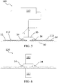
- Exemplary Fig. 6 shows one exemplary embodiment of a control mechanism as described above and shown schematically in exemplary Fig. 5 .
- One exemplary embodiment of a control mechanism 120 is a thermo-compression process using heated blocks 122. Thermo-compression is a process by which an RFID chip 20 is pressed into a mount, for example strap 30, with an adhesive 34. The pressure may be applied by heated blocks 122.
- a measurement system as shown in exemplary Fig. 5 and described above, may be used in conjunction with heated blocks 122 to achieve a desired z-direction spacing between the surface of an RFID chip 20 and pads 32, and thereby achieve a desired set of electrical properties of the resulting RFID strap 30.
- heated blocks 122 may cure adhesive 34. Heated blocks may be heated to temperatures of approximately 160-180°C.
- Exemplary Fig. 7 refers generally to exemplary Figs 5-6 .
- a flow diagram of feedback control system 100 using a control mechanism 120 similar to that as shown in exemplary Fig. 6 and described above may be shown.
- a chip assembly for example an RFID chip being assembled into an RFID strap.
- Measurement system 110 may then measure an electrical property in step 72, for example the parasitic capacitance of the chip.
- control mechanism 120 may increase or decrease pressure on the assembly.
- the desired C P is achieved in step 78, the pressure may be maintained while making the position of the chip static with respect to associated bond pads or curing of the adhesive completes.
- Curing may be accomplished either at the end of the process or continuously throughout the process. In the latter case, an efficient feedback system may be necessary to quickly determine and apply the correct amount of pressure.
- the present invention contemplates that curing may be accomplished by methods known in the art and/or the following methods: using a hot melt adhesive, where the chip is moved when the chip is hot, and the position of the chip is made static by cooling; using a UV or other photo-curable adhesive; and/or using a two-part adhesive where the position is changed when the first part adhesive is in its liquid state but the adhesive is cured by application of a second material such as an accelerator or even using a structural adhesive which forms a temporary bond and then after time or exposure to heat or other energy becomes permanent.
- a hot melt adhesive where the chip is moved when the chip is hot, and the position of the chip is made static by cooling
- a UV or other photo-curable adhesive and/or using a two-part adhesive where the position is changed when the first part adhesive is in its liquid state but the adhesive is cured by application of
- the present invention also contemplates that curing may take place using a non adhesive implementation such as using a solder in which the chip is moved with the solder in its molten state and the position is fixed by cooling.
- a non adhesive implementation such as using a solder in which the chip is moved with the solder in its molten state and the position is fixed by cooling.
- the position of a static chip does not need to utilize an adhesive.
- various forms of welding, such as ultrasonic and thermosonic could be used in a non adhesive implementation.
- a secondary operation may apply a material, such as a silicone referred to as a "blob top" to protect the chip and bond it.
- an alternative embodiment of a feedback control system 200 may be used when an RFID chip 20 is mounted on an antenna 202.
- Antenna 202 may have a central loop section 204 which may resonate with the parasitic capacitance C P of mounted RFID chip 20.
- the magnetic adsorption frequency of the central loop section 204 is measured by measurement system 210.
- Measurement system 210 may be communicatively coupled with adjustment system 220, which may create or adjust a force F on chip 20 in any of the x, y, or z axes to control the location, placement, and/or spacing of chip 20.
- a feedback control system 300 may be used to calculate statistical information regarding multiple RFID chip assemblies, such as RFID straps, RFID antennas, or as desired.
- a chip attach system 310 may attach RFID chips to antennas or straps on a web. The web may then carry the assemblies to a measurement system 320, which may be similar to measurement system 110 as shown in exemplary Fig. 5 and described above.
- a computer 330 may then calculate the average parasitic capacitance C P and its standard deviation SD, if desired. Other statistical calculations may also be done, however only these two will be followed for clarity in this example.
- the calculated average C P and SD may then be used to adjust the parameters used in chip attach system 310.
- the adjustment of the parameters of chip attach system 310 may be done on a dynamic basis without pausing production, which may allow for real-time feedback between the adjustment and measurements by measurement system 320.
- an RFID chip attach system may include at least one RFID chip, a feedback control system similar to any as described above, and a substrate for strap, antenna, or any other suitable assembly type, as desired.
- the RFID chip in this embodiment which may be similar to RFID chip 10, may be designed and manufactured with a deliberately larger bonding area, allowing it to be attached to an assembly with poor dimensional stability. Though this characteristic is not often utilized in conventional manufacturing due to the resulting excessive variation in the assembly's electrical properties, in the chip attach system described herein, the feedback control system may dynamically control the resulting electrical properties, leading to less variation and a lower cost but still high-quality production process.
- data from repeated dynamic feedback adjustment-measurements relating to how a particular adjustment affects a particular characteristic, for example C P may be stored, analyzed, and utilized to create a mapping of the result of particular adjustments in any of the x, y, or z axes.
- the mapping can then be re-integrated into the feedback control system such that less integrations of adjustment-measurement may be needed, which may significantly speed up the production process.
- the present description is also valid for attaching a strap to an antenna, as the position of the strap could be dynamically altered over the chip pond pads. Pressure can be applied, and, in the case of capacitive attached the antenna bond pads could be designed to the joint capacitance which intentionally varies with position. For instance, the pads, in one embodiment, are narrower in the upper web direction compared to the further down position, so coupling capacitance, and hence the capacitance of the mounted strap is varied.
Landscapes
- Engineering & Computer Science (AREA)
- Microelectronics & Electronic Packaging (AREA)
- Physics & Mathematics (AREA)
- General Physics & Mathematics (AREA)
- Theoretical Computer Science (AREA)
- Computer Hardware Design (AREA)
- Artificial Intelligence (AREA)
- Computer Vision & Pattern Recognition (AREA)
- Details Of Aerials (AREA)
- Variable-Direction Aerials And Aerial Arrays (AREA)
- Arrangements For Transmission Of Measured Signals (AREA)
Applications Claiming Priority (3)
| Application Number | Priority Date | Filing Date | Title |
|---|---|---|---|
| US15/204,607 US10546226B2 (en) | 2016-07-07 | 2016-07-07 | Feedback control of mounted chip production |
| PCT/US2017/041071 WO2018009776A1 (en) | 2016-07-07 | 2017-07-07 | Feedback control of mounted chip production |
| EP17740260.9A EP3482339B1 (de) | 2016-07-07 | 2017-07-07 | Rückkopplungssteuerung der herstellung eines montierten chips |
Related Parent Applications (1)
| Application Number | Title | Priority Date | Filing Date |
|---|---|---|---|
| EP17740260.9A Division EP3482339B1 (de) | 2016-07-07 | 2017-07-07 | Rückkopplungssteuerung der herstellung eines montierten chips |
Publications (2)
| Publication Number | Publication Date |
|---|---|
| EP4036786A1 true EP4036786A1 (de) | 2022-08-03 |
| EP4036786B1 EP4036786B1 (de) | 2024-08-21 |
Family
ID=59351162
Family Applications (2)
| Application Number | Title | Priority Date | Filing Date |
|---|---|---|---|
| EP22163447.0A Active EP4036786B1 (de) | 2016-07-07 | 2017-07-07 | Rückkopplungssteuerung der herstellung eines montierten chips |
| EP17740260.9A Active EP3482339B1 (de) | 2016-07-07 | 2017-07-07 | Rückkopplungssteuerung der herstellung eines montierten chips |
Family Applications After (1)
| Application Number | Title | Priority Date | Filing Date |
|---|---|---|---|
| EP17740260.9A Active EP3482339B1 (de) | 2016-07-07 | 2017-07-07 | Rückkopplungssteuerung der herstellung eines montierten chips |
Country Status (4)
| Country | Link |
|---|---|
| US (1) | US10546226B2 (de) |
| EP (2) | EP4036786B1 (de) |
| CN (1) | CN109643361B (de) |
| WO (1) | WO2018009776A1 (de) |
Citations (3)
| Publication number | Priority date | Publication date | Assignee | Title |
|---|---|---|---|---|
| US20050282495A1 (en) * | 2004-06-18 | 2005-12-22 | Forster Ian J | Method of variable position strap mounting for RFID transponder |
| US20160003895A1 (en) * | 2014-07-07 | 2016-01-07 | Avery Dennison Corporation | System and method for capacitive coupling testing |
| US20160034807A1 (en) * | 2014-08-04 | 2016-02-04 | Avery Dennison Retail Information Services, Llc | Use of rfid chip as assembly facilitator |
Family Cites Families (12)
| Publication number | Priority date | Publication date | Assignee | Title |
|---|---|---|---|---|
| US7225992B2 (en) * | 2003-02-13 | 2007-06-05 | Avery Dennison Corporation | RFID device tester and method |
| US7176799B1 (en) * | 2003-12-04 | 2007-02-13 | George Schmitt & Company | Assembling pressure sensitive labels with RFID tags |
| DE602005021823D1 (de) * | 2004-12-22 | 2010-07-22 | Texas Instruments Deutschland | Verfahren und vorrichtung zum kontaktlosen prüfen von rfid-schlaufen |
| US7225537B2 (en) * | 2005-01-27 | 2007-06-05 | Cardxx, Inc. | Method for making memory cards and similar devices using isotropic thermoset materials with high quality exterior surfaces |
| US7301458B2 (en) * | 2005-05-11 | 2007-11-27 | Alien Technology Corporation | Method and apparatus for testing RFID devices |
| US7456748B2 (en) * | 2005-10-20 | 2008-11-25 | National Starch And Chemical Investment Holding Corporation | RFID antenna with pre-applied adhesives |
| US7635014B2 (en) * | 2005-11-11 | 2009-12-22 | Semiconductor Energy Laboratory Co., Ltd. | Method for pressure bonding and method for manufacturing semiconductor device |
| DE102006007423A1 (de) * | 2005-11-17 | 2007-05-31 | Mühlbauer Ag | Vorrichtung und Verfahren zum Testen der Lesezuverlässigkeit von Smart Labels |
| WO2012012696A2 (en) * | 2010-07-22 | 2012-01-26 | Hm Energy, Llc | Surface acoustic wave transponder package for down-hole applications |
| US8884764B2 (en) * | 2011-02-25 | 2014-11-11 | Avery Dennison Corporation | Method, system, and apparatus for RFID removal detection |
| EP2788920B2 (de) * | 2011-12-09 | 2021-04-14 | Avery Dennison Corporation | Rfid-digitaldruck und -kodierung |
| US9857413B2 (en) * | 2014-07-02 | 2018-01-02 | Avery Dennison Retail Information Services, Llc | Systems and methods for testing RFID straps |
-
2016
- 2016-07-07 US US15/204,607 patent/US10546226B2/en active Active
-
2017
- 2017-07-07 EP EP22163447.0A patent/EP4036786B1/de active Active
- 2017-07-07 WO PCT/US2017/041071 patent/WO2018009776A1/en not_active Ceased
- 2017-07-07 EP EP17740260.9A patent/EP3482339B1/de active Active
- 2017-07-07 CN CN201780052047.4A patent/CN109643361B/zh active Active
Patent Citations (3)
| Publication number | Priority date | Publication date | Assignee | Title |
|---|---|---|---|---|
| US20050282495A1 (en) * | 2004-06-18 | 2005-12-22 | Forster Ian J | Method of variable position strap mounting for RFID transponder |
| US20160003895A1 (en) * | 2014-07-07 | 2016-01-07 | Avery Dennison Corporation | System and method for capacitive coupling testing |
| US20160034807A1 (en) * | 2014-08-04 | 2016-02-04 | Avery Dennison Retail Information Services, Llc | Use of rfid chip as assembly facilitator |
Also Published As
| Publication number | Publication date |
|---|---|
| CN109643361A (zh) | 2019-04-16 |
| EP3482339A1 (de) | 2019-05-15 |
| US10546226B2 (en) | 2020-01-28 |
| US20180012116A1 (en) | 2018-01-11 |
| EP4036786B1 (de) | 2024-08-21 |
| EP3482339B1 (de) | 2022-03-30 |
| CN109643361B (zh) | 2022-03-15 |
| WO2018009776A1 (en) | 2018-01-11 |
Similar Documents
| Publication | Publication Date | Title |
|---|---|---|
| US9874603B2 (en) | System and method for capacitive coupling testing | |
| US9373070B2 (en) | Use of RFID chip as assembly facilitator | |
| CN102208045B (zh) | 分体式无源电子标签及采用该标签的印制电路板 | |
| EP1796027A1 (de) | RFID Vorrichtung | |
| US20160042204A1 (en) | System and method for testing performance of mobile radio frequency identification tag | |
| CN104487985B (zh) | Rfid标签的检查方法及检查装置 | |
| US8770836B2 (en) | Wireless temperature profiling system | |
| CN101142491A (zh) | Rfid应用测试系统和方法 | |
| US20120126945A1 (en) | Strong passive ad-hoc rado-frequency identification | |
| Jaakkola et al. | Near-field UHF RFID transponder with a screen-printed graphene antenna | |
| US11039538B2 (en) | Communication system including antennas on flexible circuit board | |
| CN115372384B (zh) | 射频检测系统及其裂纹、应变检测方法和rfid标签 | |
| JP6229265B2 (ja) | Rfidタグシステム及び温度検出方法 | |
| EP4036786B1 (de) | Rückkopplungssteuerung der herstellung eines montierten chips | |
| Jankowski-Mihułowicz et al. | Flexible antenna design for semi-passive HF RFID transponder in ink-jet technology | |
| US7375633B2 (en) | Methods and systems for in-line RFID transponder testing | |
| CN101536344A (zh) | 用于近场和远场无线射频识别的天线 | |
| US20110024326A1 (en) | Ic package tray embedded rfid | |
| CN101636744A (zh) | 非接触式传输元件以及对其进行表征的方法 | |
| CN202084068U (zh) | 分体式无源rfid标签及采用该标签的印制电路板 | |
| US8228075B2 (en) | Test system for radio frequency IC devices and method of manufacturing radio frequency IC devices using the same | |
| Le et al. | A comparison of printed flexible RFID/NFC antennas for a microelectronic measurement system | |
| US10467514B1 (en) | Method for combining RFID tags | |
| CN208110608U (zh) | 射频识别隧道测试装置 | |
| CN205281546U (zh) | 一种具备温度传感功能的无源超高频标签 |
Legal Events
| Date | Code | Title | Description |
|---|---|---|---|
| PUAI | Public reference made under article 153(3) epc to a published international application that has entered the european phase |
Free format text: ORIGINAL CODE: 0009012 |
|
| STAA | Information on the status of an ep patent application or granted ep patent |
Free format text: STATUS: THE APPLICATION HAS BEEN PUBLISHED |
|
| AC | Divisional application: reference to earlier application |
Ref document number: 3482339 Country of ref document: EP Kind code of ref document: P |
|
| AK | Designated contracting states |
Kind code of ref document: A1 Designated state(s): AL AT BE BG CH CY CZ DE DK EE ES FI FR GB GR HR HU IE IS IT LI LT LU LV MC MK MT NL NO PL PT RO RS SE SI SK SM TR |
|
| STAA | Information on the status of an ep patent application or granted ep patent |
Free format text: STATUS: REQUEST FOR EXAMINATION WAS MADE |
|
| 17P | Request for examination filed |
Effective date: 20230126 |
|
| RBV | Designated contracting states (corrected) |
Designated state(s): AL AT BE BG CH CY CZ DE DK EE ES FI FR GB GR HR HU IE IS IT LI LT LU LV MC MK MT NL NO PL PT RO RS SE SI SK SM TR |
|
| GRAP | Despatch of communication of intention to grant a patent |
Free format text: ORIGINAL CODE: EPIDOSNIGR1 |
|
| STAA | Information on the status of an ep patent application or granted ep patent |
Free format text: STATUS: GRANT OF PATENT IS INTENDED |
|
| INTG | Intention to grant announced |
Effective date: 20240219 |
|
| GRAS | Grant fee paid |
Free format text: ORIGINAL CODE: EPIDOSNIGR3 |
|
| P01 | Opt-out of the competence of the unified patent court (upc) registered |
Effective date: 20240426 |
|
| GRAA | (expected) grant |
Free format text: ORIGINAL CODE: 0009210 |
|
| STAA | Information on the status of an ep patent application or granted ep patent |
Free format text: STATUS: THE PATENT HAS BEEN GRANTED |
|
| AC | Divisional application: reference to earlier application |
Ref document number: 3482339 Country of ref document: EP Kind code of ref document: P |
|
| AK | Designated contracting states |
Kind code of ref document: B1 Designated state(s): AL AT BE BG CH CY CZ DE DK EE ES FI FR GB GR HR HU IE IS IT LI LT LU LV MC MK MT NL NO PL PT RO RS SE SI SK SM TR |
|
| REG | Reference to a national code |
Ref country code: GB Ref legal event code: FG4D |
|
| REG | Reference to a national code |
Ref country code: CH Ref legal event code: EP |
|
| REG | Reference to a national code |
Ref country code: IE Ref legal event code: FG4D |
|
| REG | Reference to a national code |
Ref country code: DE Ref legal event code: R096 Ref document number: 602017084397 Country of ref document: DE |
|
| REG | Reference to a national code |
Ref country code: LT Ref legal event code: MG9D |
|
| REG | Reference to a national code |
Ref country code: NL Ref legal event code: MP Effective date: 20240821 |
|
| PG25 | Lapsed in a contracting state [announced via postgrant information from national office to epo] |
Ref country code: NO Free format text: LAPSE BECAUSE OF FAILURE TO SUBMIT A TRANSLATION OF THE DESCRIPTION OR TO PAY THE FEE WITHIN THE PRESCRIBED TIME-LIMIT Effective date: 20241121 |
|
| REG | Reference to a national code |
Ref country code: AT Ref legal event code: MK05 Ref document number: 1716217 Country of ref document: AT Kind code of ref document: T Effective date: 20240821 |
|
| PG25 | Lapsed in a contracting state [announced via postgrant information from national office to epo] |
Ref country code: FI Free format text: LAPSE BECAUSE OF FAILURE TO SUBMIT A TRANSLATION OF THE DESCRIPTION OR TO PAY THE FEE WITHIN THE PRESCRIBED TIME-LIMIT Effective date: 20240821 Ref country code: PT Free format text: LAPSE BECAUSE OF FAILURE TO SUBMIT A TRANSLATION OF THE DESCRIPTION OR TO PAY THE FEE WITHIN THE PRESCRIBED TIME-LIMIT Effective date: 20241223 Ref country code: NL Free format text: LAPSE BECAUSE OF FAILURE TO SUBMIT A TRANSLATION OF THE DESCRIPTION OR TO PAY THE FEE WITHIN THE PRESCRIBED TIME-LIMIT Effective date: 20240821 Ref country code: PL Free format text: LAPSE BECAUSE OF FAILURE TO SUBMIT A TRANSLATION OF THE DESCRIPTION OR TO PAY THE FEE WITHIN THE PRESCRIBED TIME-LIMIT Effective date: 20240821 Ref country code: GR Free format text: LAPSE BECAUSE OF FAILURE TO SUBMIT A TRANSLATION OF THE DESCRIPTION OR TO PAY THE FEE WITHIN THE PRESCRIBED TIME-LIMIT Effective date: 20241122 |
|
| PG25 | Lapsed in a contracting state [announced via postgrant information from national office to epo] |
Ref country code: BG Free format text: LAPSE BECAUSE OF FAILURE TO SUBMIT A TRANSLATION OF THE DESCRIPTION OR TO PAY THE FEE WITHIN THE PRESCRIBED TIME-LIMIT Effective date: 20240821 |
|
| PG25 | Lapsed in a contracting state [announced via postgrant information from national office to epo] |
Ref country code: LV Free format text: LAPSE BECAUSE OF FAILURE TO SUBMIT A TRANSLATION OF THE DESCRIPTION OR TO PAY THE FEE WITHIN THE PRESCRIBED TIME-LIMIT Effective date: 20240821 |
|
| PG25 | Lapsed in a contracting state [announced via postgrant information from national office to epo] |
Ref country code: AT Free format text: LAPSE BECAUSE OF FAILURE TO SUBMIT A TRANSLATION OF THE DESCRIPTION OR TO PAY THE FEE WITHIN THE PRESCRIBED TIME-LIMIT Effective date: 20240821 Ref country code: IS Free format text: LAPSE BECAUSE OF FAILURE TO SUBMIT A TRANSLATION OF THE DESCRIPTION OR TO PAY THE FEE WITHIN THE PRESCRIBED TIME-LIMIT Effective date: 20241221 |
|
| PG25 | Lapsed in a contracting state [announced via postgrant information from national office to epo] |
Ref country code: HR Free format text: LAPSE BECAUSE OF FAILURE TO SUBMIT A TRANSLATION OF THE DESCRIPTION OR TO PAY THE FEE WITHIN THE PRESCRIBED TIME-LIMIT Effective date: 20240821 |
|
| PG25 | Lapsed in a contracting state [announced via postgrant information from national office to epo] |
Ref country code: ES Free format text: LAPSE BECAUSE OF FAILURE TO SUBMIT A TRANSLATION OF THE DESCRIPTION OR TO PAY THE FEE WITHIN THE PRESCRIBED TIME-LIMIT Effective date: 20240821 Ref country code: RS Free format text: LAPSE BECAUSE OF FAILURE TO SUBMIT A TRANSLATION OF THE DESCRIPTION OR TO PAY THE FEE WITHIN THE PRESCRIBED TIME-LIMIT Effective date: 20241121 |
|
| PG25 | Lapsed in a contracting state [announced via postgrant information from national office to epo] |
Ref country code: RS Free format text: LAPSE BECAUSE OF FAILURE TO SUBMIT A TRANSLATION OF THE DESCRIPTION OR TO PAY THE FEE WITHIN THE PRESCRIBED TIME-LIMIT Effective date: 20241121 Ref country code: PT Free format text: LAPSE BECAUSE OF FAILURE TO SUBMIT A TRANSLATION OF THE DESCRIPTION OR TO PAY THE FEE WITHIN THE PRESCRIBED TIME-LIMIT Effective date: 20241223 Ref country code: PL Free format text: LAPSE BECAUSE OF FAILURE TO SUBMIT A TRANSLATION OF THE DESCRIPTION OR TO PAY THE FEE WITHIN THE PRESCRIBED TIME-LIMIT Effective date: 20240821 Ref country code: NO Free format text: LAPSE BECAUSE OF FAILURE TO SUBMIT A TRANSLATION OF THE DESCRIPTION OR TO PAY THE FEE WITHIN THE PRESCRIBED TIME-LIMIT Effective date: 20241121 Ref country code: NL Free format text: LAPSE BECAUSE OF FAILURE TO SUBMIT A TRANSLATION OF THE DESCRIPTION OR TO PAY THE FEE WITHIN THE PRESCRIBED TIME-LIMIT Effective date: 20240821 Ref country code: LV Free format text: LAPSE BECAUSE OF FAILURE TO SUBMIT A TRANSLATION OF THE DESCRIPTION OR TO PAY THE FEE WITHIN THE PRESCRIBED TIME-LIMIT Effective date: 20240821 Ref country code: IS Free format text: LAPSE BECAUSE OF FAILURE TO SUBMIT A TRANSLATION OF THE DESCRIPTION OR TO PAY THE FEE WITHIN THE PRESCRIBED TIME-LIMIT Effective date: 20241221 Ref country code: HR Free format text: LAPSE BECAUSE OF FAILURE TO SUBMIT A TRANSLATION OF THE DESCRIPTION OR TO PAY THE FEE WITHIN THE PRESCRIBED TIME-LIMIT Effective date: 20240821 Ref country code: GR Free format text: LAPSE BECAUSE OF FAILURE TO SUBMIT A TRANSLATION OF THE DESCRIPTION OR TO PAY THE FEE WITHIN THE PRESCRIBED TIME-LIMIT Effective date: 20241122 Ref country code: FI Free format text: LAPSE BECAUSE OF FAILURE TO SUBMIT A TRANSLATION OF THE DESCRIPTION OR TO PAY THE FEE WITHIN THE PRESCRIBED TIME-LIMIT Effective date: 20240821 Ref country code: ES Free format text: LAPSE BECAUSE OF FAILURE TO SUBMIT A TRANSLATION OF THE DESCRIPTION OR TO PAY THE FEE WITHIN THE PRESCRIBED TIME-LIMIT Effective date: 20240821 Ref country code: BG Free format text: LAPSE BECAUSE OF FAILURE TO SUBMIT A TRANSLATION OF THE DESCRIPTION OR TO PAY THE FEE WITHIN THE PRESCRIBED TIME-LIMIT Effective date: 20240821 Ref country code: AT Free format text: LAPSE BECAUSE OF FAILURE TO SUBMIT A TRANSLATION OF THE DESCRIPTION OR TO PAY THE FEE WITHIN THE PRESCRIBED TIME-LIMIT Effective date: 20240821 |
|
| PG25 | Lapsed in a contracting state [announced via postgrant information from national office to epo] |
Ref country code: DK Free format text: LAPSE BECAUSE OF FAILURE TO SUBMIT A TRANSLATION OF THE DESCRIPTION OR TO PAY THE FEE WITHIN THE PRESCRIBED TIME-LIMIT Effective date: 20240821 Ref country code: SM Free format text: LAPSE BECAUSE OF FAILURE TO SUBMIT A TRANSLATION OF THE DESCRIPTION OR TO PAY THE FEE WITHIN THE PRESCRIBED TIME-LIMIT Effective date: 20240821 Ref country code: RO Free format text: LAPSE BECAUSE OF FAILURE TO SUBMIT A TRANSLATION OF THE DESCRIPTION OR TO PAY THE FEE WITHIN THE PRESCRIBED TIME-LIMIT Effective date: 20240821 |
|
| PG25 | Lapsed in a contracting state [announced via postgrant information from national office to epo] |
Ref country code: EE Free format text: LAPSE BECAUSE OF FAILURE TO SUBMIT A TRANSLATION OF THE DESCRIPTION OR TO PAY THE FEE WITHIN THE PRESCRIBED TIME-LIMIT Effective date: 20240821 |
|
| PG25 | Lapsed in a contracting state [announced via postgrant information from national office to epo] |
Ref country code: CZ Free format text: LAPSE BECAUSE OF FAILURE TO SUBMIT A TRANSLATION OF THE DESCRIPTION OR TO PAY THE FEE WITHIN THE PRESCRIBED TIME-LIMIT Effective date: 20240821 |
|
| PG25 | Lapsed in a contracting state [announced via postgrant information from national office to epo] |
Ref country code: IT Free format text: LAPSE BECAUSE OF FAILURE TO SUBMIT A TRANSLATION OF THE DESCRIPTION OR TO PAY THE FEE WITHIN THE PRESCRIBED TIME-LIMIT Effective date: 20240821 Ref country code: SK Free format text: LAPSE BECAUSE OF FAILURE TO SUBMIT A TRANSLATION OF THE DESCRIPTION OR TO PAY THE FEE WITHIN THE PRESCRIBED TIME-LIMIT Effective date: 20240821 |
|
| REG | Reference to a national code |
Ref country code: DE Ref legal event code: R097 Ref document number: 602017084397 Country of ref document: DE |
|
| PLBE | No opposition filed within time limit |
Free format text: ORIGINAL CODE: 0009261 |
|
| STAA | Information on the status of an ep patent application or granted ep patent |
Free format text: STATUS: NO OPPOSITION FILED WITHIN TIME LIMIT |
|
| PGFP | Annual fee paid to national office [announced via postgrant information from national office to epo] |
Ref country code: GB Payment date: 20250612 Year of fee payment: 9 |
|
| PGFP | Annual fee paid to national office [announced via postgrant information from national office to epo] |
Ref country code: FR Payment date: 20250612 Year of fee payment: 9 |
|
| 26N | No opposition filed |
Effective date: 20250522 |
|
| PG25 | Lapsed in a contracting state [announced via postgrant information from national office to epo] |
Ref country code: SE Free format text: LAPSE BECAUSE OF FAILURE TO SUBMIT A TRANSLATION OF THE DESCRIPTION OR TO PAY THE FEE WITHIN THE PRESCRIBED TIME-LIMIT Effective date: 20240821 |
|
| PGFP | Annual fee paid to national office [announced via postgrant information from national office to epo] |
Ref country code: DE Payment date: 20250616 Year of fee payment: 9 |
|
| REG | Reference to a national code |
Ref country code: CH Ref legal event code: H13 Free format text: ST27 STATUS EVENT CODE: U-0-0-H10-H13 (AS PROVIDED BY THE NATIONAL OFFICE) Effective date: 20260224 |
|
| PG25 | Lapsed in a contracting state [announced via postgrant information from national office to epo] |
Ref country code: LU Free format text: LAPSE BECAUSE OF NON-PAYMENT OF DUE FEES Effective date: 20250707 |
|
| REG | Reference to a national code |
Ref country code: BE Ref legal event code: MM Effective date: 20250731 |
|
| PG25 | Lapsed in a contracting state [announced via postgrant information from national office to epo] |
Ref country code: BE Free format text: LAPSE BECAUSE OF NON-PAYMENT OF DUE FEES Effective date: 20250731 |
|
| PG25 | Lapsed in a contracting state [announced via postgrant information from national office to epo] |
Ref country code: CH Free format text: LAPSE BECAUSE OF NON-PAYMENT OF DUE FEES Effective date: 20250731 |