EP4036587B1 - Multipfad-breitband-stromsensor - Google Patents
Multipfad-breitband-stromsensor Download PDFInfo
- Publication number
- EP4036587B1 EP4036587B1 EP21213675.8A EP21213675A EP4036587B1 EP 4036587 B1 EP4036587 B1 EP 4036587B1 EP 21213675 A EP21213675 A EP 21213675A EP 4036587 B1 EP4036587 B1 EP 4036587B1
- Authority
- EP
- European Patent Office
- Prior art keywords
- magnetic field
- current
- signal
- coil
- current sensor
- Prior art date
- Legal status (The legal status is an assumption and is not a legal conclusion. Google has not performed a legal analysis and makes no representation as to the accuracy of the status listed.)
- Active
Links
Images




Classifications
-
- G—PHYSICS
- G01—MEASURING; TESTING
- G01R—MEASURING ELECTRIC VARIABLES; MEASURING MAGNETIC VARIABLES
- G01R15/00—Details of measuring arrangements of the types provided for in groups G01R17/00 - G01R29/00, G01R33/00 - G01R33/26 or G01R35/00
- G01R15/14—Adaptations providing voltage or current isolation, e.g. for high-voltage or high-current networks
- G01R15/142—Arrangements for simultaneous measurements of several parameters employing techniques covered by groups G01R15/14 - G01R15/26
-
- G—PHYSICS
- G01—MEASURING; TESTING
- G01R—MEASURING ELECTRIC VARIABLES; MEASURING MAGNETIC VARIABLES
- G01R19/00—Arrangements for measuring currents or voltages or for indicating presence or sign thereof
- G01R19/14—Indicating direction of current; Indicating polarity of voltage
-
- G—PHYSICS
- G01—MEASURING; TESTING
- G01R—MEASURING ELECTRIC VARIABLES; MEASURING MAGNETIC VARIABLES
- G01R15/00—Details of measuring arrangements of the types provided for in groups G01R17/00 - G01R29/00, G01R33/00 - G01R33/26 or G01R35/00
- G01R15/14—Adaptations providing voltage or current isolation, e.g. for high-voltage or high-current networks
- G01R15/18—Adaptations providing voltage or current isolation, e.g. for high-voltage or high-current networks using inductive devices, e.g. transformers
- G01R15/181—Adaptations providing voltage or current isolation, e.g. for high-voltage or high-current networks using inductive devices, e.g. transformers using coils without a magnetic core, e.g. Rogowski coils
-
- G—PHYSICS
- G01—MEASURING; TESTING
- G01R—MEASURING ELECTRIC VARIABLES; MEASURING MAGNETIC VARIABLES
- G01R15/00—Details of measuring arrangements of the types provided for in groups G01R17/00 - G01R29/00, G01R33/00 - G01R33/26 or G01R35/00
- G01R15/14—Adaptations providing voltage or current isolation, e.g. for high-voltage or high-current networks
- G01R15/20—Adaptations providing voltage or current isolation, e.g. for high-voltage or high-current networks using galvano-magnetic devices, e.g. Hall-effect devices, i.e. measuring a magnetic field via the interaction between a current and a magnetic field, e.g. magneto resistive or Hall effect devices
- G01R15/207—Constructional details independent of the type of device used
-
- G—PHYSICS
- G01—MEASURING; TESTING
- G01R—MEASURING ELECTRIC VARIABLES; MEASURING MAGNETIC VARIABLES
- G01R19/00—Arrangements for measuring currents or voltages or for indicating presence or sign thereof
- G01R19/25—Arrangements for measuring currents or voltages or for indicating presence or sign thereof using digital measurement techniques
Definitions
- This disclosure relates generally to current sensors and more particularly to multipath wide bandwidth current sensor integrated circuits (ICs).
- Some electrical current sensors use one or more magnetic field sensing elements in proximity to a current-carrying conductor to sense a magnetic field generated by the current.
- the magnetic field sensing elements generate an output signal having a magnitude proportional to the magnetic field induced by the current through the conductor.
- the current conductor includes a loop formed by the lead frame.
- US 2019/0346515 A1 relates to a magnetic field sensor apparatus comprising a coil and a magnetic field sensor.
- a chip carrying the coil and the magnetic field sensor is arranged on a leadframe, the leadframe comprising a cutout.
- US 2008/0297138 A1 relates to an integrated circuit current sensor that includes a lead frame having at least two leads coupled to provide a current conductor portion, and a substrate having a first surface in which is disposed one or more magnetic field sensing elements, with the first surface being proximate to the current conductor portion and a second surface distal from the current conductor position.
- JIANG JUNFENG ET AL A Hybrid Multi-Path CMOS Magnetic sensor With 76 ppm/°C Sensitivity Drift and Discrete-Time Ripple Reduction Loops " relates to a temperature-insensitive magnetic sensor system for contactless current measurements.
- the system employs a multi-path structure with a set of spinning current Hall sensors in its low-frequency path and a set of pick-up coils in its high frequency path.
- Current sensors sometimes employ a combination of a magnetic field transducer, such as a Hall effect element, for sensing relatively low frequency content of the current and an inductive pickup coil for sensing higher frequency content of the current in order to thereby sense a broader current bandwidth.
- a magnetic field transducer such as a Hall effect element
- an inductive pickup coil for sensing higher frequency content of the current in order to thereby sense a broader current bandwidth.
- offset compensation associated with an integrator in the coil signal path requires complex matching of poles and zeros and use of large components that require "off-chip” implementation (i.e., outside of the integrated circuit package).
- Described herein are current sensor structures and methods directed towards providing wide bandwidth current sensor integrated circuits (ICs) having a magnetic field transducer path for sensing lower frequencies and an inductive coil path for sensing higher frequencies. Placement of transducer/coil pairs on opposite sides of the current conductor provides stray field immunity and positioning of the transducers within a respective coil maximizes coupling so as to reduce susceptibility to sensing variations due to manufacturing position tolerances.
- the coils can be provided in a "figure eight" pattern in order to reduce the effect of stray fields on common mode voltage variations.
- One or more electromagnetic shields reduce the effects of capacitive coupling to the sensing elements, substrate, and circuitry.
- the low frequency signal path can include an impulse filter to remove impulse disturbances.
- offset is compensated with circuitry in a manner that permits on-chip implementation (thereby reducing cost and size disadvantages of some previous current sensor designs) and eliminates the need for complex zero/pole matching (which presents a challenge in some previous current sensor designs). Further, startup performance of the compensation circuitry is optimized using a switched capacitor network or a MOSFET-C circuit.
- a current sensor includes a lead frame having a plurality of leads, at least two of the plurality of leads forming a current conductor configured to carry a current that generates a magnetic field and a substrate having first and second opposing surfaces, the first surface proximate to said current conductor and the second surface distal from the current conductor.
- a first magnetic field transducer is disposed on the substrate and a first coil is disposed on the substrate adjacent to the first magnetic field transducer, wherein the first magnetic field transducer and the first coil are positioned on a first side of the current conductor.
- a second magnetic field transducer is disposed on the substrate and a second coil is disposed on the substrate adjacent to the second magnetic field transducer, wherein the second magnetic field transducer and the second coil are positioned on a second side of the current conductor.
- the current conductor may be curved and wherein the first side of the current conductor is inside the curve and the second side of the current conductor is outside the curve.
- the first coil may be disposed concentrically with respect to the first magnetic field transducer and the second coil may be disposed concentrically with respect to the second magnetic field transducer.
- the first magnetic field transducer and the second magnetic field transducer may be disposed on the first surface of the substrate.
- the current sensor may further include a shield disposed between the current conductor and the first and second coils, wherein the shield has at least one feature selected to reduce an eddy current induced in the shield.
- the shield may include at least one slot configured to reduce a path length of a closed loop current path in the shield.
- the current sensor may further include a second shield disposed between the first and second coils and the second surface of the substrate.
- the first coil includes third and fourth coils wound in opposite directions with respect to each other and the second coil includes fifth and sixth coils wound in opposite directions with respect to each other.
- the first and second magnetic field transducers may each include a Hall effect element.
- the first magnetic field transducer can generate a first magnetic field signal
- the second magnetic field transducer can generate a second magnetic field signal
- the first coil can generate a third magnetic field signal
- the second coil can generate a fourth magnetic field signal
- the current sensor may include a first signal path coupled to receive the first and second magnetic field signals and configured to generate a low frequency signal associated with a low frequency content of the current through the current conductor and a second signal path coupled to receive the third and fourth magnetic field signals and configured to generate a high frequency signal associated with a high frequency content of the current through the current conductor.
- a summation circuit can be configured to sum the low frequency signal and the high frequency signal to provide a signal indicative of the current through the conductor.
- the first magnetic field transducer and the second magnetic field transducer may detect the magnetic field in opposite directions and the first coil and the second coil may detect the magnetic field in opposite directions, wherein the low frequency signal is a differential signal generated by subtraction of the second magnetic field signal from the first magnetic field signal and the high frequency signal is a differential signal generated by subtraction of the fourth magnetic field signal from the third magnetic field signal.
- the first signal path may include a dV/dt filter responsive to the first and second magnetic field signals and configured to generate an impulse filtered signal.
- a low pass filter can be coupled to receive the impulse filtered signal and generate the low frequency signal.
- the dV/dt filter can be a median filter.
- the second signal path can include an integrator coupled to receive the third and fourth magnetic field signals and an amplifier with an offset rejection circuit coupled in a feedback relationship between an output and an input of the amplifier.
- the offset rejection circuit can include a proportional-integral circuit configured to compensate for an offset of the amplifier.
- the proportional-integral circuit may include an integrator stage having an integrating amplifier with a feedback capacitor and a first input resistor, wherein a time constant of the integrator is established by a capacitance of the feedback capacitor and an effective resistance of the first input resistor and a proportional stage including an amplifier having a second input resistor and a feedback resistor.
- the first input resistor may include a fixed resistor and a switched capacitor circuit having a plurality of switches and a capacitor.
- the plurality of switches of the switched capacitor circuit may be controlled during a startup period to decrease the effective resistance of the first input resistor in order to thereby decrease the time constant of the integrator and may be controlled following the startup period to increase the effective resistance of the first input resistor in order to thereby increase the time constant of the integrator.
- the first input resistor may include a fixed resistor and a MOSFET-C circuit comprising a plurality of MOSFETs and one or more switches coupled in parallel with the plurality of MOSFETs.
- the one or more switches of the MOSFET-C circuit may be controlled during a startup period to decrease the effective resistance of the first input resistor in order to thereby decrease the time constant of the integrator and may be controlled following the startup period to increase the effective resistance of the first input resistor in order to thereby increase the time constant of the integrator.
- the current sensor may include an integrated circuit package configured to enclose the substrate and at least a portion of the plurality of leads of the lead frame.
- a current sensor including a lead frame having a plurality of leads, at least two of the plurality of leads forming a current conductor configured to carry a current that generates a magnetic field and a substrate having first and second opposing surfaces, the first surface proximate to said current conductor and the second surface distal from the current conductor.
- a first magnetic field transducer disposed on the substrate is configured to generate a first magnetic field signal and a first coil is disposed on the substrate concentrically with respect to the first magnetic field transducer and configured to generate a second magnetic field signal.
- a first signal path coupled to receive the first magnetic field signal is configured to generate a low frequency signal associated with a low frequency content of the current through the current conductor and a second signal path coupled to receive the second magnetic field signal is configured to generate a high frequency signal associated with a high frequency content of the current through the current conductor.
- a summation circuit is configured to sum the low frequency signal and the high frequency signal to provide a signal indicative of the current through the current conductor.
- a current sensor includes a lead frame having a plurality of leads, at least two of the plurality of leads forming a current conductor configured to carry a current that generates a magnetic field and a substrate having first and second opposing surfaces, the first surface proximate to said current conductor and the second surface distal from the current conductor.
- a first magnetic field transducer is disposed on the substrate and a first coil is disposed on the substrate adjacent to the first magnetic field transducer.
- a second magnetic field transducer is disposed on the substrate and a second coil is disposed on the substrate adjacent to the second magnetic field transducer.
- the first coil includes third and fourth coils wound in opposite directions with respect to each other and the second coil includes fifth and sixth coils wound in opposite directions with respect to each other.
- a current sensor includes a lead frame having a plurality of leads, at least two of the plurality of leads forming a current conductor configured to carry a current that generates a magnetic field and a substrate having first and second opposing surfaces, the first surface proximate to said current conductor and the second surface distal from the current conductor.
- a first magnetic field transducer disposed on the substrate is configured to generate a first magnetic field signal and a first coil disposed on the substrate is configured to generate a second magnetic field signal.
- a first signal path coupled to receive the first magnetic field signal is configured to generate a low frequency signal associated with a low frequency content of the current through the current conductor, wherein the first signal path includes a dV/dt filter coupled to receive the first magnetic field signal and configured to generate an impulse filtered signal.
- a second signal path coupled to receive the second magnetic field signal is configured to generate a high frequency signal associated with a high frequency content of the current through the current conductor.
- a summation circuit is configured to sum the low frequency signal and the high frequency signal to provide a signal indicative of the current through the current conductor.
- a current sensor integrated circuit including a lead frame having a plurality of leads, at least two of the plurality of leads forming a current conductor configured to carry a current that generates a magnetic field and a substrate having first and second opposing surfaces, the first surface proximate to said current conductor and the second surface distal from the current conductor.
- a first magnetic field transducer disposed on the substrate is configured to generate a first magnetic field signal and a first coil disposed on the substrate is configured to generate a second magnetic field signal.
- a first signal path coupled to receive the first magnetic field signal is configured to generate a low frequency signal associated with a low frequency content of the current through the current conductor and a second signal path coupled to receive the second magnetic field signal is configured to generate a high frequency signal associated with a high frequency content of the current through the current conductor.
- the second signal path includes an integrator coupled to receive the second magnetic field signal and an amplifier having an offset rejection circuit coupled in a feedback relationship between an output and an input of the amplifier, wherein the offset rejection circuit includes a proportional-integral circuit configured to compensate for an offset of the amplifier.
- the proportional-integral circuit includes an integrator stage having an integrating amplifier with a feedback capacitor and a first input resistor, wherein a time constant of the integrator is established by a capacitance of the feedback capacitor and an effective resistance of the first input resistor.
- the proportional-integral circuit further includes a proportional stage including an amplifier having a second input resistor and a feedback resistor and a summation circuit configured to sum the low frequency signal and the high frequency signal to provide a signal indicative of the current through the current conductor.
- the first input resistor may include a fixed resistor and a MOSFET-C circuit comprising a plurality of MOSFETs and one or more switches coupled in parallel with the plurality of MOSFETs.
- the one or more switches of the MOSFET-C circuit may be controlled during a startup period to decrease the effective resistance of the first input resistor in order to thereby decrease the time constant of the integrator and may be controlled following the startup period to increase the effective resistance of the first input resistor in order to thereby increase the time constant of the integrator.
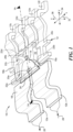
- a current sensor 10 includes a lead frame 12 having a plurality of leads 12a - 12f, at least two of which leads 12a, 12b form part of a current conductor 18 configured to carry a current (illustrated by arrow 28) that generates a magnetic field.
- a substrate 16 has first and second opposing surfaces 16a, 16b, with the first surface 16a proximate to the current conductor 18 and the second surface 16b distal from the current conductor.
- a first magnetic field transducer and coil pair 20a is disposed on the first surface 16a of the substrate 16 and a second magnetic field transducer and coil pair 20b is also disposed on the first surface 16a of the substrate 16.
- the substrate 16 is positioned with respect to the lead frame 12 such that the first transducer and coil pair 20a is positioned on a first side of the current conductor 18 and the second transducer and coil pair 20b is positioned on a second side of the current conductor.
- Conductor 18 includes leads 12a, 12b and a narrowed junction portion 14.
- the conductor portion 14 is curved and thus transducer/coil pair 20a can be described as being positioned "inside” the curve and transducer/coil pair 20b can be described as being positioned “outside” the curve.
- conductor 18 can include additional leads (not shown) based on application specifications.
- Signals from the first and second paths are combined (e.g., summed) to generate an output signal of the current sensor 10 that is indicative of the current 28 through the conductor 18 and that has a wider frequency bandwidth than possible with use of only magnetic field transducers or only inductive pickup coils.
- sensor 10 can sense current frequencies from DC to approximately 5MHz.
- transducer/coil pairs 20a, 20b placement of the transducer/coil pairs 20a, 20b on opposite sides of the conductor portion 14 and their design by which the pairs sense the magnetic field in opposite directions permit subtraction of their output signals to reject stray magnetic fields.
- a stray field i.e., not generated by the current in the lead frame 12
- the signals from the sensing elements are subtracted to determine the magnetic field generated by the current 28, any signal from a stray field will be removed.
- Substrate 16 can be comprised of a semiconductor material such as silicon (in which case substrate 16 can be referred to as a semiconductor die or simply die) or can be comprised of any suitable material for supporting electrical elements and signals, including insulating materials.
- Solder balls 22a - 22e on the substrate surface 16a can couple electrical elements of the current sensor disposed on or otherwise supported by the substrate to lead frame leads 12c - 12f (i.e., leads other than the conductor leads 12a, 12b, which leads 12c - 12f can be referred to as "signal leads"). While five solder balls 22a - 22e are shown, any number of solder balls can be provided, including dummy solder balls for mechanically stabilizing the substrate 16.
- solder balls 22a - 22e are shown, other connection methods can also be used, including, but not limited to gold bumps, eutectic or high lead solder bumps, no-lead solder bumps, gold stud bumps, polymeric conductive bumps, anisotropic conductive paste, conductive film, or wire bonds.
- wire bonds bond pads can be provided on the substrate and the wire bonds can be electrically connected between the bond pads and signal leads.
- the substrate 16 is arranged in a so-called "flip-chip" configuration with the active surface 16a (i.e., the surface supporting the transducer/coil pairs 20a, 20b) proximate to the conductor portion 14. This configuration positions the transducer/coil pairs 20a, 20b in close proximity to the conductor portion 14. It will be appreciated by those of ordinary skill in the art however, that in other embodiments, the substrate 16 can be inverted, or flipped by 180° to provide a so-called "die-up" configuration.
- Each transducer/coil pair 20a, 20b includes a magnetic field transducer and a conductive coil configured to sense magnetic field.
- the transducer of each pair 20a, 20b is a planar Hall effect element having a maximum response axis aligned with a z-axis 36.
- the transducer/coil pairs 20a, 20b are offset (along the y-axis 34) by substantially equal and opposite amounts with respect to the current conductor portion 14. It will be appreciated by those of ordinary skill in the art however, that the transducer/coil pairs 20a, 20b may alternatively be offset (along the y-axis 34) by unequal and opposite amounts with respect to the current conductor portion 14.
- the magnetic field sensing element can be, but is not limited to, a Hall effect element, a magnetoresistance element, or a magnetotransistor.
- a Hall effect element for example, a planar Hall element, a vertical Hall element, and a Circular Vertical Hall (CVH) element.
- CVH Circular Vertical Hall
- magnetoresistance elements for example, a semiconductor magnetoresistance element such as Indium Antimonide (InSb), a giant magnetoresistance (GMR) element, for example, a spin valve, an anisotropic magnetoresistance element (AMR), a tunneling magnetoresistance (TMR) element, and a magnetic tunnel junction (MTJ).
- the magnetic field sensing element may be a single element or, alternatively, may include two or more magnetic field sensing elements arranged in various configurations, e.g., a half-bridge or full (Wheatstone) bridge.
- the magnetic field sensing element may be a device made of a type IV semiconductor material such as Silicon (Si) or Germanium (Ge), or a type III-V semiconductor material like Gallium-Arsenide (GaAs) or an Indium compound, e.g., Indium-Antimonide (InSb).
- a type IV semiconductor material such as Silicon (Si) or Germanium (Ge)
- a type III-V semiconductor material like Gallium-Arsenide (GaAs) or an Indium compound, e.g., Indium-Antimonide (InSb).
- some of the above-described magnetic field sensing elements tend to have an axis of maximum sensitivity parallel to the surface of a substrate that supports the magnetic field sensing element, and others of the above-described magnetic field sensing elements tend to have an axis of maximum sensitivity perpendicular to the surface of a substrate that supports the magnetic field sensing element.
- planar Hall elements tend to have axes of sensitivity perpendicular to a substrate (i.e., along the z-axis 36)
- metal based or metallic magnetoresistance elements e.g., GMR, TMR, AMR
- vertical Hall elements tend to have axes of sensitivity parallel to a substrate (i.e., along the y-axis 34).
- positioning the elements with respect to the conductor portion 14 can be tailored to optimize sensitivity.
- An insulator 24 is disposed between the substrate 16 from the lead frame 12 to provide electrical isolation between the current conductor 18 and the substrate 16.
- the insulator 24 can be provided in a variety of ways by a variety of materials.
- insulating layer 24 can be comprised of tape, such as a polymer Kapton ® tape. It will be appreciated by those of ordinary skill in the art that, with respect to the lead frame 12, the insulating layer 24 can extend beyond the substrate 16 in a direction along the y-axis 34 to enhance the resulting electrical isolation.
- the flip-chip configuration of current sensor 10 can be seen, in which the transducer/coil pairs 20a, 20b are disposed on the first surface 16a of the substrate 16 proximate to the conductor 18.
- transducer/coil pairs 20a, 20b are positioned on either side of conductor portion 14.
- solder bump coupling of the substrate 16 to signal lead e.g., example solder bump 22d and signal lead 12d.
- each transducer/coil pair 20a, 20b includes a magnetic field transducer (e.g., Hall effect element) 38a, 38b and a coil 40a, 40b, respectively.
- a magnetic field transducer e.g., Hall effect element
- Each of coils 40a, 40b can be formed by one or more metal traces wound in a generally spiral configuration as shown in the view of FIG. 1B . While the illustrated coils 40a, 40b each have three turns, the number of turns, or loops of each coil can be varied.
- spiral coil 40a has a generally square shape, it will be appreciated that other shapes are possible.
- Each transducer 38a, 38b is positioned concentrically within respect to an innermost loop of the respective coil 40a, 40b, as shown. Positioning of the Hall effect elements 38a, 38b in the center of the respective coils 40a, 40b maximizes coupling in the sense that both the Hall effect elements 38a, 38b and the coils 40a, 40b will experience substantially the same magnetic field and maintains such coupling even over variations in placement of the pairs 20a, 20b relative the conductor portion 14.
- both the transducer generated signals and the coil generated signals will be indicative of substantially the same magnetic field and thus, the Hall effect and coil sensing paths will have substantially the same sensitivity.
- Trim circuitry and techniques can be used to compensate or correct the Hall path and the coil path for shifts in the die placement due to manufacturing tolerances as well as other variations.
- FIG. 1C a side view of example transducer/coil pair 20a taken along line 1C-1C of FIG. 1B is shown to include Hall effect element 38a and coil 40a.
- the side view of FIG. 1C is inverted with respect to the flip-chip configuration view of FIGs. 1 , 1A , and 1B . It will be appreciated by those of ordinary skill in the art that the side view of FIG. 1C represents only the portion of the height of the substrate 16 representing the illustrated layers.
- transducer/coil pair 20b can be substantially identical to transducer/coil pair 20a.
- transducer/coil pair 20b can include a transducer 38b that is the same as or similar to transducer 38a and can include a coil 40b that is the same as or similar to coil 40a.
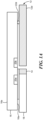
- Transducer/coil pair 20a includes an electromagnetic shield 46 disposed between the current conductor 18 and the first surface 16a of the substrate 16 on which the coils 40a, 40b are disposed in order to prevent unwanted capacitive coupling from the conductor 18 to the sensing elements 38a, 38b, 40a, 40b.
- a capacitively-coupled signal represents a change in the voltage potential of the lead frame 12. In some applications in which current sensor 10 can be used, such as with motor control or DC/DC converters, this voltage can change rapidly and not in response to a change in the current through conductor 18.
- the shield 46 is shown on a "metal 3" layer that is coupled to a reference potential (i.e., ground) to prevent capacitive coupling from the lead frame 12 to the sensing elements. Since the substrate 16 is packaged in a flip-chip configuration, the conductor 18 is closest to the top level of metal (the metal 3 shield layer 46).
- Coil 40a is on “metal 1" and “metal 2" layers, as shown.
- a cross-under trace 44 is provided on a different metal layer in order to interconnect two portions of the coil 40a, as shown.
- a second shield 48 is provided on the other side of the coil 40a from shield 46 in order to prevent unwanted capacitive coupling from the current conductor 18 of the lead frame 12 into the substrate 16.
- shield 46 is on metal layer 4
- coil 40a is on metal layers 2 and 3
- second shield 48 is on metal layer 1.
- any change in the metal resistance results in an undesired change in the gain of the sensor.
- electromagnetic shield 46 may take the form of a substantially planar layer and includes at least one feature selected to reduce an eddy current induced in the shield by reducing a path length of a closed loop current path in the shield. Such is desirable since eddy currents would result in a decrease in bandwidth.
- shield 46 may comprise a metal layer with a generally serpentine pattern arranged in four quadrants with elongated slots 46a - 46d between the quadrants. It will be appreciated by those of ordinary skill in the art that other shield designs and eddy current reduction features are possible. Further, it will be appreciated that shield layers 46, 48 can be the same as each other or different.
- current sensor 10 can be provided in the form of an integrated circuit (IC) in which the elements of FIG. 1 are over molded with a nonconductive material to form packaged IC 50, as shown.
- IC integrated circuit
- Various molding techniques are possible, including but not limited to injection molding, compression molding, transfer molding, and/or potting, with various materials suitable to electrically isolate and mechanically protect the device.
- Suitable materials for the mold material include thermoset and thermoplastic mold compounds and other commercially available IC mold compounds.
- Leads 12a - 12f have ends formed for surface mount attachment to a printed circuit board and/or bus bar or other supporting substate or structure in use. It will be appreciated by those of ordinary skill in the art however that other attachment structures and techniques are possible for electrically coupling the current sensor 10 to external circuits and systems.
- FIG. 2 a simplified schematic block diagram of the current sensor 10 is shown to include transducer/coil pairs 20a, 20b, with each pair pictorially shown positioned on opposite sides of current conductor 18.
- the dotted line box around sensor 10 represents the integrated circuit package 50 ( FIG. 1E ), with leads 12a - 12f illustrated by connection points to/from the IC.
- the signal leads 12c - 12f are arbitrarily assigned to the various electrical connections and can be varied and/or more or fewer signal lead and other connections can be provided.
- transducer/coil pair 20a includes Hall effect element 38a and coil 40a and transducer/coil pair 20b includes Hall effect element 38b and coil 40b.
- Transducer 38a is configured to generate a first magnetic field signal and transducer 38b is configured to generate a second magnetic field signal.
- Coil 40a is configured to generate a third magnetic field signal and coil 40b is configured to generate a fourth magnetic field signal.
- Sensor 10 includes a first signal path 50 coupled to receive the magnetic field signals from transducers 38a, 38b and configured to generate a low frequency signal 54 associated with a low frequency content of the current 28 ( FIG.
- a cross-over network as may include summation circuit 58 is configured to sum the low frequency signal 54 and the high frequency signal 56 to provide a wide bandwidth signal 68 indicative of the current through the conductor 18.
- the first and second Hall effect elements 38a, 38b detect the magnetic field generated by the current 28 in opposite directions since the elements are positioned on opposite sides of the conductor portion 14.
- the coils 40a, 40b detect the magnetic field generated by the current 28 in opposite directions since the coils are on opposite sides of the conductor portion 14.
- Signal path 50 generates the low frequency signal 54 from a differential signal generated by subtraction of the magnetic field signal from transducer 38b from the magnetic field signal from transducer 38a by operation of amplifier 70.
- signal path 52 generates the high frequency signal 56 from a differential signal generated by subtraction of the magnetic field signal from coil 40b from the magnetic field signal from coil 40a by operation of integrator 80.
- the low frequency signal path 50 can include dynamic offset cancellation circuitry 64 to remove offset that can be associated with the magnetic field sensing elements 38a, 38b and/or the amplifier 70.
- Dynamic offset cancellation circuitry 64 may include chopping circuitry with switches configurable to drive the magnetic field sensing elements 38a, 38b in two or more different directions such that selected drive and signal contact pairs are interchanged during each phase of a chopping clock signal and offset voltages of the different driving arrangements tend to cancel.
- Front-end amplifier 70 is coupled to receive offset adjusted signals from sensing elements 38a, 38b and can be responsive to a sensitivity control circuit 72 to generate an amplified signal.
- Sensitivity control circuit 72 can generate and provide a sensitivity control signal to the amplifier 70 to adjust a sensitivity and/or operating voltage of the amplifier.
- a notch filter and dV/dt rejection circuit 76 can be coupled to receive the amplified signal and generate an impulse filtered signal.
- Low pass filter 78 can operate on the impulse filtered signal to generate the low frequency signal 54. Suffice it to say here that since the low frequency signal path has a relatively low bandwidth, an impulse disturbance can take a long time to dissipate.
- Use of the dV/dt rejection circuit 76 can advantageously remove impulse disturbances that are not eliminated by the shield 46 ( FIGs. 1D ). Details of an example dV/dt filter are discussed below in connection with FIG. 5 .
- the high frequency signal path 52 can include an integrator and offset rejection circuit 80 coupled to receive the magnetic field signals from coils 40a, 40b.
- the integrator portion of circuit 80 is configured to maintain a substantially flat frequency response and the offset rejection portion of circuit 80 is configured to prevent saturation of the coil path 52 from offset amplified by the integrator.
- a graph 200 illustrates gain associated with the high frequency path 52, with a horizontal axis representing frequency in arbitrary units of Hertz and a vertical axis representing gain in arbitrary units of decibels.
- Curve 204 illustrates an example gain associated with coils 40a, 40b. Since coils 40a, 40b are inductively coupled to detect the magnetic field generated by the current through conductor 18, the signal strength increases with increasing frequency, as may occur at an example rate of approximately 20dB/dec.
- the signals from coils 40a, 40b are passed through an integrator 80.
- the gain of the integrator 80 is illustrated by curve 208.
- Integrator 80 is designed to attenuate the signal at the same rate as the coil gain increases over frequency (e.g., at a rate of 20 dB/dec), resulting in a substantially flat gain curve 210 representing combined gain of the coils and integrator.
- An amplifier 84 can be coupled to a sensitivity control circuit 86 that can be the same as or similar to sensitivity control circuit 72.
- a high pass filter 88 can be coupled to receive the amplified signal and configured to generate the high frequency signal 56.
- integrator 80 Since integrator 80 provides a high gain at DC, any input offset of the integrator is amplified. In order to prevent the saturation of the coil path 52 from this amplified offset, compensation is implemented by circuit 80 as will be explained further in connection with FIGs. 3 - 3D .
- the output signal of summation circuit 58 can be amplified by an amplifier 60 with further offset control by an offset control circuit 62 in order to generate the current sensor output signal 68 indicative of wide frequency band of current through conductor 18.
- Additional components of current sensor 10 can include a digital system 100 containing various signal processing elements, such as an EEPROM and control logic block 104.
- EEPROM and control logic block 104 determines any application-specific coding and can be erased and reprogrammed using a pulsed voltage.
- An active temperature compensation circuit 108 can be coupled to acquire temperature data from a temperature sensor 110 and can perform calculations to compensate for changes in temperature.
- Current sensor 10 can include fault detection circuitry to detect various faults and provide a FAULT output signal.
- fault detection circuitry can detect an overcurrent condition and/or an undercurrent condition indicating that the current through conductor 18 is greater than or less than respective thresholds, respectively.
- a comparator 120 can be coupled to receive the current sensor output signal 68 and one or more threshold levels from a fault setting block 124.
- An output of comparator 120 can be coupled to a fault delay logic circuit 128 and provide a FAULT signal at an output (e.g., at signal lead 12d) via one or more drivers 130.
- Fault delay logic 128 can be used to process the comparator output in various ways.
- An output of the current sensor at lead 12d can be a dual-purpose output at which fault detection information or a reference voltage VREF is provided by operation of complementarily controlled switches 132a, 132b.
- Reference voltage VREF can be provided by a bandgap reference 138 with amplification and offset control provided by elements 140, 142, respectively.
- a programming control block 146 can be used to control switches 132a, 132b.
- a power lead 12c can be coupled to receive a supply voltage VCC for a voltage regulator 148 to generate one or more regulated voltages to power the various components and sub-circuits of the sensor 10.
- a ground lead 12f can be configured to couple to a reference or ground potential.
- example current sensor 10 has an analog front-end portion and a digital portion, it will be appreciated that the particular delineation of which circuit functions are implemented in an analog fashion or with digital circuitry and signals can be varied. Some of the illustrated circuit functions can be implemented on an integrated circuit sensor 10 and other circuitry and functionality can be implemented on separate circuits (e.g., additional substrates within the same integrated circuit package, or additional integrated circuit packages, and/or on circuit boards).
- conductor 18 and coils 40a, 40b are shown coupled to integrator and offset rejection circuit 80, here shown to include integrator 304 and an offset rejection circuit in the form of a Proportional-Integral (PI) feedback circuit 302.
- integrator and offset rejection circuit 80 here shown to include integrator 304 and an offset rejection circuit in the form of a Proportional-Integral (PI) feedback circuit 302.
- PI Proportional-Integral
- Each coil 40a, 40b has a first terminal coupled to integrator 304 and a second terminal coupled to the other one of the coils at a common mode voltage node VCM 300. Stated differently, of the four coil connections, two go to the common mode voltage node VCM and the remaining two go to the integrator resistors, as shown.
- Coils 40a, 40b can be wound in the same direction. With this configuration, in operation, coil output signals from stray magnetic fields will be subtracted out because, even though the coils are positioned on opposite sides of the conductor 18, stray fields will impact both coils in same fashion (in terms of field magnitude and polarity) so that subtraction of one coil signal from the other will negate the impact of the stray field. In this way, placement of the two coils 40a, 40b on different sides of the conductor provides immunity to stray fields.
- the magnetic signal generated by the current in conductor 18 can cause a current to flow into the common mode voltage reference VCM 300. If the coupling from lead frame 12 were matched to each coil 40a and 40b, then the amplitude of the coil voltages would match. With matched resistors 312 and 316, each of which are connected to a "virtual VCM" at the inputs to amplifier 308, the current flowing through the coils 40a and 40b and resistor 312 and 316 are equal. In this case, the voltage reference driving VCM does not need to supply any current.
- Integrator 304 includes a differential amplifier 308 having an inverting input 308a to which resistors 310, 312 are coupled and a non-inverting input 308b to which resistors 316, 318 are coupled, as shown.
- Each input 308a, 308b acts as a summing node.
- Each of differential outputs 308c, 308d of the amplifier 308 is coupled in a feedback relationship to a respective input 308a, 308b by a respective feedback capacitor 320, 322, as shown.
- the differential output signal 82 of circuit 80 is provided at amplifier outputs 308c, 308d.
- the example integrator 304 advantageously permits a convenient method for the summation of the feedback signals and input signals from the coils. However, it will be appreciated by those of ordinary skill in the art other integrator implementations, such as a transconductor and load capacitor, are also possible.
- the PI circuit 302 is coupled in a feedback relationship with the integrator 304. To this end, PI circuit 302 is coupled to receive differential signal 82 and provide input signals coupled to integrator inputs through resistors 310 and 318, as shown. Although the PI circuit 302 could be implemented either with external or with internal (i.e., "on-chip") components, it can be advantageous to integrate circuit 302 within the sensor IC for cost and space reasons.
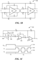
- a simplified PI circuit 330 as may provide the PI circuit 302 of FIG. 3 contains a proportional path 334 and an integral path 336, which paths are combined by a summation element 348.
- the proportional path 334 can include a proportional gain Kp 340 and the integral path 336 can include an integrating stage 342 and integral constant Ki 344.
- an example PI circuit 350 as may provide the PI circuit 302 of FIG. 3 can include an integral stage including an operational amplifier 352 and a proportional stage including an operational amplifier 354.
- the integral stage includes feedback capacitors C and input resistors R 0 coupled to the differential inputs of amplifier 352, as shown.
- the differential output of amplifier 352 is cross-coupled to inputs of proportional stage amplifier 354 in order to thereby introduce a signal inversion.
- Proportional amplifier 354 has feedback resistors R 2 and input resistors R 3 as shown.
- the PI feedback cancels the integrator amplifier offset by storing charge on capacitors C that creates a voltage (scaled by R 2 R 3 ) that equals the offset. When subtracted at the integrator input, the offset is eliminated.
- a time constant of the PI circuit 350 is established by a capacitance of the feedback capacitors C and an effective resistance of the input resistors R 0 .
- the two-amplifier network implementing the PI feedback circuit 350 uses the gain to effectively increase the component values, creating similar time constants on-chip without the need for large components that could require off-chip implementation. More particularly, the pole shown in the integrator curve 208 ( FIG. 2A ) is attributable to the time constant given by R 2 /sCR 0 R 3 . This pole needs to be low enough so that it does not alter the frequency response of the high frequency coil path. Implementing this time constant with a single RC would require a value of capacitance that is too large to be implemented on an integrated circuit. By adding the R 2 /R 3 gain factor, the capacitance value C can be reduced to a size that enables on-chip components to be used.
- the purpose of the PI circuit is to minimize low frequency gain of the coil front end, and it accomplishes this by feeding back low frequency signals to the input where they are subtracted from the incoming signals from the coil. This minimizes the amplitude of amplifier offset at the integrator output, but also minimizes low frequency signals from the coil.
- To allow the desired high frequency signals from the coil to pass necessitates a long time constant in the PI feedback so that it does respond to those signals. Upon power-up of the sensor 10, this means a relatively long time for the charge to accumulate on capacitors C. This time constant can be adjusted by changing the value of R 0 .
- an alternative PI circuit 360 as may provide the PI circuit 302 of FIG. 3 includes a switched capacitor circuit 372 in series with input resistor R 0 .
- the input resistor R 0 of FIG. 3B is replaced in the PI circuit 380 of FIG. 3C by a combination of a fixed resistor R 0 and switched capacitor network 372.
- PI circuit 360 further differs from the PI circuit 350 of FIG. 3B in that it illustrates a single-ended PI circuit implementation with the signal inversion (achieved in FIG. 3B by the cross-coupling of the differential outputs of amplifier 352) illustrated by a negative resistance - R 3 .
- PI circuit 360 can be similar to PI circuit 350 and can include an integral stage including an operational amplifier 362 and a feedback capacitor C and a proportional stage including an operational amplifier 364.
- Proportional amplifier 364 has a feedback resistor R 2 and an input resistor -R 3 , as shown.
- Switched capacitor network 372 includes a plurality of switches 366, 368, 370 and a capacitor C R that operate to change the value of the input resistance to the integrating operational amplifier 362. Switches 366, 368, and 370 are controlled by control signals ⁇ 1 376, ⁇ 2 378, and ⁇ start 374, respectively.
- switch 370 In operation, during a startup period (during a time labeled T1), when it is desired to quickly charge capacitor C, switch 370 is closed by control signal ⁇ start 374, thereby reducing the time needed to develop an equivalent offset voltage on capacitor C. Following the startup period (during a time labeled T2), when it is desired to have a lower corner frequency through the integrator path, switch 370 is opened by control signal ⁇ start 374 and switches 366, 368 are selectively opened and closed in a complementary manner by respective control signals 376, 378 in order to thereby increase the effective value of the input resistance to the operational amplifier 362. With this arrangement, the PI circuit 360 has a fast startup, and a better low frequency response during normal operation.
- PI circuit 360 can be implemented using only on-chip components and does not require zero/pole matching for its operation.
- the placement of the zero is determined by resistors R 0 , R 2 , and R 3 and capacitor C and this design is tolerant to movement of the zero with normal process variations for resistors and capacitors.
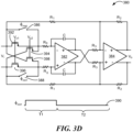
- a further alternative PI circuit 380 as may provide the PI circuit 302 of FIG. 3 includes a MOSFET-C approach to providing a fast startup with better low frequency response during normal operation.
- the input resistor R 0 of FIG. 3B is replaced in the PI circuit 380 of FIG. 3D by a combination of a fixed resistors R 0 and MOSFET-C circuitry including FETs 392, 394, 396, 398 and switches 386 and 388 coupled as shown.
- PI circuit 380 can be a differential circuit as shown and includes an integral stage including an operational amplifier 382 and feedback capacitors C and a proportional stage including an operational amplifier 384.
- Proportional amplifier 384 has a feedback resistors R 2 and input resistors R 3 , as shown.
- FETs 392, 394, 396, 398 and switches 386 and 388 operate to implement a tunable resistance without the need for clock circuitry.
- the PI circuit 380 does not require anti-aliasing circuitry or clock signals.
- FETs 392 and 396 are controlled by a gate voltage V c1 and FETs 394, 398 are controlled by a gate voltage V c2 , which gate voltages can be preset or adjustable in order to achieve a desired effective resistance.
- Switches 386, 388 are controlled by control signal ⁇ start 390.
- switches 386, 388 are closed by control signal ⁇ start 390, thereby effectively shorting FETs 392, 394, 396, and 398.
- the input resistance to amplifier 382 is based only on the resistance of resistors R 0 thereby minimizing the time needed to develop an equivalent offset voltage on capacitors C.
- switches 386, 388 are opened by control signal ⁇ start 390.
- the effective input resistance at the inverting input terminal to amplifier 382 is provided by the series combination of resistor R 0 with a parallel combination of FETs 392 and 398 and the effective input resistance at the non-inverting input to amplifier 382 is provided by the series combination of resistor R 0 with a parallel combination of FETs 394 and 396.
- the PI circuit 380 has a fast startup, and a better low frequency response during normal operation.
- an equivalent circuit 400 illustrates coils 40a, 40b and conductor 18.
- conductor 18 is represented by a primary inductance Lp and a series primary resistance Rp.
- Each of coils 40a, 40b is represented by a respective inductance Lr, and series resistance Rr, and stray capacitance Cr, as shown.
- a common mode voltage reference, VCM drives the node between the series resistance and stray capacitance associated with the coils, as shown.
- An output voltage Vout represents a series summation of the signals from the coils 40a, 40b.
- a stray magnetic field on the coils 40a, 40b will be subtracted out in the output voltage Vout because the coils are exposed to the same magnetic field, thus creating identical voltages at their output terminals. While both output terminals will move magnetic field, they are connected to opposite inputs of a differential amplifier which has common mode feedback circuitry to remove the common mode signal.
- coils 440a, 440b are formed in a "figure eight" pattern to minimize the common mode voltage variation.
- Coils 440a, 440b can be used in place of coils 40a, 40b and thus are shown coupled to integrator 304 ( FIG. 3 ).
- Each coil 440a, 440b is made up of two coils wound in opposite directions, with one such coil coupled to the inverting input 308a of the operational amplifier 308 and the other such coil coupled to the non-inverting input 308b of the operational amplifier 308.
- coils 440a, 440b are made up of four coils and, of the eight connections to these four coils, four connections go to the common mode node VCM and four go to integrator resistors 310, 312, 316, 318.
- coil 440a includes coils 444a and 448a which coils are wound in opposite directions with respect to each other and coil 440b includes coils 444b and 448b which coils are wound in opposite directions with respect to each other.
- coil 444a is wound in a counterclockwise direction and coil 448a is wound in a clockwise direction, with coil 444a coupled to the non-inverting input 308b of operational amplifier 308 and coil 448b coupled to the inverting input 308a of operational amplifier 308.
- Coil 444b is wound in a clockwise direction and coil 448b is wound in a counterclockwise direction, with coil 444b coupled to the non-inverting input 308b of operational amplifier 308 and coil 448b coupled to the inverting input 308a of operational amplifier 308, as shown.
- each of the coils 440a, 440b is split into two coils 444a, 448a and 444b, 448b that are wound in opposite directions with respect to each other and coupled to operational amplifier inputs of opposite polarity resulting in these signals of opposite polarity adding at the integrator input summing nodes.
- the mismatch in the coupling to the inside of the loop 14 coils and the outside of the loop 14 coils is corrected by creating an equal voltage signal to both of the inverting input 308a and non-inverting input 308b. This reduces the need for the reference VCM and the common-mode feedback of the operational amplifier 308 to correct for the mismatch.
- coils 444a, 444b are shown offset from each other and coils 448a, 448b are shown offset from each other in the perspective pictorial representation of FIG. 4A , in practice, turns of these coils can be vertically aligned.
- Coils 440a, 440b with their respective constituent coils 444a, 448a and 444b, 448b can be constructed from multiple metal layers if the process has more the four levels of metal.
- the shield 46 FIG. 1D
- the shield 46 could be on metal layer 6, coils 444a, 444b on metal layers 4 and 5, and coils 448a, 448b on metals 2 and 3.
- the illustrated configuration of coils 440a, 440b can reduce variation of the common mode voltage. This simplifies the common mode rejection requirements for the front end for a given magnetic field magnitude and frequency.
- an example dV/dt filter 500 as can be used in the notch filter and dV/dt rejection circuit 76 of FIG. 2 includes a plurality of delay devices 522a-522n and filter 550.
- Filter 550 can be configured to reduce or eliminate errors due to voltage transients.
- the output of amplifier 70 FIG. 2
- the output of amplifier 70 can be sampled and a current sample can be provided to first delay device 522a, which delay device 522a provides the previous sample to a second delay device 522b and each successive previous sample can be provided to delay devices 522c-522n respectively, as shown.
- An output of each of delay devices 522a-522n (that can be the same output that is provided to a subsequent delay device 522b-522n) can be provided to a respective input of filter 550.
- filter 550 can be configured to generate a median sample based on each of the samples received.
- Filter 550 can store multiple samples and generate the median sample value of the multiple samples to ignore a voltage transient event.
- filter 550 can store an odd number of at least three previous samples and compute a median value of the stored previous samples.
- filter 550 can store three or more odd number of samples and the median sample can be based on those samples.
- the three samples may be used to limit the effect of a single voltage transient event within the three samples.
- other numbers of samples may be used to generate the median sample value.
- Filter 550 can provide the median sample, or the median value of the stored previous samples as an output signal to low pass filter 78 ( FIG. 2 ).
Landscapes
- Physics & Mathematics (AREA)
- General Physics & Mathematics (AREA)
- Engineering & Computer Science (AREA)
- Power Engineering (AREA)
- Measuring Instrument Details And Bridges, And Automatic Balancing Devices (AREA)
Claims (19)
- Stromsensor, umfassend:einen Leiterrahmen (12), der eine Vielzahl von Leitungen (12a-12f) aufweist, wobei zumindest zwei der Vielzahl von Leitungen (12a-12f) einen Stromleiter (18) bilden, der zum Führen eines Stroms ausgelegt ist, der ein Magnetfeld erzeugt;ein Substrat (16), aufweisend eine erste und eine zweite gegenüberliegende Oberfläche (16a, 16b), wobei die erste Oberfläche (16a) proximal zu dem Stromleiter (18) und die zweite Oberfläche (16b) distal von dem Stromleiter liegt;einen auf dem Substrat (16) angeordneten ersten Magnetfeldwandler (20a);eine auf dem Substrat angrenzend an den ersten Magnetfeldwandler angeordnete erste Spule (440a), wobei der erste Magnetfeldwandler und die erste Spule (440a) auf einer ersten Seite des Stromleiters (18) angeordnet sind;einen auf dem Substrat (16) angeordneten zweiten Magnetfeldwandler (20b); undeine auf dem Substrat angrenzend an den zweiten Magnetfeldwandler angeordnete zweite Spule (440b), wobei der zweite Magnetfeldwandler und die zweite Spule (440b) auf einer zweiten Seite des Stromleiters (18) angeordnet sind,dadurch gekennzeichnet, dass die erste Spule (440a) dritte und vierte Spulen (444a, 448a) umfasst, die in entgegengesetzten Richtungen zueinander gewickelt sind, und die zweite Spule (440b) fünfte und sechste Spulen (444b, 448b) umfasst, die in entgegengesetzten Richtungen zueinander gewickelt sind.
- Stromsensor nach Anspruch 1, wobei der Stromleiter gebogen ist und wobei die erste Seite des Stromleiters innerhalb der Biegung liegt und wobei die zweite Seite des Stromleiters außerhalb der Biegung liegt.
- Stromsensor nach Anspruch 1, wobei die erste Spule konzentrisch in Bezug auf den ersten Magnetfeldwandler angeordnet ist und die zweite Spule konzentrisch in Bezug auf den zweiten Magnetfeldwandler angeordnet ist.
- Stromsensor nach Anspruch 1, wobei der erste Magnetfeldwandler und der zweite Magnetfeldwandler auf der ersten Oberfläche des Substrats angeordnet sind.
- Stromsensor nach Anspruch 1, ferner umfassend eine zwischen dem Stromleiter und der ersten und zweiten Spule angeordnete Abschirmung (46), wobei die Abschirmung zumindest ein Merkmal aufweist, das zum Reduzieren eines in der Abschirmung induzierten Wirbelstroms ausgewählt wurde.
- Stromsensor nach Anspruch 5, wobei die Abschirmung zumindest einen zum Reduzieren der Weglänge einer geschlossenen Stromschleife in der Abschirmung ausgelegten Schlitz (46a-46d) umfasst.
- Stromsensor nach Anspruch 5, wobei die Abschirmung eine erste Abschirmung (46) umfasst und wobei der Stromsensor ferner eine zweite Abschirmung (48) umfasst, die zwischen der ersten und zweiten Spule und der zweiten Oberfläche des Substrats angeordnet ist.
- Stromsensor nach Anspruch 1, wobei der erste Magnetfeldwandler und der zweite Magnetfeldwandler jeweils ein Halleffekt-Element umfassen.
- Stromsensor nach Anspruch 1, wobei der erste Magnetfeldwandler zum Erzeugen eines ersten Magnetfeldsignals ausgelegt ist, der zweite Magnetfeldwandler zum Erzeugen eines zweiten Magnetfeldsignals ausgelegt ist, die erste Spule zum Erzeugen eines dritten Magnetfeldsignals ausgelegt ist und die zweite Spule zum Erzeugen eines vierten Magnetfeldsignals ausgelegt ist, und wobei der Stromsensor ferner umfasst:einen zum Empfangen des ersten und zweiten Magnetfeldsignals gekoppelten und zum Erzeugen eines mit einem Niederfrequenzinhalt des Stroms durch den Stromleiter verbundenen Niederfrequenzsignals ausgelegten ersten Signalpfad (50);einen zum Empfangen des dritten und vierten Magnetfeldsignals gekoppelten und zum Erzeugen eines mit einem Hochfrequenzinhalt des Stroms durch den Stromleiter verbundenen Hochfrequenzsignals ausgelegten zweiten Signalpfad (52); undeine zum Summieren des Niederfrequenzsignals und des Hochfrequenzsignals zum Bereitstellen eines den Strom durch den Stromleiter anzeigenden Signals ausgelegte Summierschaltung (58).
- Stromsensor nach Anspruch 9, wobei der erste Magnetfeldwandler und der zweite Magnetfeldwandler das Magnetfeld in entgegengesetzten Richtungen erfassen, wobei die erste Spule und die zweite Spule das Magnetfeld in entgegengesetzten Richtungen erfassen, wobei das Niederfrequenzsignal ein Differenzsignal ist, das durch Subtraktion des zweiten Magnetfeldsignals von dem ersten Magnetfeldsignal erzeugt wird, und wobei das Hochfrequenzsignal ein Differenzsignal ist, das durch Subtraktion des vierten Magnetfeldsignals von dem dritten Magnetfeldsignal erzeugt wird.
- Stromsensor nach Anspruch 9, wobei der erste Signalpfad umfasst:einen dV/dt-Filter (76), der auf die ersten und zweiten Magnetfeldsignale reagiert und zum Erzeugen eines impulsgefilterten Signals ausgelegt ist; undeinen Tiefpassfilter (78), der zum Empfangen des impulsgefilterten Signals gekoppelt und zum Erzeugen des Niederfrequenzsignals ausgelegt ist.
- Stromsensor nach Anspruch 11, wobei der dV/dt-Filter einen Medianfilter umfasst.
- Stromsensor nach Anspruch 9, wobei der zweite Signalpfad umfasst:einen zum Empfangen des dritten und vierten Magnetfeldsignals gekoppelten und einen Verstärker umfassenden Integrator (80); undeinen Offset-Sperrkreis (80), der in einer Rückkopplungsbeziehung zwischen einem Ausgang und einem Eingang des Verstärkers gekoppelt ist, wobei der Offset-Sperrkreis eine proportionale Integralschaltung (302) umfasst, die zum Kompensieren eines Offsets des Verstärkers ausgelegt ist.
- Stromsensor nach Anspruch 13, wobei die Proportional-Integral-Schaltung umfasst:eine Integratorstufe, umfassend einen Integrationsverstärker mit einem Rückkopplungskondensator und einem ersten Eingangswiderstand; undeine Proportionalstufe, umfassend einen Verstärker mit einem zweiten Eingangswiderstand und einem Rückkopplungswiderstand, wobei eine Verstärkung des Integrators durch eine Kapazität des Rückkopplungskondensators und einen effektiven Widerstand des ersten Eingangswiderstands, des zweiten Eingangswiderstands und des Rückkopplungswiderstands festgelegt wird.
- Stromsensor nach Anspruch 14, wobei der erste Eingangswiderstand einen Festwiderstand und eine geschaltete Kondensatorschaltung mit einer Vielzahl von Schaltern und einem Kondensator umfasst.
- Stromsensor nach Anspruch 15, wobei die Vielzahl von Schaltern der geschalteten Kondensatorschaltung während einer Startperiode gesteuert wird, um den effektiven Widerstand des ersten Eingangswiderstands zu verringern, um dadurch die Zeitkonstante des Integrators zu verringern, und wobei die Vielzahl von Schaltern der geschalteten Kondensatorschaltung nach der Startperiode gesteuert wird, um den effektiven Widerstand des ersten Eingangswiderstands zu erhöhen, um dadurch die Zeitkonstante des Integrators zu erhöhen.
- Stromsensor nach Anspruch 1, ferner umfassend ein Gehäuse für eine integrierte Schaltung, das zum Umschließen des Substrats und zumindest eines Teils der Vielzahl von Leitungen des Leiterrahmens ausgelegt ist.
- Stromsensor nach Anspruch 14, wobei der erste Eingangswiderstand einen Festwiderstand und eine MOSFET-C-Schaltung umfasst, die eine Vielzahl von MOSFETs und einen oder mehrere parallel zu der Vielzahl von MOSFETs geschaltete Schalter umfasst.
- Stromsensor nach Anspruch 16, wobei der eine oder die mehreren Schalter der MOSFET-C-Schaltung während einer Startperiode gesteuert werden, um den effektiven Widerstand des ersten Eingangswiderstands zu verringern, um dadurch die Zeitkonstante des Integrators zu verringern, und wobei der eine oder die mehreren Schalter der MOSFET-C-Schaltung nach der Startperiode gesteuert werden, um den effektiven Widerstand des ersten Eingangswiderstands zu erhöhen, um dadurch die Zeitkonstante des Integrators zu erhöhen.
Priority Applications (1)
| Application Number | Priority Date | Filing Date | Title |
|---|---|---|---|
| EP24180408.7A EP4459294A3 (de) | 2021-01-28 | 2021-12-10 | Mehrwegstromsensor mit grosser bandbreite |
Applications Claiming Priority (1)
| Application Number | Priority Date | Filing Date | Title |
|---|---|---|---|
| US17/160,573 US11366141B1 (en) | 2021-01-28 | 2021-01-28 | Multipath wide bandwidth current sensor |
Related Child Applications (2)
| Application Number | Title | Priority Date | Filing Date |
|---|---|---|---|
| EP24180408.7A Division EP4459294A3 (de) | 2021-01-28 | 2021-12-10 | Mehrwegstromsensor mit grosser bandbreite |
| EP24180408.7A Division-Into EP4459294A3 (de) | 2021-01-28 | 2021-12-10 | Mehrwegstromsensor mit grosser bandbreite |
Publications (3)
| Publication Number | Publication Date |
|---|---|
| EP4036587A1 EP4036587A1 (de) | 2022-08-03 |
| EP4036587B1 true EP4036587B1 (de) | 2024-08-07 |
| EP4036587C0 EP4036587C0 (de) | 2024-08-07 |
Family
ID=78829589
Family Applications (2)
| Application Number | Title | Priority Date | Filing Date |
|---|---|---|---|
| EP24180408.7A Pending EP4459294A3 (de) | 2021-01-28 | 2021-12-10 | Mehrwegstromsensor mit grosser bandbreite |
| EP21213675.8A Active EP4036587B1 (de) | 2021-01-28 | 2021-12-10 | Multipfad-breitband-stromsensor |
Family Applications Before (1)
| Application Number | Title | Priority Date | Filing Date |
|---|---|---|---|
| EP24180408.7A Pending EP4459294A3 (de) | 2021-01-28 | 2021-12-10 | Mehrwegstromsensor mit grosser bandbreite |
Country Status (2)
| Country | Link |
|---|---|
| US (1) | US11366141B1 (de) |
| EP (2) | EP4459294A3 (de) |
Families Citing this family (12)
| Publication number | Priority date | Publication date | Assignee | Title |
|---|---|---|---|---|
| KR102875948B1 (ko) * | 2021-08-06 | 2025-10-24 | 현대모비스 주식회사 | 노이즈 영향 저감형 로고스키 센서와 그 제조방법 그리고 신호처리 회로 |
| JP7614992B2 (ja) * | 2021-09-16 | 2025-01-16 | 株式会社東芝 | 電流検出装置 |
| US11994541B2 (en) | 2022-04-15 | 2024-05-28 | Allegro Microsystems, Llc | Current sensor assemblies for low currents |
| US12140646B2 (en) | 2023-02-06 | 2024-11-12 | Allegro Microsystems, Llc | Magnetic sensing having hall plate routing to reduce inductive coupling |
| CN115902380B (zh) * | 2023-03-08 | 2023-06-16 | 保定天威新域科技发展有限公司 | 一种超宽带电流智能传感器 |
| US12578176B2 (en) | 2023-03-22 | 2026-03-17 | Allegro Microsystems, Llc | Angle sensor using eddy currents and having harmonic compensation |
| JP2024146826A (ja) * | 2023-03-31 | 2024-10-15 | 旭化成エレクトロニクス株式会社 | 電流測定モジュール |
| US12510611B2 (en) | 2023-11-07 | 2025-12-30 | Allegro Microsystems, Llc | TMR sensor having magnetic field generation for pillar stimulation |
| US12613293B2 (en) | 2023-12-04 | 2026-04-28 | Allegro Microsystems, Llc | Sensor with common mode rejection and offset correction |
| CN120446567A (zh) * | 2024-02-07 | 2025-08-08 | 台达电子工业股份有限公司 | 多路径的电流差检测装置 |
| US20250334612A1 (en) * | 2024-04-30 | 2025-10-30 | Allegro Microsystems, Llc | Substrate-embedded ac sensors |
| WO2026022254A1 (en) * | 2024-07-23 | 2026-01-29 | Systematic Design B.V. | Magnetic current sensing |
Family Cites Families (10)
| Publication number | Priority date | Publication date | Assignee | Title |
|---|---|---|---|---|
| US20060219436A1 (en) * | 2003-08-26 | 2006-10-05 | Taylor William P | Current sensor |
| US7768083B2 (en) | 2006-01-20 | 2010-08-03 | Allegro Microsystems, Inc. | Arrangements for an integrated sensor |
| US10145908B2 (en) | 2013-07-19 | 2018-12-04 | Allegro Microsystems, Llc | Method and apparatus for magnetic sensor producing a changing magnetic field |
| US10352969B2 (en) | 2016-11-29 | 2019-07-16 | Allegro Microsystems, Llc | Systems and methods for integrated shielding in a current sensor |
| US10156614B2 (en) * | 2016-11-29 | 2018-12-18 | Allegro Microsystems, Llc | Systems and methods for sensing a voltage transient in a magnetic field sensor integrated circuit |
| US10641802B2 (en) * | 2018-03-22 | 2020-05-05 | Allegro Microsystems, Llc | Current fault detection systems and methods for a current sensor |
| DE102018111011A1 (de) * | 2018-05-08 | 2019-11-14 | Infineon Technologies Ag | Magnetfeldsensorvorrichtung |
| US10935612B2 (en) | 2018-08-20 | 2021-03-02 | Allegro Microsystems, Llc | Current sensor having multiple sensitivity ranges |
| US11800813B2 (en) * | 2020-05-29 | 2023-10-24 | Allegro Microsystems, Llc | High isolation current sensor |
| US11519941B2 (en) * | 2020-07-27 | 2022-12-06 | Analog Devices International Unlimited Company | Current sensing device having an integrated electrical shield |
-
2021
- 2021-01-28 US US17/160,573 patent/US11366141B1/en active Active
- 2021-12-10 EP EP24180408.7A patent/EP4459294A3/de active Pending
- 2021-12-10 EP EP21213675.8A patent/EP4036587B1/de active Active
Also Published As
| Publication number | Publication date |
|---|---|
| EP4459294A3 (de) | 2025-01-08 |
| EP4036587A1 (de) | 2022-08-03 |
| EP4459294A2 (de) | 2024-11-06 |
| US11366141B1 (en) | 2022-06-21 |
| EP4036587C0 (de) | 2024-08-07 |
Similar Documents
| Publication | Publication Date | Title |
|---|---|---|
| US11366141B1 (en) | Multipath wide bandwidth current sensor | |
| US7259545B2 (en) | Integrated sensor | |
| US10114044B2 (en) | Current sensor | |
| EP2609442B1 (de) | Vorrichtung und verfahren zur reduzierung eines transienten signals bei einem magnetfeldsensor | |
| US8080994B2 (en) | Integrated current sensor | |
| US9958482B1 (en) | Systems and methods for a high isolation current sensor | |
| US10247758B2 (en) | Current sensor | |
| EP1965217B1 (de) | Stromsensor mit offenem Regelkreis und hoher Bandbreite | |
| US7642768B1 (en) | Current sensor having field screening arrangement including electrical conductors sandwiching magnetic permeability layer | |
| US11892476B2 (en) | Current sensor package | |
| US20210033646A1 (en) | Multi-Die Integrated Current Sensor | |
| EP4443182B1 (de) | Strommesssystem | |
| US11879951B2 (en) | Magnetic field sensor apparatus | |
| US12078662B2 (en) | Techniques for reducing an eddy current in a ground plane of a coreless sensor | |
| US12282075B2 (en) | Sensor package and system | |
| US11408945B2 (en) | Magnetic field sensor with stacked transducers and capacitive summing amplifier |
Legal Events
| Date | Code | Title | Description |
|---|---|---|---|
| PUAI | Public reference made under article 153(3) epc to a published international application that has entered the european phase |
Free format text: ORIGINAL CODE: 0009012 |
|
| STAA | Information on the status of an ep patent application or granted ep patent |
Free format text: STATUS: THE APPLICATION HAS BEEN PUBLISHED |
|
| AK | Designated contracting states |
Kind code of ref document: A1 Designated state(s): AL AT BE BG CH CY CZ DE DK EE ES FI FR GB GR HR HU IE IS IT LI LT LU LV MC MK MT NL NO PL PT RO RS SE SI SK SM TR |
|
| STAA | Information on the status of an ep patent application or granted ep patent |
Free format text: STATUS: REQUEST FOR EXAMINATION WAS MADE |
|
| 17P | Request for examination filed |
Effective date: 20230130 |
|
| RBV | Designated contracting states (corrected) |
Designated state(s): AL AT BE BG CH CY CZ DE DK EE ES FI FR GB GR HR HU IE IS IT LI LT LU LV MC MK MT NL NO PL PT RO RS SE SI SK SM TR |
|
| GRAP | Despatch of communication of intention to grant a patent |
Free format text: ORIGINAL CODE: EPIDOSNIGR1 |
|
| STAA | Information on the status of an ep patent application or granted ep patent |
Free format text: STATUS: GRANT OF PATENT IS INTENDED |
|
| RIC1 | Information provided on ipc code assigned before grant |
Ipc: G01R 15/20 20060101ALI20240416BHEP Ipc: G01R 15/18 20060101ALI20240416BHEP Ipc: G01R 15/14 20060101AFI20240416BHEP |
|
| INTG | Intention to grant announced |
Effective date: 20240502 |
|
| GRAS | Grant fee paid |
Free format text: ORIGINAL CODE: EPIDOSNIGR3 |
|
| GRAA | (expected) grant |
Free format text: ORIGINAL CODE: 0009210 |
|
| STAA | Information on the status of an ep patent application or granted ep patent |
Free format text: STATUS: THE PATENT HAS BEEN GRANTED |
|
| AK | Designated contracting states |
Kind code of ref document: B1 Designated state(s): AL AT BE BG CH CY CZ DE DK EE ES FI FR GB GR HR HU IE IS IT LI LT LU LV MC MK MT NL NO PL PT RO RS SE SI SK SM TR |
|
| REG | Reference to a national code |
Ref country code: GB Ref legal event code: FG4D |
|
| REG | Reference to a national code |
Ref country code: CH Ref legal event code: EP |
|
| REG | Reference to a national code |
Ref country code: IE Ref legal event code: FG4D |
|
| REG | Reference to a national code |
Ref country code: DE Ref legal event code: R096 Ref document number: 602021016767 Country of ref document: DE |
|
| U01 | Request for unitary effect filed |
Effective date: 20240906 |
|
| U07 | Unitary effect registered |
Designated state(s): AT BE BG DE DK EE FI FR IT LT LU LV MT NL PT RO SE SI Effective date: 20240919 |
|
| U20 | Renewal fee for the european patent with unitary effect paid |
Year of fee payment: 4 Effective date: 20241107 |
|
| PG25 | Lapsed in a contracting state [announced via postgrant information from national office to epo] |
Ref country code: NO Free format text: LAPSE BECAUSE OF FAILURE TO SUBMIT A TRANSLATION OF THE DESCRIPTION OR TO PAY THE FEE WITHIN THE PRESCRIBED TIME-LIMIT Effective date: 20241107 |
|
| PG25 | Lapsed in a contracting state [announced via postgrant information from national office to epo] |
Ref country code: PL Free format text: LAPSE BECAUSE OF FAILURE TO SUBMIT A TRANSLATION OF THE DESCRIPTION OR TO PAY THE FEE WITHIN THE PRESCRIBED TIME-LIMIT Effective date: 20240807 Ref country code: GR Free format text: LAPSE BECAUSE OF FAILURE TO SUBMIT A TRANSLATION OF THE DESCRIPTION OR TO PAY THE FEE WITHIN THE PRESCRIBED TIME-LIMIT Effective date: 20241108 |
|
| PG25 | Lapsed in a contracting state [announced via postgrant information from national office to epo] |
Ref country code: IS Free format text: LAPSE BECAUSE OF FAILURE TO SUBMIT A TRANSLATION OF THE DESCRIPTION OR TO PAY THE FEE WITHIN THE PRESCRIBED TIME-LIMIT Effective date: 20241207 |
|
| PG25 | Lapsed in a contracting state [announced via postgrant information from national office to epo] |
Ref country code: HR Free format text: LAPSE BECAUSE OF FAILURE TO SUBMIT A TRANSLATION OF THE DESCRIPTION OR TO PAY THE FEE WITHIN THE PRESCRIBED TIME-LIMIT Effective date: 20240807 |
|
| PG25 | Lapsed in a contracting state [announced via postgrant information from national office to epo] |
Ref country code: RS Free format text: LAPSE BECAUSE OF FAILURE TO SUBMIT A TRANSLATION OF THE DESCRIPTION OR TO PAY THE FEE WITHIN THE PRESCRIBED TIME-LIMIT Effective date: 20241107 Ref country code: ES Free format text: LAPSE BECAUSE OF FAILURE TO SUBMIT A TRANSLATION OF THE DESCRIPTION OR TO PAY THE FEE WITHIN THE PRESCRIBED TIME-LIMIT Effective date: 20240807 |
|
| PG25 | Lapsed in a contracting state [announced via postgrant information from national office to epo] |
Ref country code: RS Free format text: LAPSE BECAUSE OF FAILURE TO SUBMIT A TRANSLATION OF THE DESCRIPTION OR TO PAY THE FEE WITHIN THE PRESCRIBED TIME-LIMIT Effective date: 20241107 Ref country code: PL Free format text: LAPSE BECAUSE OF FAILURE TO SUBMIT A TRANSLATION OF THE DESCRIPTION OR TO PAY THE FEE WITHIN THE PRESCRIBED TIME-LIMIT Effective date: 20240807 Ref country code: NO Free format text: LAPSE BECAUSE OF FAILURE TO SUBMIT A TRANSLATION OF THE DESCRIPTION OR TO PAY THE FEE WITHIN THE PRESCRIBED TIME-LIMIT Effective date: 20241107 Ref country code: IS Free format text: LAPSE BECAUSE OF FAILURE TO SUBMIT A TRANSLATION OF THE DESCRIPTION OR TO PAY THE FEE WITHIN THE PRESCRIBED TIME-LIMIT Effective date: 20241207 Ref country code: HR Free format text: LAPSE BECAUSE OF FAILURE TO SUBMIT A TRANSLATION OF THE DESCRIPTION OR TO PAY THE FEE WITHIN THE PRESCRIBED TIME-LIMIT Effective date: 20240807 Ref country code: GR Free format text: LAPSE BECAUSE OF FAILURE TO SUBMIT A TRANSLATION OF THE DESCRIPTION OR TO PAY THE FEE WITHIN THE PRESCRIBED TIME-LIMIT Effective date: 20241108 Ref country code: ES Free format text: LAPSE BECAUSE OF FAILURE TO SUBMIT A TRANSLATION OF THE DESCRIPTION OR TO PAY THE FEE WITHIN THE PRESCRIBED TIME-LIMIT Effective date: 20240807 |
|
| PG25 | Lapsed in a contracting state [announced via postgrant information from national office to epo] |
Ref country code: SM Free format text: LAPSE BECAUSE OF FAILURE TO SUBMIT A TRANSLATION OF THE DESCRIPTION OR TO PAY THE FEE WITHIN THE PRESCRIBED TIME-LIMIT Effective date: 20240807 |
|
| PG25 | Lapsed in a contracting state [announced via postgrant information from national office to epo] |
Ref country code: CZ Free format text: LAPSE BECAUSE OF FAILURE TO SUBMIT A TRANSLATION OF THE DESCRIPTION OR TO PAY THE FEE WITHIN THE PRESCRIBED TIME-LIMIT Effective date: 20240807 |
|
| PG25 | Lapsed in a contracting state [announced via postgrant information from national office to epo] |
Ref country code: SK Free format text: LAPSE BECAUSE OF FAILURE TO SUBMIT A TRANSLATION OF THE DESCRIPTION OR TO PAY THE FEE WITHIN THE PRESCRIBED TIME-LIMIT Effective date: 20240807 |
|
| PLBE | No opposition filed within time limit |
Free format text: ORIGINAL CODE: 0009261 |
|
| STAA | Information on the status of an ep patent application or granted ep patent |
Free format text: STATUS: NO OPPOSITION FILED WITHIN TIME LIMIT |
|
| PG25 | Lapsed in a contracting state [announced via postgrant information from national office to epo] |
Ref country code: MC Free format text: LAPSE BECAUSE OF FAILURE TO SUBMIT A TRANSLATION OF THE DESCRIPTION OR TO PAY THE FEE WITHIN THE PRESCRIBED TIME-LIMIT Effective date: 20240807 |
|
| 26N | No opposition filed |
Effective date: 20250508 |
|
| REG | Reference to a national code |
Ref country code: CH Ref legal event code: PL |
|
| PG25 | Lapsed in a contracting state [announced via postgrant information from national office to epo] |
Ref country code: CH Free format text: LAPSE BECAUSE OF NON-PAYMENT OF DUE FEES Effective date: 20241231 |
|
| PG25 | Lapsed in a contracting state [announced via postgrant information from national office to epo] |
Ref country code: IE Free format text: LAPSE BECAUSE OF NON-PAYMENT OF DUE FEES Effective date: 20241210 |
|
| U20 | Renewal fee for the european patent with unitary effect paid |
Year of fee payment: 5 Effective date: 20251110 |
|
| PG25 | Lapsed in a contracting state [announced via postgrant information from national office to epo] |
Ref country code: CY Free format text: LAPSE BECAUSE OF FAILURE TO SUBMIT A TRANSLATION OF THE DESCRIPTION OR TO PAY THE FEE WITHIN THE PRESCRIBED TIME-LIMIT Effective date: 20240807 |