EP4035284B1 - Orthogonales frequenzschema für schmalbandige akustische signalisierung - Google Patents
Orthogonales frequenzschema für schmalbandige akustische signalisierung Download PDFInfo
- Publication number
- EP4035284B1 EP4035284B1 EP20786065.1A EP20786065A EP4035284B1 EP 4035284 B1 EP4035284 B1 EP 4035284B1 EP 20786065 A EP20786065 A EP 20786065A EP 4035284 B1 EP4035284 B1 EP 4035284B1
- Authority
- EP
- European Patent Office
- Prior art keywords
- frequencies
- frequency
- code value
- chip
- decimal code
- Prior art date
- Legal status (The legal status is an assumption and is not a legal conclusion. Google has not performed a legal analysis and makes no representation as to the accuracy of the status listed.)
- Active
Links
Images


Classifications
-
- G—PHYSICS
- G01—MEASURING; TESTING
- G01S—RADIO DIRECTION-FINDING; RADIO NAVIGATION; DETERMINING DISTANCE OR VELOCITY BY USE OF RADIO WAVES; LOCATING OR PRESENCE-DETECTING BY USE OF THE REFLECTION OR RERADIATION OF RADIO WAVES; ANALOGOUS ARRANGEMENTS USING OTHER WAVES
- G01S1/00—Beacons or beacon systems transmitting signals having a characteristic or characteristics capable of being detected by non-directional receivers and defining directions, positions, or position lines fixed relatively to the beacon transmitters; Receivers co-operating therewith
- G01S1/72—Beacons or beacon systems transmitting signals having a characteristic or characteristics capable of being detected by non-directional receivers and defining directions, positions, or position lines fixed relatively to the beacon transmitters; Receivers co-operating therewith using ultrasonic, sonic or infrasonic waves
- G01S1/74—Details
- G01S1/75—Transmitters
- G01S1/753—Signal details
-
- H—ELECTRICITY
- H04—ELECTRIC COMMUNICATION TECHNIQUE
- H04B—TRANSMISSION
- H04B11/00—Transmission systems employing ultrasonic, sonic or infrasonic waves
-
- H—ELECTRICITY
- H04—ELECTRIC COMMUNICATION TECHNIQUE
- H04L—TRANSMISSION OF DIGITAL INFORMATION, e.g. TELEGRAPHIC COMMUNICATION
- H04L1/00—Arrangements for detecting or preventing errors in the information received
- H04L1/0001—Systems modifying transmission characteristics according to link quality, e.g. power backoff
- H04L1/0033—Systems modifying transmission characteristics according to link quality, e.g. power backoff arrangements specific to the transmitter
-
- H—ELECTRICITY
- H04—ELECTRIC COMMUNICATION TECHNIQUE
- H04L—TRANSMISSION OF DIGITAL INFORMATION, e.g. TELEGRAPHIC COMMUNICATION
- H04L27/00—Modulated-carrier systems
- H04L27/10—Frequency-modulated carrier systems, i.e. using frequency-shift keying
- H04L27/12—Modulator circuits; Transmitter circuits
-
- H—ELECTRICITY
- H04—ELECTRIC COMMUNICATION TECHNIQUE
- H04L—TRANSMISSION OF DIGITAL INFORMATION, e.g. TELEGRAPHIC COMMUNICATION
- H04L27/00—Modulated-carrier systems
- H04L27/10—Frequency-modulated carrier systems, i.e. using frequency-shift keying
- H04L27/16—Frequency regulation arrangements
-
- H—ELECTRICITY
- H04—ELECTRIC COMMUNICATION TECHNIQUE
- H04W—WIRELESS COMMUNICATION NETWORKS
- H04W4/00—Services specially adapted for wireless communication networks; Facilities therefor
- H04W4/02—Services making use of location information
- H04W4/029—Location-based management or tracking services
-
- G—PHYSICS
- G01—MEASURING; TESTING
- G01S—RADIO DIRECTION-FINDING; RADIO NAVIGATION; DETERMINING DISTANCE OR VELOCITY BY USE OF RADIO WAVES; LOCATING OR PRESENCE-DETECTING BY USE OF THE REFLECTION OR RERADIATION OF RADIO WAVES; ANALOGOUS ARRANGEMENTS USING OTHER WAVES
- G01S2201/00—Indexing scheme relating to beacons or beacon systems transmitting signals capable of being detected by non-directional receivers and defining directions, positions, or position lines fixed relatively to the beacon transmitters
- G01S2201/01—Indexing scheme relating to beacons or beacon systems transmitting signals capable of being detected by non-directional receivers and defining directions, positions, or position lines fixed relatively to the beacon transmitters adapted for specific applications or environments
- G01S2201/02—Indoor positioning, e.g. in covered car-parks, mining facilities, warehouses
- G01S2201/025—Indoor pedestrian positioning
Definitions
- the present disclosure relates generally to a modulation scheme in a communication system.
- ultrasonic sound waves may be used to identify location of a mobile unit or a mobile tag.
- the ultrasonic sound waves used for such location detection are usually above 40 KHz.
- Human ears can normally hear audio waves which are in frequency range 20 Hz to 20 KHz. Sound waves above 20 KHz frequency range are inaudible by human ears. However, some humans may able to hear audio waves which are slightly above 20 KHz.
- location of the person may also be identified based on the mobile unit, such as a mobile phone or a smart phone.
- a microphone of the mobile phone or the smart phone may receive ultrasonic sound waves, and process information carried by the ultrasonic sound waves to report location of the mobile phone or the smart phone.
- a receiver system of the mobile phone or the smart phone is designed for human audible frequency range. Accordingly, frequency range of the ultrasonic sound waves for location determination using the mobile phone or the smart phone may be required to be in the range of the receiver system of the mobile phone or the smart phone. The transmission of the ultrasonic sound waves should not cause transmitted signal to go below 20 KHz frequency range that may make some humans uncomfortable.
- EP0577323A1 discloses a multilevel frequency-shift keying (FSK) modulator in which the transient response for frequency transition can be set.
- the modulator is of a type in which a frequency generated by a voltage-controlled oscillator (VCO) is changed in accordance with multilevel code and is phase-locked by a phase-locked loop (PLL).
- VCO voltage-controlled oscillator
- PLL phase-locked loop
- US4068198A discloses MSK modulating apparatus employing a phase-locked loop.
- the loop includes a programmable divider which divides the output frequency of the voltage controlled oscillator by a relatively high value if binary 1 information is to be transmitted and by a relatively low value if binary 0 information is to be transmitted.
- US2009/098834A1 discloses transmission frequency modulation in radio communication, in which correspondences to multiple-value frequency modulation having plural-bits transmission data are realized while suppressing an increase in the circuit area.
- the invention provides a transmitter as recited in claim 1.
- the invention provides a method as recited in claim 10.
- Hardware e.g., circuits
- firmware e.g., software, or any combination thereof may be used to achieve the embodiments.
- Embodiments may also be implemented as instructions stored on a machine-readable medium and read and executed by one or more processors.
- a machine-readable medium includes any mechanism for storing or transmitting information in a form readable by a machine (e.g., a computing device).
- a machine-readable medium includes read-only memory (ROM); random-access memory (RAM); magnetic disk storage media; optical storage media; flash memory devices; electrical, optical, acoustical or other forms of propagated signals (e.g., carrier waves, infrared signals, digital signals, etc.), and others.
- firmware, software, routines, instructions may be described herein as performing certain actions. However, it should be appreciated that such descriptions are merely for convenience and that the actions result from computing devices, processors, controllers, or other devices executing the firmware, software, routines, and/or instructions.
- module shall be understood to include at least one of software, firmware, and hardware (such as one or more circuit, microchip, or device, or any combination thereof), and any combination thereof.
- each module may include one, or more than one, component within an actual device, and each component that forms a part of the described module may function either cooperatively or independently of any other component forming a part of the module.
- multiple modules described herein may represent a single component within an actual device. Further, components within a module may be in a single device or distributed among multiple devices in a wired or wireless manner.
- FIG. 1 depicts an environment, in accordance with some embodiments.
- a room or a section 100 inside a building is shown inside the room 100.
- a transmitter 102 a person 1 with a mobile phone 1 104, and a person 2 with a mobile phone 2 106 are shown.
- GNSS Global Navigation Signal System
- signals from the GNSS may not be reachable to the mobile phone 104 or 106 inside the building. Therefore, detection of location of the mobile phone 104 or 106 inside the building may be impossible using GNSS signals.
- location of the mobile phone 104 or 106 may be determined using ultrasonic sound waves.
- Ultrasonic sound waves may be transmitted via the transmitter 102 located in the room 100.
- the transmitter 102 may be one of the plurality of ultrasonic transmitters transmitting location identifying information modulated over ultrasonic frequency carrier.
- the mobile phone 104 or 106 may process the received ultrasonic sound waves to decode the location information transmitted by the transmitter 102.
- the mobile phone 104 or 106 then may transmit an identity of the mobile phone along with the location of the information of transmitter as extracted from the received ultrasonic sound waves via a radio frequency (RF) communication, Wi-Fi, Bluetooth, etc.
- RF radio frequency
- location of the mobile phone 104 or 106 may be determined to be collocated at the location of the transmitter 102, i.e., in the room 100.
- the mobile phone 104 or 106 may have a mobile application downloaded on the mobile phone 104 or 106, which may process location information transmitted by the transmitter 102 to determine location of the mobile phone 104 or 106. Accordingly, the mobile phone 104 and 106 may not be required to send the identity of the mobile phone 104 or 106 to a server (not shown in the FIG. 1 ) for location determination of the mobile phone 104 or 106.
- modulation schemes may be used for mobile communication by the transmitter 102 to the mobile phone 104 or 106.
- various modulation schemes described in this disclosure may be relevant for any communication medium.
- such communication medium may be electromagnetic, acoustic, optical, etc.
- digital modulation scheme is preferred over analog modulation scheme because of error-free capability of the digital modulation scheme.
- Such digital modulation scheme may be BPSK (Binary Phase Shift Keying), QPSK (Quadrature Phase Shift Keying), etc. While QPSK offers benefit of efficient bandwidth, QPSK is not power efficient modulation technique since it requires linear amplifiers to prevent amplifiers from saturation due to sudden phase reversals.
- FSK modulation Frequency Shift Keying
- M separate oscillators of different frequencies may be required, where M is 2 k .
- T k / R seconds.
- the large spectral side lobes may cause leakage of the signal in the audible frequency range, i.e., below 20 KHz, when ultrasonic sound waves in the frequency range around 20 KHz are used for location detection of the mobile phone 104 or 106 using the mobile phone 104 or 106. Accordingly, both FSK and QPSK modulation schemes have significant disadvantages.
- FIG. 2 depicts an exemplary transmitter, in accordance with some embodiments.
- a transmitter 200 may be similar to the one shown in FIG. 1 as the transmitter 102.
- the transmitter 200 may include a clock 202, a frequency divider 204, a processor 206, a memory 208, a modulator 210, and an antenna 212.
- the transmitter 200 may include more than one of the clock 202, frequency divider 204, the processor 206, the memory 208, the modulator 210, and the antenna 212.
- the antenna 212 is shown.
- a transducer (not shown in FIG. 2 ) may also be used in place of or with the antenna 212.
- the clock 202 may be a phase locked loop clock.
- the phase locked loop clock may be generated using a crystal, or a phase locked loop oscillator.
- the phased locked loop (PLL) may be analog PLL, digital PLL, or software PLL.
- the modulator 210 may use FSK modulation using n- frequencies ( n -FSK modulation scheme), instead of QPSK and FSK.
- n -FSK modulation scheme may offer several benefits. These benefits may include lower spectral side lobes or sidebands, orthogonality of codes, and compatibility with deconvolution decoder.
- the above described advantages of the n -FSK modulation scheme may require selecting orthogonal frequencies in a chip period. Further, distribution of the selected orthogonal frequencies in the symbol should be such that low cross-correlation between codes may occur, and frequency spacing should be larger than any Doppler induced frequency shift that may occur.
- the n -FSK modulation scheme generally warrants large bandwidth. However, only a narrow bandwidth may be available for a voice channel of a mobile communication on the mobile phone 104 or 106.
- the available bandwidth may often be of the order of 2 ⁇ f chip , which is less than 1 KHz. Therefore, only three carrier frequencies may be available, which may be -f chip , 0, and f chip , where 0 may represent a center carrier frequency and thereby making the n -FSK modulation scheme a 3-FSK modulation scheme.
- selection of orthogonal frequencies during the chip period may be met since all phasors with a whole number of periods within a time period are orthogonal. So, for a chip frequency of f chip , all phasors with frequency n*f chip may be useable, where n may be any positive or integer value.
- the modulator 210 may use five frequencies without affecting the bandwidth requirement by using half frequencies, such as, -f chip /2 and f chip /2 frequencies.
- the use of five frequencies including half frequencies may result in occurrence of half a phasor period in the chip period; this may result in chip long 180 degree phase shift applied to subsequent chips.
- selecting orthogonal frequencies for a chip period may depend on selecting frequencies for a code.
- Each code may be represented by a combination of frequencies selected from the five frequencies, which may be -f chip , - f chip /2, 0, f chip /2, and f chip , where 0 may represent a center carrier frequency.
- the center frequency and the other frequencies of the 5-FSK modulation scheme for example, the -f chip , -f chip /2, f chip /2, and f chip frequencies may depend on a frequency of the clock 202 of the transmitter 200.
- the five frequencies -f chip , -f chip /2, f chip /2, and f chip may also depend on a target bandwidth of a signal.
- the center carrier frequency supported may be 20434.2 Hz. Accordingly, for target signal of bandwidth of 730 Hz, -f chip frequency may be calculated by the processor 206 to be about 20075.3 Hz and f chip frequency may be calculated to be about 20806.2 Hz. Similarly, -f chip /2 and f chip /2 may be calculated by the processor 206 to be about 20253.2 Hz and 20618.6 Hz respectively.
- generation of the -f chip , - f chip /2, 0, f chip /2, and f chip frequencies may depend on the frequency of the clock 202, and the calculated frequencies for the -f chip , -f chip /2, 0, f chip /2, and f chip may vary from actual frequencies used as the -f chip , -f chip /2, 0, f chip /2, and f chip frequencies.
- the clock 202 is a stable clock
- the -f chip , -f chip /2, 0, f chip /2, and f chip frequencies may be generated from the clock 202 using the frequency divider 204.
- the one or more frequency dividers may be analog or digital frequency dividers.
- the one or more frequency dividers may be configurable frequency dividers. The one or more configurable frequency dividers thus may generate one or more output clocks from an input clock by dividing the input clock by one or more integer numbers.
- the calculated frequencies corresponding to the -f chip , -f chip /2, 0, f chip /2, and f chip frequencies may differ from actual frequencies corresponding to the -f chip , -f chip /2, 0, f chip /2, and f chip frequencies.
- the integer frequency divider values corresponding to the -f chip , -f chip /2, 0, f chip /2, and f chip frequencies may be 797, 790, 783, 776, and 769 for the clock 202 of 16 MHz frequency.
- frequency deviation between the calculated and the actual frequency may also be determined as a difference between the calculated and the actual frequency.
- a set of the -f chip , -f chip /2, 0, f chip /2, and f chip frequencies may be used to transmit ultrasonic sound waves generated using pulse width modulation.
- the ultrasonic sound waves transmitted via the antenna 212 and/or the transducer may carry location identifying information. Accordingly, the modulation scheme described herein may be used in any application that may require benefits of the n -FSK modulation scheme using half frequencies as described herein.
- a chip period corresponding to each frequency of the -f chip , -f chip /2, 0, f chip /2, and f chip frequencies may be determined by the processor 206.
- the chip period corresponding to the each frequency may be about half of the actual bandwidth of the target signal. Accordingly, the chip period corresponding to the each frequency may be selected that may maintain phase continuity. As a result, an actual chip period may depend on the frequencies being used and sent during a chip.
- each frequency in CP-FSK scheme consisting of m frequencies may be used only once, and one frequency remains unused for each code. Accordingly, high contrast between codes may result when using the deconvolution technique.
- Deconvolution technique may be used for signal recovery or error correction. Therefore, the proposed modulation scheme of 5-FSK using half frequencies in which only four of the five frequencies are used for each code, known deconvolution techniques at a receiver end, i.e., at the mobile phone 104 or 106, may be employed for error correction.
- a total one-hundred-twenty code values may be available for transmitting signaling information.
- the one-hundred-twenty code values may be calculated as m factorial ( m !) where m represents number of frequencies used in n -FSK modulation scheme. Since, five frequencies are used in 5-FSK modulation scheme using half frequencies, five factorial (5!), i.e., one-hundred-twenty, code values may be available. Since one frequency of the five frequencies used in the 5-FSK modulation scheme is not used, each code may have four chips ( m -1 chips) in which each chip may correspond to one of the five frequencies.
- each code value of the 120 code values four frequencies of the five frequencies may be assigned, which may result in highest orthogonality among the codes from an array containing all possible indices.
- a person skilled in the art may recognize that using four of five frequencies as described above may result in highest orthogonality among the codes, three frequencies out of the five frequencies may also be used to achieve orthogonality among the codes. Available code values thus may vary based on the number of frequencies being used to represent a code value.
- a first step of frequency selection for a code may include converting a code value to an m value number system with shrinking number base m as m , m-1 , m-2 , ... 1 until the number base equals 1. After the number base reaches value 1, a new base that includes a min base value may be used. However, since only m -1 chips are being sent, the base does not reset and the min base value may not be required.
- frequencies to assign which may be a numbers array extended to number of chips.
- the extended numbers array may be produced and frequency indices 1... m may be populated in an initial (ramp) frequency array.
- an element of the initial frequency array may be selected according to a value at an index i in the extended numbers array for output and a frequency at the index i may be removed from the frequency array to avoid reuse.
- the frequency array may be reset.
- each code of the one-hundred-twenty codes with values between 0 and 119 may be assigned four frequencies of the five frequencies using following algorithms described with reference to FIG. 2 and FIG. 3 .
- the algorithms may be executed by the processor 206 and instructions corresponding to the algorithms may be stored in the memory 208.
- the memory 208 may be RAM, ROM, SRAM, DRAM, etc.
- location information of the transmitter 102 may also be stored in the memory 208, and may be transmitted via the antenna 112 and/or the transducer modulated using n-FSK modulation scheme using half frequencies by the modulator 210.
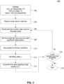
- FIG. 3 depicts an exemplary pseudo code, in accordance with some embodiments.
- FIG. 3 depicts pseudo code to convert a code value in decimal to the shrinking number base described above.
- the algorithm 300 starts at step 302.
- initialization of various variables may be performed.
- num_of_chips may be set to n-1, where n may represent number of frequencies in a continuum. Setting num_of_chips to n-1 guarantees that one frequency form the continuum of n frequencies remains unused.
- n is set to 5, which would set num_of_chips to value 4.
- Base value may be initialized to value of num_of_frequencies, which may be set to 5 for the given example.
- a code value in decimal may be received for conversion to shrinking number base.
- the received code in decimal may be divided by the base value, and remainder of the division operation may be received at step 308.
- the remainder may be recorded as a least significant bit of the code of the shrinking number base.
- quotient of the division operation may be calculated.
- the base value may be decremented by 1.
- a position of the least significant position may be incremented by 1, i.e., left shifted by 1 position.
- value of the quotient and remainder may be checked for 0. If the quotient and the remainder both are of value 0, then the conversion of the code value from decimal to the shrinking base is complete. Otherwise, steps described above with reference to 306 through 316 may be repeated.
- the following table may represent shrinking number base determined as per above algorithm for a partial set of code values with values 0 to 5.
- a person skilled in the art may generate instructions to be executed by the processor 206 to convert each decimal code value of up to 119 and above based on the algorithm described above.
- Table 1 Code value to shrinking base conversion and frequency indices Code Valueshrinking Base Conversion Frequency Indices 0 0 0 0 0 1 2 3 1 1 1 0 0 0 1 0 2 3 2 2 0 0 0 2 0 1 3 3 3 3 0 0 0 3 0 1 2 4 4 0 0 0 0 4 0 1 2 5 0 0 0 0 0 2 1 3
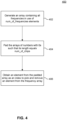
- FIG. 4 depicts an exemplary pseudo code, in accordance with some embodiments.
- FIG. 4 depicts pseudo code to select frequencies corresponding to the code value converted to the shrinking number base as described with reference to FIG. 3 above.
- the algorithm 400 starts at step 402.
- an array containing all frequencies to be used in the n-FSK modulation scheme using half frequencies may be populated.
- the array may be populated with values of the integer frequency dividers corresponding to the frequencies of the n-FSK modulation scheme using half frequencies.
- the array may be populated with frequency values corresponding to each frequency of the n-FSK modulation scheme using half frequencies.
- another array that may represent frequencies corresponding to the code value may be initialized with 0.
- an element from the other array may be selected as an index of the array containing all frequencies to be used in the n-FSK modulation scheme using half frequencies.
- the shrinking base value corresponds to 2, 0, 0, and 0.
- a first frequency may be selected that may correspond to a frequency at an index 2 in the array containing all frequencies populated at step 402. Since, number of frequencies selected should equal to number of chips, i.e., 4 in the given example, three more frequencies need to be selected. Accordingly, step 406 may be repeated for three more times in the given example. Subsequently, frequency at index 0 may be selected when the step 406 is repeated for the first time.
- frequency indices for the decimal code value 0 corresponds to 2, 0, 1, and 3 as described above.
- the frequencies at index 0, 1, 2, 3, and 4 may correspond to the -f chip , -f chip /2, 0, f chip /2, and f chip frequencies respectively.
- code value 2 in decimal may be transmitted using frequencies that may correspond to the center frequency, -f chip frequency, -f chip /2 frequency, and f chip /2 frequency.
- a person skilled in the art may generate instructions to be executed by the processor 206 to determine frequency indices corresponding to each code value in decimal.
- orthogonality of the codes may be required for deconvolution process.
- the frequency scheme may include k frequencies, with equal frequency spacing f space , where k may be calculated as f chip /f space with k having a value between 2 and 6.
- a magnitude dip in the frequency spectrum may be caused during a deconvolution operation.
- the magnitude dip in the frequency spectrum may result in a low signal to noise ratio (SNR) for the decoder during deconvolution process.
- SNR signal to noise ratio
- some codes having a low SNR may be rejected during the deconvolution process.
- the codes which may be rejected during deconvolution process may be referenced as bad codes.
- the following codes may be bad codes for the 5-FSK modulation scheme using half frequencies for the clock frequency of 16 MHz and the target signal bandwidth of 730 Hz.
- Bad code values 0, 19, 33, 34, 38, 39, 59, 60, 80, 81, 85, 86, 100, and 119.
- an optimal signal to noise ratio may be obtained when IQ sampling rate is just in excess of the critical sampling rate.
- the critical sampling rate equals the bandwidth of the signal. So, for a signal with bandwidth of twice the f chip , the sampling frequency may be 2.2 to 2.5 times f chip . This may result in 10 to 25% higher bandwidth to create space for an anti-alias filter.
- IQ signals may be sampled at an rate of 2.44 times f chip for the above described 5-FSK modulation scheme using half frequencies and bandpass filtered, which may result in a signal to noise ratio (SNR) determined as a result of deconvolution process to be of approximately 3.9 compared to 200 when using a matching template.
- SNR signal to noise ratio
- a template may be an ideal signal for the code as transmitted in an IQ sampling format.
- the deconvolution process may include division of the received signal by the template in a frequency space corresponding to code followed by an inverse Fourier transform (IFT).
- IFT inverse Fourier transform
- the SNR of the resulting deconvolution signal may depend on whether the received signal comprises multiple phase shifted copies of the template signal. Accordingly, if the template and the received signal have a matching code value, the SNR of the resulting deconvolution may be between 3.9 to 200 corresponding to a path between the transmitter 102 and the receiver, i.e., the mobile phone 104 or 106. Accordingly, the SNR of below 3.9 may indicate the template code value is different from the transmitted code value.
- the code value which may result in a SNR of below 3.9 after deconvolution process may be considered bad code value and may be avoided.
- a code value that may perform poorly in the deconvolution process may be determined based on assessment criteria.
- the assessment criteria may include verifying nodes in a frequency spectrum of the corresponding code value.
- the assessment criteria may include performing auto-correlation of the frequency spectrum and finding width of the resulting auto-correlation function. Accordingly, codes having excessive auto-correlation width may be identified as bad code values.
- the bad code values should not be used in transmission to carry signaling information.
- auto-correlation width of more than 0.3 may be considered excessive.
- the frequency spacing may be set to half of the f chip frequency.
- a phase change corresponding to the -f chip , -f chip /2, 0, f chip /2, and f chip frequencies may be 0, 180, 0, 180, and 0 degree respectively. Accordingly, a total frequency spacing may be 2 ⁇ f chip .
- While the above disclosed exemplary scheme may use a clock of 16 MHz with number of number chips 4 with 5 different frequencies, there may be many different combinations of frequencies for the code may be generated for different bandwidth. Accordingly, suggested bandwidth may include 500 Hz, 700 Hz, 800 Hz, 730 Hz, 625 Hz, and 40 KHz. Further, each scheme may use different center frequency and different sampling rate. However, bandwidth of 625 Hz with center frequency of 20408 Hz and base clock of 8 MHz may offer the benefit of low bandwidth and addresses issues related to audibility and performance on narrowband signaling better in comparison with other bandwidth schemes described above.
- server processes discussed herein may be implemented using a single server or multiple servers working in combination.
- Databases and applications may be implemented on a single system or distributed across multiple systems. Distributed components may operate sequentially or in parallel.
Landscapes
- Engineering & Computer Science (AREA)
- Computer Networks & Wireless Communication (AREA)
- Signal Processing (AREA)
- Physics & Mathematics (AREA)
- General Physics & Mathematics (AREA)
- Radar, Positioning & Navigation (AREA)
- Remote Sensing (AREA)
- Quality & Reliability (AREA)
- Digital Transmission Methods That Use Modulated Carrier Waves (AREA)
- Transmitters (AREA)
Claims (15)
- Sender (102; 200), umfassend:einen Taktgeber (202), der dazu konfiguriert ist, ein oder mehrere Ausgangstaktsignale zu erzeugen;mindestens einen Frequenzteiler (204), der dazu konfiguriert ist, eine Vielzahl geteilter Frequenzen basierend auf dem einen oder den mehreren Ausgangstaktsignalen zu erzeugen;einen Modulator (210);mindestens eine Antenne (212) oder einen Wandler, der dazu konfiguriert ist, modulierte Daten zu übertragen;einen Speicher (208), der dazu konfiguriert ist, Anweisungen zu speichern; undmindestens einen Prozessor (206), der mit dem Speicher und der mindestens einen Antenne oder dem Wandler gekoppelt ist und dazu konfiguriert ist, die Anweisungen, die Operationen durchführen, auszuführen, umfassend:Abbilden von Daten auf einem Dezimalcodewert aus einer Vielzahl von Dezimalcodewerten;Umwandeln des Dezimalcodewertes in ein Schrumpfbasissystem, wobei das Schrumpfbasissystem nach jeder Teilungsoperation eine Basis dekrementiert; undAuswählen eines Satzes von Frequenzen aus der Vielzahl geteilter Frequenzen basierend auf dem Codewert, der dem Schrumpfbasissystem für den Dezimalcodewert entspricht;wobei der Modulator dazu konfiguriert ist, den Dezimalcodewert unter Verwendung des Satzes von Frequenzen zu modulieren.
- Sender (102; 200) nach Anspruch 1, wobei der Modulator (210) weiter dazu konfiguriert ist, unter Verwendung eines Frequenzumtastungs-Modulationssystems (FSK-Modulationssystems) zu modulieren.
- Sender (102; 200) nach Anspruch 1, wobei der Satz von Frequenzen eine Teilmenge der Vielzahl geteilter Frequenzen ist.
- Sender (102; 200) nach Anspruch 1, wobei der Satz von Frequenzen in einem Ultraschallfrequenzbereich liegt.
- Sender (102; 200) nach Anspruch 1, wobei die Frequenzen in dem Satz von Frequenzen orthogonale Frequenzen sind.
- Sender (102; 200) nach Anspruch 1, wobei ein Gesamtfrequenzabstand der Vielzahl geteilter Frequenzen nicht mehr als das Doppelte einer Chipfrequenz ist.
- Sender (102; 200) nach Anspruch 1, wobei die Operationen weiter umfassen:
Bestimmen einer Vielzahl ganzzahliger Frequenzteilerwerte, um die Vielzahl geteilter Frequenzen zu erzeugen, die einer Signalbandbreite und einer Trägermittenfrequenz entsprechen. - Sender (102; 200) nach Anspruch 1, wobei die Operationen weiter umfassen:Bestimmen einer Chipperiode, die jeder Frequenz der Vielzahl geteilter Frequenzen entspricht,wobei die bestimmte Chipperiode, die jeder Frequenz der Vielzahl geteilter Frequenzen entspricht, die Phasenkontinuität beibehält.
- Sender (102; 200) nach Anspruch 1, wobei die Signalisierungsinformationen Standortinformationen des Senders umfassen.
- Verfahren, umfassend:Empfangen über eine Benutzerschnittstelle einer Taktfrequenz, einer Trägermittenfrequenz, einer Signalbandbreite und einer Zählung zu erzeugender Frequenzen;Bestimmen einer Vielzahl geteilter Frequenzen basierend auf der Taktfrequenz, der Signalbandbreite und der Zählung zu erzeugender Frequenzen;Bestimmen einer Vielzahl ganzzahliger Frequenzteilerwerte, die der Vielzahl geteilter Frequenzen entsprechen;Erzeugen der Vielzahl geteilter Frequenzen durch einen oder mehrere Frequenzteiler;Abbilden von Übertragungsdaten zu einem Dezimalcodewert aus einer Vielzahl von Dezimalcodewerten; undAuswählen eines Satzes von Frequenzen aus der Vielzahl geteilter Frequenzen, die dem Dezimalcodewert zum Modulieren des zu übertragenden Dezimalcodewertes entsprechen.
- Verfahren nach Anspruch 10, wobei die Frequenzen in dem Satz von Frequenzen orthogonale Frequenzen sind.
- Verfahren nach Anspruch 10, wobei das Auswählen des Satzes von Frequenzen weiter umfasst:Umwandeln des Dezimalcodewertes in ein Schrumpfbasissystem, wobei das Schrumpfbasissystem nach jeder Teilungsoperation eine Basis dekrementiert; undAuswählen einer Frequenz, die jedem Wert des Dezimalcodewertes entspricht, basierend auf dem Schrumpfbasissystem, aus der Vielzahl geteilter Frequenzen,wobei sich die Frequenz, die jedem Wert des Dezimalcodewertes basierend auf dem Schrumpfbasissystem entspricht, von jeder anderen unterscheidet.
- Verfahren nach Anspruch 10, wobei das Bestimmen der Vielzahl geteilter Frequenzen weiter das Beibehalten eines Gesamtfrequenzabstands der Vielzahl geteilter Frequenzen von nicht mehr als dem Doppelten einer Chipfrequenz umfasst.
- Verfahren nach Anspruch 10, das weiter das Bestimmen der Orthogonalität des Dezimalcodewertes in dem Dekonvolutionsprozess umfasst, um einen fehlerhaften Dezimalcodewert zu identifizieren.
- Verfahren nach Anspruch 14, wobei das Identifizieren des fehlerhaften Dezimalcodewertes weiter das Durchführen von Autokorrelation eines Frequenzspektrums umfasst, das dem fehlerhaften Dezimalcodewert entspricht, um eine Breite einer Autokorrelationsfunktion zu messen.
Applications Claiming Priority (2)
| Application Number | Priority Date | Filing Date | Title |
|---|---|---|---|
| US16/580,268 US11563607B2 (en) | 2019-09-24 | 2019-09-24 | Orthogonal frequency scheme for narrowband acoustic signaling |
| PCT/IB2020/058856 WO2021059138A1 (en) | 2019-09-24 | 2020-09-22 | Orthogonal frequency scheme for narrowband acoustic signaling |
Publications (3)
| Publication Number | Publication Date |
|---|---|
| EP4035284A1 EP4035284A1 (de) | 2022-08-03 |
| EP4035284B1 true EP4035284B1 (de) | 2024-12-04 |
| EP4035284C0 EP4035284C0 (de) | 2024-12-04 |
Family
ID=72744807
Family Applications (1)
| Application Number | Title | Priority Date | Filing Date |
|---|---|---|---|
| EP20786065.1A Active EP4035284B1 (de) | 2019-09-24 | 2020-09-22 | Orthogonales frequenzschema für schmalbandige akustische signalisierung |
Country Status (8)
| Country | Link |
|---|---|
| US (2) | US11563607B2 (de) |
| EP (1) | EP4035284B1 (de) |
| JP (1) | JP2022549301A (de) |
| KR (1) | KR20220084041A (de) |
| CN (1) | CN114586295A (de) |
| AU (1) | AU2020351726B2 (de) |
| CA (1) | CA3151076A1 (de) |
| WO (1) | WO2021059138A1 (de) |
Families Citing this family (1)
| Publication number | Priority date | Publication date | Assignee | Title |
|---|---|---|---|---|
| US11563607B2 (en) * | 2019-09-24 | 2023-01-24 | Forkbeard Technologies AS | Orthogonal frequency scheme for narrowband acoustic signaling |
Family Cites Families (5)
| Publication number | Priority date | Publication date | Assignee | Title |
|---|---|---|---|---|
| US4109100A (en) * | 1976-09-07 | 1978-08-22 | Raytheon Company | Reverberation compensating communication system |
| US4068198A (en) | 1976-12-23 | 1978-01-10 | Gte Sylvania Incorporated | Phase-locked loop frequency shift key modulator |
| JPH0614065A (ja) * | 1992-06-26 | 1994-01-21 | Nec Corp | 多値fsk変調器 |
| US20090098834A1 (en) | 2006-03-07 | 2009-04-16 | Matsushita Electric Industrial Co., Ltd. | Frequency synthesizer, radio communication system, and semiconductor device |
| US11563607B2 (en) * | 2019-09-24 | 2023-01-24 | Forkbeard Technologies AS | Orthogonal frequency scheme for narrowband acoustic signaling |
-
2019
- 2019-09-24 US US16/580,268 patent/US11563607B2/en active Active
-
2020
- 2020-09-22 EP EP20786065.1A patent/EP4035284B1/de active Active
- 2020-09-22 CN CN202080067070.2A patent/CN114586295A/zh active Pending
- 2020-09-22 KR KR1020227011763A patent/KR20220084041A/ko not_active Ceased
- 2020-09-22 JP JP2022518687A patent/JP2022549301A/ja not_active Withdrawn
- 2020-09-22 AU AU2020351726A patent/AU2020351726B2/en active Active
- 2020-09-22 CA CA3151076A patent/CA3151076A1/en active Pending
- 2020-09-22 WO PCT/IB2020/058856 patent/WO2021059138A1/en not_active Ceased
-
2023
- 2023-01-24 US US18/100,599 patent/US12101209B2/en active Active
Also Published As
| Publication number | Publication date |
|---|---|
| US12101209B2 (en) | 2024-09-24 |
| WO2021059138A1 (en) | 2021-04-01 |
| AU2020351726B2 (en) | 2026-03-05 |
| US20210091986A1 (en) | 2021-03-25 |
| JP2022549301A (ja) | 2022-11-24 |
| EP4035284C0 (de) | 2024-12-04 |
| CA3151076A1 (en) | 2021-04-01 |
| CN114586295A (zh) | 2022-06-03 |
| US11563607B2 (en) | 2023-01-24 |
| AU2020351726A1 (en) | 2022-05-12 |
| US20230318889A1 (en) | 2023-10-05 |
| EP4035284A1 (de) | 2022-08-03 |
| KR20220084041A (ko) | 2022-06-21 |
Similar Documents
| Publication | Publication Date | Title |
|---|---|---|
| US10735230B2 (en) | Wireless communication device, transmitter and methods therein | |
| US11032058B2 (en) | Controlled chaotic system for low probability of detection (LPD) communication | |
| CN110663204B (zh) | 用于建立与一个或多个通信目标一起使用的多个同步信号序列的集合的方法和装备 | |
| CN114667684A (zh) | 反射通信的方法和通信装置 | |
| EP4035284B1 (de) | Orthogonales frequenzschema für schmalbandige akustische signalisierung | |
| WO2024109639A1 (zh) | 资源配置方法、资源确定方法、装置、通信设备及存储介质 | |
| KR100958145B1 (ko) | 펄스진폭변조 파형들의 중첩으로부터 m-진 상위상변조파형을 생성하기 위한 방법 및 장치 | |
| CN115865594A (zh) | 一种基于fdd系统的无源交调校正方法及系统 | |
| US20180097677A1 (en) | Method and apparatus for synchronization | |
| US20230284187A1 (en) | Signal sending method, signal receiving method, and apparatus | |
| US8750420B2 (en) | Method and apparatus for generating modulated radio waves | |
| US20150319519A1 (en) | Digital technique for fm modulation of infrared headphone interface signals | |
| RU2711582C1 (ru) | Способ и система приема сообщений телеметрической информации по рч-каналу | |
| KR20010041026A (ko) | Cdma 통신 시스템에서 클럭 지터에 의해 야기되는위상 에러 보상법 | |
| WO2019111242A1 (en) | Audio transmission and reception | |
| US10573344B2 (en) | Slot synthesis for high cardinality pulse position modulation | |
| JPH07143031A (ja) | スペクトル拡散変調及び/又は復調装置 | |
| RU2854075C2 (ru) | Устройство связи, система связи, способ связи и машиночитаемый носитель данных | |
| US11665033B2 (en) | Transmission device | |
| CN112039543B (zh) | 用于通过射频信道接收遥测消息的片上系统 | |
| JPH07336322A (ja) | 直交周波数分割多重信号送受信装置 | |
| WO2017172439A1 (en) | Frequency shaping and adaptive rounding for o-qpsk and msk transmission in polar coordinates | |
| US20100020888A1 (en) | Communication system, communication method and information recording medium | |
| EP1303061A1 (de) | Telekommunikationssystem mit niedriger parasitärer elektromagnetischer Strahlung | |
| CN118869422A (zh) | 时钟同步方法及其相关设备 |
Legal Events
| Date | Code | Title | Description |
|---|---|---|---|
| STAA | Information on the status of an ep patent application or granted ep patent |
Free format text: STATUS: UNKNOWN |
|
| STAA | Information on the status of an ep patent application or granted ep patent |
Free format text: STATUS: THE INTERNATIONAL PUBLICATION HAS BEEN MADE |
|
| PUAI | Public reference made under article 153(3) epc to a published international application that has entered the european phase |
Free format text: ORIGINAL CODE: 0009012 |
|
| STAA | Information on the status of an ep patent application or granted ep patent |
Free format text: STATUS: REQUEST FOR EXAMINATION WAS MADE |
|
| 17P | Request for examination filed |
Effective date: 20220414 |
|
| AK | Designated contracting states |
Kind code of ref document: A1 Designated state(s): AL AT BE BG CH CY CZ DE DK EE ES FI FR GB GR HR HU IE IS IT LI LT LU LV MC MK MT NL NO PL PT RO RS SE SI SK SM TR |
|
| DAV | Request for validation of the european patent (deleted) | ||
| DAX | Request for extension of the european patent (deleted) | ||
| RAP1 | Party data changed (applicant data changed or rights of an application transferred) |
Owner name: SONITOR TECHNOLOGIES AS |
|
| GRAP | Despatch of communication of intention to grant a patent |
Free format text: ORIGINAL CODE: EPIDOSNIGR1 |
|
| STAA | Information on the status of an ep patent application or granted ep patent |
Free format text: STATUS: GRANT OF PATENT IS INTENDED |
|
| INTG | Intention to grant announced |
Effective date: 20240702 |
|
| GRAS | Grant fee paid |
Free format text: ORIGINAL CODE: EPIDOSNIGR3 |
|
| GRAA | (expected) grant |
Free format text: ORIGINAL CODE: 0009210 |
|
| STAA | Information on the status of an ep patent application or granted ep patent |
Free format text: STATUS: THE PATENT HAS BEEN GRANTED |
|
| AK | Designated contracting states |
Kind code of ref document: B1 Designated state(s): AL AT BE BG CH CY CZ DE DK EE ES FI FR GB GR HR HU IE IS IT LI LT LU LV MC MK MT NL NO PL PT RO RS SE SI SK SM TR |
|
| REG | Reference to a national code |
Ref country code: CH Ref legal event code: EP |
|
| REG | Reference to a national code |
Ref country code: DE Ref legal event code: R096 Ref document number: 602020042580 Country of ref document: DE |
|
| REG | Reference to a national code |
Ref country code: IE Ref legal event code: FG4D |
|
| U01 | Request for unitary effect filed |
Effective date: 20241204 |
|
| U07 | Unitary effect registered |
Designated state(s): AT BE BG DE DK EE FI FR IT LT LU LV MT NL PT RO SE SI Effective date: 20241211 |
|
| PG25 | Lapsed in a contracting state [announced via postgrant information from national office to epo] |
Ref country code: HR Free format text: LAPSE BECAUSE OF FAILURE TO SUBMIT A TRANSLATION OF THE DESCRIPTION OR TO PAY THE FEE WITHIN THE PRESCRIBED TIME-LIMIT Effective date: 20241204 |
|
| PG25 | Lapsed in a contracting state [announced via postgrant information from national office to epo] |
Ref country code: ES Free format text: LAPSE BECAUSE OF FAILURE TO SUBMIT A TRANSLATION OF THE DESCRIPTION OR TO PAY THE FEE WITHIN THE PRESCRIBED TIME-LIMIT Effective date: 20241204 |
|
| PG25 | Lapsed in a contracting state [announced via postgrant information from national office to epo] |
Ref country code: GR Free format text: LAPSE BECAUSE OF FAILURE TO SUBMIT A TRANSLATION OF THE DESCRIPTION OR TO PAY THE FEE WITHIN THE PRESCRIBED TIME-LIMIT Effective date: 20250305 |
|
| PG25 | Lapsed in a contracting state [announced via postgrant information from national office to epo] |
Ref country code: RS Free format text: LAPSE BECAUSE OF FAILURE TO SUBMIT A TRANSLATION OF THE DESCRIPTION OR TO PAY THE FEE WITHIN THE PRESCRIBED TIME-LIMIT Effective date: 20250304 |
|
| PG25 | Lapsed in a contracting state [announced via postgrant information from national office to epo] |
Ref country code: SM Free format text: LAPSE BECAUSE OF FAILURE TO SUBMIT A TRANSLATION OF THE DESCRIPTION OR TO PAY THE FEE WITHIN THE PRESCRIBED TIME-LIMIT Effective date: 20241204 |
|
| PG25 | Lapsed in a contracting state [announced via postgrant information from national office to epo] |
Ref country code: PL Free format text: LAPSE BECAUSE OF FAILURE TO SUBMIT A TRANSLATION OF THE DESCRIPTION OR TO PAY THE FEE WITHIN THE PRESCRIBED TIME-LIMIT Effective date: 20241204 |
|
| PG25 | Lapsed in a contracting state [announced via postgrant information from national office to epo] |
Ref country code: IS Free format text: LAPSE BECAUSE OF FAILURE TO SUBMIT A TRANSLATION OF THE DESCRIPTION OR TO PAY THE FEE WITHIN THE PRESCRIBED TIME-LIMIT Effective date: 20250404 |
|
| PG25 | Lapsed in a contracting state [announced via postgrant information from national office to epo] |
Ref country code: SK Free format text: LAPSE BECAUSE OF FAILURE TO SUBMIT A TRANSLATION OF THE DESCRIPTION OR TO PAY THE FEE WITHIN THE PRESCRIBED TIME-LIMIT Effective date: 20241204 |
|
| PG25 | Lapsed in a contracting state [announced via postgrant information from national office to epo] |
Ref country code: CZ Free format text: LAPSE BECAUSE OF FAILURE TO SUBMIT A TRANSLATION OF THE DESCRIPTION OR TO PAY THE FEE WITHIN THE PRESCRIBED TIME-LIMIT Effective date: 20241204 |
|
| U20 | Renewal fee for the european patent with unitary effect paid |
Year of fee payment: 6 Effective date: 20250811 |
|
| PLBE | No opposition filed within time limit |
Free format text: ORIGINAL CODE: 0009261 |
|
| STAA | Information on the status of an ep patent application or granted ep patent |
Free format text: STATUS: NO OPPOSITION FILED WITHIN TIME LIMIT |
|
| PGFP | Annual fee paid to national office [announced via postgrant information from national office to epo] |
Ref country code: NO Payment date: 20250827 Year of fee payment: 6 |
|
| PGFP | Annual fee paid to national office [announced via postgrant information from national office to epo] |
Ref country code: GB Payment date: 20250814 Year of fee payment: 6 |
|
| 26N | No opposition filed |
Effective date: 20250905 |