EP4033523A1 - Circuit board, electronic device, and electronic module - Google Patents
Circuit board, electronic device, and electronic module Download PDFInfo
- Publication number
- EP4033523A1 EP4033523A1 EP20864731.3A EP20864731A EP4033523A1 EP 4033523 A1 EP4033523 A1 EP 4033523A1 EP 20864731 A EP20864731 A EP 20864731A EP 4033523 A1 EP4033523 A1 EP 4033523A1
- Authority
- EP
- European Patent Office
- Prior art keywords
- protrusions
- face
- conductor
- wiring board
- oblique
- Prior art date
- Legal status (The legal status is an assumption and is not a legal conclusion. Google has not performed a legal analysis and makes no representation as to the accuracy of the status listed.)
- Pending
Links
Images




Classifications
-
- H—ELECTRICITY
- H10—SEMICONDUCTOR DEVICES; ELECTRIC SOLID-STATE DEVICES NOT OTHERWISE PROVIDED FOR
- H10W—GENERIC PACKAGES, INTERCONNECTIONS, CONNECTORS OR OTHER CONSTRUCTIONAL DETAILS OF DEVICES COVERED BY CLASS H10
- H10W70/00—Package substrates; Interposers; Redistribution layers [RDL]
- H10W70/60—Insulating or insulated package substrates; Interposers; Redistribution layers
-
- H—ELECTRICITY
- H10—SEMICONDUCTOR DEVICES; ELECTRIC SOLID-STATE DEVICES NOT OTHERWISE PROVIDED FOR
- H10W—GENERIC PACKAGES, INTERCONNECTIONS, CONNECTORS OR OTHER CONSTRUCTIONAL DETAILS OF DEVICES COVERED BY CLASS H10
- H10W70/00—Package substrates; Interposers; Redistribution layers [RDL]
- H10W70/40—Leadframes
- H10W70/411—Chip-supporting parts, e.g. die pads
-
- H—ELECTRICITY
- H05—ELECTRIC TECHNIQUES NOT OTHERWISE PROVIDED FOR
- H05K—PRINTED CIRCUITS; CASINGS OR CONSTRUCTIONAL DETAILS OF ELECTRIC APPARATUS; MANUFACTURE OF ASSEMBLAGES OF ELECTRICAL COMPONENTS
- H05K1/00—Printed circuits
- H05K1/02—Details
- H05K1/0271—Arrangements for reducing stress or warp in rigid printed circuit boards, e.g. caused by loads, vibrations or differences in thermal expansion
-
- H—ELECTRICITY
- H10—SEMICONDUCTOR DEVICES; ELECTRIC SOLID-STATE DEVICES NOT OTHERWISE PROVIDED FOR
- H10W—GENERIC PACKAGES, INTERCONNECTIONS, CONNECTORS OR OTHER CONSTRUCTIONAL DETAILS OF DEVICES COVERED BY CLASS H10
- H10W70/00—Package substrates; Interposers; Redistribution layers [RDL]
- H10W70/40—Leadframes
- H10W70/421—Shapes or dispositions
-
- H—ELECTRICITY
- H10—SEMICONDUCTOR DEVICES; ELECTRIC SOLID-STATE DEVICES NOT OTHERWISE PROVIDED FOR
- H10W—GENERIC PACKAGES, INTERCONNECTIONS, CONNECTORS OR OTHER CONSTRUCTIONAL DETAILS OF DEVICES COVERED BY CLASS H10
- H10W70/00—Package substrates; Interposers; Redistribution layers [RDL]
- H10W70/60—Insulating or insulated package substrates; Interposers; Redistribution layers
- H10W70/62—Insulating or insulated package substrates; Interposers; Redistribution layers characterised by their interconnections
- H10W70/65—Shapes or dispositions of interconnections
-
- H—ELECTRICITY
- H10—SEMICONDUCTOR DEVICES; ELECTRIC SOLID-STATE DEVICES NOT OTHERWISE PROVIDED FOR
- H10W—GENERIC PACKAGES, INTERCONNECTIONS, CONNECTORS OR OTHER CONSTRUCTIONAL DETAILS OF DEVICES COVERED BY CLASS H10
- H10W70/00—Package substrates; Interposers; Redistribution layers [RDL]
- H10W70/60—Insulating or insulated package substrates; Interposers; Redistribution layers
- H10W70/62—Insulating or insulated package substrates; Interposers; Redistribution layers characterised by their interconnections
- H10W70/65—Shapes or dispositions of interconnections
- H10W70/652—Cross-sectional shapes
- H10W70/6525—Cross-sectional shapes for securing the interconnections to the substrate, e.g. to prevent peeling
-
- H—ELECTRICITY
- H05—ELECTRIC TECHNIQUES NOT OTHERWISE PROVIDED FOR
- H05K—PRINTED CIRCUITS; CASINGS OR CONSTRUCTIONAL DETAILS OF ELECTRIC APPARATUS; MANUFACTURE OF ASSEMBLAGES OF ELECTRICAL COMPONENTS
- H05K1/00—Printed circuits
- H05K1/02—Details
- H05K1/11—Printed elements for providing electric connections to or between printed circuits
- H05K1/111—Pads for surface mounting, e.g. lay-out
-
- H—ELECTRICITY
- H05—ELECTRIC TECHNIQUES NOT OTHERWISE PROVIDED FOR
- H05K—PRINTED CIRCUITS; CASINGS OR CONSTRUCTIONAL DETAILS OF ELECTRIC APPARATUS; MANUFACTURE OF ASSEMBLAGES OF ELECTRICAL COMPONENTS
- H05K2201/00—Indexing scheme relating to printed circuits covered by H05K1/00
- H05K2201/09—Shape and layout
- H05K2201/09009—Substrate related
- H05K2201/09045—Locally raised area or protrusion of insulating substrate
-
- H—ELECTRICITY
- H05—ELECTRIC TECHNIQUES NOT OTHERWISE PROVIDED FOR
- H05K—PRINTED CIRCUITS; CASINGS OR CONSTRUCTIONAL DETAILS OF ELECTRIC APPARATUS; MANUFACTURE OF ASSEMBLAGES OF ELECTRICAL COMPONENTS
- H05K2201/00—Indexing scheme relating to printed circuits covered by H05K1/00
- H05K2201/09—Shape and layout
- H05K2201/09209—Shape and layout details of conductors
- H05K2201/09372—Pads and lands
- H05K2201/0939—Curved pads, e.g. semi-circular or elliptical pads or lands
-
- H—ELECTRICITY
- H05—ELECTRIC TECHNIQUES NOT OTHERWISE PROVIDED FOR
- H05K—PRINTED CIRCUITS; CASINGS OR CONSTRUCTIONAL DETAILS OF ELECTRIC APPARATUS; MANUFACTURE OF ASSEMBLAGES OF ELECTRICAL COMPONENTS
- H05K2201/00—Indexing scheme relating to printed circuits covered by H05K1/00
- H05K2201/09—Shape and layout
- H05K2201/09209—Shape and layout details of conductors
- H05K2201/09372—Pads and lands
- H05K2201/09409—Multiple rows of pads, lands, terminals or dummy patterns; Multiple rows of mounted components
-
- H—ELECTRICITY
- H05—ELECTRIC TECHNIQUES NOT OTHERWISE PROVIDED FOR
- H05K—PRINTED CIRCUITS; CASINGS OR CONSTRUCTIONAL DETAILS OF ELECTRIC APPARATUS; MANUFACTURE OF ASSEMBLAGES OF ELECTRICAL COMPONENTS
- H05K2201/00—Indexing scheme relating to printed circuits covered by H05K1/00
- H05K2201/09—Shape and layout
- H05K2201/09209—Shape and layout details of conductors
- H05K2201/09372—Pads and lands
- H05K2201/09418—Special orientation of pads, lands or terminals of component, e.g. radial or polygonal orientation
-
- H—ELECTRICITY
- H05—ELECTRIC TECHNIQUES NOT OTHERWISE PROVIDED FOR
- H05K—PRINTED CIRCUITS; CASINGS OR CONSTRUCTIONAL DETAILS OF ELECTRIC APPARATUS; MANUFACTURE OF ASSEMBLAGES OF ELECTRICAL COMPONENTS
- H05K2203/00—Indexing scheme relating to apparatus or processes for manufacturing printed circuits covered by H05K3/00
- H05K2203/03—Metal processing
- H05K2203/0307—Providing micro- or nanometer scale roughness on a metal surface, e.g. by plating of nodules or dendrites
-
- H—ELECTRICITY
- H05—ELECTRIC TECHNIQUES NOT OTHERWISE PROVIDED FOR
- H05K—PRINTED CIRCUITS; CASINGS OR CONSTRUCTIONAL DETAILS OF ELECTRIC APPARATUS; MANUFACTURE OF ASSEMBLAGES OF ELECTRICAL COMPONENTS
- H05K3/00—Apparatus or processes for manufacturing printed circuits
- H05K3/38—Improvement of the adhesion between the insulating substrate and the metal
- H05K3/382—Improvement of the adhesion between the insulating substrate and the metal by special treatment of the metal
- H05K3/384—Improvement of the adhesion between the insulating substrate and the metal by special treatment of the metal by plating
-
- H—ELECTRICITY
- H10—SEMICONDUCTOR DEVICES; ELECTRIC SOLID-STATE DEVICES NOT OTHERWISE PROVIDED FOR
- H10W—GENERIC PACKAGES, INTERCONNECTIONS, CONNECTORS OR OTHER CONSTRUCTIONAL DETAILS OF DEVICES COVERED BY CLASS H10
- H10W70/00—Package substrates; Interposers; Redistribution layers [RDL]
- H10W70/60—Insulating or insulated package substrates; Interposers; Redistribution layers
- H10W70/62—Insulating or insulated package substrates; Interposers; Redistribution layers characterised by their interconnections
- H10W70/65—Shapes or dispositions of interconnections
- H10W70/657—Shapes or dispositions of interconnections on sidewalls or bottom surfaces of the package substrates, interposers or redistribution layers
-
- H—ELECTRICITY
- H10—SEMICONDUCTOR DEVICES; ELECTRIC SOLID-STATE DEVICES NOT OTHERWISE PROVIDED FOR
- H10W—GENERIC PACKAGES, INTERCONNECTIONS, CONNECTORS OR OTHER CONSTRUCTIONAL DETAILS OF DEVICES COVERED BY CLASS H10
- H10W70/00—Package substrates; Interposers; Redistribution layers [RDL]
- H10W70/60—Insulating or insulated package substrates; Interposers; Redistribution layers
- H10W70/62—Insulating or insulated package substrates; Interposers; Redistribution layers characterised by their interconnections
- H10W70/66—Conductive materials thereof
-
- H—ELECTRICITY
- H10—SEMICONDUCTOR DEVICES; ELECTRIC SOLID-STATE DEVICES NOT OTHERWISE PROVIDED FOR
- H10W—GENERIC PACKAGES, INTERCONNECTIONS, CONNECTORS OR OTHER CONSTRUCTIONAL DETAILS OF DEVICES COVERED BY CLASS H10
- H10W70/00—Package substrates; Interposers; Redistribution layers [RDL]
- H10W70/60—Insulating or insulated package substrates; Interposers; Redistribution layers
- H10W70/67—Insulating or insulated package substrates; Interposers; Redistribution layers characterised by their insulating layers or insulating parts
- H10W70/68—Shapes or dispositions thereof
Definitions
- the present disclosure relates to a wiring board, an electronic device, and an electronic module.
- Many electronic devices include a wiring board including a base and a thin film conductor formed on a principal surface of the base (see, for example, Japanese Unexamined Patent Application Publication No. 2001-244626 ).
- a wiring board includes a base having a first face and a conductor positioned on the first face.
- the conductor has a region in which a plurality of first protrusions are positioned on a surface of the conductor, the plurality of first protrusions protruding in a same oblique direction that is oblique to a direction normal to the first face.
- An electronic device includes the above-described wiring board and an electronic component mounted on the wiring board.
- An electronic module includes the above-described electronic device and a module substrate on which the electronic device is mounted.
- FIG. 1 is a perspective view of a wiring board according to a first embodiment of the present disclosure.
- a conductor 20 is partially cut away.
- a wiring board 1 according to the first embodiment includes a base 10 having a first face 11 and a conductor 20 that extends over the first face 11.
- the base 10 may be composed of an aluminum oxide (Al 2 O 3 ) based sintered body, which is an insulator, a silicon carbide (SiC) substrate, which is a conductor, or other materials.
- the conductor 20 may be a thin film conductor, and may be formed by a sputtering method or a deposition method, such as vacuum deposition or chemical vapor deposition (CVD).
- the conductor 20 extends over the entire area of the first face 11 of the base 10 in Fig. 1 , the conductor 20 may instead be formed on the first face 11 in any pattern.
- the conductor 20 may be provided on each of the first face 11 and a second face 12.
- Fig. 2 is a conceptual diagram (sectional view) illustrating the structure of a surface of the wiring board illustrated in Fig. 1 .
- the conductor 20 has a region in which a plurality of first protrusions 21a are positioned on a surface thereof.
- the first protrusions 21a protrude in the same oblique direction that is oblique to the Z direction.
- the above-described region may extend over either the entire area or a portion of the conductor 20.
- the region extends in the X direction and the Y direction, and many first protrusions 21a may be arranged in the X direction and the Y direction.
- the Z direction corresponds to a direction normal to the first face 11.
- the X direction and the Y direction are two directions that extend along the first face 11 and that are orthogonal to each other.
- the conductor 20 may have a structure including many granules 21 arranged in a certain direction, and the first protrusions 21a may be end portions of the granules 21.
- the granules 21 may be either crystalline grains or polycrystalline grains.
- the end portion of each granule 21 has a width less than the width of a body portion of the granule 21, and the body portions of adjacent ones of the granules 21 are in contact with each other.
- the granules 21 may be distinguished from each other by forming a cross section thereof with an ion beam, such as a focused ion beam (FIB), and observing the cross section with an electron microscope, such as a scanning electron microscope (SEM).
- FIB focused ion beam
- SEM scanning electron microscope
- the first protrusions 21a protrude in a direction oblique to the Z direction.
- the long-side direction of each granule 21 is inclined with respect to the Z direction.
- the inclination angle may be in the range of, for example, 10° to 60° or 35° to 55°.
- the first protrusions 21a protrude in substantially the same direction (for example, direction inclined by a certain angle from the Z direction toward the Y direction).
- Fig. 3 is a diagram (sectional view) illustrating the detailed structure of a surface of the conductor.
- the Y direction direction toward which the first protrusions 21a are inclined
- the Z direction is upward.
- the conductor 20 includes a portion in which a section Q1 adjacent to a first protrusion 21aA has an outline curved convexly in a direction coinciding with the oblique direction in which the first protrusions 21a protrude.
- two first protrusions 21aA and 21aB are adjacent to each other.
- the granules 21 include two granules 21A and 21B that are adjacent to each other in the left-right direction and that the first protrusions 21a include the first protrusions 21aA and 21aB of the granules 21A and 21B, respectively.
- a right end P1 of the left first protrusion 21aA is to the right and above a contact end P2 between the left and right first protrusions 21aA and 21aB.
- the cross section is orthogonal to corners between the first face 11 and side faces of the base 10, and extends along the Y-Z plane in the example illustrated in Figs. 2 and 3 .
- the joining material enters the space between the two adjacent first protrusions 21aA and 21aB and is cured. Then, if a tensile force is applied to the electronic component in the Z direction, the cured joining material is caught in the region between the contact end P2 of the pair of first protrusions 21aA and 21aB and the right end P1 of the first protrusion 21aA and exhibits an anchoring effect that increases the strength between the cured joining material and the conductor 20. Accordingly, even if a large force is applied to the electronic component, the electronic component is not easily separated from the wiring board 1.
- a joining material such as solder or conductive paste
- the direction in which a boundary line S1 between the pair of first protrusions 21aA and 21aB that are adjacent to each other in the left-right direction extends is the direction coinciding with the oblique direction in which the first protrusions 21a protrude.
- the boundary line S1 is the section line of the interface between the pair of granules 21A and 21B that are adjacent to each other in the left-right direction.
- the interface corresponds to a grain boundary if the granules 21A and 21B are crystalline grains, and corresponds to an interface (grain boundary) between crystalline grains that belong to the granule 21A and crystalline grains that belong to the granule 21B if the granules 21A and 21B are polycrystalline grains.
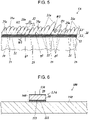
- Fig. 4A is a diagram (sectional view) illustrating the stress generated in the conductor.
- Fig. 4B is a diagram (sectional view) illustrating the stress generated in a conductor according to a comparative example. Due to a difference in coefficient of thermal expansion between the conductor 20 and the base 10, if the conductor 20 is cooled after a high-temperature formation process, a stress F1 may be generated in the conductor 20 in a direction along the first face 11. In such a case, if an interface S8 between granules 81A and 81B extends in the Z direction as in the comparative example illustrated in Fig. 4B , the stress F1 is directly applied in a direction in which separation occurs at the interface S8.
- boundary line S1 is inclined with respect to the Z direction as in the first embodiment illustrated in Fig. 4A , a component F1a of the stress F1 is directed in a direction along the boundary line S1, and a component F1b of the stress F1 in a direction in which separation occurs at the interface (boundary line S1) is reduced. Therefore, the disruptive strength of the conductor 20 against the stress is increased, and cracks are not easily formed in the conductor 20 due to the stress. As a result, the occurrence of mounting failure of the electronic component due to breakage of the conductor 20 can be reduced.
- a plurality of cavities g1 are formed in the conductor 20 in the region in which the first protrusions 21a are provided.
- Each space g1 corresponds to a gap between an adjacent pair of the granules 21.
- the long-side direction of each space g1 is the oblique direction coinciding with the direction in which the first protrusions 21a protrudes.
- the inclined cavities g1 serve to buffer the stress F1 in the direction along the first face 11 and the direction perpendicular to the first face 11. More specifically, the cavities g1 are reduced in size in the short-side direction thereof to exhibit the buffering effect. Since the long-side direction H and the short-side direction of each space g1 are oblique to the first face 11, the cavities g1 exhibit the buffering effect in the direction along the first face 11 and the direction perpendicular to the first face 11.
- the first protrusions 21a on the surface of the conductor 20 protrude obliquely to the Z direction. Accordingly, if the electronic component is mounted, the strength of the mounting portion can be increased.
- FIG. 5 is a conceptual diagram (sectional view) illustrating the structure of a surface of a wiring board according to a second embodiment of the present disclosure.
- a wiring board 1A according to the second embodiment includes a conductor 20 including a first layer L1 and a second layer L2 that is in contact with the first layer L1 and positioned on the first face 11.
- the first layer L1 may be, for example, a main conductor layer made of a metal having a low electrical resistance, such as gold (Au) or copper (Cu).
- the second layer L2 may be, for example, an adhesion layer made of a highly adhesive metal, such as titanium (Ti), or a barrier layer positioned between an adhesion layer and the main conductor layer.
- the second layer L2 has a region in which a plurality of second protrusions 25a are positioned.
- the second protrusions 25a protrude in the same oblique direction that is oblique to the Z direction.
- Many second protrusions 25a may be arranged in the X direction and the Y direction.
- the second layer L2 may include many granules 25 arranged in a certain direction.
- the second protrusions 25a may be end portions of the granules 25.
- the granules 25 may be either crystalline grains or polycrystalline grains.
- the end portion of each granule 25 has a width less than the width of a body portion of the granule 25, and the body portions of adjacent ones of the granules 25 are in contact with each other.
- First protrusions 21a and granules 21 of the first layer L1 are similar to those described in the first embodiment except that they are in contact with the second layer L2 and disposed on the second layer L2.
- the direction in which the second protrusions 25a and the granules 25 of the second layer L2 are oriented and the direction in which the first protrusions 21a and the granules 21 of the first layer L1 are oriented may be either substantially the same direction or different oblique directions.
- the first layer L1 is present between the first protrusions 21a in a lower section thereof. In this region, the first layer L1 may have portions sandwiched between the protrusions 25a of the second layer L2 in the lower section thereof.
- the second protrusions 25a have a width W2 less than a width W1 of the first protrusions 21a.
- the second protrusions 25a have a height H2 less than a height H1 of the first protrusions 21a.
- the second protrusions 25a are arranged at a pitch J2 less than a pitch J1 at which the first protrusions 21a are arranged. These comparisons may be based on averages excluding extreme values. The extreme values to be excluded may be highest 10% and lowest 10% of all values.
- the pitch J1 is, for example, 100 to 1000 [nm]
- the pitch J2 is, for example, 10 to 100 [nm].
- the wiring board 1A according to the second embodiment includes the first layer L1 including the first protrusions 21a. Therefore, similarly to the wiring board 1 according to the first embodiment, the strength of a joining portion of a mounted component can be increased.
- the second layer L2 is provided between the first layer L1 and the base 10. Furthermore, the second layer L2 has a region in which the second protrusions 25a are provided.
- the second protrusions 25a which are arranged at a small pitch and have small dimensions, protrude obliquely to the Z direction. In the above-described region, the first layer L1 is present between the second protrusions 25a.
- the base 10 and the first layer L1 can be strongly joined together. As a result, even if a large stress is generated in the conductor 20 due to a difference in coefficient of thermal expansion between the base 10 and the conductor 20, or if a very large force is applied to the mounted component, the conductor 20 is not easily separated from the base 10.
- Fig. 6 is a sectional view of an electronic device and an electronic module according to an embodiment.
- An electronic device 160 includes the wiring board 1 (or wiring board 1A) and an electronic component 150 mounted on the wiring board 1 or 1A.
- the electronic component 150 may be various types of electronic components, and examples thereof include an optical element, an imaging element, a piezoelectric vibrator such as a crystal vibrator, various types of sensors such as a motion sensor, a surface acoustic wave device, a semiconductor device such as a semiconductor integrated circuit (IC) device, a capacitive element, an inductor element, and a resistor.
- IC semiconductor integrated circuit
- the electronic component 150 may be joined to the conductor 20 of the wiring board 1 or 1A with a joining material, such as solder or conductive paste.
- the conductor 20 may have a function of transmitting signals or electric power to or from the electronic component 150.
- the conductor 20 may have no electrical function and be joined to the electronic component 150 to support the electronic component 150.
- An electronic module 100 includes a module substrate 110 and the electronic device 160 mounted on the module substrate 110.
- the module substrate 110 may also have other electronic devices, electronic elements, and electrical elements mounted thereon.
- An electrode pad 111 may be provided on the module substrate 110, and the electronic device 160 may be joined to the electrode pad 111 with a joining material 113, such as solder.
- the electronic device 160 and the electronic module 100 include the wiring board 1 or 1A in which the mounting portion has a high strength and in which the conductor 20 and the base 10 are strongly joined together. Therefore, the reliability can be increased. Even if, for example, a strong vibration or a large acceleration is applied to the electronic device 160 or the electronic module 100, the occurrence of mounting failure of the electronic component 150 can be reduced, and the reliability can thus be increased.
- the wiring board, the electronic device, and the electronic module according to the present disclosure are not limited to those in the above-described embodiments.
- the protrusions of the conductor have a smooth shape in the conceptual diagrams of the above-described embodiments, the protrusions may instead have an angular shape or a pointed shape.
- the protrusions may be provided over a portion of the surface of the conductor instead of the entire area thereof.
- the details described in the embodiments, such as the inclination angle and the pitch of the granules or the protrusions, may be changed as appropriate without departing from the spirit of the invention.
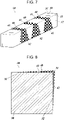
- FIG. 7 is a perspective view of a wiring board according to a third embodiment.
- Fig. 8 is a sectional view of the wiring board according to the third embodiment.
- a wiring board 1B according to the third embodiment includes a base 30 having first faces 31 and 32 and conductors 40 positioned on the first faces 31 and 32.
- the base 30 is an insulator.
- the first faces 31 and 32 may be adjacent to each other with a corner portion 33 disposed therebetween.
- the first face 31 and the first face 32 may have different surface roughnesses.
- the conductors 40 include first conductors 41 positioned on the first face 31 and second conductors 42 positioned on the first face 32.
- the first conductors 41 may be connected to the second conductors 42 at the corner portion 33.
- the first conductors 41 and the second conductors 42 may have patterns of predetermined shapes on the first faces 31 and 32.
- the first conductors 41 may have a thickness that increases toward the corner portion 33.
- the second conductors 42 may have a thickness that increases toward the corner portion 33.
- the first conductors 41 have a plurality of first protrusions that protrude in the same oblique direction that is oblique to a direction normal to the first face 31.
- the first conductors 41 may also have a plurality of second protrusions that protrude in the same oblique direction that is oblique to the direction normal to the first face 31.
- the second conductors 42 have a plurality of first protrusions that protrude in the same oblique direction that is oblique to a direction normal to the first face 32.
- the second conductors 42 may also have a plurality of second protrusions that protrude in the same oblique direction that is oblique to the direction normal to the first face 32.
- the first protrusions and the second protrusions are similar to those described in the first and second embodiments.
- the wiring board 1B may be structured such that a mounting section, in which an electronic component is mounted, is positioned on the first face 31 and that a wire connection section, which is subjected to wire bonding, is positioned on the first face 32.
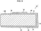
- FIG. 9 is a sectional view of a wiring board according to a fourth embodiment.
- Fig. 10 is a plan view of the wiring board according to the fourth embodiment.
- Fig. 9 shows a cross section of Fig. 10 taken along line A-A.
- a wiring board 1C according to the fourth embodiment includes a base 50 having a first face 51, a second face 52, and a side face 53; a metal film 60 positioned on both the first face 51 and the side face 53; a metal film 61 positioned on both the second face 52 and the side face 53; a wiring conductor 62 positioned on the metal film 60; and a wiring conductor 63 positioned on the metal film 61.
- the base 50 is an insulator.
- the first face 51 and the second face 52 face away from each other.
- the side face 53 is positioned between the first face 51 and the second face 52 and is adjacent to each of the first face 51 and the second face 52 with a corner portion provided therebetween.
- the metal film 60 has marks 60a to 60c ( Fig. 10 ) formed in a predetermined pattern composed of sections in which the metal film 60 is formed and sections in which the metal film 60 is not formed.
- the metal film 60 and the metal film 61 at least partially overlap on the side face 53.
- the metal film 60 has a thickness that increases toward the corner portion between the first face 51 and the side face 53.
- the metal film 61 has a thickness that increases toward the corner portion between the second face 52 and the side face 53.
- the metal films 60 and 61 correspond to a conductor according to the present disclosure.
- a portion of the metal film 60 that is positioned on the first face 51 has a plurality of first protrusions that protrude in the same oblique direction that is oblique to a direction normal to the first face 51.
- the portion of the metal film 60 positioned on the first face 51 may also have a plurality of second protrusions that protrude in the same oblique direction that is oblique to the direction normal to the first face 51.
- a portion of the metal film 60 that is positioned on the side face 53 has a plurality of first protrusions that protrude in the same oblique direction that is oblique to a direction normal to the side face 53.
- the portion of the metal film 60 positioned on the side face 53 may also have a plurality of second protrusions that protrude in the same oblique direction that is oblique to the direction normal to the side face 53.
- a portion of the metal film 61 that is positioned on the second face 52 has a plurality of first protrusions that protrude in the same oblique direction that is oblique to a direction normal to the second face 52.
- the portion of the metal film 61 positioned on the second face 52 may also have a plurality of second protrusions that protrude in the same oblique direction that is oblique to the direction normal to the second face 52.
- a portion of the metal film 61 that is positioned on the side face 53 (in the direction perpendicular to the side face 53) has a plurality of first protrusions that protrude in the same oblique direction that is oblique to a direction normal to the side face 53.
- the portion of the metal film 61 positioned on the side face 53 may also have a plurality of second protrusions that protrude in the same oblique direction that is oblique to the direction normal to the side face 53.
- the wiring conductors 62 and 63 may correspond to the conductor according to the present disclosure. More specifically, the wiring conductor 62 has a plurality of first protrusions that protrude in the same oblique direction that is oblique to a direction normal to the first face 51 or a surface of the metal film 60. The wiring conductor 62 may also have a plurality of second protrusions that protrude in the same oblique direction that is oblique to the direction normal to the first face 51 or the surface of the metal film 60.
- the wiring conductor 63 has a plurality of first protrusions that protrude in the same oblique direction that is oblique to a direction normal to the second face 52 or a surface of the metal film 61.
- the wiring conductor 63 may also have a plurality of second protrusions that protrude in the same oblique direction that is oblique to the direction normal to the second face 52 or the surface of the metal film 61.
- the first protrusions and the second protrusions are similar to those described in the first and second embodiments.
- the wiring board 1C may be structured such that a mounting section, in which an electronic component is mounted, is positioned on the wiring conductor 62 and that a surface of the wiring conductor 63 serves as a joining surface to be joined to a module substrate with a joining material.
- FIG. 11 is a perspective view of a wiring board according to a fifth embodiment.
- a wiring board 1D according to the fifth embodiment includes a base 70D having three or more faces (an upper face 71D, one side face 72D having no wiring conductors 81D, and one side face that is not visible in Fig. 11 ) that are oriented in different directions and on each of which an electronic component can be mounted and one face (bottom face that is not visible in Fig. 11 ) that is to be joined to a module substrate.
- the upper face 71D and the bottom face of the base 70D have recessed steps at peripheral edges of the upper face 71D and peripheral edges of the bottom face.
- the base 70D is an insulator.
- the upper face 71D, four side faces 72D, and the bottom face correspond to a first face according to the present disclosure.
- the wiring board 1D also includes wiring conductors 81D and 82D positioned on surfaces of the base 70D.
- the wiring conductors 81D and 82D are conductors to be electrically connected to electrodes of electronic components mounted on the above-mentioned three or more faces with bonding wires or a conductive joining material, such as solder.
- the wiring conductors 81D are positioned to extend along the upper face 71D, one side face 72D, and the bottom face of the base 70D.
- the wiring conductors 82D are positioned to extend along the side face 72D and the bottom face of the base 70D.
- the wiring conductors 81D and 82D correspond to the conductor according to the present disclosure. Portions of the wiring conductors 81D that are positioned on the upper face 71D have a plurality of first protrusions that protrude in the same oblique direction that is oblique to a direction normal to the upper face 71D. The portions of the wiring conductors 81D positioned on the upper face 71D may also have a plurality of second protrusions that protrude in the same oblique direction that is oblique to the direction normal to the upper face 71D.
- Portions of the wiring conductors 81D that are positioned on the side face 72D have a plurality of first protrusions that protrude in the same oblique direction that is oblique to a direction normal to the side face 72D.
- the portions of the wiring conductors 81D positioned on the side face 72D may also have a plurality of second protrusions that protrude in the same oblique direction that is oblique to the direction normal to the side face 72D.
- Portions of the wiring conductors 81D that are positioned on the bottom face of the base 70D have a plurality of first protrusions that protrude in the same oblique direction that is oblique to a direction normal to the bottom face.
- the portions of the wiring conductors 81D positioned on the bottom face may also have a plurality of second protrusions that protrude in the same oblique direction that is oblique to the direction normal to the bottom face.
- Portions of the wiring conductors 82D that are positioned on the side face 72D have a plurality of first protrusions that protrude in the same oblique direction that is oblique to a direction normal to the side face 72D.
- the portions of the wiring conductors 82D positioned on the side face 72D may also have a plurality of second protrusions that protrude in the same oblique direction that is oblique to the direction normal to the side face 72D.
- Portions of the wiring conductors 82D that are positioned on the bottom face of the base 70D have a plurality of first protrusions that protrude in the same oblique direction that is oblique to a direction normal to the bottom face.
- the portions of the wiring conductors 82D positioned on the bottom face may also have a plurality of second protrusions that protrude in the same oblique direction that is oblique to the direction normal to the bottom face.
- the first protrusions and the second protrusions are similar to those described in the first and second embodiments.
- FIG. 12 is a perspective view of a wiring board according to a sixth embodiment.
- a wiring board 1E according to the sixth embodiment includes a base 70E, which is an insulator, and wiring conductors 81E and 84E positioned on surfaces of the base 70E.
- the base 70E includes a cubic portion having three or more faces (an upper face 71E, one side face 72E having no wiring conductors 81E, and one side face that is not visible in Fig. 12 ) that are oriented in different directions and on each of which an electronic component can be mounted; and a plate-shaped portion 74E that spreads at the bottom of the cubic portion.
- the upper face 71E of the base 70E has recessed steps at peripheral edges of the upper face 71E.
- the upper face 71E, four side faces, and an upper face 75E of the plate-shaped portion 74E correspond to the first face of the present disclosure.
- the wiring conductors 81E and 84E are conductors to be electrically connected to electrodes of electronic components mounted on the above-mentioned three or more faces with bonding wires or a conductive joining material, such as solder.
- the wiring conductors 81E are positioned to extend along the upper face 71E and one side face 72E of the base 70E and the upper face 75E of the plate-shaped portion 74E.
- the wiring conductors 84E are positioned to extend along the side face 72E of the base 70E and the upper face 75E of the plate-shaped portion 74E.
- the wiring conductors 81E and 84E correspond to the conductor according to the present disclosure. Portions of the wiring conductors 81E that are positioned on the upper face 71E have a plurality of first protrusions that protrude in the same oblique direction that is oblique to a direction normal to the upper face 71E. The portions of the wiring conductors 81E positioned on the upper face 71E may also have a plurality of second protrusions that protrude in the same oblique direction that is oblique to the direction normal to the upper face 71E.
- Portions of the wiring conductors 81E that are positioned on the side face 72E have a plurality of first protrusions that protrude in the same oblique direction that is oblique to a direction normal to the side face 72E.
- the portions of the wiring conductors 81E positioned on the side face 72E may also have a plurality of second protrusions that protrude in the same oblique direction that is oblique to the direction normal to the side face 72E.
- Portions of the wiring conductors 81E that are positioned on the upper face 75E of the plate-shaped portion 74E have a plurality of first protrusions that protrude in the same oblique direction that is oblique to a direction normal to the upper face 75E.
- the portions of the wiring conductors 81E positioned on the upper face 75E of the plate-shaped portion 74E may also have a plurality of second protrusions that protrude in the same oblique direction that is oblique to the direction normal to the upper face 75E.
- Portions of the wiring conductors 84E that are positioned on the side face 72E have a plurality of first protrusions that protrude in the same oblique direction that is oblique to a direction normal to the side face 72E.
- the portions of the wiring conductors 84E positioned on the side face 72E may also have a plurality of second protrusions that protrude in the same oblique direction that is oblique to the direction normal to the side face 72E.
- Portions of the wiring conductors 84E that are positioned on the upper face 75E of the plate-shaped portion 74E have a plurality of first protrusions that protrude in the same oblique direction that is oblique to a direction normal to the upper face 75E.
- the portions of the wiring conductors 84E positioned on the upper face 75E of the plate-shaped portion 74E may also have a plurality of second protrusions that protrude in the same oblique direction that is oblique to the direction normal to the upper face 75E.
- the first protrusions and the second protrusions are similar to those described in the first and second embodiments.
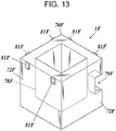
- FIG. 13 is a perspective view of a wiring board according to a seventh embodiment.
- a wiring board 1F according to the seventh embodiment includes a base 70F having the shape of a polyhedron with hollow spaces and wiring conductors 81F positioned on outer faces 72F of the base 70F.
- the base 70F may have a hollow space 78F that extends from the center to one side of the polyhedron.
- the base 70F may also have a hollow space 79F that is exposed at a side portion of the polyhedron.
- the base 70F is an insulator.
- Some of the outer faces 72F of the base 70F each serve as a mounting section in which an electronic component is mounted, and these outer faces 72F correspond to the first face according to the present disclosure.
- the wiring conductors 81F are conductors to be electrically connected to electrodes of electronic components mounted on the outer faces 72F with bonding wires or a conductive joining material, such as solder.
- Each wiring conductor 81F has a plurality of first protrusions that protrude in the same oblique direction that is oblique to a direction normal to the outer face 72F of the base 70F on which the wiring conductor 81F is provided.
- Each wiring conductor 81F may also have a plurality of second protrusions that protrude in the same oblique direction that is oblique to the direction normal to the outer face 72F of the base 70F on which the wiring conductor 81F is positioned.
- the first protrusions and the second protrusions are similar to those described in the first and second embodiments.
- the conductors having the first protrusions or both the first protrusions and the second protrusions function advantageously if used in combination with bases of various wiring boards.
- the present disclosure may be applied to a wiring board, an electronic device, and an electronic module.
- Reference Signs List
Landscapes
- Engineering & Computer Science (AREA)
- Microelectronics & Electronic Packaging (AREA)
- Structure Of Printed Boards (AREA)
- Parts Printed On Printed Circuit Boards (AREA)
- Structures For Mounting Electric Components On Printed Circuit Boards (AREA)
- Die Bonding (AREA)
- Electric Connection Of Electric Components To Printed Circuits (AREA)
Abstract
Description
- The present disclosure relates to a wiring board, an electronic device, and an electronic module.
- Many electronic devices include a wiring board including a base and a thin film conductor formed on a principal surface of the base (see, for example,
Japanese Unexamined Patent Application Publication No. 2001-244626 - A wiring board according to the present disclosure includes a base having a first face and a conductor positioned on the first face. The conductor has a region in which a plurality of first protrusions are positioned on a surface of the conductor, the plurality of first protrusions protruding in a same oblique direction that is oblique to a direction normal to the first face.
- An electronic device according to the present disclosure includes the above-described wiring board and an electronic component mounted on the wiring board.
- An electronic module according to the present disclosure includes the above-described electronic device and a module substrate on which the electronic device is mounted.
-
- [
Fig. 1] Fig. 1 is a perspective view of a wiring board according to a first embodiment of the present disclosure. - [
Fig. 2] Fig. 2 is a conceptual diagram illustrating the structure of a surface of the wiring board illustrated inFig. 1 . - [
Fig. 3] Fig. 3 is a diagram illustrating the detailed structure of a surface of a thin film conductor. - [
Fig. 4A] Fig. 4A is a diagram illustrating the stress generated in the conductor. - [
Fig. 4B] Fig. 4B is a diagram illustrating the stress generated in a conductor according to a comparative example. - [
Fig. 5] Fig. 5 is a conceptual diagram illustrating the structure of a surface of a wiring board according to a second embodiment. - [
Fig. 6] Fig. 6 is a sectional view of an electronic device and an electronic module according to an embodiment. - [
Fig. 7] Fig. 7 is a perspective view of a wiring board according to a third embodiment. - [
Fig. 8] Fig. 8 is a sectional view of the wiring board illustrated inFig. 7 . - [
Fig. 9] Fig. 9 is a sectional view of a wiring board according to a fourth embodiment. - [
Fig. 10] Fig. 10 is a plan view of the wiring board illustrated inFig. 9 . - [
Fig. 11] Fig. 11 is a perspective view of a wiring board according to a fifth embodiment. - [
Fig. 12] Fig. 12 is a perspective view of a wiring board according to a sixth embodiment. - [
Fig. 13] Fig. 13 is a perspective view of a wiring board according to a seventh embodiment. - Embodiments of the present disclosure will now be described in detail with reference to the drawings.
-
Fig. 1 is a perspective view of a wiring board according to a first embodiment of the present disclosure. InFig. 1 , aconductor 20 is partially cut away. Awiring board 1 according to the first embodiment includes abase 10 having afirst face 11 and aconductor 20 that extends over thefirst face 11. Thebase 10 may be composed of an aluminum oxide (Al2O3) based sintered body, which is an insulator, a silicon carbide (SiC) substrate, which is a conductor, or other materials. Theconductor 20 may be a thin film conductor, and may be formed by a sputtering method or a deposition method, such as vacuum deposition or chemical vapor deposition (CVD). Although theconductor 20 extends over the entire area of thefirst face 11 of thebase 10 inFig. 1 , theconductor 20 may instead be formed on thefirst face 11 in any pattern. Theconductor 20 may be provided on each of thefirst face 11 and asecond face 12. -
Fig. 2 is a conceptual diagram (sectional view) illustrating the structure of a surface of the wiring board illustrated inFig. 1 . InFig. 2 andFigs. 3 to 5 described below, cross-hatching is omitted for convenience. Theconductor 20 has a region in which a plurality offirst protrusions 21a are positioned on a surface thereof. Thefirst protrusions 21a protrude in the same oblique direction that is oblique to the Z direction. The above-described region may extend over either the entire area or a portion of theconductor 20. The region extends in the X direction and the Y direction, and manyfirst protrusions 21a may be arranged in the X direction and the Y direction. The Z direction corresponds to a direction normal to thefirst face 11. The X direction and the Y direction are two directions that extend along thefirst face 11 and that are orthogonal to each other. Theconductor 20 may have a structure includingmany granules 21 arranged in a certain direction, and thefirst protrusions 21a may be end portions of thegranules 21. Thegranules 21 may be either crystalline grains or polycrystalline grains. The end portion of eachgranule 21 has a width less than the width of a body portion of thegranule 21, and the body portions of adjacent ones of thegranules 21 are in contact with each other. Thegranules 21 may be distinguished from each other by forming a cross section thereof with an ion beam, such as a focused ion beam (FIB), and observing the cross section with an electron microscope, such as a scanning electron microscope (SEM). - As described above, the
first protrusions 21a protrude in a direction oblique to the Z direction. The long-side direction of eachgranule 21 is inclined with respect to the Z direction. The inclination angle may be in the range of, for example, 10° to 60° or 35° to 55°. Thefirst protrusions 21a protrude in substantially the same direction (for example, direction inclined by a certain angle from the Z direction toward the Y direction). -
Fig. 3 is a diagram (sectional view) illustrating the detailed structure of a surface of the conductor. Here, assume that the Y direction (direction toward which thefirst protrusions 21a are inclined) is rightward and the Z direction is upward. - As illustrated in
Fig. 3 , in a cross section orthogonal to thefirst face 11, theconductor 20 includes a portion in which a section Q1 adjacent to a first protrusion 21aA has an outline curved convexly in a direction coinciding with the oblique direction in which thefirst protrusions 21a protrude. In other words, in the above-described portion, two first protrusions 21aA and 21aB are adjacent to each other. Assume that thegranules 21 include twogranules first protrusions 21a include the first protrusions 21aA and 21aB of thegranules first face 11 and side faces of thebase 10, and extends along the Y-Z plane in the example illustrated inFigs. 2 and3 . - According to the above-described structure, if an electronic component is mounted on the
wiring board 1 with a joining material, such as solder or conductive paste, the joining material enters the space between the two adjacent first protrusions 21aA and 21aB and is cured. Then, if a tensile force is applied to the electronic component in the Z direction, the cured joining material is caught in the region between the contact end P2 of the pair of first protrusions 21aA and 21aB and the right end P1 of the first protrusion 21aA and exhibits an anchoring effect that increases the strength between the cured joining material and theconductor 20. Accordingly, even if a large force is applied to the electronic component, the electronic component is not easily separated from thewiring board 1. - As illustrated in
Fig. 3 , in the cross section perpendicular to thefirst face 11, the direction in which a boundary line S1 between the pair of first protrusions 21aA and 21aB that are adjacent to each other in the left-right direction extends is the direction coinciding with the oblique direction in which thefirst protrusions 21a protrude. The boundary line S1 is the section line of the interface between the pair ofgranules granules granule 21A and crystalline grains that belong to thegranule 21B if thegranules -
Fig. 4A is a diagram (sectional view) illustrating the stress generated in the conductor.Fig. 4B is a diagram (sectional view) illustrating the stress generated in a conductor according to a comparative example. Due to a difference in coefficient of thermal expansion between theconductor 20 and thebase 10, if theconductor 20 is cooled after a high-temperature formation process, a stress F1 may be generated in theconductor 20 in a direction along thefirst face 11. In such a case, if an interface S8 betweengranules Fig. 4B , the stress F1 is directly applied in a direction in which separation occurs at the interface S8. In contrast, if the boundary line S1 is inclined with respect to the Z direction as in the first embodiment illustrated inFig. 4A , a component F1a of the stress F1 is directed in a direction along the boundary line S1, and a component F1b of the stress F1 in a direction in which separation occurs at the interface (boundary line S1) is reduced. Therefore, the disruptive strength of theconductor 20 against the stress is increased, and cracks are not easily formed in theconductor 20 due to the stress. As a result, the occurrence of mounting failure of the electronic component due to breakage of theconductor 20 can be reduced. - As illustrated in
Figs. 2 and3 , a plurality of cavities g1 are formed in theconductor 20 in the region in which thefirst protrusions 21a are provided. Each space g1 corresponds to a gap between an adjacent pair of thegranules 21. In the cross section perpendicular to thefirst face 11, the long-side direction of each space g1 is the oblique direction coinciding with the direction in which thefirst protrusions 21a protrudes. - According to the above-described structure, if the stress F1 (see
Fig. 4A ) is generated in theconductor 20 due to a difference in coefficient of thermal expansion between theconductor 20 and thebase 10, the inclined cavities g1 serve to buffer the stress F1 in the direction along thefirst face 11 and the direction perpendicular to thefirst face 11. More specifically, the cavities g1 are reduced in size in the short-side direction thereof to exhibit the buffering effect. Since the long-side direction H and the short-side direction of each space g1 are oblique to thefirst face 11, the cavities g1 exhibit the buffering effect in the direction along thefirst face 11 and the direction perpendicular to thefirst face 11. Due to the above-described buffering effect, the impact applied in the direction in which theconductor 20 is separated from thebase 10 is reduced. Accordingly, theconductor 20 is not easily separated. As a result, the occurrence of mounting failure of the electronic component due to separation of theconductor 20 can be reduced. - As described above, according to the
wiring board 1 of the first embodiment, thefirst protrusions 21a on the surface of theconductor 20 protrude obliquely to the Z direction. Accordingly, if the electronic component is mounted, the strength of the mounting portion can be increased. -
Fig. 5 is a conceptual diagram (sectional view) illustrating the structure of a surface of a wiring board according to a second embodiment of the present disclosure. Awiring board 1A according to the second embodiment includes aconductor 20 including a first layer L1 and a second layer L2 that is in contact with the first layer L1 and positioned on thefirst face 11. The first layer L1 may be, for example, a main conductor layer made of a metal having a low electrical resistance, such as gold (Au) or copper (Cu). The second layer L2 may be, for example, an adhesion layer made of a highly adhesive metal, such as titanium (Ti), or a barrier layer positioned between an adhesion layer and the main conductor layer. - The second layer L2 has a region in which a plurality of
second protrusions 25a are positioned. Thesecond protrusions 25a protrude in the same oblique direction that is oblique to the Z direction. Manysecond protrusions 25a may be arranged in the X direction and the Y direction. The second layer L2 may includemany granules 25 arranged in a certain direction. Thesecond protrusions 25a may be end portions of thegranules 25. Thegranules 25 may be either crystalline grains or polycrystalline grains. The end portion of eachgranule 25 has a width less than the width of a body portion of thegranule 25, and the body portions of adjacent ones of thegranules 25 are in contact with each other. -
First protrusions 21a andgranules 21 of the first layer L1 are similar to those described in the first embodiment except that they are in contact with the second layer L2 and disposed on the second layer L2. The direction in which thesecond protrusions 25a and thegranules 25 of the second layer L2 are oriented and the direction in which thefirst protrusions 21a and thegranules 21 of the first layer L1 are oriented may be either substantially the same direction or different oblique directions. In the region in which theprotrusions 25a of the second layer L2 are provided, the first layer L1 is present between thefirst protrusions 21a in a lower section thereof. In this region, the first layer L1 may have portions sandwiched between theprotrusions 25a of the second layer L2 in the lower section thereof. - The
second protrusions 25a have a width W2 less than a width W1 of thefirst protrusions 21a. Thesecond protrusions 25a have a height H2 less than a height H1 of thefirst protrusions 21a. Thesecond protrusions 25a are arranged at a pitch J2 less than a pitch J1 at which thefirst protrusions 21a are arranged. These comparisons may be based on averages excluding extreme values. The extreme values to be excluded may be highest 10% and lowest 10% of all values. The pitch J1 is, for example, 100 to 1000 [nm], and the pitch J2 is, for example, 10 to 100 [nm]. - The
wiring board 1A according to the second embodiment includes the first layer L1 including thefirst protrusions 21a. Therefore, similarly to thewiring board 1 according to the first embodiment, the strength of a joining portion of a mounted component can be increased. In addition, according to thewiring board 1A of the second embodiment, the second layer L2 is provided between the first layer L1 and thebase 10. Furthermore, the second layer L2 has a region in which thesecond protrusions 25a are provided. - The
second protrusions 25a, which are arranged at a small pitch and have small dimensions, protrude obliquely to the Z direction. In the above-described region, the first layer L1 is present between thesecond protrusions 25a. - Therefore, the
base 10 and the first layer L1 can be strongly joined together. As a result, even if a large stress is generated in theconductor 20 due to a difference in coefficient of thermal expansion between the base 10 and theconductor 20, or if a very large force is applied to the mounted component, theconductor 20 is not easily separated from thebase 10. -
Fig. 6 is a sectional view of an electronic device and an electronic module according to an embodiment. - An
electronic device 160 according to the present embodiment includes the wiring board 1 (orwiring board 1A) and anelectronic component 150 mounted on thewiring board electronic component 150 may be various types of electronic components, and examples thereof include an optical element, an imaging element, a piezoelectric vibrator such as a crystal vibrator, various types of sensors such as a motion sensor, a surface acoustic wave device, a semiconductor device such as a semiconductor integrated circuit (IC) device, a capacitive element, an inductor element, and a resistor. - The
electronic component 150 may be joined to theconductor 20 of thewiring board conductor 20 may have a function of transmitting signals or electric power to or from theelectronic component 150. Alternatively, theconductor 20 may have no electrical function and be joined to theelectronic component 150 to support theelectronic component 150. - An
electronic module 100 according to the present embodiment includes amodule substrate 110 and theelectronic device 160 mounted on themodule substrate 110. In addition to theelectronic device 160, themodule substrate 110 may also have other electronic devices, electronic elements, and electrical elements mounted thereon. Anelectrode pad 111 may be provided on themodule substrate 110, and theelectronic device 160 may be joined to theelectrode pad 111 with a joiningmaterial 113, such as solder. - The
electronic device 160 and theelectronic module 100 according to the present embodiment include thewiring board conductor 20 and the base 10 are strongly joined together. Therefore, the reliability can be increased. Even if, for example, a strong vibration or a large acceleration is applied to theelectronic device 160 or theelectronic module 100, the occurrence of mounting failure of theelectronic component 150 can be reduced, and the reliability can thus be increased. - The wiring board, the electronic device, and the electronic module according to the present disclosure are not limited to those in the above-described embodiments.
- For example, although the protrusions of the conductor have a smooth shape in the conceptual diagrams of the above-described embodiments, the protrusions may instead have an angular shape or a pointed shape. In addition, the protrusions may be provided over a portion of the surface of the conductor instead of the entire area thereof. In addition, the details described in the embodiments, such as the inclination angle and the pitch of the granules or the protrusions, may be changed as appropriate without departing from the spirit of the invention.
-
Fig. 7 is a perspective view of a wiring board according to a third embodiment.Fig. 8 is a sectional view of the wiring board according to the third embodiment. A wiring board 1B according to the third embodiment includes a base 30 having first faces 31 and 32 andconductors 40 positioned on the first faces 31 and 32. Thebase 30 is an insulator. The first faces 31 and 32 may be adjacent to each other with acorner portion 33 disposed therebetween. Thefirst face 31 and thefirst face 32 may have different surface roughnesses. Theconductors 40 includefirst conductors 41 positioned on thefirst face 31 andsecond conductors 42 positioned on thefirst face 32. Thefirst conductors 41 may be connected to thesecond conductors 42 at thecorner portion 33. Thefirst conductors 41 and thesecond conductors 42 may have patterns of predetermined shapes on the first faces 31 and 32. - In addition, as illustrated in
Fig. 8 , thefirst conductors 41 may have a thickness that increases toward thecorner portion 33. Similarly, thesecond conductors 42 may have a thickness that increases toward thecorner portion 33. - The
first conductors 41 have a plurality of first protrusions that protrude in the same oblique direction that is oblique to a direction normal to thefirst face 31. Thefirst conductors 41 may also have a plurality of second protrusions that protrude in the same oblique direction that is oblique to the direction normal to thefirst face 31. - The
second conductors 42 have a plurality of first protrusions that protrude in the same oblique direction that is oblique to a direction normal to thefirst face 32. Thesecond conductors 42 may also have a plurality of second protrusions that protrude in the same oblique direction that is oblique to the direction normal to thefirst face 32. - The first protrusions and the second protrusions are similar to those described in the first and second embodiments.
- The wiring board 1B may be structured such that a mounting section, in which an electronic component is mounted, is positioned on the
first face 31 and that a wire connection section, which is subjected to wire bonding, is positioned on thefirst face 32. -
Fig. 9 is a sectional view of a wiring board according to a fourth embodiment.Fig. 10 is a plan view of the wiring board according to the fourth embodiment.Fig. 9 shows a cross section ofFig. 10 taken along line A-A. Awiring board 1C according to the fourth embodiment includes a base 50 having afirst face 51, asecond face 52, and aside face 53; ametal film 60 positioned on both thefirst face 51 and theside face 53; ametal film 61 positioned on both thesecond face 52 and theside face 53; awiring conductor 62 positioned on themetal film 60; and awiring conductor 63 positioned on themetal film 61. Thebase 50 is an insulator. Thefirst face 51 and thesecond face 52 face away from each other. The side face 53 is positioned between thefirst face 51 and thesecond face 52 and is adjacent to each of thefirst face 51 and thesecond face 52 with a corner portion provided therebetween. Themetal film 60 hasmarks 60a to 60c (Fig. 10 ) formed in a predetermined pattern composed of sections in which themetal film 60 is formed and sections in which themetal film 60 is not formed. - The
metal film 60 and themetal film 61 at least partially overlap on theside face 53. Themetal film 60 has a thickness that increases toward the corner portion between thefirst face 51 and theside face 53. Themetal film 61 has a thickness that increases toward the corner portion between thesecond face 52 and theside face 53. - In the
wiring board 1C according to the fourth embodiment, themetal films metal film 60 that is positioned on thefirst face 51 has a plurality of first protrusions that protrude in the same oblique direction that is oblique to a direction normal to thefirst face 51. The portion of themetal film 60 positioned on thefirst face 51 may also have a plurality of second protrusions that protrude in the same oblique direction that is oblique to the direction normal to thefirst face 51. - A portion of the
metal film 60 that is positioned on the side face 53 (in a direction perpendicular to the side face 53) has a plurality of first protrusions that protrude in the same oblique direction that is oblique to a direction normal to theside face 53. The portion of themetal film 60 positioned on theside face 53 may also have a plurality of second protrusions that protrude in the same oblique direction that is oblique to the direction normal to theside face 53. - A portion of the
metal film 61 that is positioned on thesecond face 52 has a plurality of first protrusions that protrude in the same oblique direction that is oblique to a direction normal to thesecond face 52. The portion of themetal film 61 positioned on thesecond face 52 may also have a plurality of second protrusions that protrude in the same oblique direction that is oblique to the direction normal to thesecond face 52. - A portion of the
metal film 61 that is positioned on the side face 53 (in the direction perpendicular to the side face 53) has a plurality of first protrusions that protrude in the same oblique direction that is oblique to a direction normal to theside face 53. The portion of themetal film 61 positioned on theside face 53 may also have a plurality of second protrusions that protrude in the same oblique direction that is oblique to the direction normal to theside face 53. - In addition, in the
wiring board 1C according to the fourth embodiment, thewiring conductors wiring conductor 62 has a plurality of first protrusions that protrude in the same oblique direction that is oblique to a direction normal to thefirst face 51 or a surface of themetal film 60. Thewiring conductor 62 may also have a plurality of second protrusions that protrude in the same oblique direction that is oblique to the direction normal to thefirst face 51 or the surface of themetal film 60. Similarly, thewiring conductor 63 has a plurality of first protrusions that protrude in the same oblique direction that is oblique to a direction normal to thesecond face 52 or a surface of themetal film 61. Thewiring conductor 63 may also have a plurality of second protrusions that protrude in the same oblique direction that is oblique to the direction normal to thesecond face 52 or the surface of themetal film 61. - The first protrusions and the second protrusions are similar to those described in the first and second embodiments.
- The
wiring board 1C may be structured such that a mounting section, in which an electronic component is mounted, is positioned on thewiring conductor 62 and that a surface of thewiring conductor 63 serves as a joining surface to be joined to a module substrate with a joining material. -
Fig. 11 is a perspective view of a wiring board according to a fifth embodiment. A wiring board 1D according to the fifth embodiment includes abase 70D having three or more faces (anupper face 71D, oneside face 72D having no wiringconductors 81D, and one side face that is not visible inFig. 11 ) that are oriented in different directions and on each of which an electronic component can be mounted and one face (bottom face that is not visible inFig. 11 ) that is to be joined to a module substrate. Theupper face 71D and the bottom face of thebase 70D have recessed steps at peripheral edges of theupper face 71D and peripheral edges of the bottom face. Thebase 70D is an insulator. In thebase 70D, theupper face 71D, four side faces 72D, and the bottom face correspond to a first face according to the present disclosure. - The wiring board 1D also includes
wiring conductors base 70D. Thewiring conductors wiring conductors 81D are positioned to extend along theupper face 71D, oneside face 72D, and the bottom face of thebase 70D. Thewiring conductors 82D are positioned to extend along theside face 72D and the bottom face of thebase 70D. - The
wiring conductors wiring conductors 81D that are positioned on theupper face 71D have a plurality of first protrusions that protrude in the same oblique direction that is oblique to a direction normal to theupper face 71D. The portions of thewiring conductors 81D positioned on theupper face 71D may also have a plurality of second protrusions that protrude in the same oblique direction that is oblique to the direction normal to theupper face 71D. - Portions of the
wiring conductors 81D that are positioned on theside face 72D have a plurality of first protrusions that protrude in the same oblique direction that is oblique to a direction normal to theside face 72D. The portions of thewiring conductors 81D positioned on theside face 72D may also have a plurality of second protrusions that protrude in the same oblique direction that is oblique to the direction normal to theside face 72D. - Portions of the
wiring conductors 81D that are positioned on the bottom face of thebase 70D have a plurality of first protrusions that protrude in the same oblique direction that is oblique to a direction normal to the bottom face. The portions of thewiring conductors 81D positioned on the bottom face may also have a plurality of second protrusions that protrude in the same oblique direction that is oblique to the direction normal to the bottom face. - Portions of the
wiring conductors 82D that are positioned on theside face 72D have a plurality of first protrusions that protrude in the same oblique direction that is oblique to a direction normal to theside face 72D. The portions of thewiring conductors 82D positioned on theside face 72D may also have a plurality of second protrusions that protrude in the same oblique direction that is oblique to the direction normal to theside face 72D. - Portions of the
wiring conductors 82D that are positioned on the bottom face of thebase 70D have a plurality of first protrusions that protrude in the same oblique direction that is oblique to a direction normal to the bottom face. The portions of thewiring conductors 82D positioned on the bottom face may also have a plurality of second protrusions that protrude in the same oblique direction that is oblique to the direction normal to the bottom face. - The first protrusions and the second protrusions are similar to those described in the first and second embodiments.
-
Fig. 12 is a perspective view of a wiring board according to a sixth embodiment. A wiring board 1E according to the sixth embodiment includes abase 70E, which is an insulator, andwiring conductors base 70E. - The
base 70E includes a cubic portion having three or more faces (anupper face 71E, oneside face 72E having no wiringconductors 81E, and one side face that is not visible inFig. 12 ) that are oriented in different directions and on each of which an electronic component can be mounted; and a plate-shapedportion 74E that spreads at the bottom of the cubic portion. Theupper face 71E of thebase 70E has recessed steps at peripheral edges of theupper face 71E. - In the
base 70E, theupper face 71E, four side faces, and anupper face 75E of the plate-shapedportion 74E correspond to the first face of the present disclosure. - The
wiring conductors wiring conductors 81E are positioned to extend along theupper face 71E and oneside face 72E of thebase 70E and theupper face 75E of the plate-shapedportion 74E. Thewiring conductors 84E are positioned to extend along theside face 72E of thebase 70E and theupper face 75E of the plate-shapedportion 74E. - The
wiring conductors wiring conductors 81E that are positioned on theupper face 71E have a plurality of first protrusions that protrude in the same oblique direction that is oblique to a direction normal to theupper face 71E. The portions of thewiring conductors 81E positioned on theupper face 71E may also have a plurality of second protrusions that protrude in the same oblique direction that is oblique to the direction normal to theupper face 71E. - Portions of the
wiring conductors 81E that are positioned on the side face 72E have a plurality of first protrusions that protrude in the same oblique direction that is oblique to a direction normal to theside face 72E. The portions of thewiring conductors 81E positioned on the side face 72E may also have a plurality of second protrusions that protrude in the same oblique direction that is oblique to the direction normal to theside face 72E. - Portions of the
wiring conductors 81E that are positioned on theupper face 75E of the plate-shapedportion 74E have a plurality of first protrusions that protrude in the same oblique direction that is oblique to a direction normal to theupper face 75E. The portions of thewiring conductors 81E positioned on theupper face 75E of the plate-shapedportion 74E may also have a plurality of second protrusions that protrude in the same oblique direction that is oblique to the direction normal to theupper face 75E. - Portions of the
wiring conductors 84E that are positioned on the side face 72E have a plurality of first protrusions that protrude in the same oblique direction that is oblique to a direction normal to theside face 72E. The portions of thewiring conductors 84E positioned on the side face 72E may also have a plurality of second protrusions that protrude in the same oblique direction that is oblique to the direction normal to theside face 72E. - Portions of the
wiring conductors 84E that are positioned on theupper face 75E of the plate-shapedportion 74E have a plurality of first protrusions that protrude in the same oblique direction that is oblique to a direction normal to theupper face 75E. The portions of thewiring conductors 84E positioned on theupper face 75E of the plate-shapedportion 74E may also have a plurality of second protrusions that protrude in the same oblique direction that is oblique to the direction normal to theupper face 75E. - The first protrusions and the second protrusions are similar to those described in the first and second embodiments.
-
Fig. 13 is a perspective view of a wiring board according to a seventh embodiment. Awiring board 1F according to the seventh embodiment includes abase 70F having the shape of a polyhedron with hollow spaces andwiring conductors 81F positioned onouter faces 72F of thebase 70F. Thebase 70F may have ahollow space 78F that extends from the center to one side of the polyhedron. Thebase 70F may also have ahollow space 79F that is exposed at a side portion of the polyhedron. Thebase 70F is an insulator. Some of theouter faces 72F of thebase 70F each serve as a mounting section in which an electronic component is mounted, and theseouter faces 72F correspond to the first face according to the present disclosure. - The
wiring conductors 81F are conductors to be electrically connected to electrodes of electronic components mounted on the outer faces 72F with bonding wires or a conductive joining material, such as solder. Eachwiring conductor 81F has a plurality of first protrusions that protrude in the same oblique direction that is oblique to a direction normal to theouter face 72F of thebase 70F on which thewiring conductor 81F is provided. Eachwiring conductor 81F may also have a plurality of second protrusions that protrude in the same oblique direction that is oblique to the direction normal to theouter face 72F of thebase 70F on which thewiring conductor 81F is positioned. The first protrusions and the second protrusions are similar to those described in the first and second embodiments. - As described above in the third to seventh embodiments, the conductors having the first protrusions or both the first protrusions and the second protrusions function advantageously if used in combination with bases of various wiring boards.
- The present disclosure may be applied to a wiring board, an electronic device, and an electronic module. Reference Signs List
-
- 1, 1A wiring board
- 10 base
- 11 first face
- 12 second face
- 20 conductor
- 21 granule
- 21a first protrusion
- 21aA first protrusion
- 21aB first protrusion
- 25 granule
- 25a protrusion (second protrusion)
- L1 first layer
- L2 second layer
- g1 space
- P1 right end of protrusion
- P2 contact end of protrusion
- S1 boundary line
- J1, J2 pitch
- 100 electronic module
- 110 module substrate
- 150 electronic component
- 160 electronic device
- 1B to 1F wiring board
- 30, 50, 70D, 70E, 70F base
- 31, 32, 51 first face
- 52 second face
- 40 conductor
- 60, 61 metal film (conductor)
- 62, 63 wiring conductor (conductor)
- 71D upper face (first face)
- 72D side face (first face)
- 71E upper face (first face)
- 72E side face (first face)
- 75E upper face (first face)
- 72F outer face (first face)
- 81D, 82D wiring conductor (conductor)
- 81E, 84E wiring conductor (conductor)
- 81F wiring conductor (conductor)
Claims (8)
- A wiring board comprising:a base having a first face; anda conductor positioned on the first face,wherein the conductor has a region in which a plurality of first protrusions are positioned on a surface of the conductor, the plurality of first protrusions protruding in a same oblique direction that is oblique to a direction normal to the first face.
- The wiring board according to Claim 1, wherein in a cross section orthogonal to the first face, the conductor includes a portion in which a section adjacent to the first protrusion has an outline curved convexly in a direction coinciding with the oblique direction in which the plurality of first protrusions protrude.
- The wiring board according to Claim 1 or 2, wherein the conductor is formed of a plurality of granules in the region, and a direction in which a boundary line between the plurality of granules extends is a direction coinciding with the oblique direction in which the plurality of first protrusions protrude.
- The wiring board according to any one of Claims 1 to 3, wherein the conductor has a space in the region, and
wherein a long-side direction of the space is a direction coinciding with the oblique direction in which the plurality of first protrusions protrude. - The wiring board according to any one of Claims 1 to 4, wherein the conductor includes a first layer and a second layer that is in contact with the first layer and positioned on the first face,wherein the second layer has a plurality of second protrusions in the region, the plurality of second protrusions protruding in a same oblique direction that is oblique to the direction normal to the first face, andwherein the first layer is present between the plurality of second protrusions in the region.
- The wiring board according to Claim 5, wherein the second protrusions have a width less than a width of the first protrusions,wherein the second protrusions have a height less than a height of the first protrusions, andwherein the second protrusions are arranged at a pitch less than a pitch at which the first protrusions are arranged.
- An electronic device comprising:the wiring board according to any one of Claims 1 to 6; andan electronic component mounted on the wiring board.
- An electronic module comprising:the electronic device according to Claim 7; anda module substrate on which the electronic device is mounted.
Applications Claiming Priority (2)
| Application Number | Priority Date | Filing Date | Title |
|---|---|---|---|
| JP2019171008 | 2019-09-20 | ||
| PCT/JP2020/035422 WO2021054435A1 (en) | 2019-09-20 | 2020-09-18 | Circuit board, electronic device, and electronic module |
Publications (2)
| Publication Number | Publication Date |
|---|---|
| EP4033523A1 true EP4033523A1 (en) | 2022-07-27 |
| EP4033523A4 EP4033523A4 (en) | 2023-09-20 |
Family
ID=74884297
Family Applications (1)
| Application Number | Title | Priority Date | Filing Date |
|---|---|---|---|
| EP20864731.3A Pending EP4033523A4 (en) | 2019-09-20 | 2020-09-18 | Circuit board, electronic device, and electronic module |
Country Status (5)
| Country | Link |
|---|---|
| US (1) | US12376225B2 (en) |
| EP (1) | EP4033523A4 (en) |
| JP (1) | JP7241898B2 (en) |
| CN (1) | CN114402433A (en) |
| WO (1) | WO2021054435A1 (en) |
Family Cites Families (9)
| Publication number | Priority date | Publication date | Assignee | Title |
|---|---|---|---|---|
| JP3283316B2 (en) | 1992-03-09 | 2002-05-20 | 株式会社リコー | Fine metal wiring structure |
| JPH05291560A (en) | 1992-04-07 | 1993-11-05 | Ricoh Co Ltd | Barrier metal for semiconductor devices |
| US5448113A (en) * | 1993-03-08 | 1995-09-05 | Ricoh Company, Ltd. | Micro metal-wiring structure having stress induced migration resistance |
| JPH07176615A (en) | 1993-10-29 | 1995-07-14 | Sony Corp | Wiring formation method |
| US7173336B2 (en) * | 2000-01-31 | 2007-02-06 | Sanyo Electric Co., Ltd. | Hybrid integrated circuit device |
| JP2001244626A (en) | 2000-02-29 | 2001-09-07 | Kyocera Corp | Manufacturing method of ceramic wiring board |
| JP4171492B2 (en) * | 2005-04-22 | 2008-10-22 | 松下電器産業株式会社 | Semiconductor device and manufacturing method thereof |
| JP5640592B2 (en) * | 2010-09-14 | 2014-12-17 | セイコーエプソン株式会社 | Optical device unit and detection apparatus |
| KR20130084033A (en) * | 2012-01-16 | 2013-07-24 | 삼성전자주식회사 | Pcb using for semiconductor module |
-
2020
- 2020-09-18 CN CN202080064983.9A patent/CN114402433A/en active Pending
- 2020-09-18 JP JP2021546972A patent/JP7241898B2/en active Active
- 2020-09-18 WO PCT/JP2020/035422 patent/WO2021054435A1/en not_active Ceased
- 2020-09-18 US US17/761,412 patent/US12376225B2/en active Active
- 2020-09-18 EP EP20864731.3A patent/EP4033523A4/en active Pending
Also Published As
| Publication number | Publication date |
|---|---|
| JP7241898B2 (en) | 2023-03-17 |
| EP4033523A4 (en) | 2023-09-20 |
| US12376225B2 (en) | 2025-07-29 |
| WO2021054435A1 (en) | 2021-03-25 |
| JPWO2021054435A1 (en) | 2021-03-25 |
| CN114402433A (en) | 2022-04-26 |
| US20220353987A1 (en) | 2022-11-03 |
Similar Documents
| Publication | Publication Date | Title |
|---|---|---|
| US10199562B2 (en) | Electronic device and method of fabricating the same | |
| US9847282B2 (en) | Semiconductor device | |
| JP2001223324A (en) | Semiconductor device | |
| JP6010968B2 (en) | Vibration device and method for manufacturing vibration device | |
| CN110139464A (en) | Circuit board, the method and electronic device for manufacturing circuit board | |
| CN102915980A (en) | Substrate, electronic device, and electronic apparatus | |
| US20080217791A1 (en) | Semiconductor device | |
| EP2189801B1 (en) | Magnetic sensor module | |
| US7154188B2 (en) | Semiconductor chip, semiconductor device, circuit board, and electronic instrument | |
| US11824512B2 (en) | Piezoelectric resonator device | |
| EP4033523A1 (en) | Circuit board, electronic device, and electronic module | |
| JP4859811B2 (en) | Electronic component storage package | |
| CN102714187A (en) | Package base for electronic parts and package for electronic parts | |
| US20090085184A1 (en) | Semiconductor package and method of fabricating the same | |
| WO2019131866A1 (en) | Wiring board, electronic device, and electronic module | |
| CN100565848C (en) | Electronic component manufacturing method and electronic component | |
| JP5049479B2 (en) | Quartz device and manufacturing method thereof | |
| US20130168141A1 (en) | Substrate with through-electrode and method for producing same | |
| WO2019146699A1 (en) | Wiring board, electronic device, and electronic module | |
| WO2023058103A1 (en) | Hermetic package element, and element module | |
| TWI883655B (en) | Semiconductor device and method for manufacturing semiconductor device | |
| JPH08160071A (en) | Silicon accelerometer | |
| JP7538015B2 (en) | Piezoelectric Resonator Device | |
| JP7784565B2 (en) | Wiring board, electronic device, and electronic module | |
| JP4608178B2 (en) | Electronic device and electronic device forming method |
Legal Events
| Date | Code | Title | Description |
|---|---|---|---|
| STAA | Information on the status of an ep patent application or granted ep patent |
Free format text: STATUS: THE INTERNATIONAL PUBLICATION HAS BEEN MADE |
|
| PUAI | Public reference made under article 153(3) epc to a published international application that has entered the european phase |
Free format text: ORIGINAL CODE: 0009012 |
|
| STAA | Information on the status of an ep patent application or granted ep patent |
Free format text: STATUS: REQUEST FOR EXAMINATION WAS MADE |
|
| 17P | Request for examination filed |
Effective date: 20220318 |
|
| AK | Designated contracting states |
Kind code of ref document: A1 Designated state(s): AL AT BE BG CH CY CZ DE DK EE ES FI FR GB GR HR HU IE IS IT LI LT LU LV MC MK MT NL NO PL PT RO RS SE SI SK SM TR |
|
| DAV | Request for validation of the european patent (deleted) | ||
| DAX | Request for extension of the european patent (deleted) | ||
| P01 | Opt-out of the competence of the unified patent court (upc) registered |
Effective date: 20230505 |
|
| REG | Reference to a national code |
Ref country code: DE Ref legal event code: R079 Free format text: PREVIOUS MAIN CLASS: H01L0023120000 Ipc: H01L0023498000 |
|
| A4 | Supplementary search report drawn up and despatched |
Effective date: 20230823 |
|
| RIC1 | Information provided on ipc code assigned before grant |
Ipc: H05K 1/02 20060101ALI20230817BHEP Ipc: H05K 1/09 20060101ALI20230817BHEP Ipc: H01L 23/498 20060101AFI20230817BHEP |