EP4032655A1 - Welding failure inspection method - Google Patents
Welding failure inspection method Download PDFInfo
- Publication number
- EP4032655A1 EP4032655A1 EP20921672.0A EP20921672A EP4032655A1 EP 4032655 A1 EP4032655 A1 EP 4032655A1 EP 20921672 A EP20921672 A EP 20921672A EP 4032655 A1 EP4032655 A1 EP 4032655A1
- Authority
- EP
- European Patent Office
- Prior art keywords
- resistance
- measuring
- welded portion
- threshold
- welding
- Prior art date
- Legal status (The legal status is an assumption and is not a legal conclusion. Google has not performed a legal analysis and makes no representation as to the accuracy of the status listed.)
- Granted
Links
Images



Classifications
-
- G—PHYSICS
- G01—MEASURING; TESTING
- G01N—INVESTIGATING OR ANALYSING MATERIALS BY DETERMINING THEIR CHEMICAL OR PHYSICAL PROPERTIES
- G01N27/00—Investigating or analysing materials by the use of electric, electrochemical, or magnetic means
- G01N27/02—Investigating or analysing materials by the use of electric, electrochemical, or magnetic means by investigating impedance
- G01N27/04—Investigating or analysing materials by the use of electric, electrochemical, or magnetic means by investigating impedance by investigating resistance
- G01N27/041—Investigating or analysing materials by the use of electric, electrochemical, or magnetic means by investigating impedance by investigating resistance of a solid body
-
- G—PHYSICS
- G01—MEASURING; TESTING
- G01N—INVESTIGATING OR ANALYSING MATERIALS BY DETERMINING THEIR CHEMICAL OR PHYSICAL PROPERTIES
- G01N27/00—Investigating or analysing materials by the use of electric, electrochemical, or magnetic means
- G01N27/02—Investigating or analysing materials by the use of electric, electrochemical, or magnetic means by investigating impedance
- G01N27/04—Investigating or analysing materials by the use of electric, electrochemical, or magnetic means by investigating impedance by investigating resistance
- G01N27/20—Investigating the presence of flaws
-
- B—PERFORMING OPERATIONS; TRANSPORTING
- B23—MACHINE TOOLS; METAL-WORKING NOT OTHERWISE PROVIDED FOR
- B23K—SOLDERING OR UNSOLDERING; WELDING; CLADDING OR PLATING BY SOLDERING OR WELDING; CUTTING BY APPLYING HEAT LOCALLY, e.g. FLAME CUTTING; WORKING BY LASER BEAM
- B23K26/00—Working by laser beam, e.g. welding, cutting or boring
- B23K26/20—Bonding
- B23K26/21—Bonding by welding
-
- B—PERFORMING OPERATIONS; TRANSPORTING
- B23—MACHINE TOOLS; METAL-WORKING NOT OTHERWISE PROVIDED FOR
- B23K—SOLDERING OR UNSOLDERING; WELDING; CLADDING OR PLATING BY SOLDERING OR WELDING; CUTTING BY APPLYING HEAT LOCALLY, e.g. FLAME CUTTING; WORKING BY LASER BEAM
- B23K31/00—Processes relevant to this subclass, specially adapted for particular articles or purposes, but not covered by any single one of main groups B23K1/00 - B23K28/00
- B23K31/12—Processes relevant to this subclass, specially adapted for particular articles or purposes, but not covered by any single one of main groups B23K1/00 - B23K28/00 relating to investigating the properties, e.g. the weldability, of materials
- B23K31/125—Weld quality monitoring
-
- G—PHYSICS
- G01—MEASURING; TESTING
- G01N—INVESTIGATING OR ANALYSING MATERIALS BY DETERMINING THEIR CHEMICAL OR PHYSICAL PROPERTIES
- G01N33/00—Investigating or analysing materials by specific methods not covered by groups G01N1/00 - G01N31/00
- G01N33/20—Metals
- G01N33/207—Welded or soldered joints; Solderability
-
- H—ELECTRICITY
- H01—ELECTRIC ELEMENTS
- H01M—PROCESSES OR MEANS, e.g. BATTERIES, FOR THE DIRECT CONVERSION OF CHEMICAL ENERGY INTO ELECTRICAL ENERGY
- H01M10/00—Secondary cells; Manufacture thereof
- H01M10/42—Methods or arrangements for servicing or maintenance of secondary cells or secondary half-cells
- H01M10/48—Accumulators combined with arrangements for measuring, testing or indicating the condition of cells, e.g. the level or density of the electrolyte
-
- H—ELECTRICITY
- H01—ELECTRIC ELEMENTS
- H01M—PROCESSES OR MEANS, e.g. BATTERIES, FOR THE DIRECT CONVERSION OF CHEMICAL ENERGY INTO ELECTRICAL ENERGY
- H01M50/00—Constructional details or processes of manufacture of the non-active parts of electrochemical cells other than fuel cells, e.g. hybrid cells
- H01M50/50—Current conducting connections for cells or batteries
- H01M50/531—Electrode connections inside a battery casing
-
- H—ELECTRICITY
- H01—ELECTRIC ELEMENTS
- H01M—PROCESSES OR MEANS, e.g. BATTERIES, FOR THE DIRECT CONVERSION OF CHEMICAL ENERGY INTO ELECTRICAL ENERGY
- H01M50/00—Constructional details or processes of manufacture of the non-active parts of electrochemical cells other than fuel cells, e.g. hybrid cells
- H01M50/50—Current conducting connections for cells or batteries
- H01M50/531—Electrode connections inside a battery casing
- H01M50/536—Electrode connections inside a battery casing characterised by the method of fixing the leads to the electrodes, e.g. by welding
-
- B—PERFORMING OPERATIONS; TRANSPORTING
- B23—MACHINE TOOLS; METAL-WORKING NOT OTHERWISE PROVIDED FOR
- B23K—SOLDERING OR UNSOLDERING; WELDING; CLADDING OR PLATING BY SOLDERING OR WELDING; CUTTING BY APPLYING HEAT LOCALLY, e.g. FLAME CUTTING; WORKING BY LASER BEAM
- B23K2101/00—Articles made by soldering, welding or cutting
- B23K2101/36—Electric or electronic devices
- B23K2101/38—Conductors
-
- Y—GENERAL TAGGING OF NEW TECHNOLOGICAL DEVELOPMENTS; GENERAL TAGGING OF CROSS-SECTIONAL TECHNOLOGIES SPANNING OVER SEVERAL SECTIONS OF THE IPC; TECHNICAL SUBJECTS COVERED BY FORMER USPC CROSS-REFERENCE ART COLLECTIONS [XRACs] AND DIGESTS
- Y02—TECHNOLOGIES OR APPLICATIONS FOR MITIGATION OR ADAPTATION AGAINST CLIMATE CHANGE
- Y02E—REDUCTION OF GREENHOUSE GAS [GHG] EMISSIONS, RELATED TO ENERGY GENERATION, TRANSMISSION OR DISTRIBUTION
- Y02E60/00—Enabling technologies; Technologies with a potential or indirect contribution to GHG emissions mitigation
- Y02E60/10—Energy storage using batteries
-
- Y—GENERAL TAGGING OF NEW TECHNOLOGICAL DEVELOPMENTS; GENERAL TAGGING OF CROSS-SECTIONAL TECHNOLOGIES SPANNING OVER SEVERAL SECTIONS OF THE IPC; TECHNICAL SUBJECTS COVERED BY FORMER USPC CROSS-REFERENCE ART COLLECTIONS [XRACs] AND DIGESTS
- Y02—TECHNOLOGIES OR APPLICATIONS FOR MITIGATION OR ADAPTATION AGAINST CLIMATE CHANGE
- Y02P—CLIMATE CHANGE MITIGATION TECHNOLOGIES IN THE PRODUCTION OR PROCESSING OF GOODS
- Y02P70/00—Climate change mitigation technologies in the production process for final industrial or consumer products
- Y02P70/50—Manufacturing or production processes characterised by the final manufactured product
Definitions
- the present invention relates to a method for inspecting a welding defect, and more particularly, to a method for inspecting whether there is a welding defect by a weak welding on the welded portion between an electrode tab and an electrode tab or between an electrode tab and an electrode lead in a lithium secondary battery.
- a secondary battery unlike a primary battery that cannot be charged, means a battery that can be charged and discharged, and is widely used in electronic devices such as mobile phones, notebook computers, camcorders, or electric vehicles.
- the lithium secondary battery has a larger capacity than a nickel-cadmium battery or a nickel-hydrogen battery, and because the energy density per unit weight is high, the degree of utilization thereof is rapidly increasing.
- lithium secondary batteries are classified according to the structure of the electrode assembly having a positive electrode/separator/negative electrode structure.
- Representative examples thereof include a jelly-roll electrode assembly in which long sheet type positive electrodes and negative electrodes are wound with a separator interposed therebetween, a stacked electrode assembly in which a plurality of positive and negative electrodes cut in a predetermined size unit are sequentially stacked with a separator interposed therebetween, and a stacked/foldable electrode assembly in which bi-cells or full cells, in which positive and negative electrodes of a predetermined unit are stacked with a separator interposed therebetween, are wound.
- a pouch type battery having a stack type or stack/folding type electrode assembly embedded in a pouch-shaped battery case of an aluminum laminate sheet has attracted a lot of attention due to its low manufacturing cost and small weight, and the amount used thereof is gradually increasing.
- the lithium secondary battery mainly uses a lithium-based oxide and a carbon material as a positive electrode active material and a negative electrode active material, respectively.
- the lithium secondary battery includes an electrode assembly, in which a positive electrode plate and a negative electrode plate coated with the positive electrode active material and the negative electrode active material, respectively, are disposed with a separator interposed therebetween, and an exterior material that seals and stores the electrode assembly together with the electrolyte.
- a plurality of positive electrode tabs which are extended from a plurality of positive electrode plates, and a plurality of negative electrode tabs, which are extended from a plurality of negative electrode plates, are formed in the electrode assembly, and the plurality of positive electrode tabs and the plurality of negative electrode tabs are respectively coupled with the positive electrode lead and the negative electrode lead by welding.
- a plurality of positive electrode tabs and a plurality of negative electrode tabs form an electrode tab
- a positive electrode lead and a negative electrode lead form an electrode lead.
- Korean Patent 2017-0125707 discloses a technology of dividing a welded portion, which is generated by coupling electrode foil elements and terminals, into a plurality of sections, measuring the resistance for each section by applying electric current to each section, and then determining that there is a welding defect if the measured resistance is greater than a threshold resistance.
- the correlation between the tensile strength and the resistance in the welded portion is used in deriving the threshold resistance, and thus in order to derive the threshold resistance, a process of measuring the tensile strength of the welded portion is essential.
- the tensile strength of the welded portion is measured by pulling the welded portion in an opposite direction, which may cause an error.
- the reliability of the threshold resistance value derived from the correlation between the tensile strength and the resistance is not high.
- an object of the present invention is to provide a method for inspecting a weak welding of a welded portion with excellent detection power while allowing complete enumeration.
- a method for inspecting a welding defect for achieving the above purposes of the present invention includes: a threshold resistance setting step (S100) of measuring a resistance of a welded portion of a sample group and deriving a threshold resistance value which becomes an evaluation standard of a weak welding; a resistance measuring step (S200) of measuring a resistance value of a welded portion to be inspected; and a determination step (S300) of determining the welded portion as a weak welding if the resistance value measured in the resistance measuring step exceeds the threshold resistance value, wherein the threshold resistance setting step (S100) and the resistance measuring step (S200) include measuring a resistance using a microresistance measuring instrument having a resolution of nanoohm to microohm units.
- the resistance measuring step (S200) includes measuring a resistance by allowing two resistance measuring probes to contact the welded portion.
- the method may further include measuring a total resistance of the welded portion by allowing one resistance measuring probe to contact one end of the welded portion and allowing another resistance measuring probe to contact an other end of the welded portion.
- the resistance measuring probe includes a voltage probe and a current probe.
- the resistance measuring step (S200) includes measuring a resistance of a welded portion by a 4-wire type measuring scheme.
- the resistance measuring step (S200) includes measuring a resistance of a welded portion by a direct current scheme.
- the threshold resistance setting step (S100) includes: a data construction step (S110) of measuring a microresistance of nanoohm and microohm units for a sample group and storing the measured microresistance; and a threshold resistance value deriving step (S120) of deriving a threshold value by processing data accumulated by the data construction step (S110) by a statistical scheme.
- a number of objects of the sample group is equal to or greater than 100,000.
- resistance values of the sample group form a normal distribution curve.
- the threshold resistance value is an average value + 6 ⁇ .
- the welded portion is formed by a ultrasonic welding. At this time, the resistance is measured by allowing the resistance measuring probe to contact an interface of the welded portion.
- the welded portion is formed by a laser welding. At this time, the resistance is measured by allowing the resistance measuring probe to contact an outer peripheral surface of the welded portion.
- the method for inspecting a welding defect of the present invention is preferably applied to a welded portion between an electrode lead and an electrode tab of a pouch-type secondary battery, or a welded portion between an electrode tab and an electrode tab.
- resistances of a sample group are measured, a threshold resistance value is set from a normal distribution curve of the measured resistance values, and resistances are precisely measured by using a microresistance measuring instrument having a resolution of nanoohm to microohm levels when measuring resistances for the sample group and the welded portion to be inspected, thereby showing an excellent detection power for a weak welding defect.
- FIG. 1 is a flowchart of a method for inspecting a welding defect according to the present invention.
- a method for inspecting a welding defect of the present invention includes: a threshold resistance setting step (S100) of measuring a resistance of a welded portion of a sample group and deriving a threshold resistance value which becomes an evaluation standard of a weak welding; a resistance measuring step (S200) of measuring a resistance value of a welded portion to be inspected; and a determination step (S300) of determining the welded portion as a weak welding if the resistance value measured in the resistance measuring step exceeds the threshold resistance value, wherein the threshold resistance setting step (S100) and the resistance measuring step (S200) include measuring a resistance using a microresistance measuring instrument having a resolution of nanoohm to microohm units.
- the inventors of the present invention have found that the electric resistance value of the welded portion having a low welding strength was greater than the electric resistance value of the welded portion having a normal welding strength, which has led them to the present invention.
- a resistance value of a welded portion having been welded by a normal welding strength of 22 kgf or more is smaller than a resistance value of a welded portion having been welded by a weak welding strength less than 22 kgf.
- the method of deriving the threshold resistance value was not specific, or a process of measuring the tensile strength of the welded portion was necessary because the correlation between the tensile strength of the welded portion and the resistance was used when deriving the threshold resistance value.
- the present invention is characterized in introducing a statistical scheme in deriving a threshold resistance value while not relying on a correlation between a tensile strength and a resistance of a welded portion and in precisely measuring a resistance by measuring the resistance up to nanoohm to microohm levels by increasing the resolution.
- the measured resistance values form a normal distribution curve.
- an object having a large deviation may be easily assumed as being defective from a standpoint of a statistical probability, and thus a predetermined deviation is determined as a threshold resistance value.
- this approach is based on a premise that data for the sample group are reliable.
- a microresistance measuring instrument capable of precisely measuring the resistance up to nanoohm to microohm levels for the sample group is used in the process of setting a threshold value, and a microresistance measuring instrument capable of precisely measuring the resistance up to nanoohm to microohm levels is used when measuring the resistance for the object to be inspected.
- a threshold resistance value is statistically derived from a large amount of sample groups when deriving the threshold resistance value. Hence, it is not necessary to separately measure the tensile strength of the welded portion in order to set the threshold resistance value unlike the conventional technology.
- the threshold resistance setting step (S100) includes: a data construction step (S 110) of measuring a microresistance of nanoohm and microohm units for a sample group and storing the measured microresistance; and a threshold resistance value deriving step (S120) of deriving a threshold value by processing data accumulated by the data construction step (S110) by a statistical scheme.
- the data construction step (S110) includes a process of measuring the resistance of a welded portion for objects which form a sample group. At this time, the number of objects of the sample group is at least 100,000, preferably 200,000, and it is preferable to have as many objects of the sample group as possible in terms of reliability.
- the data construction step (S110) resistances for objects of the sample group are measured by using a microresistance measuring instrument having a resolution of nanoohm (n ⁇ ) to microohm (u ⁇ ) units. This is to accumulate more reliable data. Further, the microresistance measuring method is performed in the same manner as that of the scheme of measuring the resistance of the welded portion in the resistance measuring step (S200).
- the threshold resistance value deriving step (S120) includes deriving a threshold resistance value by processing data accumulated by the data construction step (S I 10) by a statistical scheme.
- the statistical processing method according to an embodiment of the present invention is to obtain a normal distribution curve of the resistance value of an object of the sample group and to the + 6 ⁇ value in the normal distribution curve as the threshold resistance value.
- FIG. 3 shows an example of a distribution curve of resistances of a sample group according to an embodiment of the present invention.
- the majority of objects have values close to the average value ( ⁇ ), and the number of objects having a value, which is significantly deviated from the average value ( ⁇ ), is small. Therefore, objects having a value, which is significantly deviated from the average value, may be stochastically assumed as being defective.
- the probability that an object having a deviation of 1 ⁇ (standard deviation) appears is about 32%
- the probability that an object having a deviation of 2 ⁇ appears is about 5%
- the probability that an object having a deviation of 3 ⁇ appears is about 0.3%
- the probability that an object having a deviation of 4 ⁇ appears is about 0.01%
- the probability that an object having a deviation of 5 ⁇ appears is about 0.001%
- the probability that an object having a deviation of 6 ⁇ appears is about 0.0000001%.
- the sum of the average value and 6 ⁇ was set as the threshold resistance value.
- FIG. 4 is a schematic diagram showing a method of measuring a resistance according to an embodiment of the present invention.
- a microresistance measuring instrument which is used for resistance measurement in the resistance measuring step (S200) of the present invention, includes two resistance measuring probes 100, and resistances are measured by allowing the two resistance measuring probes to contact the welded portion 30.
- the resistance of the entire welded portion 30 can be measured by allowing one resistance measuring probe to contact one end 31 of the welded portion and allowing the other resistance measuring probe to contact the other end of the welded portion.
- the welded portion 30 can be divided into a welded portion 33 of the electrode tab 20 portion and a welded portion 34 of the electrode lead 10, and as illustrated in FIG. 4(b) , both of the two resistance measuring probes can be allowed to contact the welded portion 33 of the electrode tab 20. Unlike this, both of the two resistance measuring probes may be allowed to contact the welded portion 34 of the electrode lead 10.
- one resistance measuring probe may be allowed to contact the welded portion 33 of the electrode tab 20, and the remaining one resistance measuring probe may be allowed to contact the welded portion 34 of the electrode lead 10, to thereby measure the resistance.
- FIG. 6 shows a schematic diagram of a resistance measuring probe of the present invention
- the resistance measuring probe 100 of the present invention includes a current probe 110 and a voltage probe 120.
- the current probe applies current to a welded portion to be measured, and the voltage probe measures voltages. As such, the resistance of the welded portion can be measured.
- the resistance is measured by allowing two resistance measuring probes to contact the welded portion.
- the resistance of the welded portion can be measured by a 4-wire type measuring scheme. Since the 4-wire type resistance measuring scheme is less influenced by the contact resistance compared to the 2-wire type resistance measuring scheme, the microresistance can be more precisely measured in the 4-wire type resistance measuring scheme, in which the resistance can be measured even in nanoohm units.
- the resistance measuring step (S200) includes measuring a resistance of a welded portion by a direct current scheme.
- the direct current scheme has an advantage that high-precision resistance measurement is possible, compared to the alternating current scheme.
- the welding defect inspection method of the present invention can be widely applied to the welded portion of the secondary battery and can be applied to the welded portion according to various welding schemes. Namely, the welding defect inspection method of the present invention can be applied to a welded portion between an electrode tab and an electrode tab, a welded portion between an electrode tab and an electrode lead, and a welded portion between an electrode lead and a bus bar in a battery pack, and may also be applied to a welded portion by ultrasonic welding and a welded portion by laser welding, etc.
- FIG. 7 is a schematic diagram showing a method of measuring a resistance to a welded portion according to an ultrasonic welding scheme.
- a welded portion 30 formed by the ultrasonic welding scheme has the form of a line or a surface.
- the contact position 40 of the resistance measuring probe for resistance measurement is positioned on the boundary line of the welded portion.
- the resistance of the entire welded portion can be measured by allowing the resistance measuring probe to contact the boundary line of the welded portion.
- the current probe contacts two of the contact positions 40, and the voltage probe contacts the remaining two of the contact positions 40.
- FIG. 8 is a schematic diagram showing a method of measuring a resistance to a welding portion according to a laser welding scheme.
- the welded portion 30 formed by the laser welding scheme has a dotted shape.
- the current probe contacts two of the contact positions 40
- the voltage probe contacts the remaining two of the contact positions 40.
- resistances of a sample group are measured, a threshold resistance value is set from a normal distribution curve of the measured resistance values, and resistances are precisely measured by using a microresistance measuring instrument having a resolution of nanoohm to microohm levels when measuring resistances for the sample group and the welded portion to be inspected, thereby showing an excellent detection power for a weak welding defect.
Landscapes
- Chemical & Material Sciences (AREA)
- Engineering & Computer Science (AREA)
- Chemical Kinetics & Catalysis (AREA)
- Electrochemistry (AREA)
- Physics & Mathematics (AREA)
- Life Sciences & Earth Sciences (AREA)
- Health & Medical Sciences (AREA)
- General Chemical & Material Sciences (AREA)
- General Physics & Mathematics (AREA)
- Analytical Chemistry (AREA)
- Pathology (AREA)
- Immunology (AREA)
- General Health & Medical Sciences (AREA)
- Biochemistry (AREA)
- Mechanical Engineering (AREA)
- Quality & Reliability (AREA)
- Optics & Photonics (AREA)
- Manufacturing & Machinery (AREA)
- Medicinal Chemistry (AREA)
- Food Science & Technology (AREA)
- Plasma & Fusion (AREA)
- Investigating Or Analyzing Materials By The Use Of Electric Means (AREA)
- Connection Of Batteries Or Terminals (AREA)
- Measurement Of Resistance Or Impedance (AREA)
Abstract

Description
- This application claims the benefit of priority based on
Korean Patent Application No. 10-2020-0023657, filed on February 26, 2020 - The present invention relates to a method for inspecting a welding defect, and more particularly, to a method for inspecting whether there is a welding defect by a weak welding on the welded portion between an electrode tab and an electrode tab or between an electrode tab and an electrode lead in a lithium secondary battery.
- In general, a secondary battery, unlike a primary battery that cannot be charged, means a battery that can be charged and discharged, and is widely used in electronic devices such as mobile phones, notebook computers, camcorders, or electric vehicles. In particular, the lithium secondary battery has a larger capacity than a nickel-cadmium battery or a nickel-hydrogen battery, and because the energy density per unit weight is high, the degree of utilization thereof is rapidly increasing.
- Further, lithium secondary batteries are classified according to the structure of the electrode assembly having a positive electrode/separator/negative electrode structure. Representative examples thereof include a jelly-roll electrode assembly in which long sheet type positive electrodes and negative electrodes are wound with a separator interposed therebetween, a stacked electrode assembly in which a plurality of positive and negative electrodes cut in a predetermined size unit are sequentially stacked with a separator interposed therebetween, and a stacked/foldable electrode assembly in which bi-cells or full cells, in which positive and negative electrodes of a predetermined unit are stacked with a separator interposed therebetween, are wound.
- In recent years, a pouch type battery having a stack type or stack/folding type electrode assembly embedded in a pouch-shaped battery case of an aluminum laminate sheet has attracted a lot of attention due to its low manufacturing cost and small weight, and the amount used thereof is gradually increasing.
- The lithium secondary battery mainly uses a lithium-based oxide and a carbon material as a positive electrode active material and a negative electrode active material, respectively. The lithium secondary battery includes an electrode assembly, in which a positive electrode plate and a negative electrode plate coated with the positive electrode active material and the negative electrode active material, respectively, are disposed with a separator interposed therebetween, and an exterior material that seals and stores the electrode assembly together with the electrolyte.
- At this time, a plurality of positive electrode tabs, which are extended from a plurality of positive electrode plates, and a plurality of negative electrode tabs, which are extended from a plurality of negative electrode plates, are formed in the electrode assembly, and the plurality of positive electrode tabs and the plurality of negative electrode tabs are respectively coupled with the positive electrode lead and the negative electrode lead by welding. Herein, a plurality of positive electrode tabs and a plurality of negative electrode tabs form an electrode tab, and a positive electrode lead and a negative electrode lead form an electrode lead.
- Likewise, when the electrode tab and the electrode lead are welded, if a weak welding is performed between the electrode tabs and between the electrode tab and the electrode lead, a welding defect may be generated. Hence, there is a need for a process of inspecting whether there is a welding defect by such a weak welding.
- Conventionally, in order to inspect a welding defect by a weak welding on the welded portion, tensile strength was measured by pulling the welded portion in an opposite direction. However, when using such a method, the electrode tab or the electrode lead may be damaged in the process of measuring the tensile strength. Hence, complete enumeration was not possible.
-
Korean Patent 2017-0125707 - However, conventionally, the tensile strength of the welded portion is measured by pulling the welded portion in an opposite direction, which may cause an error. Hence, the reliability of the threshold resistance value derived from the correlation between the tensile strength and the resistance is not high.
- Therefore, there is a need for a technology about a method for inspecting a weak welding of a welded portion with excellent detection power while allowing complete enumeration.
- As such, the present invention was devised to solve the above problems, and an object of the present invention is to provide a method for inspecting a weak welding of a welded portion with excellent detection power while allowing complete enumeration.
- A method for inspecting a welding defect for achieving the above purposes of the present invention includes: a threshold resistance setting step (S100) of measuring a resistance of a welded portion of a sample group and deriving a threshold resistance value which becomes an evaluation standard of a weak welding; a resistance measuring step (S200) of measuring a resistance value of a welded portion to be inspected; and a determination step (S300) of determining the welded portion as a weak welding if the resistance value measured in the resistance measuring step exceeds the threshold resistance value, wherein the threshold resistance setting step (S100) and the resistance measuring step (S200) include measuring a resistance using a microresistance measuring instrument having a resolution of nanoohm to microohm units.
- In one specific example, the resistance measuring step (S200) includes measuring a resistance by allowing two resistance measuring probes to contact the welded portion.
- In one specific example, the method may further include measuring a total resistance of the welded portion by allowing one resistance measuring probe to contact one end of the welded portion and allowing another resistance measuring probe to contact an other end of the welded portion.
- In one specific example, the resistance measuring probe includes a voltage probe and a current probe.
- In one specific example, the resistance measuring step (S200) includes measuring a resistance of a welded portion by a 4-wire type measuring scheme.
- In one specific example, the resistance measuring step (S200) includes measuring a resistance of a welded portion by a direct current scheme.
- In one specific example, the threshold resistance setting step (S100) includes: a data construction step (S110) of measuring a microresistance of nanoohm and microohm units for a sample group and storing the measured microresistance; and a threshold resistance value deriving step (S120) of deriving a threshold value by processing data accumulated by the data construction step (S110) by a statistical scheme.
- In one specific example, a number of objects of the sample group is equal to or greater than 100,000.
- In one specific example, resistance values of the sample group form a normal distribution curve.
- In one specific example, the threshold resistance value is an average value + 6δ.
- In one specific example, the welded portion is formed by a ultrasonic welding. At this time, the resistance is measured by allowing the resistance measuring probe to contact an interface of the welded portion.
- In one specific example, the welded portion is formed by a laser welding. At this time, the resistance is measured by allowing the resistance measuring probe to contact an outer peripheral surface of the welded portion.
- The method for inspecting a welding defect of the present invention is preferably applied to a welded portion between an electrode lead and an electrode tab of a pouch-type secondary battery, or a welded portion between an electrode tab and an electrode tab.
- According to the welding defect inspection method of the present invention, resistances of a sample group are measured, a threshold resistance value is set from a normal distribution curve of the measured resistance values, and resistances are precisely measured by using a microresistance measuring instrument having a resolution of nanoohm to microohm levels when measuring resistances for the sample group and the welded portion to be inspected, thereby showing an excellent detection power for a weak welding defect.
-
-
FIG. 1 is a flowchart illustrating a method of inspecting a welding defect of the present invention. -
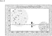
FIG. 2 is a graph showing the correlation between welding strength and resistance. -
FIG. 3 is a normal distribution curve of resistance values of a sample group according to an embodiment of the present invention. -
FIG. 4 is a schematic diagram showing a method of measuring a resistance according to an embodiment of the present invention. -
FIG. 5 is a schematic diagram showing a method of measuring a resistance according to another embodiment of the present invention. -
FIG. 6 is a schematic diagram of a resistance measuring probe of the present invention. -
FIG. 7 is a schematic diagram showing a method of measuring a resistance of a welded portion by ultrasonic welding according to an embodiment of the present invention. -
FIG. 8 is a schematic diagram showing a method of measuring a resistance of a welded portion by laser welding according to an embodiment of the present invention. - Hereinafter, preferred embodiments of the present invention will be described in detail with reference to the accompanying drawings. The terms and words used in the present specification and claims should not be construed as limited to ordinary or dictionary terms and the inventor may properly define the concept of the terms in order to best describe its invention. The terms and words should be construed as meaning and concept consistent with the technical idea of the present invention.
- Accordingly, the embodiments described in the specification and the configurations described in the drawings are only the most preferred embodiments of the present invention, and do not represent all of the technical ideas of the present invention. It is to be understood that there may be various equivalents and variations in place of them at the time of filing the present application.
- Also, throughout the specification, when an element is referred to as "including" an element, it is understood that the element may include other elements as well unless specifically stated otherwise.
-
FIG. 1 is a flowchart of a method for inspecting a welding defect according to the present invention. Referring toFIG. 1 , a method for inspecting a welding defect of the present invention includes: a threshold resistance setting step (S100) of measuring a resistance of a welded portion of a sample group and deriving a threshold resistance value which becomes an evaluation standard of a weak welding; a resistance measuring step (S200) of measuring a resistance value of a welded portion to be inspected; and a determination step (S300) of determining the welded portion as a weak welding if the resistance value measured in the resistance measuring step exceeds the threshold resistance value, wherein the threshold resistance setting step (S100) and the resistance measuring step (S200) include measuring a resistance using a microresistance measuring instrument having a resolution of nanoohm to microohm units. - The inventors of the present invention have found that the electric resistance value of the welded portion having a low welding strength was greater than the electric resistance value of the welded portion having a normal welding strength, which has led them to the present invention. Referring to
FIG. 2 , a resistance value of a welded portion having been welded by a normal welding strength of 22 kgf or more is smaller than a resistance value of a welded portion having been welded by a weak welding strength less than 22 kgf. Conventionally, there was a technology of inspecting a welding defect by measuring the resistance of the welded portion and comparing the measured resistance value with the threshold resistance value. However, in the conventional technology, the method of deriving the threshold resistance value was not specific, or a process of measuring the tensile strength of the welded portion was necessary because the correlation between the tensile strength of the welded portion and the resistance was used when deriving the threshold resistance value. - However, the present invention is characterized in introducing a statistical scheme in deriving a threshold resistance value while not relying on a correlation between a tensile strength and a resistance of a welded portion and in precisely measuring a resistance by measuring the resistance up to nanoohm to microohm levels by increasing the resolution.
- Namely, when the resistances for objects forming a large amount of sample groups are measured, the measured resistance values form a normal distribution curve. In the normal distribution curve, an object having a large deviation may be easily assumed as being defective from a standpoint of a statistical probability, and thus a predetermined deviation is determined as a threshold resistance value. Further, this approach is based on a premise that data for the sample group are reliable. Hence, a microresistance measuring instrument capable of precisely measuring the resistance up to nanoohm to microohm levels for the sample group is used in the process of setting a threshold value, and a microresistance measuring instrument capable of precisely measuring the resistance up to nanoohm to microohm levels is used when measuring the resistance for the object to be inspected. Likewise, in the present invention, a threshold resistance value is statistically derived from a large amount of sample groups when deriving the threshold resistance value. Hence, it is not necessary to separately measure the tensile strength of the welded portion in order to set the threshold resistance value unlike the conventional technology.
- First, the threshold resistance setting step (S100) will be described.
- The threshold resistance setting step (S100) according to an embodiment of the present invention includes: a data construction step (S 110) of measuring a microresistance of nanoohm and microohm units for a sample group and storing the measured microresistance; and a threshold resistance value deriving step (S120) of deriving a threshold value by processing data accumulated by the data construction step (S110) by a statistical scheme.
- The data construction step (S110) includes a process of measuring the resistance of a welded portion for objects which form a sample group. At this time, the number of objects of the sample group is at least 100,000, preferably 200,000, and it is preferable to have as many objects of the sample group as possible in terms of reliability.
- In the data construction step (S110), resistances for objects of the sample group are measured by using a microresistance measuring instrument having a resolution of nanoohm (nΩ) to microohm (uΩ) units. This is to accumulate more reliable data. Further, the microresistance measuring method is performed in the same manner as that of the scheme of measuring the resistance of the welded portion in the resistance measuring step (S200).
- The threshold resistance value deriving step (S120) includes deriving a threshold resistance value by processing data accumulated by the data construction step (S I 10) by a statistical scheme. The statistical processing method according to an embodiment of the present invention is to obtain a normal distribution curve of the resistance value of an object of the sample group and to the + 6δ value in the normal distribution curve as the threshold resistance value.
-
FIG. 3 shows an example of a distribution curve of resistances of a sample group according to an embodiment of the present invention. Referring toFIG. 3 , when the sample group shows a normal distribution curve as inFIG. 3 , the majority of objects have values close to the average value (µ), and the number of objects having a value, which is significantly deviated from the average value (µ), is small. Therefore, objects having a value, which is significantly deviated from the average value, may be stochastically assumed as being defective. Specifically, the probability that an object having a deviation of 1δ (standard deviation) appears is about 32%, the probability that an object having a deviation of 2δ appears is about 5%, the probability that an object having a deviation of 3δ appears is about 0.3%, the probability that an object having a deviation of 4δ appears is about 0.01%, the probability that an object having a deviation of 5δ appears is about 0.001%, and the probability that an object having a deviation of 6δ appears is about 0.0000001%. - As such, in an embodiment of the present invention, the sum of the average value and 6δ was set as the threshold resistance value.
- Hereinafter, the resistance measuring step (S200) will be described in detail.
-
FIG. 4 is a schematic diagram showing a method of measuring a resistance according to an embodiment of the present invention. Referring toFIG. 4 , a microresistance measuring instrument, which is used for resistance measurement in the resistance measuring step (S200) of the present invention, includes tworesistance measuring probes 100, and resistances are measured by allowing the two resistance measuring probes to contact the weldedportion 30. - The resistance of the entire welded
portion 30 can be measured by allowing one resistance measuring probe to contact oneend 31 of the welded portion and allowing the other resistance measuring probe to contact the other end of the welded portion. - Further, as illustrated in
FIG. 4(b) , the weldedportion 30 can be divided into a weldedportion 33 of theelectrode tab 20 portion and a weldedportion 34 of theelectrode lead 10, and as illustrated inFIG. 4(b) , both of the two resistance measuring probes can be allowed to contact the weldedportion 33 of theelectrode tab 20. Unlike this, both of the two resistance measuring probes may be allowed to contact the weldedportion 34 of theelectrode lead 10. Alternatively, as illustrated inFIG. 5 , one resistance measuring probe may be allowed to contact the weldedportion 33 of theelectrode tab 20, and the remaining one resistance measuring probe may be allowed to contact the weldedportion 34 of theelectrode lead 10, to thereby measure the resistance. Among the above embodiments, it was most preferable to measure the resistance in the form of contacting both of the two resistance measuring probes on the weldedportion 33 of theelectrode tab 10 in terms of the detection power of detecting a weak welding. -
FIG. 6 shows a schematic diagram of a resistance measuring probe of the present invention, and referring toFIG. 6 , theresistance measuring probe 100 of the present invention includes acurrent probe 110 and avoltage probe 120. The current probe applies current to a welded portion to be measured, and the voltage probe measures voltages. As such, the resistance of the welded portion can be measured. - In the present invention, the resistance is measured by allowing two resistance measuring probes to contact the welded portion. As such, the resistance of the welded portion can be measured by a 4-wire type measuring scheme. Since the 4-wire type resistance measuring scheme is less influenced by the contact resistance compared to the 2-wire type resistance measuring scheme, the microresistance can be more precisely measured in the 4-wire type resistance measuring scheme, in which the resistance can be measured even in nanoohm units.
- In one specific example, the resistance measuring step (S200) includes measuring a resistance of a welded portion by a direct current scheme. The direct current scheme has an advantage that high-precision resistance measurement is possible, compared to the alternating current scheme.
- The welding defect inspection method of the present invention can be widely applied to the welded portion of the secondary battery and can be applied to the welded portion according to various welding schemes. Namely, the welding defect inspection method of the present invention can be applied to a welded portion between an electrode tab and an electrode tab, a welded portion between an electrode tab and an electrode lead, and a welded portion between an electrode lead and a bus bar in a battery pack, and may also be applied to a welded portion by ultrasonic welding and a welded portion by laser welding, etc.
-
FIG. 7 is a schematic diagram showing a method of measuring a resistance to a welded portion according to an ultrasonic welding scheme. Referring toFIG. 7 , a weldedportion 30 formed by the ultrasonic welding scheme has the form of a line or a surface. As such, thecontact position 40 of the resistance measuring probe for resistance measurement is positioned on the boundary line of the welded portion. The resistance of the entire welded portion can be measured by allowing the resistance measuring probe to contact the boundary line of the welded portion. There are 4contact positions 40 of the resistance measuring probe. Herein, the current probe contacts two of the contact positions 40, and the voltage probe contacts the remaining two of the contact positions 40. -
FIG. 8 is a schematic diagram showing a method of measuring a resistance to a welding portion according to a laser welding scheme. Referring toFIG. 8 , the weldedportion 30 formed by the laser welding scheme has a dotted shape. In order to measure the resistance of the entire welded portion, it is desirable to determine thecontact position 40 of the resistance measuring probe on the outer peripheral surface with a virtual line obtained by connecting points at the outermost portions of the points as the boundary. There are 4contact positions 40 of the resistance measuring probe. Herein, the current probe contacts two of the contact positions 40, and the voltage probe contacts the remaining two of the contact positions 40. - According to the welding inspection method of the present invention, resistances of a sample group are measured, a threshold resistance value is set from a normal distribution curve of the measured resistance values, and resistances are precisely measured by using a microresistance measuring instrument having a resolution of nanoohm to microohm levels when measuring resistances for the sample group and the welded portion to be inspected, thereby showing an excellent detection power for a weak welding defect.
Claims (15)
- A method for inspecting a welding defect, comprising:a threshold resistance setting step (S100) of measuring a resistance of a welded portion of a sample group and deriving a threshold resistance value which becomes an evaluation standard of a weak welding;a resistance measuring step (S200) of measuring a resistance value of a welded portion to be inspected; anda determination step (S300) of determining the welded portion as a weak welding if the resistance value measured in the resistance measuring step exceeds the threshold resistance value,wherein the threshold resistance setting step (S100) and the resistance measuring step (S200) include measuring a resistance using a microresistance measuring instrument having a resolution of nanoohm to microohm units.
- The method of claim 1, wherein the resistance measuring step (S200) includes measuring a resistance by allowing two resistance measuring probes to contact the welded portion.
- The method of claim 2, further comprising: measuring a total resistance of the welded portion by allowing one resistance measuring probe to contact one end of the welded portion and allowing another resistance measuring probe to contact an other end of the welded portion.
- The method of claim 2, wherein the resistance measuring probe includes a voltage probe and a current probe.
- The method of claim 1, wherein the resistance measuring step (S200) includes measuring a resistance of the welded portion by a 4-wire type measuring scheme.
- The method of claim 1, wherein the resistance measuring step (S200) includes measuring a resistance of the welded portion by a direct current scheme.
- The method of claim 1, wherein the threshold resistance setting step (S100) comprises:a data construction step (S110) of measuring a microresistance of nanoohm and microohm units for the sample group and storing the measured microresistance; anda threshold resistance value deriving step (S120) of deriving the threshold resistance value by processing data accumulated by the data construction step (S110) by a statistical scheme.
- The method of claim 7, wherein a number of objects of the sample group is equal to or greater than 100,000.
- The method of claim 7, wherein resistance values of the sample group form a normal distribution curve.
- The method of claim 9, wherein the threshold resistance value is an average value + 6δ.
- The method of claim 3, wherein the welded portion is formed by a ultrasonic welding.
- The method of claim 11, wherein the resistance is measured by allowing the resistance measuring probe to contact a boundary line of the welded portion.
- The method of claim 3, wherein the welded portion is formed by a laser welding.
- The method of claim 13, wherein the resistance is measured by allowing the resistance measuring probe to contact an outer peripheral surface of the welded portion.
- The method of claim 1, wherein the welded portion is one selected from a welded portion between an electrode lead and an electrode tab of a pouch-type secondary battery, and a welded portion between an electrode tab and an electrode tab of a pouch-type secondary battery.
Applications Claiming Priority (2)
| Application Number | Priority Date | Filing Date | Title |
|---|---|---|---|
| KR1020200023657A KR102772444B1 (en) | 2020-02-26 | 2020-02-26 | A detecting method of welding defect |
| PCT/KR2020/019247 WO2021172728A1 (en) | 2020-02-26 | 2020-12-29 | Welding failure inspection method |
Publications (3)
| Publication Number | Publication Date |
|---|---|
| EP4032655A1 true EP4032655A1 (en) | 2022-07-27 |
| EP4032655A4 EP4032655A4 (en) | 2022-12-07 |
| EP4032655B1 EP4032655B1 (en) | 2024-09-11 |
Family
ID=77491292
Family Applications (1)
| Application Number | Title | Priority Date | Filing Date |
|---|---|---|---|
| EP20921672.0A Active EP4032655B1 (en) | 2020-02-26 | 2020-12-29 | Welding failure inspection method |
Country Status (9)
| Country | Link |
|---|---|
| US (1) | US12025578B2 (en) |
| EP (1) | EP4032655B1 (en) |
| JP (1) | JP7479465B2 (en) |
| KR (1) | KR102772444B1 (en) |
| CN (1) | CN114616462B (en) |
| ES (1) | ES2996905T3 (en) |
| HU (1) | HUE068983T2 (en) |
| PL (1) | PL4032655T3 (en) |
| WO (1) | WO2021172728A1 (en) |
Families Citing this family (2)
| Publication number | Priority date | Publication date | Assignee | Title |
|---|---|---|---|---|
| CN119846494A (en) * | 2023-10-18 | 2025-04-18 | 宁德时代新能源科技股份有限公司 | Battery busbar testing device, method and system, electronic equipment and medium |
| KR20260011368A (en) | 2024-07-16 | 2026-01-23 | 주식회사 엘지에너지솔루션 | Laser welding apparatus and method |
Family Cites Families (23)
| Publication number | Priority date | Publication date | Assignee | Title |
|---|---|---|---|---|
| JP2000100465A (en) | 1998-09-25 | 2000-04-07 | Fuji Photo Film Co Ltd | Check device and checking method for battery |
| JP4330690B2 (en) | 1999-03-16 | 2009-09-16 | パナソニック株式会社 | Detection method of defective welding of secondary battery |
| US6265688B1 (en) | 2000-02-03 | 2001-07-24 | Norman A. Lyshkow | Method of welding metals and apparatus for use therefor |
| JP4474808B2 (en) | 2001-06-28 | 2010-06-09 | 株式会社デンソー | Nondestructive inspection method for welded parts and nondestructive inspection apparatus for welded parts |
| US7988745B2 (en) | 2006-02-07 | 2011-08-02 | Gs Yuasa International Ltd. | Method for manufacturing battery, battery manufactured by the method, and method for inspecting battery |
| KR100886572B1 (en) | 2006-02-13 | 2009-03-05 | 주식회사 엘지화학 | How to check the welding condition of the unit cells in the middle- or large-sized battery module |
| US8406504B2 (en) * | 2007-11-02 | 2013-03-26 | Nippon Steel & Sumitomo Metal Corporation | System and method for monitoring of welding state |
| JP5127788B2 (en) * | 2009-08-01 | 2013-01-23 | 株式会社豊田中央研究所 | Resistance welding method, resistance welding member, resistance welding machine, resistance welding machine control method and control program and control device thereof, resistance welding evaluation method and evaluation program and evaluation device thereof |
| US8421472B2 (en) * | 2010-03-11 | 2013-04-16 | Toyota Motor Engineering & Manufacturing North America, Inc. | Apparatuses and methods for testing welding apparatuses |
| JP2012200765A (en) | 2011-03-25 | 2012-10-22 | Toyota Motor Corp | Method and device for evaluating quality of resistance welding |
| US9421634B2 (en) * | 2011-11-09 | 2016-08-23 | Fca Us Llc | System and method for performing resistance spot welding |
| KR101487577B1 (en) * | 2012-02-02 | 2015-01-29 | 주식회사 엘지화학 | Method and apparatus for detecting default of battery pack, and power relay assembly thereof |
| KR20130097990A (en) | 2012-02-27 | 2013-09-04 | 조선대학교산학협력단 | T-joint welding method for pole rod and tap of secondary battery |
| CN103376278B (en) * | 2012-04-27 | 2016-03-16 | 协鑫动力新材料(盐城)有限公司 | A kind of method detecting lithium ion battery tab welding firmness |
| KR20140141289A (en) | 2013-05-31 | 2014-12-10 | 주식회사 엘지화학 | Finding method of welding error for parallel-tap |
| US9843002B2 (en) | 2015-10-29 | 2017-12-12 | Semiconductor Energy Laboratory Co., Ltd. | Organometallic complex, light-emitting element, light-emitting device, electronic device, and lighting device |
| US10274448B2 (en) | 2016-05-06 | 2019-04-30 | GM Global Technology Operations LLC | Method and apparatus for evaluating a weld junction between a terminal and an electrode element of a battery cell |
| CN107607592A (en) | 2017-10-10 | 2018-01-19 | 深圳军洋科技发展有限公司 | Soldering reliability method of testing and equipment |
| KR101887148B1 (en) | 2017-12-22 | 2018-08-09 | 조태문 | System and Apparatus for Inspecting Weld Quality |
| CN108181356A (en) * | 2018-01-11 | 2018-06-19 | 哈尔滨理工大学 | A method for measuring battery welding quality |
| KR102057781B1 (en) | 2018-06-25 | 2019-12-19 | 현대제철 주식회사 | Apparatus and method for quality prediction of spot welds |
| KR102173204B1 (en) | 2018-08-13 | 2020-11-03 | 고려대학교 산학협력단 | System and method for analyzing patent based on visualizing big data |
| US11906593B2 (en) * | 2019-10-31 | 2024-02-20 | Keysight Technologies, Inc. | Method and system for testing the structural integrity of a metal joint |
-
2020
- 2020-02-26 KR KR1020200023657A patent/KR102772444B1/en active Active
- 2020-12-29 ES ES20921672T patent/ES2996905T3/en active Active
- 2020-12-29 PL PL20921672.0T patent/PL4032655T3/en unknown
- 2020-12-29 CN CN202080075215.3A patent/CN114616462B/en active Active
- 2020-12-29 US US17/771,163 patent/US12025578B2/en active Active
- 2020-12-29 WO PCT/KR2020/019247 patent/WO2021172728A1/en not_active Ceased
- 2020-12-29 HU HUE20921672A patent/HUE068983T2/en unknown
- 2020-12-29 JP JP2022524016A patent/JP7479465B2/en active Active
- 2020-12-29 EP EP20921672.0A patent/EP4032655B1/en active Active
Also Published As
| Publication number | Publication date |
|---|---|
| KR20210108716A (en) | 2021-09-03 |
| ES2996905T3 (en) | 2025-02-13 |
| JP2023500225A (en) | 2023-01-05 |
| PL4032655T3 (en) | 2025-01-20 |
| US20220412911A1 (en) | 2022-12-29 |
| EP4032655B1 (en) | 2024-09-11 |
| JP7479465B2 (en) | 2024-05-08 |
| EP4032655A4 (en) | 2022-12-07 |
| HUE068983T2 (en) | 2025-02-28 |
| CN114616462A (en) | 2022-06-10 |
| KR102772444B1 (en) | 2025-02-25 |
| US12025578B2 (en) | 2024-07-02 |
| CN114616462B (en) | 2025-07-01 |
| WO2021172728A1 (en) | 2021-09-02 |
Similar Documents
| Publication | Publication Date | Title |
|---|---|---|
| EP4026651B1 (en) | Welding quality inspection device | |
| US9354278B2 (en) | Device for detecting normal, abnormal or deteriorated battery state | |
| JP2023514285A (en) | Battery system diagnosis device and method | |
| US20220399587A1 (en) | Battery Pack Having Improved Swelling Measurement Accuracy | |
| KR102886237B1 (en) | Method for detecting abnormal battery through relative comparison | |
| EP4203141B1 (en) | Battery system diagnosing apparatus and method | |
| EP3995844A1 (en) | Battery defect screening device and method | |
| EP4032655B1 (en) | Welding failure inspection method | |
| US11598814B2 (en) | Battery management apparatus and method | |
| EP4254719B1 (en) | Method for determining charging profile of battery and battery charging system using same | |
| US11680990B2 (en) | System and method for estimating state of health of all-solid-state battery | |
| KR102872285B1 (en) | Detectign appratus and method of welding defect | |
| US12569938B2 (en) | Device and method for inspecting welded state | |
| KR20230032724A (en) | Apparatus and method for detecting internal defects of battery cell using tdr | |
| CN117083146A (en) | Device and method for checking welding status |
Legal Events
| Date | Code | Title | Description |
|---|---|---|---|
| STAA | Information on the status of an ep patent application or granted ep patent |
Free format text: STATUS: THE INTERNATIONAL PUBLICATION HAS BEEN MADE |
|
| PUAI | Public reference made under article 153(3) epc to a published international application that has entered the european phase |
Free format text: ORIGINAL CODE: 0009012 |
|
| STAA | Information on the status of an ep patent application or granted ep patent |
Free format text: STATUS: REQUEST FOR EXAMINATION WAS MADE |
|
| 17P | Request for examination filed |
Effective date: 20220419 |
|
| AK | Designated contracting states |
Kind code of ref document: A1 Designated state(s): AL AT BE BG CH CY CZ DE DK EE ES FI FR GB GR HR HU IE IS IT LI LT LU LV MC MK MT NL NO PL PT RO RS SE SI SK SM TR |
|
| A4 | Supplementary search report drawn up and despatched |
Effective date: 20221107 |
|
| RIC1 | Information provided on ipc code assigned before grant |
Ipc: G01N 33/207 20190101ALI20221031BHEP Ipc: G01N 27/20 20060101ALI20221031BHEP Ipc: H01M 50/531 20210101ALI20221031BHEP Ipc: B23K 11/25 20060101ALI20221031BHEP Ipc: B23K 31/12 20060101AFI20221031BHEP |
|
| DAV | Request for validation of the european patent (deleted) | ||
| DAX | Request for extension of the european patent (deleted) | ||
| STAA | Information on the status of an ep patent application or granted ep patent |
Free format text: STATUS: EXAMINATION IS IN PROGRESS |
|
| 17Q | First examination report despatched |
Effective date: 20230823 |
|
| GRAP | Despatch of communication of intention to grant a patent |
Free format text: ORIGINAL CODE: EPIDOSNIGR1 |
|
| STAA | Information on the status of an ep patent application or granted ep patent |
Free format text: STATUS: GRANT OF PATENT IS INTENDED |
|
| GRAS | Grant fee paid |
Free format text: ORIGINAL CODE: EPIDOSNIGR3 |
|
| INTG | Intention to grant announced |
Effective date: 20240711 |
|
| GRAA | (expected) grant |
Free format text: ORIGINAL CODE: 0009210 |
|
| STAA | Information on the status of an ep patent application or granted ep patent |
Free format text: STATUS: THE PATENT HAS BEEN GRANTED |
|
| P01 | Opt-out of the competence of the unified patent court (upc) registered |
Free format text: CASE NUMBER: APP_44315/2024 Effective date: 20240730 |
|
| AK | Designated contracting states |
Kind code of ref document: B1 Designated state(s): AL AT BE BG CH CY CZ DE DK EE ES FI FR GB GR HR HU IE IS IT LI LT LU LV MC MK MT NL NO PL PT RO RS SE SI SK SM TR |
|
| REG | Reference to a national code |
Ref country code: GB Ref legal event code: FG4D |
|
| REG | Reference to a national code |
Ref country code: CH Ref legal event code: EP |
|
| REG | Reference to a national code |
Ref country code: DE Ref legal event code: R096 Ref document number: 602020037740 Country of ref document: DE |
|
| REG | Reference to a national code |
Ref country code: IE Ref legal event code: FG4D |
|
| REG | Reference to a national code |
Ref country code: NL Ref legal event code: FP |
|
| REG | Reference to a national code |
Ref country code: SE Ref legal event code: TRGR |
|
| REG | Reference to a national code |
Ref country code: LT Ref legal event code: MG9D |
|
| PG25 | Lapsed in a contracting state [announced via postgrant information from national office to epo] |
Ref country code: NO Free format text: LAPSE BECAUSE OF FAILURE TO SUBMIT A TRANSLATION OF THE DESCRIPTION OR TO PAY THE FEE WITHIN THE PRESCRIBED TIME-LIMIT Effective date: 20241211 |
|
| PG25 | Lapsed in a contracting state [announced via postgrant information from national office to epo] |
Ref country code: GR Free format text: LAPSE BECAUSE OF FAILURE TO SUBMIT A TRANSLATION OF THE DESCRIPTION OR TO PAY THE FEE WITHIN THE PRESCRIBED TIME-LIMIT Effective date: 20241212 Ref country code: FI Free format text: LAPSE BECAUSE OF FAILURE TO SUBMIT A TRANSLATION OF THE DESCRIPTION OR TO PAY THE FEE WITHIN THE PRESCRIBED TIME-LIMIT Effective date: 20240911 |
|
| PG25 | Lapsed in a contracting state [announced via postgrant information from national office to epo] |
Ref country code: BG Free format text: LAPSE BECAUSE OF FAILURE TO SUBMIT A TRANSLATION OF THE DESCRIPTION OR TO PAY THE FEE WITHIN THE PRESCRIBED TIME-LIMIT Effective date: 20240911 |
|
| PG25 | Lapsed in a contracting state [announced via postgrant information from national office to epo] |
Ref country code: LV Free format text: LAPSE BECAUSE OF FAILURE TO SUBMIT A TRANSLATION OF THE DESCRIPTION OR TO PAY THE FEE WITHIN THE PRESCRIBED TIME-LIMIT Effective date: 20240911 |
|
| PG25 | Lapsed in a contracting state [announced via postgrant information from national office to epo] |
Ref country code: HR Free format text: LAPSE BECAUSE OF FAILURE TO SUBMIT A TRANSLATION OF THE DESCRIPTION OR TO PAY THE FEE WITHIN THE PRESCRIBED TIME-LIMIT Effective date: 20240911 |
|
| PG25 | Lapsed in a contracting state [announced via postgrant information from national office to epo] |
Ref country code: RS Free format text: LAPSE BECAUSE OF FAILURE TO SUBMIT A TRANSLATION OF THE DESCRIPTION OR TO PAY THE FEE WITHIN THE PRESCRIBED TIME-LIMIT Effective date: 20241211 |
|
| PG25 | Lapsed in a contracting state [announced via postgrant information from national office to epo] |
Ref country code: RS Free format text: LAPSE BECAUSE OF FAILURE TO SUBMIT A TRANSLATION OF THE DESCRIPTION OR TO PAY THE FEE WITHIN THE PRESCRIBED TIME-LIMIT Effective date: 20241211 Ref country code: NO Free format text: LAPSE BECAUSE OF FAILURE TO SUBMIT A TRANSLATION OF THE DESCRIPTION OR TO PAY THE FEE WITHIN THE PRESCRIBED TIME-LIMIT Effective date: 20241211 Ref country code: LV Free format text: LAPSE BECAUSE OF FAILURE TO SUBMIT A TRANSLATION OF THE DESCRIPTION OR TO PAY THE FEE WITHIN THE PRESCRIBED TIME-LIMIT Effective date: 20240911 Ref country code: HR Free format text: LAPSE BECAUSE OF FAILURE TO SUBMIT A TRANSLATION OF THE DESCRIPTION OR TO PAY THE FEE WITHIN THE PRESCRIBED TIME-LIMIT Effective date: 20240911 Ref country code: GR Free format text: LAPSE BECAUSE OF FAILURE TO SUBMIT A TRANSLATION OF THE DESCRIPTION OR TO PAY THE FEE WITHIN THE PRESCRIBED TIME-LIMIT Effective date: 20241212 Ref country code: FI Free format text: LAPSE BECAUSE OF FAILURE TO SUBMIT A TRANSLATION OF THE DESCRIPTION OR TO PAY THE FEE WITHIN THE PRESCRIBED TIME-LIMIT Effective date: 20240911 Ref country code: BG Free format text: LAPSE BECAUSE OF FAILURE TO SUBMIT A TRANSLATION OF THE DESCRIPTION OR TO PAY THE FEE WITHIN THE PRESCRIBED TIME-LIMIT Effective date: 20240911 |
|
| REG | Reference to a national code |
Ref country code: ES Ref legal event code: FG2A Ref document number: 2996905 Country of ref document: ES Kind code of ref document: T3 Effective date: 20250213 |
|
| REG | Reference to a national code |
Ref country code: AT Ref legal event code: MK05 Ref document number: 1722275 Country of ref document: AT Kind code of ref document: T Effective date: 20240911 |
|
| REG | Reference to a national code |
Ref country code: HU Ref legal event code: AG4A Ref document number: E068983 Country of ref document: HU |
|
| PG25 | Lapsed in a contracting state [announced via postgrant information from national office to epo] |
Ref country code: PT Free format text: LAPSE BECAUSE OF FAILURE TO SUBMIT A TRANSLATION OF THE DESCRIPTION OR TO PAY THE FEE WITHIN THE PRESCRIBED TIME-LIMIT Effective date: 20250113 Ref country code: IS Free format text: LAPSE BECAUSE OF FAILURE TO SUBMIT A TRANSLATION OF THE DESCRIPTION OR TO PAY THE FEE WITHIN THE PRESCRIBED TIME-LIMIT Effective date: 20250111 |
|
| PG25 | Lapsed in a contracting state [announced via postgrant information from national office to epo] |
Ref country code: RO Free format text: LAPSE BECAUSE OF FAILURE TO SUBMIT A TRANSLATION OF THE DESCRIPTION OR TO PAY THE FEE WITHIN THE PRESCRIBED TIME-LIMIT Effective date: 20240911 Ref country code: SM Free format text: LAPSE BECAUSE OF FAILURE TO SUBMIT A TRANSLATION OF THE DESCRIPTION OR TO PAY THE FEE WITHIN THE PRESCRIBED TIME-LIMIT Effective date: 20240911 |
|
| PG25 | Lapsed in a contracting state [announced via postgrant information from national office to epo] |
Ref country code: AT Free format text: LAPSE BECAUSE OF FAILURE TO SUBMIT A TRANSLATION OF THE DESCRIPTION OR TO PAY THE FEE WITHIN THE PRESCRIBED TIME-LIMIT Effective date: 20240911 Ref country code: EE Free format text: LAPSE BECAUSE OF FAILURE TO SUBMIT A TRANSLATION OF THE DESCRIPTION OR TO PAY THE FEE WITHIN THE PRESCRIBED TIME-LIMIT Effective date: 20240911 |
|
| PG25 | Lapsed in a contracting state [announced via postgrant information from national office to epo] |
Ref country code: CZ Free format text: LAPSE BECAUSE OF FAILURE TO SUBMIT A TRANSLATION OF THE DESCRIPTION OR TO PAY THE FEE WITHIN THE PRESCRIBED TIME-LIMIT Effective date: 20240911 |
|
| PG25 | Lapsed in a contracting state [announced via postgrant information from national office to epo] |
Ref country code: SK Free format text: LAPSE BECAUSE OF FAILURE TO SUBMIT A TRANSLATION OF THE DESCRIPTION OR TO PAY THE FEE WITHIN THE PRESCRIBED TIME-LIMIT Effective date: 20240911 |
|
| REG | Reference to a national code |
Ref country code: DE Ref legal event code: R097 Ref document number: 602020037740 Country of ref document: DE |
|
| PG25 | Lapsed in a contracting state [announced via postgrant information from national office to epo] |
Ref country code: MC Free format text: LAPSE BECAUSE OF FAILURE TO SUBMIT A TRANSLATION OF THE DESCRIPTION OR TO PAY THE FEE WITHIN THE PRESCRIBED TIME-LIMIT Effective date: 20240911 |
|
| PG25 | Lapsed in a contracting state [announced via postgrant information from national office to epo] |
Ref country code: DK Free format text: LAPSE BECAUSE OF FAILURE TO SUBMIT A TRANSLATION OF THE DESCRIPTION OR TO PAY THE FEE WITHIN THE PRESCRIBED TIME-LIMIT Effective date: 20240911 |
|
| PLBE | No opposition filed within time limit |
Free format text: ORIGINAL CODE: 0009261 |
|
| STAA | Information on the status of an ep patent application or granted ep patent |
Free format text: STATUS: NO OPPOSITION FILED WITHIN TIME LIMIT |
|
| REG | Reference to a national code |
Ref country code: CH Ref legal event code: PL |
|
| PG25 | Lapsed in a contracting state [announced via postgrant information from national office to epo] |
Ref country code: LU Free format text: LAPSE BECAUSE OF NON-PAYMENT OF DUE FEES Effective date: 20241229 |
|
| 26N | No opposition filed |
Effective date: 20250612 |
|
| PG25 | Lapsed in a contracting state [announced via postgrant information from national office to epo] |
Ref country code: CH Free format text: LAPSE BECAUSE OF NON-PAYMENT OF DUE FEES Effective date: 20241231 |
|
| PG25 | Lapsed in a contracting state [announced via postgrant information from national office to epo] |
Ref country code: IE Free format text: LAPSE BECAUSE OF NON-PAYMENT OF DUE FEES Effective date: 20241229 |
|
| PGFP | Annual fee paid to national office [announced via postgrant information from national office to epo] |
Ref country code: NL Payment date: 20251120 Year of fee payment: 6 |
|
| PGFP | Annual fee paid to national office [announced via postgrant information from national office to epo] |
Ref country code: DE Payment date: 20251120 Year of fee payment: 6 |
|
| PGFP | Annual fee paid to national office [announced via postgrant information from national office to epo] |
Ref country code: GB Payment date: 20251120 Year of fee payment: 6 |
|
| PGFP | Annual fee paid to national office [announced via postgrant information from national office to epo] |
Ref country code: IT Payment date: 20251121 Year of fee payment: 6 |
|
| PGFP | Annual fee paid to national office [announced via postgrant information from national office to epo] |
Ref country code: HU Payment date: 20251216 Year of fee payment: 6 Ref country code: FR Payment date: 20251125 Year of fee payment: 6 |
|
| PGFP | Annual fee paid to national office [announced via postgrant information from national office to epo] |
Ref country code: TR Payment date: 20251125 Year of fee payment: 6 Ref country code: BE Payment date: 20251120 Year of fee payment: 6 |
|
| PGFP | Annual fee paid to national office [announced via postgrant information from national office to epo] |
Ref country code: SE Payment date: 20251121 Year of fee payment: 6 |
|
| PGFP | Annual fee paid to national office [announced via postgrant information from national office to epo] |
Ref country code: PL Payment date: 20251125 Year of fee payment: 6 |
|
| PGFP | Annual fee paid to national office [announced via postgrant information from national office to epo] |
Ref country code: ES Payment date: 20260122 Year of fee payment: 6 |