EP4032377B1 - Gerätegehäuse - Google Patents
Gerätegehäuse Download PDFInfo
- Publication number
- EP4032377B1 EP4032377B1 EP20771605.1A EP20771605A EP4032377B1 EP 4032377 B1 EP4032377 B1 EP 4032377B1 EP 20771605 A EP20771605 A EP 20771605A EP 4032377 B1 EP4032377 B1 EP 4032377B1
- Authority
- EP
- European Patent Office
- Prior art keywords
- enclosure
- equipment enclosure
- components
- channel
- housing
- Prior art date
- Legal status (The legal status is an assumption and is not a legal conclusion. Google has not performed a legal analysis and makes no representation as to the accuracy of the status listed.)
- Active
Links
Images


Classifications
-
- H—ELECTRICITY
- H05—ELECTRIC TECHNIQUES NOT OTHERWISE PROVIDED FOR
- H05K—PRINTED CIRCUITS; CASINGS OR CONSTRUCTIONAL DETAILS OF ELECTRIC APPARATUS; MANUFACTURE OF ASSEMBLAGES OF ELECTRICAL COMPONENTS
- H05K9/00—Screening of apparatus or components against electric or magnetic fields
- H05K9/0062—Structures of standardised dimensions, e.g. 19" rack, chassis for servers or telecommunications
-
- H—ELECTRICITY
- H05—ELECTRIC TECHNIQUES NOT OTHERWISE PROVIDED FOR
- H05K—PRINTED CIRCUITS; CASINGS OR CONSTRUCTIONAL DETAILS OF ELECTRIC APPARATUS; MANUFACTURE OF ASSEMBLAGES OF ELECTRICAL COMPONENTS
- H05K9/00—Screening of apparatus or components against electric or magnetic fields
- H05K9/0007—Casings
- H05K9/0009—Casings with provisions to reduce EMI leakage through the joining parts
-
- H—ELECTRICITY
- H05—ELECTRIC TECHNIQUES NOT OTHERWISE PROVIDED FOR
- H05K—PRINTED CIRCUITS; CASINGS OR CONSTRUCTIONAL DETAILS OF ELECTRIC APPARATUS; MANUFACTURE OF ASSEMBLAGES OF ELECTRICAL COMPONENTS
- H05K7/00—Constructional details common to different types of electric apparatus
- H05K7/02—Arrangements of circuit components or wiring on supporting structure
- H05K7/026—Multiple connections subassemblies
-
- H—ELECTRICITY
- H05—ELECTRIC TECHNIQUES NOT OTHERWISE PROVIDED FOR
- H05K—PRINTED CIRCUITS; CASINGS OR CONSTRUCTIONAL DETAILS OF ELECTRIC APPARATUS; MANUFACTURE OF ASSEMBLAGES OF ELECTRICAL COMPONENTS
- H05K9/00—Screening of apparatus or components against electric or magnetic fields
- H05K9/0007—Casings
- H05K9/0018—Casings with provisions to reduce aperture leakages in walls, e.g. terminals, connectors, cables
-
- H—ELECTRICITY
- H05—ELECTRIC TECHNIQUES NOT OTHERWISE PROVIDED FOR
- H05K—PRINTED CIRCUITS; CASINGS OR CONSTRUCTIONAL DETAILS OF ELECTRIC APPARATUS; MANUFACTURE OF ASSEMBLAGES OF ELECTRICAL COMPONENTS
- H05K9/00—Screening of apparatus or components against electric or magnetic fields
- H05K9/0073—Shielding materials
- H05K9/0081—Electromagnetic shielding materials, e.g. EMI, RFI shielding
- H05K9/0086—Electromagnetic shielding materials, e.g. EMI, RFI shielding comprising a single discontinuous metallic layer on an electrically insulating supporting structure, e.g. metal grid, perforated metal foil, film, aggregated flakes, sintering
Definitions
- the present invention concerns an equipment enclosure for electromagnetically isolating an electronic device, and in particular apparatus for housing an electronic device comprising a plurality of components.
- a typical electronic device such as a computing device will include a plurality of components, such as a router, a power source, a graphics card, a heat exchanger and a processor.
- EMSEC emissions security
- COMPEC communications security
- TEMPEST is a known shielding codename, which encompasses a collection of shielding techniques.
- TEMPEST shielding is concerned with the prevention of leaked electromagnetic signals and/or sound/mechanical vibrations.
- the device needs to be electromagnetically-isolated. This is usually achieved by placing the device in a Faraday cage that blocks electromagnetic fields that are radiating from the device. If the electronic device comprises a plurality of components, each component may require TEMPEST shielding, and may be individually isolated from electromagnetic radiation. The shielding used for the device or for each component of the device may result in the communications enclosure being large and heavy.
- each item shielded by a Faraday cage may be placed in a hermetically sealed box. Sealed boxes housing components of the communications device may be difficult to cool. Known mechanisms for cooling the components often require the use of air conditioning which adds further weight to the enclosure.
- US2016/205814 relates to a modular enclosure for electronics.
- US2012/262876 relates to a chassis for computing equipment.
- JP 2006 100419 relates to a shielded box for a printed circuit board.
- the present invention provides, according to a first aspect, an equipment enclosure according to claim 1.
- Optional features are set out in the dependent claims.
- the present invention provides an equipment enclosure for electromagnetically isolating an electronic device.
- the equipment enclosure comprises a conductive housing and a plurality of conductive sheets. Each sheet includes an aperture.
- the sheets are stacked in a spaced-apart relationship within the housing, thereby defining a plurality of electromagnetically-isolated cavities each within a respective Faraday cage formed by the conductive housing and the conductive sheets.
- the apertures form a channel that extends through the enclosure providing a route for connections between the cavities.
- Each conductive sheet may include two or more apertures.
- the apertures form two or more channels that extend through the enclosure, providing alternative routes for connections between the cavities.
- a structure for attenuating electromagnetic radiation originating from the electronic device may be provided in each of the channels.
- the structure may be a 3-dimensional cellular structure, and may comprise a plurality of cells.
- the cells may form sub-channels extending through the channel.
- the cellular structure may be a 3-dimensional honeycomb structure.
- the structure may be an aluminium honeycomb structure.
- the diameter of the channel may be at least 4 x the diameter of each of the cells.
- the diameter of the channel may be at least 6 x the diameter of each of the cells.
- the diameter of the cells that is required to attenuate electro-magnetic radiation depends upon the wavelength of the radiation, in accordance with well-known physical principals as discussed below.
- the effect of a cellular structure on electromagnetic radiation depends on the size of the cells and the wavelength of the radiation. If the diameter of the cells is very much larger than the wavelength of the electromagnetic radiation originating from the device, the radiation may not interact with the structure and therefore may not be attenuated. If the diameter of the cells is very much smaller than the wavelength of the electromagnetic radiation originating from the device, the radiation may not 'see' the cells and therefore may not be attenuated. If the diameter of the cells is comparable to the wavelength of the electro-magnetic radiation originating from the device, the radiation will be scattered by the cells, and the radiation tends to be attenuated by the structure.
- the efficiency of the structure at attenuating radiation may be dependent upon the ratio of the cell diameter to the wavelength of the radiation originating from the device.
- the diameter of the cells may be selected to be comparable to the wavelength of electromagnetic radiation originating from the device.
- the diameter of the cells may be the same order of magnitude as the wavelength of the radiation.
- the electronic device may generate electromagnetic radiation with a range of wavelengths.
- the range of wavelengths may be a distribution centered around a peak wavelength.
- the diameter of the cells may be selected such that cells attenuate radiation of the peak wavelength.
- the diameter of the cells may be smaller than the shortest wavelength of radiation emitted by the device.
- the structure may extend the entire length of the channel.
- the structure may be a sheet structure.
- the structure may extend partway along the length of the channel.
- the structure is relatively inefficient at attenuating the radiation from the device (for example, if the cells are significantly larger or smaller than the wavelength of the radiation, or if the radiation spans a wide range of wavelengths), a long structure may be required to ensure sufficient attenuation. If the structure is relatively efficient at attenuating radiation from the device (for example, if the cells are comparable in diameter to the wavelength of the radiation from the device), a shorter structure, for example, a sheet structure, may provide sufficient attenuation.
- the length of the sub-channels and therefore the length of the structure that is required to attenuate radiation generated by the device may also be dependent on the amplitude of the radiation. Longer sub-channels may be required to attenuate higher amplitude radiation. The length of the structure may therefore depend upon the amplitude of the radiation generated by the device.
- the cell diameter and length of the structure may be chosen such that electromagnetic radiation from the components is attenuated by the structure and is not transmitted between cavities.
- the sub-channels may allow air to pass through the channel.
- the sub-channels formed by the cells may be straight, curved or may comprise angled segments, such that zig-zag sub-channels are formed.
- the structure may be selected based on the device, the number of components of the device, and the wavelength and amplitude of radiation originating from the device.
- the conductive housing may comprise a cage or a box.
- the housing may comprise continuous sheets of conductive metal.
- the sheets should be sufficiently thick to absorb electromagnetic radiation originating from the device.
- the housing may comprise a wire mesh, providing that the apertures of the mesh are of a size that will block electromagnetic radiation from the device from passing through the housing and providing that the mesh is sufficiently thick to block radiation from passing through the housing, as explained above.
- the mesh may comprise conductive metal wire.
- the thickness of the sheet or the thickness of the mesh and size of the apertures may be selected depending on the device, the number of components of the device and the wavelength of radiation originating from the device.
- the equipment enclosure may house an electronic device comprising a plurality of components. Each component may be housed in a different electro-magnetically isolated cavity in the enclosure.
- the number of conducting sheets and therefore the number of electromagnetically-isolated cavities may be dependent on the number of components of the electronic device, or on the number of components that are required to be electromagnetically-isolated from each other.
- a communications enclosure with a suitable number of electromagnetically-isolated cavities may be selected.
- Each component may be housed in a separate cavity. More than one component may be housed in each cavity if these components do not need to be electromagnetically-isolated from each other.
- Each electromagnetically isolated cavity may comprise at least one additional sheet e.g. a non-conductive sheet that subdivides the cavity into two or more sub-cavities.
- the additional sheet may be stacked in a spaced-apart relationship between two conductive sheets, thereby dividing each cavity into at two sub-cavities.
- Components of the device that do not need to be electromagnetically isolated from one another may be housed in different sub-cavities within the same cavity.
- the volume and dimensions of the enclosure will be dependent upon the size, complexity and number of components of the electronic device.
- a suitably sized communications enclosure may be chosen.
- the size of enclosure may be chosen to avoid or minimise wasted space and excess weight.
- a typical enclosure may be between 0.012 and 0.015 m2 in volume, or between 0.014 and 0.015 m2 in volume.
- An enclosure may have dimensions of approximately 0.275 ⁇ 0.265 ⁇ 0.170 m.
- the enclosure may include mounting means for mounting the enclosure on a wall or other surface.
- the equipment enclosure may further comprise at least one external connector for providing a power supply to the electronic device.
- the external connector may connect at least one of the components of the electronic device to an external power supply.
- the external connector may be provided in an aperture in the enclosure housing.
- the equipment enclosure may further comprise at least one internal connector for providing an internal connection between electromagnetically-isolated components of the electronic device that are housed within the enclosure.
- the internal connector may pass through a channel in the enclosure and may connect at least two electro-magnetically-isolated components.
- any of the internal or external connectors may comprise a cable for coupling the components of the device or for coupling a component to an external power supply.
- the components of the electronic device may include connection ports for enabling connection to the internal and/or external connectors.
- the components may comprise internal connection ports for use with internal connectors and/or external connection ports for use with external connectors.
- Each cable may comprise a ribbon cable, a fibre optic cable or traditional cable such as a standard network cable.
- the connection terminal couples the cable to the component.
- the connection terminals may be USB ports or modified RJ45 terminals, such as spring loaded RJ45 terminals, which couple components via a cable.
- the internal connectors may comprise interslice bus connectors.
- Each interslice bus connector may comprise an interslice bus plug and an interslice socket for connecting components.
- Internal connectors may pass through a channel in the enclosure and may connect at least two electro-magnetically isolated components.
- External connectors may connect at least one component to an external power source, or to another external component via a connector that passes through an aperture in the enclosure housing.
- Components may be connected such that power can be transferred between the components.
- a component of the electronic device may receive power from an external power supply via an external connection, and this component may transfer power to other components of the device via an internal connection.
- Internal connectors may enable data to be transferred between components.
- Internal connectors may comprise power filters for transferring power between components.
- Components housed in different cavities may be isolated from each other unless connected by an internal connection.
- the equipment enclosure may include at least a first internal connector and a second internal connector.
- the different types of connector may provide different levels of shielding.
- the different types of connector may provide different levels of shielding from external/internal interference or from electromagnetic signals.
- the first internal connector may connect components that require a first level of shielding.
- the second internal connector may connect components that require a second, different level of shielding.
- a first connector type may provide complete shielding from external and/or internal interference.
- a second connector type may protect from external interference.
- the first internal connector may connect components via a cable that passes through a first channel in the enclosure.
- the second connector may connect components via a cable that passes through a second channel in the enclosure, or through the same first channel.
- Diagnostics may be checked by a user by interfacing with the internal or external connectors.
- Components requiring the same level of shielding may be connected by an internal connector, and these components may be isolated from other components requiring different levels of shielding. If a first component and a second component are housed in adjacent cavities and these components require different shielding levels, the second component may be bypassed from connection, and may either be a standalone component (i.e. not connected to any other components), or may be connected to another component in a different cavity that requires the same or a similar level of shielding.
- the electronic device may comprise a computing device.
- the computing device may include at least one of a crypto unit, a processor, a router, a power supply unit, a high performance EMI filter, and a circulator.
- the equipment enclosure may include a cooling mechanism for transferring heat away from the components of the device.
- the cooling mechanism may be any suitable cooling mechanism.
- the cooling mechanism may be a device that cools by convection, such as a fan.
- Each conductive sheet in the equipment enclosure may include a further aperture, and these apertures may form a cooling channel extending through the housing.
- a cooling device may be provided in the cooling channel.
- the cooling device may comprise a pressure vessel, wherein the pressure vessel comprises an evaporator proximate to a component.
- the cooling device may comprise a condenser end, and a working fluid provided within the pressure vessel.
- the working fluid may absorb heat at the evaporator, thereby generating a pressure gradient within the pressure vessel.
- the pressure gradient may cause the working fluid to away flow from the evaporator end towards the condenser end, thereby transferring heat away from the component.
- the cooling device may comprise a pressure vessel, a porous wick structure and a working fluid.
- the wick structure may be arranged on the inside of the vessel proximate to a heat-generating component of the device.
- the wick structure may be arranged at an end of the cooling device, and this end of the device may function as an evaporator.
- the working fluid vaporises, creating a pressure gradient.
- This pressure gradient pushes the vapour to flow along the device, through a central channel, to a condenser end.
- the condenser end may be proximate to a heat exchanger. At the condenser end, the vapour condenses due to this end being cooler, giving up its latent heat of vaporisation.
- the working fluid is then returned to the evaporator end by capillary forces developed in the wick structure or by gravity.
- the pressure vessel of the heat pipe may comprise a material having a high strength and high thermal conductivity such as copper or aluminium.
- the working fluid may comprise a fluid having high latent heat of vaporisation and high thermal conductivity.
- the working fluid may comprise a fluid having a latent heat of vaporisation greater than 800 kJ/kg or greater than 1000 kJ/kg.
- the working fluid may comprise a fluid having a thermal conductivity greater than 0.15 W/m ⁇ K or greater than 0.5 W/m ⁇ K at room temperature.
- the working fluid may comprise liquid helium, ammonia, or alcohol such as ethanol.
- the wick structure maintains efficient capillary action when bent or used against gravity.
- the wick structure may comprise, for example, sintered copper powder, a screen or a series of grooves parallel to the longitudinal axis of the cooling device.
- the evaporator end of the heat pipe may be proximate to a heat-generating component of the device.
- the opposite end (i.e. the condenser end) of the cooling device may be in proximity to at least one heat exchanger.
- the condenser end of the heat pipe is bifurcated such that one branch of the condenser end is disposed adjacent a first heat exchanger and another branch of the condenser end is disposed adjacent a second heat exchanger.
- a heat exchanger may be disposed on either side of the condenser end of the cooling device.
- the evaporator end of the cooling device may be bifurcated, or further divided to approach the heat-generating components of the device from different directions, or to allow a single cooling device to be used to transport heat away from a plurality of heat-generating components.
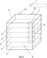
- an equipment enclosure 1 is provided for electromagnetically-isolating an electronic device.
- the enclosure comprises a conductive housing 3 and a plurality of conductive sheets 5.
- Each conductive sheet 5 includes an aperture 7.
- the sheets 5 are stacked in a spaced-apart relationship within the housing 3, thereby defining a plurality of electromagnetically-isolated cavities 9.
- Each cavity 9 is electromagnetically-isolated from adjacent cavities 9 and each cavity 9 is within a Faraday cage formed by the conductive housing 3 and the conductive sheets 5.
- the apertures 7 form a channel 11 that extends through the housing 3 (indicated by dashed lines in Figures 1 and 2 ).
- the enclosure 1 includes mounting means 12 (shown in Figure 2 ) for mounting the enclosure 1 on a wall or other surface.
- a 3-dimensional cellular honeycomb structure 308 is provided in a channel 311.
- the plurality of hexagonal cells 310 form sub-channels that extend through the channel 311.
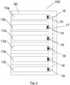
- the equipment enclosure 100 houses a computing device 13a-f.
- the computing device 13a-f comprises a plurality of components 13a-f.
- the components 13a-f are housed in the cavities 90 provided in the enclosure 100. Each component is housed in a different cavity. Each component 13a-f is electromagnetically-isolated from components in other cavities 90.
- the components include a crypto unit 13a, a power supply unit 13b, a high performance EMI filter 13c, a circulator 13d, a processor 13e, and a router 13f.
- the components 13a-f are connected by an internal connector 15 that passes through a channel.
- the connector comprises a cable 17 and a plurality of connection terminals 19.
- the enclosure 1000 comprises more than one internal connector 150a,b, c and d for providing connections between components 130a-f of the equipment device 130a-f.
- Connector 150a comprises a cable 170a and a connection terminal 190a/191a at each end of the cable 170a.
- the connection terminals 190a/191a couple to the components 130d and 130f.
- Connectors 150b, c and d comprise cables 170b, c, and d, connection terminals 190b/191b, 190c/191c, 190d/191d and 190e/191e at each end of the cables 170b, c and d.
- the connection terminals 190b, c and d couple to the components 130d and 130f.
- the connectors 150a and 150b/c/d pass through different channels 210a and 210b to connect the components.
- the connectors 150a, b, c and d are different types of connector and provide different levels of shielding.
- the connectors 150a, b, c and d may include different cable types 170a, b, c and d.
- connector 150a is a high shielding connector, which couples two of the processors 130d and 130f from both external and internal interference.
- Connector 150a bypasses the component 130e, as this component requires a different level of shielding.
- Connector 150b is a lower shielding connector and connects the component 130a to the component 130b.
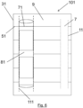
- the equipment enclosure 101 includes a cooling mechanism.
- Each conductive sheet 51 includes a second aperture 71, and these second apertures 71 form a second channel 111 extending through the housing 31.
- a cooling device 81 is disposed in the second channel 111 and provides cooling for the enclosure 101.
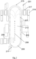
- FIG. 7 is a schematic view of an example cooling device 201 for use in the present invention.
- the cooling device comprises a pressure vessel 203, a porous wick structure 205 and a working fluid 207.
- the wick structure 205 is arranged on the inside of the vessel 203 proximate to a heat-generating component of the device 209.
- the wick structure 205 is arranged at an end 211 of the heat pipe 201 and this end 211 of the heat pipe 201 functions as an evaporator. Heat from the heat-generating component 209 is input at the evaporator end 211. This causes the working fluid 207 to vaporise, creating a pressure gradient.
- the pressure gradient pushes the vapour 208 to flow along the cooling device 201, through a central channel 213 to a condenser end 215.
- the condenser end 215 is proximate to a heat exchanger 217.
- the vapour 208 condenses due to this end being cooler, giving up its latent heat of vaporisation. Heat is transferred to the atmosphere 219 via the heat exchanger 217.
- the working fluid 207 is then returned to the evaporator end 211 by capillary forces developed in the wick structure 205 or by gravity.
- an equipment enclosure 401 for electromagnetically isolating an electronic device.
- the enclosure 401 comprises a conductive housing 403 and a plurality of conductive sheets 405.
- Each conductive sheet 405 includes an aperture 407.
- the sheets 405 are stacked in a spaced-apart relationship within the housing 403, thereby defining a plurality of electromagnetically isolated cavities 409.
- Each cavity 409 is electro-magnetically isolated from other cavities 409 and each cavity is within a Faraday cage formed by the conductive housing 403 and the conductive sheets 405.
- the equipment enclosure 401 houses a computing device 413.
- the computing device 413 comprises a plurality of components 413a/b, including a crypo unit 413a.
- the components 413a/b are housed in the cavities 409 provided in the enclosure 401.
- the enclosure 401 includes internal connectors for providing connections between components 413a/b of the computing device 413.
- the connectors comprise inter-slice plugs 415a and sockets 415b.
- the connectors pass through a channel 417 to provide a connection between the components 413a/b. Data can be transferred between components via the interslice buses.
- the enclosure 401 comprises an external connector 419 for providing power to the electronic device.
- the external connector 419 is provided in an aperture 421 in the enclosure housing.
- Internal connectors in the form of power filters 425 are provided to transfer power between components 413a/b.
- the enclosure 401 comprises a further external connector 427 for providing an external interface for the crypto unit 413a/b. This further external connector 427 is provided in an aperture 429 in the enclosure housing.
- the sheets are stacked vertically on top of each other.
- the conductive sheets may be stacked horizontally, or stacked at any other angle.
- the structure for attenuating radiation is a 3-dimensional honeycomb cellular structure, wherein the cells extend through the channel forming sub-channels.
- the structure may be a cellular structure comprising square, rectangular, circle, or any other shaped cells.
- the sub-channels are shown as extending the entire length of the channel, however, the sub-channels may not extend the entire length of the sub-channel. The depth of the sub-channels will depend on a range of factors including the wavelength of the electromagnetic radiation and the diameter of the cells.
- the sub-channels formed in Figure 2 are shown as being straight sub-channels, but the sub-channels may be angled, or may comprise angled-portions that are arranged to form zig-zag sub-channels.
- the cooling mechanism may comprise a higher pressure supply channel and a lower pressure exhaust channel, separated by a heat spreader plate.
- the higher pressure supply channel may be provided by a series of apertures provided in each sheet of the enclosure.
- the lower pressure exhaust channel may be provided by a further series apertures in each sheet of the enclosure.
- a heat spreader plate provided in a cavity of the enclosure may transfer heat from the higher pressure channel to the low pressure channel to cool the enclosure.
Landscapes
- Engineering & Computer Science (AREA)
- Microelectronics & Electronic Packaging (AREA)
- Physics & Mathematics (AREA)
- Electromagnetism (AREA)
- Shielding Devices Or Components To Electric Or Magnetic Fields (AREA)
Claims (13)
- Ausrüstungseinfassung (1, 100, 101, 401) zum elektromagnetischen Isolieren einer elektronischen Vorrichtung (13a-f, 130a-f, 413), wobei die Ausrüstungseinfassung umfasst:ein leitfähiges Gehäuse (3, 31); undeine Vielzahl von leitfähigen Blättern (5, 51), wobei jedes Blatt eine Öffnung (7) einschließt, wobei die Blätter in einer beabstandeten Beziehung innerhalb des Gehäuses gestapelt sind, wodurch eine Vielzahl von elektromagnetisch isolierten Hohlräumen (9, 90) definiert wird, jeder innerhalb eines jeweiligen Faradayschen Käfigs, der durch das leitfähige Gehäuse und die leitfähigen Blätter ausgebildet wird, und wobei die Öffnungen einen Kanal (11, 210a/b, 417) ausbilden, der sich durch die Einfassung erstreckt und einen Weg für Verbindungen zwischen den Hohlräumen bereitstellt,dadurch gekennzeichnet, dass:erste und zweite interne Verbinder (15, 150a-d, 415) durch den Kanal in der Einfassung zum Verbinden von mindestens zwei elektromagnetisch isolierten Komponenten verlaufen, undwobei der erste und der zweite Verbinder unterschiedliche Abschirmungsgrade bereitstellen und wobei der erste Verbinder Komponenten verbindet, die einen ersten Abschirmungsgrad erfordern, und der zweite Verbinder Komponenten verbindet, die einen zweiten, unterschiedlichen Abschirmungsgrad erfordern.
- Ausrüstungseinfassung nach Anspruch 1, wobei jedes leitfähige Blatt zwei oder mehr Öffnungen aufweist und wobei die Öffnungen zwei oder mehr Kanäle (11, 311) ausbilden, die sich durch die Einfassung erstrecken, wobei alternative Wege für Verbindungen zwischen den Hohlräumen bereitgestellt werden.
- Ausrüstungseinfassung nach einem der vorstehenden Ansprüche, wobei eine Struktur (308) zum Dämpfen elektromagnetischer Strahlung in jedem Kanal (311) bereitgestellt ist.
- Ausrüstungseinfassung nach Anspruch 3, wobei die Struktur eine 3-dimensionale Zellstruktur ist, umfassend eine Vielzahl von Zellen (310), die Unterkanäle ausbilden, die sich durch den Kanal erstrecken.
- Ausrüstungseinfassung nach Anspruch 4, wobei die Struktur eine 3-dimensionale Wabenstruktur ist.
- Ausrüstungseinfassung nach einem der vorstehenden Ansprüche, wobei die Einfassung eine elektronische Vorrichtung, umfassend mehrere Komponenten (413a/b, 13a-f, 130a-f), unterbringt und wobei jede Komponente in einem unterschiedlichen elektromagnetisch isolierten Hohlraum untergebracht ist.
- Ausrüstungseinfassung nach einem der vorstehenden Ansprüche, ferner umfassend mindestens einen externen Verbinder (419, 427) zum Bereitstellen von Leistung an die elektronische Vorrichtung.
- Ausrüstungseinfassung nach Anspruch 7, wobei der externe Verbinder mindestens eine Komponente der elektronischen Vorrichtung mit einer externen Leistungsversorgung verbindet und wobei der Verbinder in einer Öffnung (429) in dem Einfassungsgehäuse bereitgestellt ist.
- Ausrüstungseinfassung nach einem der vorstehenden Ansprüche, wobei die elektronische Vorrichtung eine Computervorrichtung umfasst, wobei die Computervorrichtung mindestens eines von einer Kryptoeinheit (13a, 413a/b), einem Prozessor (13e, 130d, 130f), einer Leistungsversorgungseinheit (13b), einem Hochleistungs-EMI-Filter (13c) und einem Zirkulator (13d) einschließt.
- Ausrüstungseinfassung nach einem der vorstehenden Ansprüche, ferner umfassend einen Kühlmechanismus (201).
- Ausrüstungseinfassung nach einem der vorstehenden Ansprüche, wobei jedes leitfähige Blatt eine weitere Öffnung (71) einschließt und wobei diese Öffnungen einen Kühlkanal ausbilden, der sich durch das Gehäuse erstreckt.
- Ausrüstungseinfassung nach Anspruch 11, wobei eine Kühlvorrichtung (201) in dem Kühlkanal (111) bereitgestellt ist.
- Ausrüstungseinfassung nach Anspruch 12, wobei die Kühlvorrichtung umfasst:ein Druckgefäß (203), wobei das Druckgefäß ein Verdampferende (211) in der Nähe zu einer Komponente (209) umfasst, das Verdampferende umfassend einen Verdampfer (205);ein Kondensatorende (215); undein Arbeitsfluid (207), das innerhalb des Druckgefäßes bereitgestellt ist,wobei das Arbeitsfluid (207) an dem Verdampfer Wärme aufnimmt und dadurch einen Druckgradienten innerhalb des Druckgefäßes erzeugt,und wobei der Druckgradient bewirkt, dass das Arbeitsfluid von dem Verdampferende zu dem Kondensatorende hin fließt, wodurch Wärme von der Komponente weggeleitet wird.
Applications Claiming Priority (3)
| Application Number | Priority Date | Filing Date | Title |
|---|---|---|---|
| GB1913445.1A GB2587212B (en) | 2019-09-18 | 2019-09-18 | Equipment enclosure |
| EP19275109.7A EP3817532A1 (de) | 2019-10-29 | 2019-10-29 | Gerätegehäuse |
| PCT/GB2020/052169 WO2021053319A1 (en) | 2019-09-18 | 2020-09-10 | Equipment enclosure |
Publications (3)
| Publication Number | Publication Date |
|---|---|
| EP4032377A1 EP4032377A1 (de) | 2022-07-27 |
| EP4032377C0 EP4032377C0 (de) | 2024-10-30 |
| EP4032377B1 true EP4032377B1 (de) | 2024-10-30 |
Family
ID=72473582
Family Applications (1)
| Application Number | Title | Priority Date | Filing Date |
|---|---|---|---|
| EP20771605.1A Active EP4032377B1 (de) | 2019-09-18 | 2020-09-10 | Gerätegehäuse |
Country Status (5)
| Country | Link |
|---|---|
| US (1) | US11582890B2 (de) |
| EP (1) | EP4032377B1 (de) |
| AU (1) | AU2020351296B2 (de) |
| CA (1) | CA3153852A1 (de) |
| WO (1) | WO2021053319A1 (de) |
Families Citing this family (2)
| Publication number | Priority date | Publication date | Assignee | Title |
|---|---|---|---|---|
| FR3143944A1 (fr) * | 2022-12-20 | 2024-06-21 | Sagemcom Broadband Sas | Boitier électronique comprenant des cartes électroniques |
| EP4654770A1 (de) * | 2024-05-20 | 2025-11-26 | Target Enclosure AB | Elektromagnetisch abgeschirmter elektronikkasten |
Citations (5)
| Publication number | Priority date | Publication date | Assignee | Title |
|---|---|---|---|---|
| US4370700A (en) * | 1980-06-03 | 1983-01-25 | Motorola Inc. | RF Package including RF shielding for a multiple PC board |
| CH654162A5 (de) * | 1981-07-24 | 1986-01-31 | Robert Doerig | Schutzraum fuer eine elektrische anlage. |
| CN105047648A (zh) * | 2015-06-23 | 2015-11-11 | 上海航天测控通信研究所 | 一种系统级封装结构及封装方法 |
| CN107275317A (zh) * | 2017-05-24 | 2017-10-20 | 中国电子科技集团公司第二十九研究所 | 一种薄膜陶瓷电路三维堆叠结构 |
| US20190326703A1 (en) * | 2018-04-18 | 2019-10-24 | Amphenol Corporation | High performance stacked connector |
Family Cites Families (22)
| Publication number | Priority date | Publication date | Assignee | Title |
|---|---|---|---|---|
| US3340439A (en) * | 1965-07-02 | 1967-09-05 | Amp Inc | Multi-contact connector |
| FI911185A7 (fi) * | 1991-03-08 | 1992-09-09 | Telenokia Oy | Arrangemang foer daempning av en genom anslutningsdon gaoende elektromagnetisk stoerning i en elektronisk anordning placerad inom ett ledande fodral |
| US5285007A (en) | 1992-02-03 | 1994-02-08 | Digital Equipment Corporation | System for reducing the emission of high frequency electromagnetic waves from computer systems |
| US5335144A (en) * | 1992-11-02 | 1994-08-02 | Samar Enterprises Company, Ltd. | Modular stacked housing arrangement |
| DE4407492A1 (de) | 1994-03-07 | 1995-09-14 | Bodenseewerk Geraetetech | Einrichtung zur Abschirmung von auf einer Elektronikkarte angeordneten elektronischen Bauteilen gegen äußere, elektromagnetische Felder |
| JP2006100419A (ja) | 2004-09-28 | 2006-04-13 | Canon Inc | プリント回路板ユニット |
| TWM378573U (en) * | 2009-09-15 | 2010-04-11 | Microelectronics Tech Inc | Low noise block converter |
| US9072169B1 (en) | 2010-07-13 | 2015-06-30 | Cascodium Inc. | Pulse generator and systems and methods for using same |
| US8614890B2 (en) * | 2011-04-18 | 2013-12-24 | Hewlett-Packard Development Company, L.P. | Chassis extension module |
| US9730339B2 (en) * | 2012-07-25 | 2017-08-08 | Edmund David Burke | Common bus structure for avionics and satellites (CBSAS) |
| US20160205814A1 (en) * | 2014-06-10 | 2016-07-14 | Space Information Laboratories - c/o Edmund Burke | Intelligent modular aerospace technology system (imats) |
| CN203574269U (zh) | 2013-12-04 | 2014-04-30 | 云南巨力电气(集团)有限公司 | 一种具有电磁屏蔽功能的箱式变电站 |
| US9382038B2 (en) * | 2014-04-04 | 2016-07-05 | Tyco Electronics Corporation | Modular enclosure |
| US9596772B2 (en) * | 2015-01-15 | 2017-03-14 | Dell Products L.P. | Stackable switch cooling system |
| US9793692B1 (en) * | 2016-08-30 | 2017-10-17 | Te Connectivity Corporation | Grounded cable assembly of a communication system |
| CN106451167B (zh) | 2016-11-01 | 2018-05-04 | 江西德伊智能电力股份有限公司 | 一种隔热和电磁屏蔽功能的箱式变电站 |
| CN206698536U (zh) | 2017-05-22 | 2017-12-01 | 内蒙古机电职业技术学院 | 一种电气控制柜 |
| CN207531211U (zh) | 2017-11-21 | 2018-06-22 | 广州麒丰自动化设备有限公司 | 一种cnc一体控制柜 |
| CN208191057U (zh) | 2018-03-22 | 2018-12-04 | 四川无境众创科技有限公司 | 一种弱电隔离控制柜 |
| CN208691643U (zh) | 2018-06-19 | 2019-04-02 | 李宴玲 | 一种便于维修的组合式通讯控制柜 |
| US11143682B2 (en) * | 2019-07-19 | 2021-10-12 | Dell Products L.P. | System and method for communicating externally from an electromagnetic interference suppressed volume |
| US20210059081A1 (en) * | 2019-08-21 | 2021-02-25 | Dell Products L.P. | System and method for power management for an isolated housing |
-
2020
- 2020-09-10 AU AU2020351296A patent/AU2020351296B2/en active Active
- 2020-09-10 CA CA3153852A patent/CA3153852A1/en active Pending
- 2020-09-10 WO PCT/GB2020/052169 patent/WO2021053319A1/en not_active Ceased
- 2020-09-10 EP EP20771605.1A patent/EP4032377B1/de active Active
- 2020-09-10 US US17/638,479 patent/US11582890B2/en active Active
Patent Citations (5)
| Publication number | Priority date | Publication date | Assignee | Title |
|---|---|---|---|---|
| US4370700A (en) * | 1980-06-03 | 1983-01-25 | Motorola Inc. | RF Package including RF shielding for a multiple PC board |
| CH654162A5 (de) * | 1981-07-24 | 1986-01-31 | Robert Doerig | Schutzraum fuer eine elektrische anlage. |
| CN105047648A (zh) * | 2015-06-23 | 2015-11-11 | 上海航天测控通信研究所 | 一种系统级封装结构及封装方法 |
| CN107275317A (zh) * | 2017-05-24 | 2017-10-20 | 中国电子科技集团公司第二十九研究所 | 一种薄膜陶瓷电路三维堆叠结构 |
| US20190326703A1 (en) * | 2018-04-18 | 2019-10-24 | Amphenol Corporation | High performance stacked connector |
Non-Patent Citations (1)
| Title |
|---|
| WALTER P P ET AL: "THRU WALL, SHIELDED FILTERED SIGNAL PROPAGATION ON TWO-SIDED CIRCUIT BOARDS", MOTOROLA TECHNICAL DEVELOPMENTS, MOTOROLA INC. SCHAUMBURG, ILLINOIS, US, vol. 30, 1 March 1997 (1997-03-01), pages 158/159, XP000657404, ISSN: 0887-5286 * |
Also Published As
| Publication number | Publication date |
|---|---|
| EP4032377C0 (de) | 2024-10-30 |
| US20220312652A1 (en) | 2022-09-29 |
| US11582890B2 (en) | 2023-02-14 |
| WO2021053319A1 (en) | 2021-03-25 |
| EP4032377A1 (de) | 2022-07-27 |
| AU2020351296A1 (en) | 2022-03-31 |
| CA3153852A1 (en) | 2021-03-25 |
| AU2020351296B2 (en) | 2026-02-05 |
Similar Documents
| Publication | Publication Date | Title |
|---|---|---|
| US11650383B2 (en) | Rack-mountable equipment with a high-heat-dissipation module, and transceiver receptacle with increased cooling | |
| US10993352B2 (en) | Thermal transfer device for a pluggable module assembly | |
| TWI738967B (zh) | 具有冷卻通道的可插拔模組 | |
| CN210690881U (zh) | 用于电连接器的笼状件组件和电子系统 | |
| JP5591902B2 (ja) | 熱冷却機能を有するコネクタシステム | |
| EP4032377B1 (de) | Gerätegehäuse | |
| EP3419400B1 (de) | Thermische lösung für sende-empfangsmodul | |
| CN107768901A (zh) | 具有换热器的插座组件 | |
| CN115939832A (zh) | 用于通信系统的插座连接器组件 | |
| EP3817532A1 (de) | Gerätegehäuse | |
| GB2587212A (en) | Equipment enclosure | |
| US11665857B2 (en) | Heat sink assembly for an electrical connector assembly | |
| JP2014056655A (ja) | 電気コネクタ | |
| US11871532B2 (en) | Housing for railroad switch |
Legal Events
| Date | Code | Title | Description |
|---|---|---|---|
| STAA | Information on the status of an ep patent application or granted ep patent |
Free format text: STATUS: UNKNOWN |
|
| STAA | Information on the status of an ep patent application or granted ep patent |
Free format text: STATUS: THE INTERNATIONAL PUBLICATION HAS BEEN MADE |
|
| PUAI | Public reference made under article 153(3) epc to a published international application that has entered the european phase |
Free format text: ORIGINAL CODE: 0009012 |
|
| STAA | Information on the status of an ep patent application or granted ep patent |
Free format text: STATUS: REQUEST FOR EXAMINATION WAS MADE |
|
| 17P | Request for examination filed |
Effective date: 20220406 |
|
| AK | Designated contracting states |
Kind code of ref document: A1 Designated state(s): AL AT BE BG CH CY CZ DE DK EE ES FI FR GB GR HR HU IE IS IT LI LT LU LV MC MK MT NL NO PL PT RO RS SE SI SK SM TR |
|
| DAV | Request for validation of the european patent (deleted) | ||
| DAX | Request for extension of the european patent (deleted) | ||
| GRAP | Despatch of communication of intention to grant a patent |
Free format text: ORIGINAL CODE: EPIDOSNIGR1 |
|
| STAA | Information on the status of an ep patent application or granted ep patent |
Free format text: STATUS: GRANT OF PATENT IS INTENDED |
|
| INTG | Intention to grant announced |
Effective date: 20240531 |
|
| GRAS | Grant fee paid |
Free format text: ORIGINAL CODE: EPIDOSNIGR3 |
|
| GRAA | (expected) grant |
Free format text: ORIGINAL CODE: 0009210 |
|
| STAA | Information on the status of an ep patent application or granted ep patent |
Free format text: STATUS: THE PATENT HAS BEEN GRANTED |
|
| AK | Designated contracting states |
Kind code of ref document: B1 Designated state(s): AL AT BE BG CH CY CZ DE DK EE ES FI FR GB GR HR HU IE IS IT LI LT LU LV MC MK MT NL NO PL PT RO RS SE SI SK SM TR |
|
| REG | Reference to a national code |
Ref country code: GB Ref legal event code: FG4D |
|
| REG | Reference to a national code |
Ref country code: CH Ref legal event code: EP |
|
| REG | Reference to a national code |
Ref country code: DE Ref legal event code: R096 Ref document number: 602020040360 Country of ref document: DE |
|
| REG | Reference to a national code |
Ref country code: IE Ref legal event code: FG4D |
|
| U01 | Request for unitary effect filed |
Effective date: 20241115 |
|
| U07 | Unitary effect registered |
Designated state(s): AT BE BG DE DK EE FI FR IT LT LU LV MT NL PT RO SE SI Effective date: 20241204 |
|
| PG25 | Lapsed in a contracting state [announced via postgrant information from national office to epo] |
Ref country code: IS Free format text: LAPSE BECAUSE OF FAILURE TO SUBMIT A TRANSLATION OF THE DESCRIPTION OR TO PAY THE FEE WITHIN THE PRESCRIBED TIME-LIMIT Effective date: 20250228 Ref country code: HR Free format text: LAPSE BECAUSE OF FAILURE TO SUBMIT A TRANSLATION OF THE DESCRIPTION OR TO PAY THE FEE WITHIN THE PRESCRIBED TIME-LIMIT Effective date: 20241030 |
|
| PG25 | Lapsed in a contracting state [announced via postgrant information from national office to epo] |
Ref country code: ES Free format text: LAPSE BECAUSE OF FAILURE TO SUBMIT A TRANSLATION OF THE DESCRIPTION OR TO PAY THE FEE WITHIN THE PRESCRIBED TIME-LIMIT Effective date: 20241030 |
|
| PG25 | Lapsed in a contracting state [announced via postgrant information from national office to epo] |
Ref country code: NO Free format text: LAPSE BECAUSE OF FAILURE TO SUBMIT A TRANSLATION OF THE DESCRIPTION OR TO PAY THE FEE WITHIN THE PRESCRIBED TIME-LIMIT Effective date: 20250130 |
|
| PG25 | Lapsed in a contracting state [announced via postgrant information from national office to epo] |
Ref country code: GR Free format text: LAPSE BECAUSE OF FAILURE TO SUBMIT A TRANSLATION OF THE DESCRIPTION OR TO PAY THE FEE WITHIN THE PRESCRIBED TIME-LIMIT Effective date: 20250131 |
|
| PG25 | Lapsed in a contracting state [announced via postgrant information from national office to epo] |
Ref country code: PL Free format text: LAPSE BECAUSE OF FAILURE TO SUBMIT A TRANSLATION OF THE DESCRIPTION OR TO PAY THE FEE WITHIN THE PRESCRIBED TIME-LIMIT Effective date: 20241030 |
|
| PG25 | Lapsed in a contracting state [announced via postgrant information from national office to epo] |
Ref country code: RS Free format text: LAPSE BECAUSE OF FAILURE TO SUBMIT A TRANSLATION OF THE DESCRIPTION OR TO PAY THE FEE WITHIN THE PRESCRIBED TIME-LIMIT Effective date: 20250130 |
|
| PG25 | Lapsed in a contracting state [announced via postgrant information from national office to epo] |
Ref country code: SM Free format text: LAPSE BECAUSE OF FAILURE TO SUBMIT A TRANSLATION OF THE DESCRIPTION OR TO PAY THE FEE WITHIN THE PRESCRIBED TIME-LIMIT Effective date: 20241030 |
|
| PG25 | Lapsed in a contracting state [announced via postgrant information from national office to epo] |
Ref country code: SK Free format text: LAPSE BECAUSE OF FAILURE TO SUBMIT A TRANSLATION OF THE DESCRIPTION OR TO PAY THE FEE WITHIN THE PRESCRIBED TIME-LIMIT Effective date: 20241030 |
|
| PLBE | No opposition filed within time limit |
Free format text: ORIGINAL CODE: 0009261 |
|
| STAA | Information on the status of an ep patent application or granted ep patent |
Free format text: STATUS: NO OPPOSITION FILED WITHIN TIME LIMIT |
|
| U20 | Renewal fee for the european patent with unitary effect paid |
Year of fee payment: 6 Effective date: 20250820 |
|
| REG | Reference to a national code |
Ref country code: CH Ref legal event code: U11 Free format text: ST27 STATUS EVENT CODE: U-0-0-U10-U11 (AS PROVIDED BY THE NATIONAL OFFICE) Effective date: 20251001 |
|
| 26N | No opposition filed |
Effective date: 20250731 |
|
| PGFP | Annual fee paid to national office [announced via postgrant information from national office to epo] |
Ref country code: GB Payment date: 20250820 Year of fee payment: 6 |
|
| PGFP | Annual fee paid to national office [announced via postgrant information from national office to epo] |
Ref country code: CZ Payment date: 20250828 Year of fee payment: 6 |
|
| PGFP | Annual fee paid to national office [announced via postgrant information from national office to epo] |
Ref country code: CH Payment date: 20251001 Year of fee payment: 6 |