EP4032124B1 - Method for manufacturing a backside illumination optical sensor with improved detection parameters - Google Patents
Method for manufacturing a backside illumination optical sensor with improved detection parameters Download PDFInfo
- Publication number
- EP4032124B1 EP4032124B1 EP20771852.9A EP20771852A EP4032124B1 EP 4032124 B1 EP4032124 B1 EP 4032124B1 EP 20771852 A EP20771852 A EP 20771852A EP 4032124 B1 EP4032124 B1 EP 4032124B1
- Authority
- EP
- European Patent Office
- Prior art keywords
- semiconductor substrate
- sensing elements
- trench
- dti
- isolation
- Prior art date
- Legal status (The legal status is an assumption and is not a legal conclusion. Google has not performed a legal analysis and makes no representation as to the accuracy of the status listed.)
- Active
Links
- 230000003287 optical effect Effects 0.000 title claims description 51
- 238000000034 method Methods 0.000 title claims description 41
- 238000004519 manufacturing process Methods 0.000 title claims description 24
- 238000001514 detection method Methods 0.000 title claims description 12
- 238000005286 illumination Methods 0.000 title claims description 6
- 238000002955 isolation Methods 0.000 claims description 69
- 239000004065 semiconductor Substances 0.000 claims description 37
- 239000000758 substrate Substances 0.000 claims description 34
- 229910021417 amorphous silicon Inorganic materials 0.000 claims description 9
- 239000004020 conductor Substances 0.000 claims description 9
- 239000000463 material Substances 0.000 claims description 8
- 229910052751 metal Inorganic materials 0.000 claims description 8
- 239000002184 metal Substances 0.000 claims description 8
- 238000000151 deposition Methods 0.000 claims description 5
- 239000011810 insulating material Substances 0.000 claims description 5
- 229910052782 aluminium Inorganic materials 0.000 claims description 4
- XAGFODPZIPBFFR-UHFFFAOYSA-N aluminium Chemical compound [Al] XAGFODPZIPBFFR-UHFFFAOYSA-N 0.000 claims description 4
- 238000002513 implantation Methods 0.000 claims description 4
- 230000008569 process Effects 0.000 claims description 4
- 229910052721 tungsten Inorganic materials 0.000 claims description 4
- VYPSYNLAJGMNEJ-UHFFFAOYSA-N Silicium dioxide Chemical compound O=[Si]=O VYPSYNLAJGMNEJ-UHFFFAOYSA-N 0.000 claims description 3
- 229910052814 silicon oxide Inorganic materials 0.000 claims description 3
- 229910052719 titanium Inorganic materials 0.000 claims description 3
- 238000000137 annealing Methods 0.000 claims description 2
- 230000003116 impacting effect Effects 0.000 claims description 2
- WFKWXMTUELFFGS-UHFFFAOYSA-N tungsten Chemical compound [W] WFKWXMTUELFFGS-UHFFFAOYSA-N 0.000 claims description 2
- 239000010937 tungsten Substances 0.000 claims description 2
- RTAQQCXQSZGOHL-UHFFFAOYSA-N Titanium Chemical compound [Ti] RTAQQCXQSZGOHL-UHFFFAOYSA-N 0.000 claims 1
- NRTOMJZYCJJWKI-UHFFFAOYSA-N Titanium nitride Chemical compound [Ti]#N NRTOMJZYCJJWKI-UHFFFAOYSA-N 0.000 claims 1
- 239000010936 titanium Substances 0.000 claims 1
- XUIMIQQOPSSXEZ-UHFFFAOYSA-N Silicon Chemical compound [Si] XUIMIQQOPSSXEZ-UHFFFAOYSA-N 0.000 description 16
- 229910052710 silicon Inorganic materials 0.000 description 16
- 239000010703 silicon Substances 0.000 description 16
- 230000008901 benefit Effects 0.000 description 4
- 230000015556 catabolic process Effects 0.000 description 3
- 230000003247 decreasing effect Effects 0.000 description 3
- 238000005516 engineering process Methods 0.000 description 3
- 239000007787 solid Substances 0.000 description 3
- 238000003491 array Methods 0.000 description 2
- 230000000670 limiting effect Effects 0.000 description 2
- 238000012986 modification Methods 0.000 description 2
- 230000004048 modification Effects 0.000 description 2
- 238000005498 polishing Methods 0.000 description 2
- 238000010791 quenching Methods 0.000 description 2
- 230000000171 quenching effect Effects 0.000 description 2
- 230000005855 radiation Effects 0.000 description 2
- 230000002829 reductive effect Effects 0.000 description 2
- 238000010561 standard procedure Methods 0.000 description 2
- 239000000126 substance Substances 0.000 description 2
- 238000013459 approach Methods 0.000 description 1
- 230000004888 barrier function Effects 0.000 description 1
- 230000005540 biological transmission Effects 0.000 description 1
- 230000015572 biosynthetic process Effects 0.000 description 1
- 239000002800 charge carrier Substances 0.000 description 1
- 239000003989 dielectric material Substances 0.000 description 1
- 230000002401 inhibitory effect Effects 0.000 description 1
- 239000011159 matrix material Substances 0.000 description 1
- 238000005259 measurement Methods 0.000 description 1
- 230000004060 metabolic process Effects 0.000 description 1
- 230000035515 penetration Effects 0.000 description 1
- 238000002600 positron emission tomography Methods 0.000 description 1
- 230000004044 response Effects 0.000 description 1
- 230000035945 sensitivity Effects 0.000 description 1
- 239000002210 silicon-based material Substances 0.000 description 1
- 238000001228 spectrum Methods 0.000 description 1
Images


Classifications
-
- H—ELECTRICITY
- H01—ELECTRIC ELEMENTS
- H01L—SEMICONDUCTOR DEVICES NOT COVERED BY CLASS H10
- H01L27/00—Devices consisting of a plurality of semiconductor or other solid-state components formed in or on a common substrate
- H01L27/14—Devices consisting of a plurality of semiconductor or other solid-state components formed in or on a common substrate including semiconductor components sensitive to infrared radiation, light, electromagnetic radiation of shorter wavelength or corpuscular radiation and specially adapted either for the conversion of the energy of such radiation into electrical energy or for the control of electrical energy by such radiation
- H01L27/144—Devices controlled by radiation
- H01L27/146—Imager structures
- H01L27/14683—Processes or apparatus peculiar to the manufacture or treatment of these devices or parts thereof
- H01L27/14689—MOS based technologies
-
- H—ELECTRICITY
- H01—ELECTRIC ELEMENTS
- H01L—SEMICONDUCTOR DEVICES NOT COVERED BY CLASS H10
- H01L27/00—Devices consisting of a plurality of semiconductor or other solid-state components formed in or on a common substrate
- H01L27/14—Devices consisting of a plurality of semiconductor or other solid-state components formed in or on a common substrate including semiconductor components sensitive to infrared radiation, light, electromagnetic radiation of shorter wavelength or corpuscular radiation and specially adapted either for the conversion of the energy of such radiation into electrical energy or for the control of electrical energy by such radiation
- H01L27/144—Devices controlled by radiation
- H01L27/146—Imager structures
- H01L27/14601—Structural or functional details thereof
- H01L27/1464—Back illuminated imager structures
-
- H—ELECTRICITY
- H01—ELECTRIC ELEMENTS
- H01L—SEMICONDUCTOR DEVICES NOT COVERED BY CLASS H10
- H01L27/00—Devices consisting of a plurality of semiconductor or other solid-state components formed in or on a common substrate
- H01L27/14—Devices consisting of a plurality of semiconductor or other solid-state components formed in or on a common substrate including semiconductor components sensitive to infrared radiation, light, electromagnetic radiation of shorter wavelength or corpuscular radiation and specially adapted either for the conversion of the energy of such radiation into electrical energy or for the control of electrical energy by such radiation
- H01L27/144—Devices controlled by radiation
- H01L27/146—Imager structures
- H01L27/14601—Structural or functional details thereof
- H01L27/1462—Coatings
-
- H—ELECTRICITY
- H01—ELECTRIC ELEMENTS
- H01L—SEMICONDUCTOR DEVICES NOT COVERED BY CLASS H10
- H01L27/00—Devices consisting of a plurality of semiconductor or other solid-state components formed in or on a common substrate
- H01L27/14—Devices consisting of a plurality of semiconductor or other solid-state components formed in or on a common substrate including semiconductor components sensitive to infrared radiation, light, electromagnetic radiation of shorter wavelength or corpuscular radiation and specially adapted either for the conversion of the energy of such radiation into electrical energy or for the control of electrical energy by such radiation
- H01L27/144—Devices controlled by radiation
- H01L27/146—Imager structures
- H01L27/14601—Structural or functional details thereof
- H01L27/1463—Pixel isolation structures
-
- H—ELECTRICITY
- H01—ELECTRIC ELEMENTS
- H01L—SEMICONDUCTOR DEVICES NOT COVERED BY CLASS H10
- H01L27/00—Devices consisting of a plurality of semiconductor or other solid-state components formed in or on a common substrate
- H01L27/14—Devices consisting of a plurality of semiconductor or other solid-state components formed in or on a common substrate including semiconductor components sensitive to infrared radiation, light, electromagnetic radiation of shorter wavelength or corpuscular radiation and specially adapted either for the conversion of the energy of such radiation into electrical energy or for the control of electrical energy by such radiation
- H01L27/144—Devices controlled by radiation
- H01L27/146—Imager structures
- H01L27/14683—Processes or apparatus peculiar to the manufacture or treatment of these devices or parts thereof
- H01L27/14685—Process for coatings or optical elements
Definitions
- the present invention relates generally to a method for manufacturing a backside illumination (BSI) optical sensor and more specifically to a method for manufacturing a BSI optical sensor having improved detection parameters, like reduced cross talk and enhanced photon detection efficiency (PDE).
- the invention provides a method for the isolation of the sensing elements of the BSI optical sensor compatible with the possibility of applying a common voltage bias to the sensing elements.
- optical sensors have reached such a level of miniaturization and detection accuracy to be used in many fields.
- optical sensors are currently used in automated driving system like ADAS (Advanced Driver Assistance System) to provide for distance measurement.
- TOF Time of Flight
- the TOF device employs a very high sensitivity sensing element, as it is the Single Photon Avalanche Diodes (SPAD).
- SPAD Single Photon Avalanche Diodes
- the main components of a SPAD are: an avalanche photodiode operated above the breakdown voltage (Geiger mode), a quenching resistor, a first electrode (cathode) and a second electrode (anode).
- An electron-hole pair generated by incoming photon in the photodiode region (e.g. reversed biased p-n junction), which is biased above the breakdown voltage (multiplication region) can trigger an avalanche, due to the multiplication process by impact ionization of the space charge area of the photodiode. In this way a macroscopic electrical current is produced in response to the incident photon flow.
- SPAD Silicon Photo Multiplier
- PMT photomultiplier tube
- PET Positron Emission Tomography
- the implementation of the SPAD technique in CMOS technology has further enhanced the advantage of SiPM technique, providing high dynamic range photon counting in picosecond timing.
- the LIDAR (Light detection and ranging) technique employs the Near Infrared (NIR) light detection to measure the time of flight of an emitted laser pulse.
- NIR Near Infrared
- a SPAD-array optical sensor In order to be sensitive to the NIR wavelength range, a SPAD-array optical sensor must have a Photo Detection Efficiency (PDE) greater than 10% in the range 850-910 nm of the electromagnetic spectrum. This is very difficult to be achieved with a conventional front side illuminated (FSI) CMOS optical sensor, due to the deep penetration distance of a NIR photon, which is absorbed deeply in the semiconductor substrate (e.g. Silicon substrate), with the consequence that the generated electron/hole pairs have poor chance to be collected in the avalanche photodiode region.
- FSI front side illuminated
- a backside illuminated (BSI) CMOS optical sensor which is configured to have all the sensing elements disposed near the backside surface, where the incoming photon are impinging from and, for this reason, most of the generated electron/hole pairs have more chances to be collected in the avalanche photodiode region.
- BSI backside illuminated
- the major drawback that arises in SPAD array is the cross talk between neighboring sensing elements.
- the crosstalk may arise due to spurious avalanches in one sensing element that are caused by an avalanche in another sensing element, producing a spurious output current pulse also in absence of light (Dark Current).
- dark Current In order to limit the presence of photons travelling from one SPAD to the adjacent one, thus limiting the probability of triggering a secondary avalanche, (cross talk) and, consequently, the Dark Count Rate (DCR), the individual sensing element must be isolated from each other.
- Different isolation structures may be used. Generally, the isolation structures may be created in form of a trench etched from the frontside into the substrate adjacent to the sensing element region. Once the trench is formed it is usually filled with dielectric material.
- the trench isolation structure has the form of a Deep Trench Isolation (DTI) structure created from the backside of the semiconductor substrate toward the frontside.
- DTI Deep Trench Isolation
- the trench isolation structure is filled with a first isolation material conformally formed on the trench inner wall and a second conductive material conformally formed to fill the inside of the trench isolation structure.
- the trench isolation structure is capable to apply voltage by connecting a voltage applying device to the trench isolation structure.
- the problem arises because the trench isolation structure isolates the sensing elements from each other, but it makes impossible to connect all the sensing elements to a common voltage bias.
- each sensing element has the anode electrode connected to certain potential (e.g. ground potential) in order to be reversed biased across the junction.
- certain potential e.g. ground potential
- the SPADs are isolated from each other there is no way to connect the SPAD anode electrodes to a common potential.
- the only way to overcome this problem is to bias each SPAD separately, for example by adding a single contact to connect each SPAD to the same potential, but this will result in a use of additional space of the array layout, thus decreasing the Fill Factor, defined as the ratio of the sensing area versus the total area of the sensing element, and thus decreasing the photon detection efficiency (PDE).
- PDE photon detection efficiency
- a general object of the present invention is, thence, to overcome the aforesaid technical problem that occurs when trying to reduce the cross talk by implementing an optical isolation structure, which isolates the sensing elements of an optical sensor from each other, thus inhibiting each sensitive element to be connected to a common voltage bias.
- a specific object of the present invention is that of providing a method for manufacturing a backside illumination (BSI) CMOS optical sensor having improved detection parameters, said method comprising the step of creating an isolation structure between the adjacent sensing elements while keeping all sensing elements connected to a common voltage bias.
- BSI backside illumination
- the method of manufacturing a backside illumination (BSI) CMOS optical sensor comprises the following steps: forming an isolation structure surrounding each sensing elements of the pixel-array in the form of trench grid structure, consisting of a first isolation structure (for example a Shallow Trench Isolation (STI) structure, or a LOCOS isolation structure, or an implantation area) created from the front side surface of the optical sensor and a deep trench isolation (DTI) structure etched from the backside surface of the optical sensor, after having thinned the silicon substrate from the backside, and landing in correspondence of the bottom surface of the frontside first isolation structure; filling the backside DTI structure with a first insulating material and a second opaque material (e.g.
- STI Shallow Trench Isolation
- LOCOS isolation structure LOCOS isolation structure
- the additional low-resistivity layer consists of amorphous-silicon material, which has the advantage to filter the UV and Visible light, allowing only the NIR light to be detected.
- the method of manufacturing a backside illumination (BSI) CMOS optical sensor comprises the following steps: forming an isolation structure surrounding each sensing elements of the pixel-array in the form of staggered lines of trench, each line of trench consisting of trench portions separated by gaps, filled with silicon substrate, which are staggered with respect the trench portions belonging to a parallel line of trench; said isolation structure consisting of a first isolation structure (for example a Shallow Trench Isolation (STI) structure, or a LOCOS isolation structure, or an implantation area) created from the front side surface of the optical sensor and a second deep trench isolation (DTI) structure etched from the thinned backside surface of the optical sensor, and landing in correspondence of the bottom surface of the frontside first isolation structure; filling the backside DTI structure with opaque material, suitable to reduce the cross talk; planarizing the backside surface of the optical sensor so as to expose the silicon backside surface in correspondence of each sensing element and in correspondence of the silicon gaps, said exposed silicon backside
- STI Shallow Trench Isol
- an aspect of the present invention provides a method of manufacturing a BSI optical sensor, configured to have all the sensing elements (e.g. SPADs) of the pixel-array (e.g. SiPM) separated by an isolation structure in order to decrease the cross talk, said single elements being connected to a common voltage applying structure, provided from the backside of the optical sensor, in a way to not affect the Fill Factor.
- the sensing elements e.g. SPADs
- the pixel-array e.g. SiPM
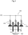
- Figure 1-3 schematically illustrates three different pixel-arrays of the optical sensor, consisting of a plurality of sensing elements designed according to well-known layouts.
- the schematic depicted in Fig.1 shows a pixel-array 100 of an optical sensor realized in CMOS technology comprising a plurality of sensing elements 110 (e.g. SPAD), arranged in a two-dimensional matrix, and having a first electrode (110a) connected to a potential V1 and a second electrode (110b) connected to a common potential node V2 (115).
- sensing elements 110 e.g. SPAD
- each sensing element is configured to include a photodiode active area (110c), which, in its simplest form, is realized in a p-n (or n-p) reversed biased junctions so that the n (or p) regions are depleted from charge carriers (such as electron/hole pairs) and, thence, incident photons generate electron/hole pairs collected by the depletion regions of the photodiode.
- the p-n junction is reversed biased to above the breakdown voltage so that, before to be collected, the electron (and the hole) acquires enough energy to create other pairs and initiate an avalanche process, thus amplifying the signal generated by an incident single photon.
- a quenching resistor, 120 is used to stop the avalanche process.
- each incoming photon may be detected, resulting in a strong current pulse of few nanosecond duration.
- V1 is applied consecutively to each first electrode, while the potential V2 (e.g. ground potential) is applied simultaneously to all second electrodes.
- V2 e.g. ground potential
- the standard method employs a trench isolation structure (solid bar 230 in Fig.2 ), filled with conductive material (e.g. metal) or other opaque material.
- conductive material e.g. metal
- the formation of the trench isolation structure provides for an optical isolation structure, but at the same time, it electrically isolates the sensing elements from each other, making impossible to connect all sensing elements to a common potential, V2.
- Fig.3 the standard method used to overcome the problem is shown.
- an additional contact 310 is added to each sensing element, in a way to apply the potential V2 (e.g. ground potential) to each second electrode of each sensing element consecutively.
- V2 e.g. ground potential
- the addition of a contact 310 to each sensing element requires the use of more silicon space of the pixel-array layout, thus decreasing the Fill Factor and thus the PDE.
- the proposed solution provides for a method of manufacturing of a BSI optical sensor according to a first and a second embodiments.
- Figure 4 shows an example of optical sensor obtained according to a first preferred embodiment of the proposed method.
- Fig.4 is a cross-sectional view of a BSI optical sensor 400, in a particular step of the manufacturing process, including:
- the BSI optical sensor 400 is manufactured according to the manufacturing process steps illustrated in the flow chart A of Fig.5 .
- the manufacturing process comprises the following manufacturing steps: 501) performing a standard CMOS frontside manufacturing process comprising the steps of forming a FS isolation structure (for example a shallow trench isolation structure (STI)), a plurality of interconnection layers and a plurality of contacts/via structures arranged in a multilevel isolation structure; 502) attaching a carrier wafer to the frontside surface of said multilevel isolation structure; 503) partially thinning the semiconductor substrate from the backside surface; 504) forming BSI deep trench isolation (DTI) structure from backside by Photo/Etch process steps landing at the bottom side of the FS isolation structure, having the form of a grid, surrounding each sensing element region; 505) depositing a first isolation layer covering the trench side and bottom walls of the DTI structure and a second conductive material, like W, Ti/W or Aluminum, filling the internal of the a FS isolation structure (for example a shallow trench isolation structure
- CMP Chemical Mechanical Polishing
- the BSI deep trench isolation (DTI) structure is manufactured in the form of staggered lines of trench, so as to ensuring optical isolation between the adjacent sensing elements of the pixel-array while maintaining the electrical continuity between said sensing elements.
- Figure 6 shows an example of a BSI optical sensor obtained according to a second embodiment of the proposed method.
- the top part of Fig.6 represents a top-down view of the BSI optical sensor 600 and the bottom part represents a cross-sectional view of the BSI optical sensor 600 cut along the direction BB', displayed in the top part of Fig.6 .
- the optical sensor obtained according to this second embodiment includes:
- the BSI optical sensor 600 is manufactured according to the manufacturing process steps illustrated by the flow chart B in Fig.7 .
- the manufacturing process comprises the following manufacturing steps: 701) performing a standard frontside manufacturing process comprising the steps of forming a FS isolation structure (for example a shallow trench isolation structure (STI)), a plurality of interconnection layers and a plurality of contacts/via structures arranged in a multilevel isolation structure; 702) attaching a carrier wafer to the frontside surface of said multilevel isolation structure; 703) partially remove the silicon substrate from the backside silicon surface; 704) forming BSI deep trench isolation (DTI) structure from backside by Photo/Etch process steps landing at the bottom side of the FS isolation structure, having the form of staggered lines of trench, separated by gaps, and surrounding each sensing element region; 705) depositing a first isolation layer covering the trench side and bottom walls of the DTI structure and a second conductive material, like Ti/W or Aluminum filling the internal of the BS
- a FS isolation structure for example a
- the proposed solution consists in configuring the backside deep trench isolation structure in form of staggered lines of trench, running parallel to each other and surrounding adjacent sensing elements, said staggered lines of trench consisting of trench portions separated by gaps filled with silicon substrate, so as to insure electrical continuity between the sensing elements of the pixel-array (e.g. SPAD array) through these silicon gaps, and in the same time creating an optical barrier to the cross talk.
- the exposed silicon substrate in the photodiode region acts as second electrode for the sensing element and a common potential can be applied to each second electrode ( Fig. 7 ).
Description
- The present invention relates generally to a method for manufacturing a backside illumination (BSI) optical sensor and more specifically to a method for manufacturing a BSI optical sensor having improved detection parameters, like reduced cross talk and enhanced photon detection efficiency (PDE). In particular, the invention provides a method for the isolation of the sensing elements of the BSI optical sensor compatible with the possibility of applying a common voltage bias to the sensing elements.
- The optical sensors have reached such a level of miniaturization and detection accuracy to be used in many fields.
- For example, optical sensors are currently used in automated driving system like ADAS (Advanced Driver Assistance System) to provide for distance measurement. Among this type of optical sensor there is the so-called Time of Flight (TOF) device, which is designed to detect the distance of a target object by measuring the time it takes for an electromagnetic wave (e.g. laser pulse) to return from a target object. The TOF device employs a very high sensitivity sensing element, as it is the Single Photon Avalanche Diodes (SPAD). The main components of a SPAD are: an avalanche photodiode operated above the breakdown voltage (Geiger mode), a quenching resistor, a first electrode (cathode) and a second electrode (anode). An electron-hole pair generated by incoming photon in the photodiode region (e.g. reversed biased p-n junction), which is biased above the breakdown voltage (multiplication region) can trigger an avalanche, due to the multiplication process by impact ionization of the space charge area of the photodiode. In this way a macroscopic electrical current is produced in response to the incident photon flow.
- The use of SPAD is not limited to the automotive market, but it is extensively employed in other market, such as the medical one. SPAD arrays (often referred to as Silicon Photo Multiplier or SiPM), has been adopted to replace photomultiplier tube (PMT) technology in photon counting applications, like Positron Emission Tomography (PET) technique, to observe metabolic processes in the body. The implementation of the SPAD technique in CMOS technology has further enhanced the advantage of SiPM technique, providing high dynamic range photon counting in picosecond timing.
- Referring again to the automotive market, the LIDAR (Light detection and ranging) technique, for example, employs the Near Infrared (NIR) light detection to measure the time of flight of an emitted laser pulse. In order to be sensitive to the NIR wavelength range, a SPAD-array optical sensor must have a Photo Detection Efficiency (PDE) greater than 10% in the range 850-910 nm of the electromagnetic spectrum. This is very difficult to be achieved with a conventional front side illuminated (FSI) CMOS optical sensor, due to the deep penetration distance of a NIR photon, which is absorbed deeply in the semiconductor substrate (e.g. Silicon substrate), with the consequence that the generated electron/hole pairs have poor chance to be collected in the avalanche photodiode region. Conversely, it can be achieved by a backside illuminated (BSI) CMOS optical sensor, which is configured to have all the sensing elements disposed near the backside surface, where the incoming photon are impinging from and, for this reason, most of the generated electron/hole pairs have more chances to be collected in the avalanche photodiode region.
- The major drawback that arises in SPAD array is the cross talk between neighboring sensing elements. The crosstalk may arise due to spurious avalanches in one sensing element that are caused by an avalanche in another sensing element, producing a spurious output current pulse also in absence of light (Dark Current). In order to limit the presence of photons travelling from one SPAD to the adjacent one, thus limiting the probability of triggering a secondary avalanche, (cross talk) and, consequently, the Dark Count Rate (DCR), the individual sensing element must be isolated from each other. Different isolation structures may be used. Generally, the isolation structures may be created in form of a trench etched from the frontside into the substrate adjacent to the sensing element region. Once the trench is formed it is usually filled with dielectric material. For example, according to
US patent 9,741,759 - Hence there is a desire to provide BSI optical sensor with improved characteristic parameters, such as a reduced cross talk and an improved Photo Detection Efficiency (PDE), without affect the Fill Factor.
- Document
US2012/025199 A1 shows a method of manufacturing a BSI CMOS image sensor according to the prior-art. - A general object of the present invention is, thence, to overcome the aforesaid technical problem that occurs when trying to reduce the cross talk by implementing an optical isolation structure, which isolates the sensing elements of an optical sensor from each other, thus inhibiting each sensitive element to be connected to a common voltage bias.
- Moreover, a specific object of the present invention is that of providing a method for manufacturing a backside illumination (BSI) CMOS optical sensor having improved detection parameters, said method comprising the step of creating an isolation structure between the adjacent sensing elements while keeping all sensing elements connected to a common voltage bias.
- These and other objects are achieved by the present invention in that it relates to the method of manufacturing an optical sensor, as defined in the appended claims.
According to a first embodiment of the present invention the method of manufacturing a backside illumination (BSI) CMOS optical sensor comprises the following steps: forming an isolation structure surrounding each sensing elements of the pixel-array in the form of trench grid structure, consisting of a first isolation structure (for example a Shallow Trench Isolation (STI) structure, or a LOCOS isolation structure, or an implantation area) created from the front side surface of the optical sensor and a deep trench isolation (DTI) structure etched from the backside surface of the optical sensor, after having thinned the silicon substrate from the backside, and landing in correspondence of the bottom surface of the frontside first isolation structure; filling the backside DTI structure with a first insulating material and a second opaque material (e.g. metal), suitable to reduce the cross talk; planarizing the backside surface of the optical sensor from the backside so as to expose the silicon surface in correspondence of each sensing element; depositing an additional low-resistivity layer on the backside surface, connecting the exposed silicon surface and providing a common voltage applying structure to all sensing elements of the pixel-array. Preferably, the additional low-resistivity layer consists of amorphous-silicon material, which has the advantage to filter the UV and Visible light, allowing only the NIR light to be detected. According to a second embodiment of the present invention, the method of manufacturing a backside illumination (BSI) CMOS optical sensor comprises the following steps: forming an isolation structure surrounding each sensing elements of the pixel-array in the form of staggered lines of trench, each line of trench consisting of trench portions separated by gaps, filled with silicon substrate, which are staggered with respect the trench portions belonging to a parallel line of trench; said isolation structure consisting of a first isolation structure (for example a Shallow Trench Isolation (STI) structure, or a LOCOS isolation structure, or an implantation area) created from the front side surface of the optical sensor and a second deep trench isolation (DTI) structure etched from the thinned backside surface of the optical sensor, and landing in correspondence of the bottom surface of the frontside first isolation structure; filling the backside DTI structure with opaque material, suitable to reduce the cross talk; planarizing the backside surface of the optical sensor so as to expose the silicon backside surface in correspondence of each sensing element and in correspondence of the silicon gaps, said exposed silicon backside surface providing a common voltage applying structure to all the sensing elements of the pixel-array. - For a better understanding of the present invention, preferred embodiments, which are intended purely by way of example and are not to be construed as limiting, will now be described with reference to the attached drawings (not to scale), where:
-
Figure 1 shows a schematic of the pixel-array of a known semiconductor optical sensor, where the sensing elements are connected in parallel to a common voltage bias; -
Figure 2 shows a schematic of the pixel-array of a known semiconductor optical sensor, where the sensing elements are separated by isolation structure (solid bars); -
Figure 3 shows a schematic of the pixel-array of a known semiconductor optical sensor, where the sensing elements are separated by an isolation structure (solid bars) and are connected to a common voltage bias through a single contact included in each sensing element; -
Figure 4 shows the cross section of a semiconductor BSI optical sensor, obtained with the claimed method, according to a first embodiment; -
Figure 5 shows the flow chart illustrating the method of manufacturing of the semiconductor BSI optical sensor according to a first embodiment; -
Figure 6 shows the top-down and the cross section of a semiconductor BSI optical sensor, obtained with the claimed method, according to a second embodiment; -
Figure 7 shows the flow chart illustrating the method of manufacturing of the semiconductor BSI optical sensor according to a second embodiment. - The following discussion is presented to enable a person skilled in the art to make and use the invention. Various modifications to the embodiments will be readily apparent to those skilled in the art, without departing from the scope of the present invention as claimed. Thus, the present invention is not intended to be limited to the embodiments shown and described, but is to be accorded the widest scope consistent with the principles and features disclosed herein and defined in the appended claims.
- As it will be discussed in detail in the following, an aspect of the present invention provides a method of manufacturing a BSI optical sensor, configured to have all the sensing elements (e.g. SPADs) of the pixel-array (e.g. SiPM) separated by an isolation structure in order to decrease the cross talk, said single elements being connected to a common voltage applying structure, provided from the backside of the optical sensor, in a way to not affect the Fill Factor.
-
Figure 1-3 schematically illustrates three different pixel-arrays of the optical sensor, consisting of a plurality of sensing elements designed according to well-known layouts. - For example, the schematic depicted in
Fig.1 shows a pixel-array 100 of an optical sensor realized in CMOS technology comprising a plurality of sensing elements 110 (e.g. SPAD), arranged in a two-dimensional matrix, and having a first electrode (110a) connected to a potential V1 and a second electrode (110b) connected to a common potential node V2 (115). In particular, each sensing element is configured to include a photodiode active area (110c), which, in its simplest form, is realized in a p-n (or n-p) reversed biased junctions so that the n (or p) regions are depleted from charge carriers (such as electron/hole pairs) and, thence, incident photons generate electron/hole pairs collected by the depletion regions of the photodiode. The p-n junction is reversed biased to above the breakdown voltage so that, before to be collected, the electron (and the hole) acquires enough energy to create other pairs and initiate an avalanche process, thus amplifying the signal generated by an incident single photon. A quenching resistor, 120, is used to stop the avalanche process. In this way each incoming photon may be detected, resulting in a strong current pulse of few nanosecond duration. In the standard approach the potential V1 is applied consecutively to each first electrode, while the potential V2 (e.g. ground potential) is applied simultaneously to all second electrodes. Hence, all the sensing elements of the pixel-array are connected in parallel to a common voltage bias, V1-V2. - To isolate the SPADs from each other with the aim of reducing the cross talk, the standard method employs a trench isolation structure (
solid bar 230 inFig.2 ), filled with conductive material (e.g. metal) or other opaque material. As depicted inFig.2 , the formation of the trench isolation structure provides for an optical isolation structure, but at the same time, it electrically isolates the sensing elements from each other, making impossible to connect all sensing elements to a common potential, V2. - In
Fig.3 the standard method used to overcome the problem is shown. By this method anadditional contact 310 is added to each sensing element, in a way to apply the potential V2 (e.g. ground potential) to each second electrode of each sensing element consecutively. The addition of acontact 310 to each sensing element requires the use of more silicon space of the pixel-array layout, thus decreasing the Fill Factor and thus the PDE. - To overcome the aforementioned problem, the proposed solution provides for a method of manufacturing of a BSI optical sensor according to a first and a second embodiments.
- For a better understanding of the present invention,
Figure 4 shows an example of optical sensor obtained according to a first preferred embodiment of the proposed method. In particular,Fig.4 is a cross-sectional view of a BSIoptical sensor 400, in a particular step of the manufacturing process, including: - a
frontside FS surface 410 and abackside BS surface 411; - a semiconductor substrate (e.g. silicon substrate) 401 having a
first surface 401a and asecond surface 401b facing each other; - at least a
first sensing element 402a and asecond sensing element 402b formed in saidsemiconductor substrate 401 and separated by a frontside isolation structure (for example a shallow trench isolation (STI) structure) 403; - a frontside voltage applying device 404 electrically connected to said at least first or second sensing elements from the
FS surface 401a of said semiconductor substrate; - an insulating
layer 406, formed as a multilayer, comprising at least afirst interconnection level 407 and ametal contact 408; - a
carrier semiconductor substrate 409 attached to thefrontside surface 410 of said optical sensor; - a backside deep trench isolation (DTI)
structure 405, surrounding the at least one and second sensing elements, etched from saidBS surface 401b and landing to the bottom side of theFS isolation structure 403, said BS DTI structure being filled with a first insulatingmaterial 405a (e.g. Silicon Oxide) covering the side walls and the bottom of the trench and with a secondconductive material 405b (e.g. Tungsten) filling the inside of said BS DTI structure; - an additional low-resistivity layer 412 (e.g. amorphous-silicon layer) deposited on the
BS surface 401b and connecting the at least first andsecond sensing elements - According to a first preferred embodiment of the present invention the BSI
optical sensor 400 is manufactured according to the manufacturing process steps illustrated in the flow chart A ofFig.5 . According to this preferred embodiment, the manufacturing process comprises the following manufacturing steps: 501) performing a standard CMOS frontside manufacturing process comprising the steps of forming a FS isolation structure (for example a shallow trench isolation structure (STI)), a plurality of interconnection layers and a plurality of contacts/via structures arranged in a multilevel isolation structure; 502) attaching a carrier wafer to the frontside surface of said multilevel isolation structure; 503) partially thinning the semiconductor substrate from the backside surface; 504) forming BSI deep trench isolation (DTI) structure from backside by Photo/Etch process steps landing at the bottom side of the FS isolation structure, having the form of a grid, surrounding each sensing element region; 505) depositing a first isolation layer covering the trench side and bottom walls of the DTI structure and a second conductive material, like W, Ti/W or Aluminum, filling the internal of the BSI DTI structure; 506) planarizing the backside surface (e.g. by Chemical Mechanical Polishing, CMP) to remove all the conductive material in excess on the backside surface and forming a low resistivity layer by depositing an amorphous-silicon layer, doping said amorphous-silicon layer (e.g. by implantation) and annealing it (e.g. by thermal laser anneal, LTA, or microwave anneal or other methodologies non impacting the underneath layers) to convert the amorphous-silicon layer in a low resistivity layer. Eventually a proper ARC layer can be applied on top of the low resistivity layer to improve the transmission of near infra-red (NIR) radiation. - The advantages of the present invention are clear from the foregoing. In particular, it is important to underline the fact that with the aforementioned method all the at least first and second sensing elements of the optical sensor pixel-array (e.g. SPAD array) are connected to the same backside potential (e.g. ground potential) by contacting the low resistivity layer with only one or very few contacts placed in the front side of the optical sensor (not shown in
Fig.4 ). It is also advantageous to use amorphous-silicon layer as additional low-resistivity material, because it contributes to filter UV/visible radiation in case of a near infra-red (NIR) light detection. - According to a second embodiment of the present invention the BSI deep trench isolation (DTI) structure is manufactured in the form of staggered lines of trench, so as to ensuring optical isolation between the adjacent sensing elements of the pixel-array while maintaining the electrical continuity between said sensing elements. For a better understanding,
Figure 6 shows an example of a BSI optical sensor obtained according to a second embodiment of the proposed method. In particular, the top part ofFig.6 represents a top-down view of the BSIoptical sensor 600 and the bottom part represents a cross-sectional view of the BSIoptical sensor 600 cut along the direction BB', displayed in the top part ofFig.6 . The optical sensor obtained according to this second embodiment includes: - a front side FS surface 610 and a
backside BS surface 611; - a
semiconductor substrate 601 having afirst surface 601a and asecond surface 601b facing each other; - at least a
first sensing element 602a and asecond sensing element 602b formed in said semiconductor substrate and separated by a FS isolation structure (for example a shallow trench isolation (STI) structure) 603; - a front side
voltage applying device 604 electrically connected to said at least first or second sensing elements from theFS surface 601a of said semiconductor substrate; - an insulating
layer 606, formed as a multilayer, comprising at least afirst interconnection layer 607 and ametal contact 608; - a
carrier semiconductor substrate 609 attached to thefrontside surface 610 of said optical sensor; - a backside BS deep trench isolation (DTI) structure, surrounding the at least one and second sensing element,
- According to a second embodiment of the present invention the BSI
optical sensor 600 is manufactured according to the manufacturing process steps illustrated by the flow chart B inFig.7 . According to this method, the manufacturing process comprises the following manufacturing steps: 701) performing a standard frontside manufacturing process comprising the steps of forming a FS isolation structure (for example a shallow trench isolation structure (STI)), a plurality of interconnection layers and a plurality of contacts/via structures arranged in a multilevel isolation structure; 702) attaching a carrier wafer to the frontside surface of said multilevel isolation structure; 703) partially remove the silicon substrate from the backside silicon surface; 704) forming BSI deep trench isolation (DTI) structure from backside by Photo/Etch process steps landing at the bottom side of the FS isolation structure, having the form of staggered lines of trench, separated by gaps, and surrounding each sensing element region; 705) depositing a first isolation layer covering the trench side and bottom walls of the DTI structure and a second conductive material, like Ti/W or Aluminum filling the internal of the BSI DTI structure; 706) planarizing the backside surface (e.g. by Chemical Mechanical Polishing, CMP) to remove all the conductive layer in excess on the backside surface. - The advantages of the present invention are clear from the foregoing. In particular, it is important to underline that the proposed solution consists in configuring the backside deep trench isolation structure in form of staggered lines of trench, running parallel to each other and surrounding adjacent sensing elements, said staggered lines of trench consisting of trench portions separated by gaps filled with silicon substrate, so as to insure electrical continuity between the sensing elements of the pixel-array (e.g. SPAD array) through these silicon gaps, and in the same time creating an optical barrier to the cross talk. According the aforementioned method the exposed silicon substrate in the photodiode region acts as second electrode for the sensing element and a common potential can be applied to each second electrode (
Fig. 7 ). - Finally, it is clear that numerous modifications and variants can be made to the present invention, all falling within the scope of the invention, as defined in the appended claims.
Claims (14)
- A method of manufacturing a backside illumination (BSI) CMOS optical sensor having improved cross talk and enhanced photon detection efficiency (PDE), said method comprising the following operations:providing a semiconductor wafer having a semiconductor substrate (401), a first surface (401a) and a second surface (401b), facing each other;performing a standard CMOS frontside manufacturing process comprising the steps of forming at least a first sensing element (402a) and a second sensing elements (402b) in the substrate between said first and second semiconductor surface,forming at least one insulating layer (406) on said semiconductor substrate first surface, at least a first interconnection layer (407) and at least one metal contact (408), said at least first interconnection layer and said at least one metal contact being embedded in the at least one insulating layer;providing a carrier semiconductor substrate (409) and attaching said carrier semiconductor substrate to said at least one insulating layer;thinning the semiconductor wafer by removing material from said semiconductor substrate second surface (401b);forming a backside deep trench isolation (DTI) structure (405) in the substrate surrounding said at least first and second sensing elements, said DTI structure extending from the thinned second surface;filling said DTI structure with first insulating material (405a) covering the side walls and the bottom of the trench and with a second conductive material (405b) filling the inside of said deep trench isolation (DTI) structure;planarizing the semiconductor wafer from said thinned second surface, so as to expose said semiconductor substrate (401) in the region of the at least first and second sensing elements, said at least first and second sensing elements being surrounded by said DTI structure;forming a common voltage applying structure from said thinned second surface contacting said deep trench isolation (DTI) structure and said semiconductor substrate in the at least first and second sensing elements.
- The method of claim 1, wherein said deep trench isolation (DTI) structure (405) has the form of a trench grid structure surrounding said at least first and second sensing element.
- The method of claim 2, wherein the step of forming a common voltage applying structure from said thinned second surface contacting all said first and second sensing element comprises the step of forming a low resistivity layer (412) on the thinned second surface connecting said trench grid structure and said semiconductor substrate in the at least first and second sensing elements.
- The method of claim 3, wherein the step of forming said low resistivity layer (412) on the thinned second surface comprises the following process steps:depositing an amorphous-silicon layer;doping said amorphous-silicon layer by implantation process;and annealing said amorphous-silicon layer by thermal laser anneal (LTA) or microwave anneal or other methodologies non impacting the underneath layers.
- The method of claim 1, wherein said deep trench isolation (DTI) structure (405) has the form of staggered lines of trench, each line of trenches consisting of trench portions separated by gaps filled with semiconductor substrate, said trench portions belonging to one line of trenches being staggered with respect to the trench portion belonging to the parallel line of trench.
- The method of claim 5, wherein said gaps between said trench portions are configured to provide a common voltage applying structure from said thinned second surface to said at least first and second sensing elements.
- The method of any of the preceding claims, wherein said first insulating material (405a) is Silicon Oxide.
- The method of any of the preceding claims, wherein said second conductive material (405b) is an opaque material.
- The method of claim 8, wherein said opaque material (405b) is made of metal.
- The method of claim 9, wherein said metal is chosen in a set composed of: Titanium, Titanium Nitride, Tungsten, Aluminum.
- The method of claim 1, wherein said standard CMOS frontside manufacturing process further comprises the step of forming a first isolation structure in the semiconductor substrate surrounding said at least first and second sensing elements, said first isolation structure extending from said semiconductor first surface.
- The method of claim 11, wherein said first isolation structure formed in the semiconductor substrate surrounding said at least first and second sensing elements is a Shallow Trench Isolation (STI) structure.
- The method of claim 11, wherein said first isolation structure formed in the semiconductor substrate surrounding said at least first and second sensing elements is a LOCOS structure.
- The method of claim 11, wherein said first isolation structure formed in the semiconductor substrate surrounding said at least first and second sensing elements is an implanted region.
Applications Claiming Priority (2)
| Application Number | Priority Date | Filing Date | Title |
|---|---|---|---|
| IT201900016523 | 2019-09-18 | ||
| PCT/EP2020/075657 WO2021052912A1 (en) | 2019-09-18 | 2020-09-14 | Method for manufacturing a backside illumination optical sensor with improved detection parameters |
Publications (3)
| Publication Number | Publication Date |
|---|---|
| EP4032124A1 EP4032124A1 (en) | 2022-07-27 |
| EP4032124B1 true EP4032124B1 (en) | 2023-11-01 |
| EP4032124C0 EP4032124C0 (en) | 2023-11-01 |
Family
ID=69191163
Family Applications (1)
| Application Number | Title | Priority Date | Filing Date |
|---|---|---|---|
| EP20771852.9A Active EP4032124B1 (en) | 2019-09-18 | 2020-09-14 | Method for manufacturing a backside illumination optical sensor with improved detection parameters |
Country Status (6)
| Country | Link |
|---|---|
| US (1) | US20220344387A1 (en) |
| EP (1) | EP4032124B1 (en) |
| JP (1) | JP2022549602A (en) |
| KR (1) | KR20220062014A (en) |
| CN (1) | CN114402436A (en) |
| WO (1) | WO2021052912A1 (en) |
Family Cites Families (3)
| Publication number | Priority date | Publication date | Assignee | Title |
|---|---|---|---|---|
| US8390089B2 (en) * | 2010-07-27 | 2013-03-05 | Taiwan Semiconductor Manufacturing Company, Ltd. | Image sensor with deep trench isolation structure |
| KR102180102B1 (en) * | 2014-03-07 | 2020-11-17 | 삼성전자주식회사 | Image Sensor and Method of Fabricating the Same |
| CN109716525B (en) * | 2016-09-23 | 2020-06-09 | 苹果公司 | Stacked back side illumination SPAD array |
-
2020
- 2020-09-14 KR KR1020227011050A patent/KR20220062014A/en unknown
- 2020-09-14 WO PCT/EP2020/075657 patent/WO2021052912A1/en active Search and Examination
- 2020-09-14 US US17/642,511 patent/US20220344387A1/en active Pending
- 2020-09-14 JP JP2022517453A patent/JP2022549602A/en active Pending
- 2020-09-14 EP EP20771852.9A patent/EP4032124B1/en active Active
- 2020-09-14 CN CN202080065330.2A patent/CN114402436A/en active Pending
Also Published As
| Publication number | Publication date |
|---|---|
| JP2022549602A (en) | 2022-11-28 |
| WO2021052912A1 (en) | 2021-03-25 |
| KR20220062014A (en) | 2022-05-13 |
| EP4032124A1 (en) | 2022-07-27 |
| US20220344387A1 (en) | 2022-10-27 |
| CN114402436A (en) | 2022-04-26 |
| EP4032124C0 (en) | 2023-11-01 |
Similar Documents
| Publication | Publication Date | Title |
|---|---|---|
| US11329185B2 (en) | Avalanche diode along with vertical PN junction and method for manufacturing the same field | |
| US9257589B2 (en) | Single photon avalanche diode with second semiconductor layer burried in epitaxial layer | |
| US9773930B2 (en) | Integrated circuit with reflective material in trenches and related methods | |
| US10353057B2 (en) | Photodetector and LIDAR system including the photodetector | |
| EP2592661B1 (en) | Lateral avalanche photodiode device and method of production | |
| US8723100B2 (en) | Method of detecting impinging position of photons on a geiger-mode avalanche photodiode, related geiger-mode avalanche photodiode and fabrication process | |
| US7667400B1 (en) | Back-illuminated Si photomultipliers: structure and fabrication methods | |
| US9231006B2 (en) | Semiconductor element and solid-state imaging device | |
| US11830960B2 (en) | Avalanche photodiode sensor and sensor device | |
| US9978802B2 (en) | Multiband optoelectronic device for colorimetric applications and related manufacturing process | |
| US20110298079A1 (en) | Semiconductor element and solid-state imaging device | |
| KR101127982B1 (en) | A silicon photomultiplier with backward light-receivig structure, the manufacturing method thereof and the radiation detector using the same | |
| Liu et al. | A wide spectral response single photon avalanche diode for backside-illumination in 55-nm CMOS process | |
| EP4032124B1 (en) | Method for manufacturing a backside illumination optical sensor with improved detection parameters | |
| US20230131505A1 (en) | Photodetectors with a deep trench isolation region that includes a bragg mirror | |
| CN115332384A (en) | Single photon detector and manufacturing method thereof | |
| US20230026004A1 (en) | Ranging image sensor and method for manufacturing same | |
| EP2793273B1 (en) | Silicon photomultiplier with very low optical cross-talk and improved readout | |
| US20230062980A1 (en) | Opto-electronic device for detecting and localizing objects for lidar applications | |
| WO2011071483A1 (en) | Back-illuminated si photomultipliers: structure and fabrication methods | |
| CN117855316A (en) | Photodetector and method of forming the same | |
| CN117855317A (en) | Photodetector and method of forming the same | |
| CN114551631A (en) | Back-illuminated silicon-based single photon avalanche diode structure and photoelectric detector |
Legal Events
| Date | Code | Title | Description |
|---|---|---|---|
| STAA | Information on the status of an ep patent application or granted ep patent |
Free format text: STATUS: UNKNOWN |
|
| STAA | Information on the status of an ep patent application or granted ep patent |
Free format text: STATUS: THE INTERNATIONAL PUBLICATION HAS BEEN MADE |
|
| PUAI | Public reference made under article 153(3) epc to a published international application that has entered the european phase |
Free format text: ORIGINAL CODE: 0009012 |
|
| STAA | Information on the status of an ep patent application or granted ep patent |
Free format text: STATUS: REQUEST FOR EXAMINATION WAS MADE |
|
| 17P | Request for examination filed |
Effective date: 20220317 |
|
| AK | Designated contracting states |
Kind code of ref document: A1 Designated state(s): AL AT BE BG CH CY CZ DE DK EE ES FI FR GB GR HR HU IE IS IT LI LT LU LV MC MK MT NL NO PL PT RO RS SE SI SK SM TR |
|
| DAV | Request for validation of the european patent (deleted) | ||
| DAX | Request for extension of the european patent (deleted) | ||
| GRAP | Despatch of communication of intention to grant a patent |
Free format text: ORIGINAL CODE: EPIDOSNIGR1 |
|
| STAA | Information on the status of an ep patent application or granted ep patent |
Free format text: STATUS: GRANT OF PATENT IS INTENDED |
|
| INTG | Intention to grant announced |
Effective date: 20230614 |
|
| GRAS | Grant fee paid |
Free format text: ORIGINAL CODE: EPIDOSNIGR3 |
|
| GRAA | (expected) grant |
Free format text: ORIGINAL CODE: 0009210 |
|
| STAA | Information on the status of an ep patent application or granted ep patent |
Free format text: STATUS: THE PATENT HAS BEEN GRANTED |
|
| AK | Designated contracting states |
Kind code of ref document: B1 Designated state(s): AL AT BE BG CH CY CZ DE DK EE ES FI FR GB GR HR HU IE IS IT LI LT LU LV MC MK MT NL NO PL PT RO RS SE SI SK SM TR |
|
| REG | Reference to a national code |
Ref country code: GB Ref legal event code: FG4D |
|
| REG | Reference to a national code |
Ref country code: CH Ref legal event code: EP |
|
| REG | Reference to a national code |
Ref country code: IE Ref legal event code: FG4D |
|
| REG | Reference to a national code |
Ref country code: DE Ref legal event code: R096 Ref document number: 602020020327 Country of ref document: DE |
|
| U01 | Request for unitary effect filed |
Effective date: 20231122 |
|
| U07 | Unitary effect registered |
Designated state(s): AT BE BG DE DK EE FI FR IT LT LU LV MT NL PT SE SI Effective date: 20231128 |
|
| PG25 | Lapsed in a contracting state [announced via postgrant information from national office to epo] |
Ref country code: GR Free format text: LAPSE BECAUSE OF FAILURE TO SUBMIT A TRANSLATION OF THE DESCRIPTION OR TO PAY THE FEE WITHIN THE PRESCRIBED TIME-LIMIT Effective date: 20240202 |
|
| PG25 | Lapsed in a contracting state [announced via postgrant information from national office to epo] |
Ref country code: IS Free format text: LAPSE BECAUSE OF FAILURE TO SUBMIT A TRANSLATION OF THE DESCRIPTION OR TO PAY THE FEE WITHIN THE PRESCRIBED TIME-LIMIT Effective date: 20240301 |