EP4031803B1 - Leuchtdiodenfilamentanordnung mit mindestens einer biegeeinheit - Google Patents
Leuchtdiodenfilamentanordnung mit mindestens einer biegeeinheit Download PDFInfo
- Publication number
- EP4031803B1 EP4031803B1 EP20771871.9A EP20771871A EP4031803B1 EP 4031803 B1 EP4031803 B1 EP 4031803B1 EP 20771871 A EP20771871 A EP 20771871A EP 4031803 B1 EP4031803 B1 EP 4031803B1
- Authority
- EP
- European Patent Office
- Prior art keywords
- led filament
- bending unit
- channel
- led
- arrangement
- Prior art date
- Legal status (The legal status is an assumption and is not a legal conclusion. Google has not performed a legal analysis and makes no representation as to the accuracy of the status listed.)
- Active
Links
Images


Classifications
-
- F—MECHANICAL ENGINEERING; LIGHTING; HEATING; WEAPONS; BLASTING
- F21—LIGHTING
- F21K—NON-ELECTRIC LIGHT SOURCES USING LUMINESCENCE; LIGHT SOURCES USING ELECTROCHEMILUMINESCENCE; LIGHT SOURCES USING CHARGES OF COMBUSTIBLE MATERIAL; LIGHT SOURCES USING SEMICONDUCTOR DEVICES AS LIGHT-GENERATING ELEMENTS; LIGHT SOURCES NOT OTHERWISE PROVIDED FOR
- F21K9/00—Light sources using semiconductor devices as light-generating elements, e.g. using light-emitting diodes [LED] or lasers
- F21K9/20—Light sources comprising attachment means
- F21K9/23—Retrofit light sources for lighting devices with a single fitting for each light source, e.g. for substitution of incandescent lamps with bayonet or threaded fittings
- F21K9/232—Retrofit light sources for lighting devices with a single fitting for each light source, e.g. for substitution of incandescent lamps with bayonet or threaded fittings specially adapted for generating an essentially omnidirectional light distribution, e.g. with a glass bulb
-
- F—MECHANICAL ENGINEERING; LIGHTING; HEATING; WEAPONS; BLASTING
- F21—LIGHTING
- F21K—NON-ELECTRIC LIGHT SOURCES USING LUMINESCENCE; LIGHT SOURCES USING ELECTROCHEMILUMINESCENCE; LIGHT SOURCES USING CHARGES OF COMBUSTIBLE MATERIAL; LIGHT SOURCES USING SEMICONDUCTOR DEVICES AS LIGHT-GENERATING ELEMENTS; LIGHT SOURCES NOT OTHERWISE PROVIDED FOR
- F21K9/00—Light sources using semiconductor devices as light-generating elements, e.g. using light-emitting diodes [LED] or lasers
- F21K9/20—Light sources comprising attachment means
- F21K9/23—Retrofit light sources for lighting devices with a single fitting for each light source, e.g. for substitution of incandescent lamps with bayonet or threaded fittings
- F21K9/235—Details of bases or caps, i.e. the parts that connect the light source to a fitting; Arrangement of components within bases or caps
-
- F—MECHANICAL ENGINEERING; LIGHTING; HEATING; WEAPONS; BLASTING
- F21—LIGHTING
- F21Y—INDEXING SCHEME ASSOCIATED WITH SUBCLASSES F21K, F21L, F21S and F21V, RELATING TO THE FORM OR THE KIND OF THE LIGHT SOURCES OR OF THE COLOUR OF THE LIGHT EMITTED
- F21Y2107/00—Light sources with three-dimensionally disposed light-generating elements
- F21Y2107/70—Light sources with three-dimensionally disposed light-generating elements on flexible or deformable supports or substrates, e.g. for changing the light source into a desired form
-
- F—MECHANICAL ENGINEERING; LIGHTING; HEATING; WEAPONS; BLASTING
- F21—LIGHTING
- F21Y—INDEXING SCHEME ASSOCIATED WITH SUBCLASSES F21K, F21L, F21S and F21V, RELATING TO THE FORM OR THE KIND OF THE LIGHT SOURCES OR OF THE COLOUR OF THE LIGHT EMITTED
- F21Y2115/00—Light-generating elements of semiconductor light sources
- F21Y2115/10—Light-emitting diodes [LED]
Definitions
- the present disclosure relates generally to the field of solid state lighting. Specifically, it relates to light emitting diode (LED) filament arrangements comprising bending units for inducing bends in a LED filament.
- LED light emitting diode
- Incandescent lamps are rapidly being replaced by light emitting diode (LED) based lighting solutions.
- the look and aesthetic provided by incandescent bulbs is nevertheless still appreciated by consumers who also value the opportunity of using retrofit LED lamps in existing luminaires.
- a goal for developers of LED-based lighting is thus to provide decorative retrofit LED lamps providing an aesthetically pleasing appearance and illumination.
- LED filaments In order to provide sufficient illumination from a LED lamp, several short LED filaments may be used. However, as each LED filament needs to be individually electrically connected, the production may be complicated.
- Another option is to use longer, flexible filaments which may be bent to produce various configurations. Such solutions, on the other hand, may present irregular behavior as LED filament portions which are bent or under stress may be susceptible for reliability issues.
- a light emitting diode, LED, filament arrangement comprises an elongated, flexible LED filament having a plurality of LEDs arranged along the elongation (i.e. along a direction of elongation) of the LED filament.
- the arrangement further comprises a bending unit having a body in which an at least partially curved channel is formed. A portion of the LED filament is arranged within the channel of the bending unit.
- the bending unit is adapted to induce a bend in the LED filament.
- the length of the bending unit is 0.05 to 0.3 times the length of the LED filament.
- LED filaments are not arranged within a bending unit.
- Providing a bending unit for inducing a bend in a LED filament may increase the reliability of the LED filament arrangement.
- a LED filament arrangement employing a bending unit for inducing a bend in a LED filament may better retain its initial (intended) shape.
- the bending unit may hold the LED filament in its bent form, such that it is not straightened or bent too much.
- electrical connections between LEDs may for example be damaged.
- many LED filaments comprise a substrate, on which the LEDs are arranged, and an encapsulant covering the LEDs and at least a side of the substrate.
- the bending unit may be pre-formed to induce a desired bend/orientation to the flexible LED filament. As such, a desired decorative appearance may be obtained. Further, the light distribution may be enhanced, as a more optimal arrangement and orientation of the LED filament may be obtained and maintained.
- the bending unit may have a length in the range 5-50 mm. Specifically, the bending unit may have a length in the range 8-30 mm. More specifically, the bending unit may have a length in the range 10-20 mm.
- the length of the bending unit is defined relative to the length of the LED filament.
- the length of the bending unit is 0.05 to 0.3 times the length of the LED filament.
- the length of the bending unit may be 0.08 to 0.25 times the length of the LED filament. More specifically, the length of the bending unit may be in the range 0.1 to 0.2 times the length of the LED filament.
- the bending unit may further have an inner diameter, i.e. a diameter of the channel.
- the bending unit may have an inner diameter (i.e. a diameter of the channel) in the range 1-10 mm.
- the bending unit may have an inner diameter in the range 2-7 mm. More specifically, the bending units may have an inner diameter in the range 3-5 mm.
- the inner diameter of the bending unit may be defined relative to the diameter of the LED filament.
- the inner diameter of the bending unit may be 0.8 to 1.5 times the diameter of the LED filament.
- the inner diameter of the bending unit may be 0.9 to 1.3 times the diameter of the LED filament.
- the inner diameter of the bending unit may be 1 to 1.2 times the diameter of the LED filament.
- the bending unit may be at least partially light-transmissive.
- the body of the bending unit may be translucent or transparent.
- Such embodiments may provide improved light distribution (or increased illumination) as light emitted by the portion of the LED filament which is arranged within the channel is not blocked.
- Such at least partially light-transmissive bending units may comprise a material such as glass or a polymer.
- the bending unit may be at least partially light-blocking.
- Arrangements comprising such bending units may give the illusion or appearance of multiple, shorter LED filaments being employed.
- At least partially light-blocking bending units may comprise a material such as copper or aluminum.
- the bending unit may comprise a material with a thermal conductivity which is higher than, or equal to, 200 Wm -1 K -1 .
- Such embodiments may provide improved thermal management. For instance, transfer of heat generated by the portion of the LED filament arranged within the channel may be improved such that the LED filament remains at an adequate temperature.
- the body may comprise a material having a thermal conductivity of at least 250 Wm -1 K -1 . More specifically, the body may comprise a material having a thermal conductivity of at least 350 Wm -1 K -1 .
- the body may comprise a high thermal conductive material such as aluminum, iron, steel or copper.
- the bending unit may comprise a slit, extending through the body along an elongation of the channel.
- the slit may be adapted for insertion of the LED filament into the channel.
- the slit may extend along the entire channel.
- the slit may further act as an opening for insertion of the LED filament into the channel.
- Such a slit may allow for the LED filament to be inserted sideways into the channel.
- the entire LED filament up until the desired portion may not need to be fed through the channel.
- the LED filament may not be unnecessarily bent.
- the width of the slit may be larger than the diameter of the LED filament, but smaller than the inner diameter or width of the channel.
- the width of the slit may be slightly smaller than the diameter of the LED filament.
- the LED filament may be inserted into the channel if the LED filament has a certain flexibility (for example, comprising a flexible encapsulant). The LED filament may thus be fixed in bending unit.
- the body of the bending unit may comprise a surface which defines a wall of the channel.
- the shape of the wall may be adapted to the circumference of a type of LED filament, such that LED filaments of the type may fit in the channel.
- the surface defining a wall of the channel may comprise at least one recess.
- the surface of the wall may comprise at least two recesses.
- the surface may comprise at least three recesses.
- Such embodiments may provide improved thermal management.
- the recess may allow an air flow within the bending unit, which may carry off heat from the LED filament.
- the at least one recess may extend along an elongation of the channel.
- the at least one recess may extend along the entire length of the channel. Such embodiments may provide further improved thermal management.
- the surface of the body defining a wall of the channel may have a reflectivity of at least 85%.
- the surface/wall may have a reflectivity of at least 90%. More specifically, the surface/wall may have a reflectivity of at least 92%.
- a high reflectivity may allow for light to be reflected and be emitted at the ends of the bending unit. Less heat may be generated if the light is reflected instead of being absorbed by the bending units.
- the surface defining a wall of the channel may be coated with a coating layer comprising a metal.
- the coating layer may comprise silver or aluminum.
- a metal coating may improve the reflectivity of the surface.
- a metal coating may also improve the thermal conductivity of the surface.
- the metal layer may be applied using a deposition technique, such as for example physical vapor deposition or chemical vapor deposition.
- the surface defining a wall of the channel may be coated with a coating layer comprising a polymer and light-scattering particles.
- the polymer may be silicone.
- Light-scattering particles may e.g. comprise barium sulfate (BaSO 4 ), aluminum(III) oxide (Al 2 O 3 ), or titanium dioxide (TiO 2 ).
- a polymer coating with light-scattering particles may improve the light distribution of the bending unit.
- Such a coating layer may further increase the reflectivity of the surface.
- the coating layer may comprise a matrix material, such as a polymer matrix comprising particles.
- a matrix material such as a polymer matrix comprising particles.
- particles may comprise silver-based particles, aluminum-based particles, or light-scattering particles as described above.
- the portion of the LED filament which is arranged within the channel may comprise more than one LED.
- the portion of the LED filament which is arranged within the channel may comprise more than three LEDs.
- the portion of the LED filament which is arranged within the channel may comprise more than five LEDs.
- the portion of the LED filament which is arranged within the channel may comprise more than seven LEDs.
- the arrangement may comprise a plurality of bending units.
- Each bending unit may be adapted to induce a bend in the LED filament.
- the plurality of bending units may comprise at least three bending units. Specifically, the plurality of bending units may comprise at least five bending units. More specifically, the plurality of bending units may comprise at least seven bending units.
- each bending unit may be adapted to induce a bend in a separate portion of the LED filament.
- a plurality of bending units multiple bends may be induced in a single LED filament.
- a number of bends which would otherwise (i.e. without bending units) be impossible without reliability issues, may be induced in a single LED filament.
- the LED filament may, for example, be arranged in a crown shape, a zig-zag shape, or a spiral shape. It will be appreciated that many other shapes and arrangements may be possible with the use of bending units.
- the at least partial curvature of the channel may be rounded such that the channel has a U-shape.
- a rounded curvature of the channel may prevent sharp bends in the LED filament. As sharp bends may induce strain in some LED filaments, the reliability of the LED filament arrangement may be improved.
- the bending unit may form more than one bend.
- the bending unit may have a meander-shape.
- the bending unit may further have a spiral shape, forming one or more loops.
- the bending unit may have a tubular shape.
- the bending unit may have a rounded and hollow shape.
- a lighting device may be provided.
- the lighting device may comprise a LED filament arrangement as described above with reference to any of the preceding embodiments.
- the lighting device may further comprise an at least partially light-transmissive envelope which may at least partly envelop the LED filament arrangement.
- the lighting device may further comprise a base on which the envelope may be mounted. The base may be adapted to be connected to a luminaire socket.
- a lighting device may for example be a lamp or a bulb.
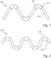
- the LED filament arrangement 100 comprises an elongated, flexible LED filament 110.
- the LED filament arrangement 100 further comprises three bending units 120.
- Each bending unit comprises a body, in which a channel 121 is defined or formed. Within the channel of each bending unit, a portion of the LED filament 110 is arranged.
- the channels 121 of the bending units 120 are curved, such that bends are induced in the LED filament 110.
- the bending units 120 are arranged such that the LED filament 110 forms a zig-zag shape (i.e. a shape having abrupt alternate left and right turns, or up and down turns or the like).
- portions of the LED filament 110 which are outside, and between, the bending units 120 are substantially straight.
- the bending units 120 are at least partially light-transmissive. Specifically, the bending units 120 are transparent, meaning that the portions of the LED filament 110 which are arranged within (inside) the channels 121 of the bending units 120 are visible through the bending units 120. As the bending units 120 are transparent, light emitted by the portions of the LED filament 110 which are arranged within the bending units 120 may be emitted through the bending units 120.
- the LED filament arrangement 200 illustrated in Fig 2 comprises a LED filament 210, which may be equivalent to the LED filament 110 as described with reference to Fig 1 .
- the LED filament arrangement 200 further comprises five bending units 220.
- the bending units each comprise a channel in which a portion of the LED filament 220 is arranged.
- these channels are not visible in Fig 2 .
- the curvature of the channels and the arrangement of the bending units induce an S-like curvature of the LED filament 210, with a bending unit 220 arranged at the outmost point of each turn of the S-curve.
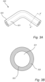
- a bending unit 320 in accordance with some embodiments, will be described.
- Fig 3a is an isometric view of the bending unit 320.
- Fig 3b is a cross-sectional view of the bending unit 320 taken along the line A-A', which is normal to the local extension of the channel.
- the bending unit 320 comprises a body 322, in which a channel 321 is formed.
- the body 322 is light-transmissive. It will be appreciated that, in other embodiments, the body may be at least partially light-blocking.
- the bending unit 320 (specifically the body 322) may comprise a material with a thermal conductivity of at least 200 Wm -1 K -1 .
- the bending unit 320 may comprise any high thermal conductive materials such as aluminum, iron, steel or copper.
- the bending unit 320 has a surface 323 which defines a wall of the channel 321.
- the surface 323 may be highly reflective, for example it may have a reflectivity of at least 85%.
- the surface 323 may have an even higher reflectivity, for example the reflectivity may be 90%, 92% or higher.
- the surface 323 may further comprise a coating layer.
- the coating layer may comprise a metal, such as silver or aluminum.
- the coating layer may also comprise a polymer, such as silicone, and light scattering particles, such as barium sulfate (BaSO 4 ), aluminum(III) oxide (Al 2 O 3 ), or titanium dioxide (TiO 2 ).
- the bending unit 320 of the present embodiment has a bent/curved tubular shape. As may be seen in Fig 3b , the cross section of the bending unit 320 has a substantially circular outer perimeter. Further, the surface 323 defining the wall of the channel is also substantially circular, in the cross-sectional view. It is appreciated that the channel and the body of the bending unit may have differently shaped cross sections in other embodiments. Specifically, the channel may be shaped to accommodate a type of LED filament with which it is intended to be used.
- Fig 4a is an isometric view of the LED filament arrangement 400.
- Fig 4b is a cross-sectional view taken along the line B-B' which is normal to the local extension of the bending unit 420 and the LED filament 410.
- the LED filament 410 may be equivalent to any of the LED filaments described with reference to the preceding figures.
- the bending unit 420 may be equivalent to any of the previously mentioned bending units described with reference to Figs 1-3 , except that it comprises a slit 424.
- the slit 424 provides an opening between the outside of the bending unit 420 and the channel, extending along the elongation of the bending unit 420.
- the slit 424 is adapted to allow for insertion of the LED filament 410 into the channel.
- the slit 424 is adapted to allow for sideways insertion of the LED filament 410 into the channel.
- the LED filament 410 may be aligned parallel with the slit 424. (Light) force may be applied to either the LED filament or the bending unit (or both) to press them together, and thus insert the LED filament 410 into the slit 424.
- the bending unit 420 may thus have a certain flexibility/elasticity, which may allow the bending unit 420 to be slightly deformed during the insertion, and then return back to its original shape.
- the LED filament may be thread into the channel of the bending unit by inserting one end of the LED filament into one end of the channel and threading it through the channel until the portion in which the bend is to be induced is within the channel.
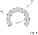
- Fig 5 is a cross-sectional view of a bending unit, similar to those shown in Figs 3b and 4b .
- the bending unit 520 may be equivalent to the bending unit 420 described with reference to Fig 4 , except that the surface 523 defining a wall of the channel comprises a plurality of recesses 525.
- the recesses 525 may extend along the entire length of the channel. Alternatively, the recesses 525 may only extend along some portions of the channel.
- bending units without a slit may comprise recesses as described herein with reference to Fig 5 .
- different embodiments may comprise fewer or more recesses along the inner surface 523 (i.e. the surface defining the wall of the channel).
- Fig 6a is an isometric view of the LED filament arrangement 600.
- Fig 6b is a cross-sectional view taken along the line C-C', similar to the cross-sectional views of Figs 3b , 4b and 5 .
- the LED filament arrangement 600 comprises a bending unit 620, which may be equivalent to bending units 120or 220 described above with reference to Figs 1 and 2 .
- the LED filament arrangement 600 further comprises a LED filament 610.
- the LED filament 610 comprises a flexible carrier 611 on which a plurality of LEDs 612 is arranged.
- the LEDs 612 are arranged in a single row on a first surface 613 of the carrier 611.
- the LEDs 612 are arranged along a direction of elongation (i.e. along the elongation) of the LED filament.
- An encapsulant 614 covers (encapsulates) the carrier 611 and the LEDs 612. Specifically, both the first surface 613 and a surface opposite to the first surface of the carrier 611 are covered by the encapsulant 614, giving the LED filament 610 a round shape (i.e. a round cross section as shown in Fig 6b ).
- the carrier 611 may be at least partially light-transmissive, such as translucent or transparent.
- the LEDs 612 are configured to emit light, which may be referred to as LED light. They may, for example, be configured to emit blue light (blue LEDs) or ultraviolet light (UV LEDs). Alternatively, red-green-blue (RGB) LEDs, which combine red, green and blue light to emit combined light, may be used.
- the encapsulant 614 may comprise a wavelength converting (luminescent) material. Such material may absorb light in a certain range of wavelengths and re-emit the light at a second, different, range of wavelengths, which may be referred to as converted light. The process of absorbing and re-emitting light at a different wavelength may be referred to as converting the wavelength of the light.
- Light emitted by a LED filament may be referred to as LED filament light.
- the LED filament light may comprise LED light and/or converted light.
- a portion of the LED filament 610 is arranged within the channel of the bending unit 620.
- the portion of the LED filament 610 which is covered by (i.e. arranged within) the bending unit 620 comprises four LEDs, in the present embodiment. This is however only an example and the bending unit may surround more or less than four LEDs.
- the LED filament may comprise fewer or more LEDs, which may be arranged in one or more rows, or in other configurations, on one or more sides of the carrier.
- a LED filament may provide LED filament light and comprise a plurality of light emitting diodes (LEDs) arranged in a linear array.
- the LED filament may have a length L and a width W, wherein L>5W.
- the LED filament may be arranged in a straight configuration or in a non-straight configuration such as for example a curved configuration, a 2D/3D spiral or a helix.
- the LEDs are arranged on an elongated carrier like for instance a substrate, that may be flexible (e.g. made of a polymer or metal e.g. a film or foil).
- the bending units described in the present disclosure may aid in arranging the LED filament in such configurations, by inducing bends in the LED filament.
- the LEDs may be arranged on at least one of these surfaces.
- the carrier may be reflective or light-transmissive, such as translucent and preferably transparent.
- the LED filament may comprise an encapsulant at least partly covering at least part of the plurality of LEDs.
- the encapsulant may also at least partly cover at least one of the first major or second major surface.
- the encapsulant may be a polymer material which may be flexible such as for example a silicone. Further, the LEDs may be arranged for emitting LED light e.g. of different colors or spectrums.
- the encapsulant may comprise a luminescent material that is configured to at least partly convert LED light into converted light.
- the luminescent material may be a phosphor such as an inorganic phosphor and/or quantum dots or rods.
- the LED filament may comprise multiple sub-filaments.
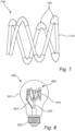
- the LED filament arrangement 700 comprises a LED filament 710 which may be equivalent to the LED filament 610 described with reference to Fig 6 .
- the LED filament arrangement 700 further comprises a plurality of bending units 720. More specifically the LED filament arrangement 700 comprises seven bending units 720.
- the bending units 720 may be equivalent to any bending units described above with reference to Figures 1-6 .
- the portions of the LED filament 710 which are not covered by (i.e. arranged within the channels of) the bending units 720 are of similar length, and with little or no curvature (i.e. substantially straight). Further, the bending units 720 are arranged with alternating orientation, such that the LED filament 710 forms a zig-zag shape. Moreover, the two end points of the LED filament 710 are arranged next to each other, such that the zig-zag shaped arrangement 700 forms a crown-like shape. Such arrangements, in which the bends have a sharper corner appearance, may be created with the use of bending units with improved reliability over similar arrangements without bending units.
- a lighting device 830 in accordance with some embodiments, will be described.
- the lighting device 830 comprises a LED filament arrangement 800.
- the LED filament arrangement 800 may be equivalent to the LED filament arrangement 700 described with reference to Fig 7 .
- LED filament arrangements of other shapes, such as shown in the other embodiments, may also be used.
- the lighting device 830 further comprises an at least partially light-transmissive envelope 831 which envelops the LED filament arrangement 800.
- the envelope 831 is transparent.
- the envelope 831 is mounted on a base 832.
- the base 832 is adapted to be connected with a socket of a luminaire.
- the illustrated embodiment is adapted to be connected with a socket of Edison type. However, other embodiments may be adapted to other types of socket.
- the arrangement 800 is connected with holding means 833, which also connect to the base 832. Further, electrical contacts 834 are provided for connecting the endpoints of the LED filament 810 with the base 832 in order to provide power to the LED filament 810.
Landscapes
- Engineering & Computer Science (AREA)
- Physics & Mathematics (AREA)
- Microelectronics & Electronic Packaging (AREA)
- Optics & Photonics (AREA)
- General Engineering & Computer Science (AREA)
- Non-Portable Lighting Devices Or Systems Thereof (AREA)
- Fastening Of Light Sources Or Lamp Holders (AREA)
- Led Device Packages (AREA)
Claims (15)
- Leuchtdiodenfilamentanordnung, LED-Filamentanordnung, (100), umfassend:ein längliches, flexibles LED-Filament, das eine Vielzahl von LEDs (612) aufweist, die entlang der Längenausdehnung des LED-Filaments angeordnet sind; undeine Biegeeinheit (120), die einen Körper aufweist, in dem eine Rinne (121) gebildet ist, wobei die Rinne mindestens teilweise gekrümmt ist;wobei ein Abschnitt des LED-Filaments innerhalb der Rinne der Biegeeinheit angeordnet ist, wobei die Biegeeinheit dazu angepasst ist, eine Biegung in dem LED-Filament zu induzieren, und um das LED-Filament in seiner gebogenen Form zu halten, dadurch gekennzeichnet, dassdie Länge der Biegeeinheit das 0,05- bis 0,3-fache der Länge des LED-Filaments beträgt.
- LED-Filamentanordnung nach Anspruch 1, wobei die Länge der Biegeeinheit das 0,08- bis 0,25-fache der Länge des LED-Filaments oder mehr bevorzugt das 0,1- bis 0,2-fache der Länge des LED-Filaments beträgt.
- LED-Filamentanordnung nach Anspruch 1 oder 2, wobei die Biegeeinheit (120) mindestens teilweise lichtdurchlässig ist.
- LED-Filamentanordnung nach Anspruch 1 oder 2, wobei die Biegeeinheit (220) mindestens teilweise lichtblockierend ist.
- LED-Filamentanordnung nach einem der vorstehenden Ansprüche, wobei die Biegeeinheit ein Material mit einer Wärmeleitfähigkeit von mindestens 200 Wm-1K-1 umfasst.
- LED-Filamentanordnung nach einem der vorstehenden Ansprüche, wobei die Biegeeinheit einen Schlitz (424) zum Einsetzen des LED-Filaments in die Rinne umfasst, wobei sich der Schlitz entlang einer Längenausdehnung der Rinne erstreckt.
- LED-Filamentanordnung nach einem der vorstehenden Ansprüche, wobei eine Oberfläche (523) des Körpers, die eine Wand der Rinne definiert, mindestens eine Aussparung (525) umfasst.
- LED-Filamentanordnung nach Anspruch 7, wobei sich die Aussparung entlang einer Verlängerung der Rinne erstreckt.
- LED-Filamentanordnung nach einem der vorstehenden Ansprüche, wobei eine Oberfläche (323) des Körpers, die eine Wand der Rinne definiert, eine Reflexionsvermögen von mindestens 85 % aufweist.
- LED-Filamentanordnung nach einem der vorstehenden Ansprüche, wobei eine Oberfläche des Körpers, die eine Wand der Rinne definiert, mit einer Beschichtungsschicht bedeckt ist, die ein Metall oder ein Polymer und lichtstreuende Partikel umfasst.
- LED-Filamentanordnung nach einem der vorstehenden Ansprüche, wobei der Abschnitt des LED-Filaments, der innerhalb der Rinne der Biegeeinheit angeordnet ist, mehr als eine LED (612) umfasst.
- LED-Filamentanordnung nach einem der vorstehenden Ansprüche, ferner umfassend eine Vielzahl von Biegeeinheiten, wobei jede Biegeeinheit dazu angepasst ist, eine Biegung in dem LED-Filament zu induzieren.
- LED-Filamentanordnung nach einem der vorstehenden Ansprüche, wobei die mindestens teilweise Krümmung der Rinne abgerundet ist, sodass die Rinne eine U-Form aufweist.
- LED-Filamentanordnung nach einem der vorstehenden Ansprüche, wobei die Biegeeinheit eine röhrenförmige Form aufweist.
- Beleuchtungsvorrichtung (830), umfassend:eine LED-Filamentanordnung (800) nach einem der vorstehenden Ansprüche;eine mindestens teilweise lichtdurchlässige Hülle (831), die die LED-Filamentanordnung mindestens teilweise umhüllt; undeine Basis (832), auf der die Hülle montiert ist, wobei die Basis dazu angepasst ist, mit einem Leuchtensockel verbunden zu werden.
Priority Applications (1)
| Application Number | Priority Date | Filing Date | Title |
|---|---|---|---|
| EP23190315.4A EP4276353B1 (de) | 2019-09-19 | 2020-09-17 | Leuchtdiodenfilamentanordnung mit mindestens einer biegeeinheit |
Applications Claiming Priority (2)
| Application Number | Priority Date | Filing Date | Title |
|---|---|---|---|
| EP19198371 | 2019-09-19 | ||
| PCT/EP2020/075999 WO2021053080A1 (en) | 2019-09-19 | 2020-09-17 | Light-emitting diode filament arrangement comprising at least one bending unit |
Related Child Applications (2)
| Application Number | Title | Priority Date | Filing Date |
|---|---|---|---|
| EP23190315.4A Division EP4276353B1 (de) | 2019-09-19 | 2020-09-17 | Leuchtdiodenfilamentanordnung mit mindestens einer biegeeinheit |
| EP23190315.4A Division-Into EP4276353B1 (de) | 2019-09-19 | 2020-09-17 | Leuchtdiodenfilamentanordnung mit mindestens einer biegeeinheit |
Publications (3)
| Publication Number | Publication Date |
|---|---|
| EP4031803A1 EP4031803A1 (de) | 2022-07-27 |
| EP4031803C0 EP4031803C0 (de) | 2023-11-08 |
| EP4031803B1 true EP4031803B1 (de) | 2023-11-08 |
Family
ID=67999588
Family Applications (2)
| Application Number | Title | Priority Date | Filing Date |
|---|---|---|---|
| EP23190315.4A Active EP4276353B1 (de) | 2019-09-19 | 2020-09-17 | Leuchtdiodenfilamentanordnung mit mindestens einer biegeeinheit |
| EP20771871.9A Active EP4031803B1 (de) | 2019-09-19 | 2020-09-17 | Leuchtdiodenfilamentanordnung mit mindestens einer biegeeinheit |
Family Applications Before (1)
| Application Number | Title | Priority Date | Filing Date |
|---|---|---|---|
| EP23190315.4A Active EP4276353B1 (de) | 2019-09-19 | 2020-09-17 | Leuchtdiodenfilamentanordnung mit mindestens einer biegeeinheit |
Country Status (7)
| Country | Link |
|---|---|
| US (1) | US11859775B2 (de) |
| EP (2) | EP4276353B1 (de) |
| JP (1) | JP7645246B2 (de) |
| CN (2) | CN118224553A (de) |
| ES (1) | ES3031692T3 (de) |
| PL (1) | PL4276353T3 (de) |
| WO (1) | WO2021053080A1 (de) |
Families Citing this family (7)
| Publication number | Priority date | Publication date | Assignee | Title |
|---|---|---|---|---|
| US11841115B2 (en) * | 2019-10-03 | 2023-12-12 | Signify Holding B.V. | LED filament lighting device |
| EP4348099A1 (de) * | 2021-05-26 | 2024-04-10 | Signify Holding B.V. | Led-filament |
| US12297968B2 (en) | 2021-06-04 | 2025-05-13 | Signify Holding, B.V. | LED filament for emitting directional light |
| EP4374106B1 (de) * | 2021-07-19 | 2025-03-05 | Signify Holding B.V. | Led-filament zur desinfektion |
| US20250132144A1 (en) * | 2022-01-20 | 2025-04-24 | Signify Holding B.V. | Conductor element for a filament lamp |
| WO2025026786A1 (en) * | 2023-07-28 | 2025-02-06 | Signify Holding B.V. | A stretchable led filament |
| EP4632268A1 (de) * | 2024-11-15 | 2025-10-15 | Hangzhou Hangke Optoelectronics Co.,Ltd. | Beleuchtungsvorrichtungen |
Family Cites Families (21)
| Publication number | Priority date | Publication date | Assignee | Title |
|---|---|---|---|---|
| GB412536A (en) * | 1932-09-19 | 1934-06-28 | Friedrich Petrowitz | Improvements in and relating to tubular lamps |
| JP2004311380A (ja) * | 2003-04-03 | 2004-11-04 | Kazuo Yoshitake | 発光ダイオード照明体 |
| US10544905B2 (en) * | 2014-09-28 | 2020-01-28 | Zhejiang Super Lighting Electric Appliance Co., Ltd. | LED bulb lamp |
| US9528689B2 (en) * | 2013-03-13 | 2016-12-27 | Palo Alto Research Center Incorporated | LED lighting device with cured structural support |
| TWI599745B (zh) * | 2013-09-11 | 2017-09-21 | 晶元光電股份有限公司 | 可撓式發光二極體組件及發光二極體燈泡 |
| WO2016012467A1 (en) * | 2014-07-22 | 2016-01-28 | Koninklijke Philips N.V. | Flexible coiled artery wick |
| CN105371243B (zh) | 2014-08-15 | 2018-09-21 | 厦门银旭工贸有限公司 | Led灯丝的连接与安装方法 |
| DE202015006062U1 (de) * | 2015-08-27 | 2015-11-23 | Fang Wang | LED Glühfaden (Filament) und Glühbirne mit schattenfreiem Rundumlicht |
| CN105508892A (zh) * | 2016-01-19 | 2016-04-20 | 浙江鼎鑫工艺品有限公司 | 一种led仿灯丝灯泡 |
| CN205480835U (zh) * | 2016-01-29 | 2016-08-17 | 漳州立达信光电子科技有限公司 | 柔性led灯丝及led灯丝灯 |
| RU2635654C1 (ru) * | 2016-06-16 | 2017-11-15 | Юлия Алексеевна Щепочкина | Лампа светодиодная |
| KR20180000816A (ko) | 2016-06-24 | 2018-01-04 | 오지원 | 자유로운 형상의 필라멘트를 가지는 led 조명 |
| US20180094777A1 (en) * | 2016-10-04 | 2018-04-05 | Burton VARGAS-CHAMBERS | Flexible led filament |
| CN106322159A (zh) * | 2016-10-19 | 2017-01-11 | 漳州立达信光电子科技有限公司 | Led灯丝灯 |
| CN106764522A (zh) | 2016-12-22 | 2017-05-31 | 东莞市博发光电科技有限公司 | 一种360°发光柔性灯丝制成的led灯泡灯芯结构及制作方法 |
| WO2019015763A1 (en) * | 2017-07-20 | 2019-01-24 | Explorentis | LED LAMP WITH FLEXIBLE LED FILAMENT AND METHOD OF MANUFACTURING THE SAME |
| CN207038483U (zh) * | 2017-08-17 | 2018-02-23 | 厦门龙胜达照明电器有限公司 | 一种柔性灯丝灯的结构 |
| CN207378536U (zh) * | 2017-11-09 | 2018-05-18 | 长沙市斑点照明有限公司 | 一种散热节能的灯丝灯 |
| CN108019632A (zh) * | 2017-12-29 | 2018-05-11 | 深圳市丰功文化传播有限公司 | 一种具有红外辐射散热的led灯丝灯及其led发光条 |
| CN208579174U (zh) | 2018-07-21 | 2019-03-05 | 杭州恒星高虹光电科技股份有限公司 | 一种柔性led灯丝的固定结构 |
| CN114450517A (zh) * | 2019-09-19 | 2022-05-06 | 昕诺飞控股有限公司 | 包括至少一个对准构件的柔性发光二极管灯丝 |
-
2020
- 2020-09-17 EP EP23190315.4A patent/EP4276353B1/de active Active
- 2020-09-17 US US17/761,560 patent/US11859775B2/en active Active
- 2020-09-17 WO PCT/EP2020/075999 patent/WO2021053080A1/en not_active Ceased
- 2020-09-17 ES ES23190315T patent/ES3031692T3/es active Active
- 2020-09-17 CN CN202410257856.0A patent/CN118224553A/zh active Pending
- 2020-09-17 CN CN202080065951.0A patent/CN114514399B/zh active Active
- 2020-09-17 JP JP2022516606A patent/JP7645246B2/ja active Active
- 2020-09-17 EP EP20771871.9A patent/EP4031803B1/de active Active
- 2020-09-17 PL PL23190315.4T patent/PL4276353T3/pl unknown
Also Published As
| Publication number | Publication date |
|---|---|
| EP4276353B1 (de) | 2025-04-09 |
| US11859775B2 (en) | 2024-01-02 |
| US20220221112A1 (en) | 2022-07-14 |
| EP4276353A2 (de) | 2023-11-15 |
| EP4031803C0 (de) | 2023-11-08 |
| CN114514399A (zh) | 2022-05-17 |
| JP7645246B2 (ja) | 2025-03-13 |
| ES3031692T3 (en) | 2025-07-10 |
| CN114514399B (zh) | 2024-07-26 |
| CN118224553A (zh) | 2024-06-21 |
| EP4276353A3 (de) | 2023-11-22 |
| EP4031803A1 (de) | 2022-07-27 |
| JP2022548362A (ja) | 2022-11-18 |
| WO2021053080A1 (en) | 2021-03-25 |
| PL4276353T3 (pl) | 2025-06-30 |
| EP4276353C0 (de) | 2025-04-09 |
Similar Documents
| Publication | Publication Date | Title |
|---|---|---|
| EP4031803B1 (de) | Leuchtdiodenfilamentanordnung mit mindestens einer biegeeinheit | |
| JP7503132B2 (ja) | 発光デバイス | |
| EP3987218B1 (de) | Farbtemperatursteuerbare beleuchtungsvorrichtung mit unterschiedlichen led-filamenten | |
| CN114651532A (zh) | Led灯丝灯和制造螺旋led灯丝的方法 | |
| US20220412513A1 (en) | Beam shaping for spiral led filament systems | |
| JP7362948B2 (ja) | Ledフィラメント及びランプ | |
| US20220341549A1 (en) | Led filament lighting device | |
| US12222074B2 (en) | Light emitting diode filament | |
| JP7461956B2 (ja) | Ledフィラメント構成 | |
| EP4532972B1 (de) | Led-lichtquellen-glühfaden-anordnung, die blaue und rote leds umfasst | |
| US20240209994A1 (en) | Led filament arrangement | |
| EP4483090B1 (de) | Led-filament | |
| WO2024153507A1 (en) | Led filament | |
| WO2025073514A1 (en) | A led filament lamp |
Legal Events
| Date | Code | Title | Description |
|---|---|---|---|
| STAA | Information on the status of an ep patent application or granted ep patent |
Free format text: STATUS: UNKNOWN |
|
| STAA | Information on the status of an ep patent application or granted ep patent |
Free format text: STATUS: THE INTERNATIONAL PUBLICATION HAS BEEN MADE |
|
| PUAI | Public reference made under article 153(3) epc to a published international application that has entered the european phase |
Free format text: ORIGINAL CODE: 0009012 |
|
| STAA | Information on the status of an ep patent application or granted ep patent |
Free format text: STATUS: REQUEST FOR EXAMINATION WAS MADE |
|
| 17P | Request for examination filed |
Effective date: 20220419 |
|
| AK | Designated contracting states |
Kind code of ref document: A1 Designated state(s): AL AT BE BG CH CY CZ DE DK EE ES FI FR GB GR HR HU IE IS IT LI LT LU LV MC MK MT NL NO PL PT RO RS SE SI SK SM TR |
|
| DAV | Request for validation of the european patent (deleted) | ||
| DAX | Request for extension of the european patent (deleted) | ||
| GRAP | Despatch of communication of intention to grant a patent |
Free format text: ORIGINAL CODE: EPIDOSNIGR1 |
|
| STAA | Information on the status of an ep patent application or granted ep patent |
Free format text: STATUS: GRANT OF PATENT IS INTENDED |
|
| INTG | Intention to grant announced |
Effective date: 20230504 |
|
| P01 | Opt-out of the competence of the unified patent court (upc) registered |
Effective date: 20230530 |
|
| GRAS | Grant fee paid |
Free format text: ORIGINAL CODE: EPIDOSNIGR3 |
|
| GRAA | (expected) grant |
Free format text: ORIGINAL CODE: 0009210 |
|
| STAA | Information on the status of an ep patent application or granted ep patent |
Free format text: STATUS: THE PATENT HAS BEEN GRANTED |
|
| AK | Designated contracting states |
Kind code of ref document: B1 Designated state(s): AL AT BE BG CH CY CZ DE DK EE ES FI FR GB GR HR HU IE IS IT LI LT LU LV MC MK MT NL NO PL PT RO RS SE SI SK SM TR |
|
| REG | Reference to a national code |
Ref country code: GB Ref legal event code: FG4D |
|
| REG | Reference to a national code |
Ref country code: CH Ref legal event code: EP |
|
| REG | Reference to a national code |
Ref country code: DE Ref legal event code: R096 Ref document number: 602020020771 Country of ref document: DE |
|
| REG | Reference to a national code |
Ref country code: IE Ref legal event code: FG4D |
|
| U01 | Request for unitary effect filed |
Effective date: 20231205 |
|
| U07 | Unitary effect registered |
Designated state(s): AT BE BG DE DK EE FI FR IT LT LU LV MT NL PT SE SI Effective date: 20231212 |
|
| P04 | Withdrawal of opt-out of the competence of the unified patent court (upc) registered |
Effective date: 20231208 |
|
| PG25 | Lapsed in a contracting state [announced via postgrant information from national office to epo] |
Ref country code: GR Free format text: LAPSE BECAUSE OF FAILURE TO SUBMIT A TRANSLATION OF THE DESCRIPTION OR TO PAY THE FEE WITHIN THE PRESCRIBED TIME-LIMIT Effective date: 20240209 |
|
| PG25 | Lapsed in a contracting state [announced via postgrant information from national office to epo] |
Ref country code: IS Free format text: LAPSE BECAUSE OF FAILURE TO SUBMIT A TRANSLATION OF THE DESCRIPTION OR TO PAY THE FEE WITHIN THE PRESCRIBED TIME-LIMIT Effective date: 20240308 |
|
| PG25 | Lapsed in a contracting state [announced via postgrant information from national office to epo] |
Ref country code: ES Free format text: LAPSE BECAUSE OF FAILURE TO SUBMIT A TRANSLATION OF THE DESCRIPTION OR TO PAY THE FEE WITHIN THE PRESCRIBED TIME-LIMIT Effective date: 20231108 |
|
| PG25 | Lapsed in a contracting state [announced via postgrant information from national office to epo] |
Ref country code: IS Free format text: LAPSE BECAUSE OF FAILURE TO SUBMIT A TRANSLATION OF THE DESCRIPTION OR TO PAY THE FEE WITHIN THE PRESCRIBED TIME-LIMIT Effective date: 20240308 Ref country code: GR Free format text: LAPSE BECAUSE OF FAILURE TO SUBMIT A TRANSLATION OF THE DESCRIPTION OR TO PAY THE FEE WITHIN THE PRESCRIBED TIME-LIMIT Effective date: 20240209 Ref country code: ES Free format text: LAPSE BECAUSE OF FAILURE TO SUBMIT A TRANSLATION OF THE DESCRIPTION OR TO PAY THE FEE WITHIN THE PRESCRIBED TIME-LIMIT Effective date: 20231108 |
|
| PG25 | Lapsed in a contracting state [announced via postgrant information from national office to epo] |
Ref country code: RS Free format text: LAPSE BECAUSE OF FAILURE TO SUBMIT A TRANSLATION OF THE DESCRIPTION OR TO PAY THE FEE WITHIN THE PRESCRIBED TIME-LIMIT Effective date: 20231108 Ref country code: PL Free format text: LAPSE BECAUSE OF FAILURE TO SUBMIT A TRANSLATION OF THE DESCRIPTION OR TO PAY THE FEE WITHIN THE PRESCRIBED TIME-LIMIT Effective date: 20231108 Ref country code: NO Free format text: LAPSE BECAUSE OF FAILURE TO SUBMIT A TRANSLATION OF THE DESCRIPTION OR TO PAY THE FEE WITHIN THE PRESCRIBED TIME-LIMIT Effective date: 20240208 Ref country code: HR Free format text: LAPSE BECAUSE OF FAILURE TO SUBMIT A TRANSLATION OF THE DESCRIPTION OR TO PAY THE FEE WITHIN THE PRESCRIBED TIME-LIMIT Effective date: 20231108 |
|
| PG25 | Lapsed in a contracting state [announced via postgrant information from national office to epo] |
Ref country code: CZ Free format text: LAPSE BECAUSE OF FAILURE TO SUBMIT A TRANSLATION OF THE DESCRIPTION OR TO PAY THE FEE WITHIN THE PRESCRIBED TIME-LIMIT Effective date: 20231108 |
|
| PG25 | Lapsed in a contracting state [announced via postgrant information from national office to epo] |
Ref country code: SK Free format text: LAPSE BECAUSE OF FAILURE TO SUBMIT A TRANSLATION OF THE DESCRIPTION OR TO PAY THE FEE WITHIN THE PRESCRIBED TIME-LIMIT Effective date: 20231108 |
|
| PG25 | Lapsed in a contracting state [announced via postgrant information from national office to epo] |
Ref country code: SM Free format text: LAPSE BECAUSE OF FAILURE TO SUBMIT A TRANSLATION OF THE DESCRIPTION OR TO PAY THE FEE WITHIN THE PRESCRIBED TIME-LIMIT Effective date: 20231108 Ref country code: SK Free format text: LAPSE BECAUSE OF FAILURE TO SUBMIT A TRANSLATION OF THE DESCRIPTION OR TO PAY THE FEE WITHIN THE PRESCRIBED TIME-LIMIT Effective date: 20231108 Ref country code: RO Free format text: LAPSE BECAUSE OF FAILURE TO SUBMIT A TRANSLATION OF THE DESCRIPTION OR TO PAY THE FEE WITHIN THE PRESCRIBED TIME-LIMIT Effective date: 20231108 Ref country code: CZ Free format text: LAPSE BECAUSE OF FAILURE TO SUBMIT A TRANSLATION OF THE DESCRIPTION OR TO PAY THE FEE WITHIN THE PRESCRIBED TIME-LIMIT Effective date: 20231108 |
|
| REG | Reference to a national code |
Ref country code: DE Ref legal event code: R097 Ref document number: 602020020771 Country of ref document: DE |
|
| PLBE | No opposition filed within time limit |
Free format text: ORIGINAL CODE: 0009261 |
|
| STAA | Information on the status of an ep patent application or granted ep patent |
Free format text: STATUS: NO OPPOSITION FILED WITHIN TIME LIMIT |
|
| 26N | No opposition filed |
Effective date: 20240809 |
|
| U20 | Renewal fee for the european patent with unitary effect paid |
Year of fee payment: 5 Effective date: 20240926 |
|
| P05 | Withdrawal of opt-out of the competence of the unified patent court (upc) changed |
Free format text: CASE NUMBER: APP_592151/2023 Effective date: 20231212 |
|
| PG25 | Lapsed in a contracting state [announced via postgrant information from national office to epo] |
Ref country code: MC Free format text: LAPSE BECAUSE OF FAILURE TO SUBMIT A TRANSLATION OF THE DESCRIPTION OR TO PAY THE FEE WITHIN THE PRESCRIBED TIME-LIMIT Effective date: 20231108 |
|
| REG | Reference to a national code |
Ref country code: CH Ref legal event code: PL |
|
| PG25 | Lapsed in a contracting state [announced via postgrant information from national office to epo] |
Ref country code: CH Free format text: LAPSE BECAUSE OF NON-PAYMENT OF DUE FEES Effective date: 20240930 |
|
| PG25 | Lapsed in a contracting state [announced via postgrant information from national office to epo] |
Ref country code: IE Free format text: LAPSE BECAUSE OF NON-PAYMENT OF DUE FEES Effective date: 20240917 |
|
| PGFP | Annual fee paid to national office [announced via postgrant information from national office to epo] |
Ref country code: GB Payment date: 20250923 Year of fee payment: 6 |
|
| U20 | Renewal fee for the european patent with unitary effect paid |
Year of fee payment: 6 Effective date: 20250925 |