EP4027544A1 - Communication device, interference signal generation circuit, control circuit, interference elimination method, and program storage medium - Google Patents
Communication device, interference signal generation circuit, control circuit, interference elimination method, and program storage medium Download PDFInfo
- Publication number
- EP4027544A1 EP4027544A1 EP19947612.8A EP19947612A EP4027544A1 EP 4027544 A1 EP4027544 A1 EP 4027544A1 EP 19947612 A EP19947612 A EP 19947612A EP 4027544 A1 EP4027544 A1 EP 4027544A1
- Authority
- EP
- European Patent Office
- Prior art keywords
- antenna elements
- communication device
- interference
- signal
- signals
- Prior art date
- Legal status (The legal status is an assumption and is not a legal conclusion. Google has not performed a legal analysis and makes no representation as to the accuracy of the status listed.)
- Granted
Links
Images





Classifications
-
- H—ELECTRICITY
- H04—ELECTRIC COMMUNICATION TECHNIQUE
- H04B—TRANSMISSION
- H04B7/00—Radio transmission systems, i.e. using radiation field
- H04B7/02—Diversity systems; Multi-antenna system, i.e. transmission or reception using multiple antennas
- H04B7/04—Diversity systems; Multi-antenna system, i.e. transmission or reception using multiple antennas using two or more spaced independent antennas
- H04B7/0413—MIMO systems
- H04B7/0456—Selection of precoding matrices or codebooks, e.g. using matrices antenna weighting
-
- H—ELECTRICITY
- H01—ELECTRIC ELEMENTS
- H01Q—ANTENNAS, i.e. RADIO AERIALS
- H01Q21/00—Antenna arrays or systems
- H01Q21/06—Arrays of individually energised antenna units similarly polarised and spaced apart
- H01Q21/20—Arrays of individually energised antenna units similarly polarised and spaced apart the units being spaced along or adjacent to a curvilinear path
-
- H—ELECTRICITY
- H04—ELECTRIC COMMUNICATION TECHNIQUE
- H04B—TRANSMISSION
- H04B1/00—Details of transmission systems, not covered by a single one of groups H04B3/00 - H04B13/00; Details of transmission systems not characterised by the medium used for transmission
- H04B1/06—Receivers
- H04B1/10—Means associated with receiver for limiting or suppressing noise or interference
-
- H—ELECTRICITY
- H04—ELECTRIC COMMUNICATION TECHNIQUE
- H04B—TRANSMISSION
- H04B1/00—Details of transmission systems, not covered by a single one of groups H04B3/00 - H04B13/00; Details of transmission systems not characterised by the medium used for transmission
- H04B1/38—Transceivers, i.e. devices in which transmitter and receiver form a structural unit and in which at least one part is used for functions of transmitting and receiving
- H04B1/40—Circuits
-
- H—ELECTRICITY
- H04—ELECTRIC COMMUNICATION TECHNIQUE
- H04B—TRANSMISSION
- H04B7/00—Radio transmission systems, i.e. using radiation field
- H04B7/02—Diversity systems; Multi-antenna system, i.e. transmission or reception using multiple antennas
- H04B7/04—Diversity systems; Multi-antenna system, i.e. transmission or reception using multiple antennas using two or more spaced independent antennas
- H04B7/06—Diversity systems; Multi-antenna system, i.e. transmission or reception using multiple antennas using two or more spaced independent antennas at the transmitting station
- H04B7/0602—Diversity systems; Multi-antenna system, i.e. transmission or reception using multiple antennas using two or more spaced independent antennas at the transmitting station using antenna switching
- H04B7/0608—Antenna selection according to transmission parameters
-
- H—ELECTRICITY
- H04—ELECTRIC COMMUNICATION TECHNIQUE
- H04B—TRANSMISSION
- H04B7/00—Radio transmission systems, i.e. using radiation field
- H04B7/02—Diversity systems; Multi-antenna system, i.e. transmission or reception using multiple antennas
- H04B7/04—Diversity systems; Multi-antenna system, i.e. transmission or reception using multiple antennas using two or more spaced independent antennas
- H04B7/08—Diversity systems; Multi-antenna system, i.e. transmission or reception using multiple antennas using two or more spaced independent antennas at the receiving station
- H04B7/0891—Space-time diversity
-
- H—ELECTRICITY
- H04—ELECTRIC COMMUNICATION TECHNIQUE
- H04L—TRANSMISSION OF DIGITAL INFORMATION, e.g. TELEGRAPHIC COMMUNICATION
- H04L5/00—Arrangements affording multiple use of the transmission path
- H04L5/02—Channels characterised by the type of signal
- H04L5/04—Channels characterised by the type of signal the signals being represented by different amplitudes or polarities, e.g. quadriplex
-
- H—ELECTRICITY
- H04—ELECTRIC COMMUNICATION TECHNIQUE
- H04L—TRANSMISSION OF DIGITAL INFORMATION, e.g. TELEGRAPHIC COMMUNICATION
- H04L5/00—Arrangements affording multiple use of the transmission path
- H04L5/14—Two-way operation using the same type of signal, i.e. duplex
-
- H—ELECTRICITY
- H04—ELECTRIC COMMUNICATION TECHNIQUE
- H04L—TRANSMISSION OF DIGITAL INFORMATION, e.g. TELEGRAPHIC COMMUNICATION
- H04L5/00—Arrangements affording multiple use of the transmission path
- H04L5/0001—Arrangements for dividing the transmission path
- H04L5/0014—Three-dimensional division
- H04L5/0023—Time-frequency-space
- H04L5/0025—Spatial division following the spatial signature of the channel
-
- H—ELECTRICITY
- H04—ELECTRIC COMMUNICATION TECHNIQUE
- H04L—TRANSMISSION OF DIGITAL INFORMATION, e.g. TELEGRAPHIC COMMUNICATION
- H04L5/00—Arrangements affording multiple use of the transmission path
- H04L5/003—Arrangements for allocating sub-channels of the transmission path
- H04L5/0048—Allocation of pilot signals, i.e. of signals known to the receiver
- H04L5/0051—Allocation of pilot signals, i.e. of signals known to the receiver of dedicated pilots, i.e. pilots destined for a single user or terminal
Definitions
- the present invention relates to a communication device to perform communication in a full-duplex mode using orbital angular momentum, an interference signal generation circuit, a control circuit, an interference cancellation method, and a program storage medium.
- OAM orbital angular momentum
- OAM is a type of physical quantity that represents a state of a radio wave in terms of a state of rotation of the phase on a plane perpendicular to the travelling direction.
- a radio wave is generated in such a manner as to provide a helical equiphase surface relative to the travel direction.
- the thus generated radio wave is called an OAM wave.
- the number of rotations of the phase of an OAM wave per wavelength is called an OAM mode.
- An OAM wave transmitted from a transmitting device is receivable by a receiving device that supports the same OAM mode as the OAM mode of the transmitted OAM wave.
- OAM multiplexing Spatial division multiplexing using the plurality of OAM waves having the different OAM modes is called OAM multiplexing.
- a receiving device separates signals OAM-multiplexed by a transmitting device, into signals in correspondence to the OAM modes used in the OAM multiplexing.
- a method using a uniform circular array (UCA) antenna is drawing great attention. This is because generating an OAM wave, using a UCA antenna enables transmitting and receiving OAM waves having various OAM modes, and thus provides wide application.
- a Butler matrix circuit provides each of transmission signals assigned to different OAM modes different with a phase rotation corresponding to the OAM mode of the transmission signal. These transmission signals subjected to the phase rotations are combined together, and the resulting signal is emitted as a radio wave from the UCA antenna.
- Patent Literature 1 discloses a full-duplex wireless communication system that utilizes the orthogonality of OAM multiplexing to perform transmission and reception simultaneously by using different OAM modes in transmission and reception at the same frequency.
- Patent Literature 1 Japanese Patent Application Laid-open No. 2015-207799
- Patent Literature 1 uses only the orthogonality of OAM multiplexing for separation between transmission and reception.
- a transmission signal transmitted from the communication device turns around into a receiving antenna, thereby causing self-interference. That is, when a first communication device to perform communication using OAM receives a signal from a second communication device, i.e., the communication counterpart, a signal transmitted from the first communication device to the second communication device can act as an interference signal.
- This interference signal is noise for the first communication device when the first communication device receives a signal. It is therefore desirable to reduce such an interference signal.
- Patent Literature 1 does not discloses any method for generating a replica of an interference signal.
- the present invention has been made in view of the foregoing, and it is an object of the present invention to provide a communication device using an OAM-using communication scheme to both transmit a first signal to a communication counterpart and receive a second signal from the communication counterpart, the communication device being capable of generating a replica of an interference signal caused by the first signal.
- a communication device for wirelessly communicating with another device in a full-duplex mode using orbital angular momentum, the communication device comprising: an interference cancellation circuit to generate a replica of an interference signal received together with one or more signals transmitted from the other device, on a basis of one or more transmission signals to be transmitted to the other device, and to subtract the replica from a received signal.
- a communication device is a communication device using an OAM-using communication scheme to both transmit a first signal to a communication counterpart and receive a second signal from the communication counterpart, and the communication device according to the present invention provides an advantage of generating a replica of an interference signal caused by the first signal.
- a communication device, an interference signal generation circuit, a control circuit, an interference cancellation method, and a program storage medium will be described in detail below with reference to the drawings. Note that these embodiments are not intended to limit the scope of this invention.
- FIG. 1 is a diagram illustrating an example configuration of a communication device according to a first embodiment of the present invention.
- a communication device 100-1 of the present embodiment includes a transmitting Butler matrix circuit (hereinafter referred to as transmitting BM circuit) 1, a receiving Butler matrix circuit (hereinafter referred to as receiving BM circuit) 2, a separation circuit 3, and a uniform circular array antenna (hereinafter referred to as UCA) 4.
- FIG. 1 also illustrates a communication device 100-2, which is the communication counterpart of the communication device 100-1.
- the communication device 100-1 wirelessly communicates with another device in a full-duplex mode using orbital angular momentum (OAM).
- OAM orbital angular momentum
- the communication device 100-1 performs full-duplex wireless communication, which allows the communication device to perform transmission and reception simultaneously using the same frequency.
- the communication device 100-1 is capable of performing transmission and reception simultaneously using the same frequency, the communication device 100-1 does not need to always perform the transmission and the reception simultaneously, and can perform communication switching between a plurality of frequencies, for example.
- the communication device 100-2 is configured similarly to the communication device 100-1.
- the transmitting BM circuit 1 includes a plurality of input ports and a plurality of output ports.
- the transmitting BM circuit 1 provides phase rotations for one or more transmission signals input from at least one of the multiple input ports, the phase rotations being different for the different input ports, and outputs the resulting signals.
- the transmitting BM circuit 1 provides one or more first transmission signals, which are the one or more transmission signals, with the phases to thereby generate a plurality of second transmission signals.
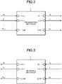
- FIG. 2 is a diagram illustrating an example of the input ports and the output ports of the transmitting BM circuit 1 of the present embodiment. As illustrated in FIG.
- the transmitting BM circuit 1 includes input ports 11-1 to 11-M(where M is an integer equal to or greater than two) and output ports 12-1 to 12-N (where N is an integer equal to or greater than two).
- the input ports 11-1 to 11-M are an example of a plurality of input ports.
- the output ports 12-1 to 12-N are an example of a plurality of output ports.
- the number of input ports, i.e., M corresponds to the maximum number of the transmission signals that can be multiplexed by the communication device 100-1.
- the input signals to, and the output signals from, the transmitting BM circuit 1 will be described later.
- the plurality of second transmission signals output from the individual output ports 12-1 to 12-N of the transmitting BM circuit 1 are each referred to also as transmission OAM signal.
- the plurality of transmission OAM signals output from the transmitting BM circuit 1 are input to the UCA 4 via the separation circuit 3.
- the separation circuit 3 will be described later.
- the UCA 4 emits the transmission OAM signals input from the transmitting BM circuit 1, in the form of a radio wave.
- the UCA 4 includes a plurality of annularly arranged antenna elements.
- the UCA 4 includes the same number of the antenna elements as the number of the output ports of the transmitting BM circuit 1.
- the transmitting BM circuit 1 of the communication device 100-1 provides phase rotations for one or more transmission signals, after which the transmission signals thus provided with the phase rotations are transmitted as a radio wave from the UCA 4.
- the one or more transmission signals can be thus transmitted as an OAM wave.
- the UCA 4 included in the communication device 100-1 of the present embodiment is a transceiver antenna used in both transmission and reception. That is, the UCA 4 is a dual-purpose uniform array antenna, which serves as both a transmission uniform array antenna and a reception uniform array antenna.
- the UCA 4 receives an OAM-multiplexed signal as a radio wave from the communication device 100-2 configured similarly to the communication device 100-1.
- the UCA 4 outputs the received signal to the separation circuit 3.
- the communication device 100-1 is capable of performing transmission and reception simultaneously using the same frequency
- the UCA 4, which is the transceiver antenna is capable of simultaneously transmitting a radio wave and receiving a radio wave.
- a transmission line connected to the UCA 4 to carry both a signal received by the UCA 4 and a transmission OAM signal.
- the separation circuit 3 separates a traveling wave and a reflected wave on the transmission line to thereby separate the signal received by the UCA 4 and the transmission OAM signal from each other.
- the separation circuit 3 outputs, to the UCA 4, the transmission OAM signal thus separated from the UCA-received signal.
- the separation circuit 3 subtracts a replica of an interference signal from each the signal received by each antenna element of the UCA 4 and separated from the transmission OAM signal, and outputs, to the receiving BM circuit 2, a reception OAM signal that is the signal having the replica subtracted.
- the receiving BM circuit 2 includes a plurality of input ports and a plurality of output ports, and performs a reverse operation of the operation performed by the transmitting BM circuit 1.
- the receiving BM circuit 2 can separate the reception OAM signals that have been OAM multiplexed. That is, this enables the communication device 100-1 to obtain reception signals individually corresponding to the plurality of transmission signals that have been OAM multiplexed in the communication device 100-2.
- FIG. 3 is a diagram illustrating an example of the input ports and the output ports of the receiving BM circuit 2 of the present embodiment. As illustrated in FIG. 3 , the receiving BM circuit 2 includes input ports 22-1 to 22-N, and output ports 21-1 to 21-M.
- FIG. 4 is a diagram illustrating an example configuration of the separation circuit 3 and of the UCA 4 of the present embodiment.
- the separation circuit 3 includes directional couplers 5-1 to 5-N, a first interference cancellation circuit 6, and a second interference cancellation circuit 7.
- the UCA 4 includes antenna elements 41-1 to 41-N.
- Each of the transmission OAM signals output from the respective output ports 12-1 to 12-N of the transmitting BM circuit 1 is input to the corresponding one of the directional couplers 5-1 to 5-N, and also input to the first interference cancellation circuit 6.
- Each of the directional couplers 5-1 to 5-N is connected to the corresponding one of the antenna elements 41-1 to 41-N of the UCA 4 through transmission line.
- the transmission line between the antenna element 41-i and the directional coupler 5-i carries the signal received by the antenna element 41-i and the signal output from the directional coupler 5-i to the antenna element 41-i.
- the directional coupler 5-i separates the traveling wave and the reflected wave on the corresponding transmission line to thereby separate the reception signal received by the antenna element 41-i and the transmission OAM signal output to the antenna element 41-i of the UCA 4, and then outputs, to the first interference cancellation circuit 6, the reception signal received by the antenna element 41-i.
- Each of the directional couplers 5-1 to 5-N which is connected to the corresponding one of the antenna elements of the antenna elements 41-1 to 41-N, separates the transmission signal and the reception signal transmitted to and received from the corresponding transceiver antenna.
- the communication device 100-1 of the present embodiment both transmits a first signal to the communication device 100-2, i.e., the communication counterpart, and receives a second signal from the communication device 100-2.
- the first signal is a signal OAM-multiplexed by the communication device 100-1
- the second signal is a signal OAM-multiplexed by the communication device 100-2.
- the communication device 100-1 which receives the second signal, experiences self-interference upon receiving the second signal and transmitting the first signal simultaneously.
- the separation circuit 3 has a function of reducing self-interference to thereby eliminate or reduce the effect of self-interference.
- Examples of self-interference include intra-antenna interference and inter-antenna interference.
- the intra-antenna interference is a phenomenon where a signal transmitted from an antenna element affects that antenna element itself.
- the inter-antenna interference is a phenomenon where a signal transmitted from an antenna element affects another antenna element.
- Intra-antenna interference is caused by, for example, a signal being transmitted from an antenna element and received by that antenna element due to reflection, diffraction, and/or the like.
- intra-antenna interference is interference caused by a signal from a transmitting port of each of the directional couplers 5-1 to 5-N turning around into a receiving port of the directional coupler including that transmitting port because the ports of the individual directional couplers 5-1 to 5-N are insufficiently spaced apart.
- the phrase "intra-antenna" not only means an inside of an antenna element itself, but means a system corresponding to a single antenna element, including the corresponding directional coupler.
- Inter-antenna interference is caused by, for example, a signal being transmitted from an antenna element and received by another antenna element.
- Inter-antenna interference is also caused when leakage between ports of the directional couplers 5-1 to 5-N causes a signal output from an directional coupler to turn around into another directional coupler.
- Intra-antenna interference will be referred to hereinafter as first self-interference
- inter-antenna interference will be referred to hereinafter as second self-interference.
- the first self-interference affects reception operation in a case where an antenna is used in both transmission and reception.
- the second self-interference affects reception operation in both cases where an antenna for transmission and an antenna for reception are separately provided and where an antenna is used in both transmission and reception.
- the UCA 4 is a transceiver antenna, and therefore, the communication device 100-1 is affected by both the first self-interference and the second self-interference.
- the separation circuit 3 of the present embodiment has a function of reducing both the first self-interference and the second self-interference.
- the first interference cancellation circuit 6 cancels the first self-interference from the reception signal input from the directional coupler 5-i. Note that to reduce interference is also referred to hereinafter as to cancel interference. That is, to cancel interference not only means to completely eliminate the interference component, but also means to reduce interference.
- the first interference cancellation circuit 6 outputs, to the second interference cancellation circuit 7, N reception signals having the first self-interference cancelled.
- the transmitting BM circuit 1 includes the input ports 11-1 to 11-M, as illustrated in FIG. 2 .
- Let X 0 to X M-1 denote in a one-to-one correspondence the M transmission signals each input to the corresponding one of the input ports 11-1 to 11-M.
- the input ports 11-1 to 11-M each correspond to one of the OAM modes different from one another.
- x 0 to x N-1 denote, in a one-to-one correspondence
- the transmission OAM signals each output from the corresponding one of the output ports 12-1 to 12-N of the transmitting BM circuit 1.
- Equation (2) the operation performed in the transmitting BM circuit 1 can also be expressed by Equation (2) below using a discrete Fourier transform matrix F.
- the receiving BM circuit 2 includes the input ports 22-1 to 22-N and the output ports 21-1 to 21-M, as illustrated in FIG. 3 .
- Let y 0 to y N-1 denote, in a one-to-one correspondence, the M reception OAM signals each input to the corresponding one of the input ports 22-1 to 22-M of the receiving BM circuit 2.
- Y 0 to Y M-1 denote, in a one-to-one correspondence, the reception signals each output from the corresponding one of the output ports 21-1 to 21-M of the receiving BM circuit 2.
- the reception signal Y m is a reception corresponding to the transmission signal having the m-th OAM mode transmitted from the communication device 100-2.
- Equation (4) the operation performed in the receiving BM circuit 2 can also be expressed by Equation (4) below using the discrete Fourier transform matrix F, where the right superscript H indicates a Hermitian conjugate.
- reception OAM signals u 0 to u N-1 the signals each received by the corresponding one of the antenna elements 41-1 to 41-N are referred to herein as reception OAM signals u 0 to u N-1 in a one-to-one correspondence.
- FIG. 4 omits illustrating the reception OAM signal u 1 and the transmission OAM signal x 1 corresponding to the antenna element 41-2.
- the directional coupler 5-i separates the reception OAM signal u i-1 received by the antenna element 41-i and the transmission OAM signal x i-1 output to the antenna element 41-i, and outputs the reception OAM signal u i-1 to the first interference cancellation circuit 6.
- the first interference cancellation circuit 6 is configured to cancel the first self-interference caused by each of the transmission OAM signals x 0 to x N-1 each included in the corresponding one of the reception OAM signals output from the directional couplers 5-1 to 5-N.
- An interference signal in the first self-interference is referred to hereinafter as first interference signal.
- a first interference signal is an interference signal caused by each of the plurality of transmission signals transmitted from a corresponding one of the antenna elements 41-1 to 41-N that are a plurality of transceiver antenna elements, each of the transmission signals turning around into that corresponding one of the antenna elements 41-1 to 41-N.
- the first interference signal included in the reception OAM signal output from the directional coupler 5-i is the transmission OAM signal x i-1 output from the transmitting BM circuit 1 through the directional coupler 5-i and the antenna element 41-i, input again to the directional coupler 5-i, and output from the directional coupler 5-i.
- the propagation channel of this transmission OAM signal x i-1 is referred to as first interference propagation channel.
- the first interference propagation channel is a loopback channel in which a system providing reception operation of the antenna element 41-i receives the transmission OAM signal x i-1 that should be transmitted from the antenna element 41-i.
- the first interference propagation channel is at least one of: a propagation channel through which the transmission OAM signal x i-1 reflected and/or diffracted by the antenna element 41-i, for example, is received by the same antenna element 41-i; and a leakage propagation channel between ports in the directional coupler 5-i.
- the first interference signal included in the reception OAM signal output from the directional coupler 5-i is the transmission OAM signal x i-1 having an amplitude and a phase that have changed by passing through the first interference propagation channel.
- the communication device 100-1 can therefore generate a replica (reproduction) of the first interference signal by adjusting the amplitude and the phase, of the transmission OAM signal x i-1 in accordance with the transfer function of the first interference propagation channel.
- the first interference cancellation circuit 6 of the separation circuit 3 generates replicas of the N first interference signals corresponding one-to-one to the transmission OAM signals x 0 to x N-1 , and subtracts these replicas from the signals input from the respective directional couplers 5-1 to 5-N. This enables the first interference cancellation circuit 6 to cancel the first self-interference.
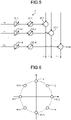
- FIG. 5 is a diagram illustrating an example configuration of the first interference cancellation circuit 6 of the present embodiment.
- the first interference cancellation circuit 6 includes variable amplifiers 61-1 to 61-N, variable phase shifters 62-1 to 62-N, and subtractors 63-1 to 63-N.
- the variable amplifiers 61-1 to 61-N are each an amplifier having a variable gain thereof.
- the variable phase shifters 62-1 to 62-N are each a phase shifter having a variable amount of phase shift.
- Each of the variable amplifiers 61-1 to 61-N amplifies the corresponding one of the amplitudes of the corresponding transmission OAM signals x 0 to x N-1 on the basis of a set gain, and then output the amplified signal to the corresponding one of the variable phase shifters 62-1 to 62-N.
- Each of the variable phase shifters 62-1 to 62-N shifts the phase of the input signal by a set amount of phase shift, and then output the signals having the phase shifted, to the corresponding one of the subtractors 63-1 to 63-N.
- the value of the gain of each of the variable amplifiers 61-1 to 61-N and the amount of phase shift of each of the variable phase shifters 62-1 to 62-N are set in advance on the basis of changes in the amplitude and the phase in the first interference propagation channel.
- the signal output from each of the variable phase shifters 62-1 to 62-N to the corresponding one of the subtractors 63-1 to 63-N is the replica of the first interference signal.
- the transfer function that is, the changes in the amplitude and the phase, in the first interference propagation channel can be calculated on the basis of design values, or be obtained in advance through an experiment or the like.
- Each of the subtractors 63-1 to 63-N subtracts the signal input from the corresponding one of the variable phase shifters 62-1 to 62-N, from the corresponding one of the signals output from the directional couplers 5-1 to 5-N, and outputs the result of subtraction to the second interference cancellation circuit 7.
- the signals output from the subtractors 63-1 to 63-N are referred to herein as reception OAM signals z 0 to z N-1 in a one-to-one correspondence.
- the reception OAM signals z 0 to z N-1 are each a signal obtained by subtraction of the replica of the first interference signal from the reception OAM signal output from the directional coupler 5-i.
- the second interference cancellation circuit 7 will next be described.
- the second interference cancellation circuit 7 generates replicas of interference signals received together with one or more signals transmitted from another device, i.e., the communication device 100-2, on the basis of the transmission signals X 0 to X M-1 , i.e., one or more transmission signals to be transmitted to the other device, and then subtracts the replicas from received signals.
- the second interference cancellation circuit 7 cancels second self-interference, i.e., inter-antenna interference from the reception OAM signals z 0 to z N-1 input from the first interference cancellation circuit 6.
- An interference signal in the second self-interference is referred to hereinafter as second interference signal.
- a second interference signal is an interference signal provided by the transmission OAM signal x i-1 transmitted from the antenna element 41-i and affecting the signal received by an antenna element 41-k (k ⁇ i).
- the reception OAM signal z k-1 is received by the antenna element 41-k, and input to the second interference cancellation circuit 7 via the directional coupler 5-k and the first interference cancellation circuit 6.
- the second interference signal included in the reception OAM signal z k-1 is, for example, the transmission OAM signal x i-1 output from the transmitting BM circuit 1 through at least one of: one or more of the directional couplers 5-1 to 5-N; and one or more of the antenna elements 41-1 to 41-N, and output from a port of the directional coupler 5-k, which port is directed toward the first interference cancellation circuit 6.
- This transmission OAM signal x i-1 output from the directional coupler 5-k is then input to the second interference cancellation circuit 7 via the first interference cancellation circuit 6.
- the propagation channel of this transmission OAM signal x i-1 is referred to herein as second interference propagation channel.
- plural ones of the transmission OAM signals x 0 to x N-1 are input to the second interference cancellation circuit 7 through their corresponding second interference propagation channels, and a sum of such plural transmission OAM signals thus input into the second interference cancellation circuit 7 is the second interference signal included in the reception OAM signal z k-1 .
- the second interference propagation channel includes various types of propagation channels.
- One example of the second interference propagation channel is a line-of-sight communication channel in which the transmission OAM signal x i-1 is transmitted as a radio wave from the antenna element 41-i, and is then received by another antenna element, e.g., the antenna element 41-k, without being affected by reflection, diffraction, or the like.
- Another example of the second interference propagation channel is a non-line-of-sight communication channel in which a transmission signal is affected by reflection, diffraction, and/or the like, and is then received by a receiving antenna.
- the second interference signal is the transmission OAM signal x i-1 that has passed through the line-of-sight communication channel providing no attenuation due to reflection, diffraction, and/or the like.
- the second interference cancellation circuit 7 of the present embodiment treats the transmission OAM signal x i-1 having passed through the line-of-sight communication channel, as the second interference signal, and subtracts the replica of that second interference signal from the reception OAM signal z k-1 to thereby cancel the second self-interference.
- the transmission OAM signals x 0 to x N-1 each included in the corresponding one of the reception OAM signals z 0 to z N-1 and having through a line-of-sight communication channel can be expressed by Equation (5) below, where y v n of the left-hand side of Equation (5) represents a corresponding one of the transmission OAM signals x 0 to x N-1 that is included in the reception OAM signal z n and has passed through a line-of-sight communication channel.
- the hacek mark, or the wedge mark, in the equation is expressed by a superscript v in the text description.
- an element h k,l represents an impulse response in the line-of-sight communication channel between the antenna element 41-(l+1) and the antenna element 41-(k+1).
- Equation (6) The element h k,l can be expressed by Equation (6) below.
- Equation (6) shows that h k,l depends on the propagation distance between antenna elements.
- the UCA 4 has the antenna elements 41-1 to 41-N circumferentially equidistantly arranged.
- each of the antenna elements 41-1 to 41-N serves as both a transmitting antenna element and a receiving antenna element. That is, the antenna elements 41-1 to 41-N are each a transceiver antenna element.
- FIG. 6 is a diagram illustrating an example arrangement of the antenna elements 41-1 to 41-N of the present embodiment. The example illustrated in FIG. 6 is where N is 8. As illustrated in FIG. 6 , the antenna elements 41-1 to 41-8 are annularly arranged at equal angular spacings on the same plane.
- the antenna elements 41-1 to 41-8 are annularly arranged at the equal angular spacings on the same plane, propagation distances from one of the antenna elements 41-1 to 41-8 to the other ones of the antenna elements 41-1 to 41-8 remain the same regardless of whether which of the antenna elements 41-1 to 41-8 is that one antenna element.
- FIG. 7 is a diagram illustrating the propagation distances between the antenna element 41-1 and the other individual antenna elements 41-2 to 41-8.
- the antenna element 41-1 is a first antenna element of the present embodiment.
- FIG. 8 is a diagram illustrating the propagation distances between the antenna element 41-2 and the other individual antenna elements 41-1 and 41-3 to 41-8.
- the antenna element 41-2 is a second antenna element next to the first antenna element.
- FIGS. 8 and 7 illustrate propagation distances as the lengths of the arrows from the origins, i.e., the antenna element 41-1 or 41-2, to the other antenna elements.
- FIG. 7 illustrates the propagation distance between the antenna element 41-1 and the antenna element 41-2 by the length of the arrow from the antenna element 41-1 to the antenna element 41-2.
- FIGS. 7 and 8 are different in the reference numerals denoting the antenna elements that are the origins of the arrows and the ends of the arrows
- the antenna element that is the origin of the arrow of one of FIGs. 7 and 8 is rotated into agreement with the antenna element that is the origin of the arrow of the other of FIGs. 7 and 8 , such that the arrows of FIG. 7 agree with the arrows of FIG. 8 .
- the seven propagation distances from one antenna element of the antenna elements 41-1 to 41-8 to the other antenna elements of the antenna elements 41-1 to 41-8 will have same propagation distance values even when the origin antenna element changes.
- Equation (7) the propagation channel matrix generated on the basis of the propagation distances of direct waves between each of the antenna elements 41-1 to 41-8 and each of the antenna elements 41-1 to 41-8, i.e., the matrix in the right-hand side of Equation (5), is said to have cyclic symmetry.
- Equation (8) a matrix H c representing the line-of-sight communication channel.
- H C h 0 h 1 ⁇ h N ⁇ 1 h N ⁇ 1 h 0 ⁇ h N ⁇ 2 ⁇ ⁇ ⁇ ⁇ h 1 h 2 h N ⁇ 1 h 0
- Equation (9) Since a circulant matrix is diagonalizable using a discrete Fourier transform matrix, a diagonal matrix H D can be obtained as shown by Equation (9) below.
- Equation (10) the second interference signals.
- Equation (10) shows that multiplication of the transmission signals X0 to XM-1 by the diagonal matrix HD and subsequent application of discrete Fourier transform to the result of the multiplication yields the second interference signals.
- the diagonal matrix HD can be calculated in accordance with the propagation distances of the second interference propagation channels.
- the second interference cancellation circuit 7 can generate replicas of the second interference signals by changing the amplitudes and the phases of the individual transmission signals X0 to XM-1 in accordance with the matrix corresponding to the second interference propagation channels, and then applying discrete Fourier transform to the result of changing the amplitudes and the phases.
- the second interference cancellation circuit 7 generates replicas of the second interference signals on the basis of: the propagation channel matrix generated on the basis of the propagation distances of direct waves between each of the antenna elements 41-1 to 41-N and each of the antenna elements 41-1 to 41-N; and the transmission signals X0 to XM-1.
- the propagation channel matrix can be calculated on the basis of the propagation distances of direct waves, that is, design values, or be generated by measurement through an experiment.
- the propagation channel matrix can be obtained by transmitting a test signal from one of the antenna elements and allowing the individual antenna elements to receive the signal. Since, described above, the operation performed in a Butler matrix circuit is similar to discrete Fourier transform, it becomes possible to cancel second self-interference with a simple circuit configuration as the second interference cancellation circuit 7 performs discrete Fourier transform using a Butler matrix circuit.
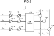
- FIG. 9 is a diagram illustrating an example configuration of the second interference cancellation circuit 7 of the present embodiment.
- the second interference cancellation circuit 7 includes variable amplifiers 71-1 to 71-M, variable phase shifters 72-1 to 72-M, a Butler matrix circuit (hereinafter referred to, using an abbreviation, as BM circuit) 73, and subtractors 74-1 to 74-N.
- BM circuit Butler matrix circuit
- the number M is the maximum number of transmission signals that can be OAM multiplexed, and one or more of practically input transmission signals X 0 to X M-1 suffices. It is therefore only required that one or more of the variable amplifiers 71-1 to 71-M adjust the amplitudes of the individual transmission signals X 0 to X M-1 that are one or more first transmission signals. Also, it is only required that one or more of the variable phase shifters 72-1 to 72-M adjust the phases of the individual transmission signals X 0 to X M-1 having the amplitudes adjusted by the one or more of the variable amplifiers 71-1 to 71-M.
- variable amplifiers 71-1 to 71-M are each an amplifier having a variable gain thereof.
- the variable phase shifters 72-1 to 72-M are each a phase shifter having a variable amount of phase shift.
- Each of the variable amplifiers 71-1 to 71-M has its gain set in accordance with the corresponding element of the diagonal matrix H D .
- Each of the variable phase shifters 72-1 to 72-M has its amount of phase shift set in accordance with the corresponding element of the diagonal matrix H D .
- Each of the variable amplifiers 71-1 to 71-M amplifies the amplitude of the corresponding one of the transmission signals X 0 to X M-1 on the basis of the set gain, and outputs the amplified signal to the corresponding one of the variable phase shifters 72-1 to 72-M.
- Each of the variable phase shifters 72-1 to 72-M shifts the phase of the input signal, by the set amount of phase shift, and outputs, to the BM circuit 73, the signal having the phase shifted.
- the BM circuit 73 includes M input ports and N output ports.
- the BM circuit 73 can use a circuit having the same configuration as the configuration of the transmitting BM circuit 1.
- the BM circuit 73 performs an operation similar to discrete Fourier transform on M signals input from the individual variable phase shifters 72-1 to 72-M, generates N signals, and outputs each of the N signals to the corresponding one of the subtractors 74-1 to 74-N.
- the signals output from the BM circuit 73 to the subtractors 74-1 to 74-N are replicas of the second interference signals.
- the BM circuit 73 generates replicas of the second interference signals by providing the phases for one or more of the transmission signals X 0 to X M-1 having the amplitudes adjusted by one or more of the variable phase shifters 72-1 to 72-M.
- Each of the subtractors 74-1 to 74-N subtracts the replica of the second interference signal from the corresponding one of the reception OAM signals z 0 to z N-1 , and outputs, to the receiving BM circuit 2, the results of the subtraction as the reception OAM signals y 0 to y N-1 .
- the configurations of the first interference cancellation circuit 6 and of the second interference cancellation circuit 7 are not limited to the configurations in the foregoing example.
- At least one of the first interference cancellation circuit 6 and the second interference cancellation circuit 7 can be implemented in software. That is, at least one of the first interference cancellation circuit 6 and the second interference cancellation circuit 7 can be implemented by execution of a program describing an operation of at least one of the first interference cancellation circuit 6 and the second interference cancellation circuit 7.
- the second interference signals are generated using the variable amplifiers 71-1 to 71-M, the variable phase shifters 72-1 to 72-M, and the BM circuit 73, as illustrated in FIG. 9 , it becomes possible to generate the interference signals with a simple circuit configuration.
- the communication device 100-1 can include only one of the first interference cancellation circuit 6 and the second interference cancellation circuit 7. Of the first interference cancellation circuit 6 and the second interference cancellation circuit 7, the communication device 100-1 only includes the second interference cancellation circuit 7, in which case the second interference cancellation circuit 7 serves as the interference cancellation circuit. Alternatively, in a case in which the communication device 100-1 includes the first interference cancellation circuit 6 and the second interference cancellation circuit 7, the first interference cancellation circuit 6 and the second interference cancellation circuit 7 can be considered a single interference cancellation circuit.
- variable amplifiers 61-1 to 61-N and the variable phase shifters 62-1 to 62-N define an interference signal generation circuit in the first interference cancellation circuit 6.
- variable amplifiers 71-1 to 71-M, the variable phase shifters 72-1 to 72-M, and the BM circuit 73 define an interference signal generation circuit in the second interference cancellation circuit 7.
- the communication device 100-1 which both transmits a first signal to a communication counterpart and receives a second signal from the communication counterpart, with an OAM-using communication scheme, includes an interference signal generation circuit.
- the interference signal generation circuit generates a replica of an interference signal caused by the first signal, on the basis of: a transmission OAM signal that is the first signal; or on a transmission signal from which the transmission OAM signal originates. This enables the communication device 100-1 to generate a replica of an interference signal caused by the first signal.
- the communication device 100-1 then subtracts the replica of the interference signal from a reception OAM signal.
- the communication device 100-1 can reduce interference.
- FIG. 10 is a diagram illustrating an example configuration of a communication device according to a second embodiment of the present invention.
- the first embodiment has been described giving the example in which the antenna is used for both transmission and reception.
- the present embodiment will be described giving an example that uses an antenna for transmission and an antenna for reception, separately.
- a communication device 100a-1 of the present embodiment includes the transmitting BM circuit 1 similar to that of the first embodiment, the receiving BM circuit 2 similar to that of the first embodiment, an interference cancellation circuit 8, a transmitting UCA 9, and a receiving UCA 10.
- FIG. 10 also illustrates a communication device 100a-2, which is the communication counterpart of the communication device 100a-1.
- the communication device 100a-2 is configured similarly to the communication device 100a-1.
- the communication device 100a-1 both transmits a first signal to the communication device 100a-2, which is the communication counterpart, and receives a second signal from the communication counterpart.
- Elements each having a function similar to the function of the first embodiment are designated by the same reference characters as used in the first embodiment, and description thereof will therefore be omitted. Differences from the first embodiment will be primarily described below.
- the transmitting UCA 9 and the receiving UCA 10 each include a plurality of antenna elements that are circumferentially equidistantly arranged.
- a transmission OAM signal output from the transmitting BM circuit 1 is input to the transmitting UCA 9, and is emitted as a radio wave from the transmitting UCA 9.
- the communication device 100a-1 which includes an antenna for transmission and an antenna for reception, separately, eliminates the necessity of separating a transmission signal and a reception signal, using the directional couplers 5-1 to 5-N as performed in the first embodiment.
- the communication device 100a-1 does not include the separation circuit 3.
- the communication device 100a-1 includes the interference cancellation circuit 8 downstream of the receiving UCA 10 to cancel, from the reception signals, interference caused by the first signals that are signals transmitted from the transmitting UCA 9.
- the signals received by the receiving UCA 10 are input to the interference cancellation circuit 8.
- FIG. 11 is a diagram illustrating an example configuration of the interference cancellation circuit 8 of the present embodiment.
- the communication device 100a-1 does not include the directional couplers 5-1 to 5-N, it is not necessary to take into consideration a signal turning around between transmitting and receiving ports of each of the directional couplers 5-1 to 5-N. Of the first self-interference and the second self-interference described in the first embodiment, therefore, the first self-interference need not be taken into consideration in the present embodiment.
- second self-interference occurs in which a signal transmitted from a certain antenna element affects another antenna element.
- the second self-interference of the present embodiment is not interference within the same UCA 4 as in the first embodiment, but interference between the transmitting UCA 9 and the receiving UCA 10.
- the method of calculating a propagation distance between antenna elements that should be considered differs partly from the method of the first embodiment, but the self-interference can be canceled using a method similar to the method of cancellation of the second self-interference of the first embodiment.
- the interference cancellation circuit 8 includes variable amplifiers 81-1 to 81-M, variable phase shifters 82-1 to 82-M, a Butler matrix circuit (hereinafter referred to as BM circuit) 83, and subtractors 84-1 to 84-N.
- the variable amplifiers 81-1 to 81-M are each an amplifier having a variable gain thereof.
- the variable phase shifters 82-1 to 82-M are each a phase shifter having a variable amount of phase shift.
- the diagonal matrix H D can be calculated also in the present embodiment, taking a line-of-sight communication channel into consideration as in the first embodiment.
- the transmitting UCA 9 and the receiving UCA 10 are separately provided in the present embodiment, the antenna elements included in the transmitting UCA 9 and the antenna elements included in the receiving UCA 10 are concentrically arranged, such that the propagation distances can be expressed circularly, as in the first embodiment.
- FIG. 12 is a diagram illustrating an example configuration of the transmitting UCA 9 and the receiving UCA 10 of the present embodiment.
- the transmitting UCA 9 and the receiving UCA 10 each include N antenna elements, where N is eight.
- the transmitting UCA 9 includes antenna elements 91-1 to 91-8 that are an example of a plurality of transmitting antenna elements.
- the receiving UCA 10 includes antenna elements 101-1 to 101-8 that are an example of a plurality of receiving antenna elements.
- the antenna elements 91-1 to 91-8 are equidistantly circumferentially arranged on a first circle.
- the antenna elements 101-1 to 101-8 are equidistantly circumferentially arranged on the first circle on which the antenna elements 91-1 to 91-8 are arranged.
- the antenna element 91-1 is disposed between the antenna element 101-1 and the antenna element 101-2.
- the antenna elements 101-1 to 101-8 are each disposed between two adjacent antenna elements of the antenna elements 91-1 to 91-8 in an equally spaced relation to those two transmitting antenna elements.
- the antenna element 91-1 is disposed in such a manner that the circumferential spacing between the antenna element 91-1 and the antenna element 101-1 is equal to the circumferential spacing between the antenna element 91-1 and the antenna element 101-2.
- the plurality of propagation distances from the antenna element 91-1 to the individual antenna elements 101-1 to 101-8 are equal to the plurality of propagation distances from the antenna element 91-2 to the individual antenna elements 101-1 to 101-8 though the corresponding antenna elements are denoted by different reference numerals.
- the propagation distances can be expressed circularly as in the first embodiment. That is, the element h k,l of the matrix of Equation (5) of the first embodiment is applied to the line-of-sight communication channel from the antenna element 91-(l+1) to the antenna element 101-(k+1), thereby enabling the matrix representing the line-of-sight communication channels to be expressed using a circulant matrix as in the first embodiment.
- the diagonal elements of the matrix of Equation (5) in the present embodiment are associated with the case in which the antenna element transmitting a signal differs from the antenna element receiving the signal, and the diagonal elements are therefore not zero.
- the diagonal matrix H D can be calculated also in the present embodiment using a method similar to the method of the first embodiment.
- Each of the variable amplifiers 81-1 to 81-M has its gain set in accordance with the corresponding element of the diagonal matrix H D .
- Each of the variable phase shifters 82-1 to 82-M has its amount of phase shift set in accordance with the corresponding element of the diagonal matrix H D .
- Each of the variable amplifiers 81-1 to 81-M amplifies the amplitude of the corresponding one of the transmission signals X 0 to X M-1 on the basis of the set gain, and outputs the amplified signal to the corresponding one of the variable phase shifters 82-1 to 82-M.
- Each of the variable phase shifters 82-1 to 82-M shifts the phase of the input signal by the set amount of phase shift, and outputs, to the BM circuit 83, the signal having the phase shifted.
- the BM circuit 83 includes M input ports and N output ports.
- the BM circuit 83 performs an operation similar to discrete Fourier transform on M signals input from the individual variable phase shifters 82-1 to 82-M, generates N signals, and outputs each of the N signals to the corresponding one of the subtractors 84-1 to 84-N.
- the signals output from the BM circuit 83 to the subtractors 84-1 to 84-N are replicas of interference signals of the present embodiment.
- Each of the subtractors 84-1 to 84-N subtracts the replica of the corresponding interference signal from the corresponding one of the reception OAM signals v 0 to v N-1 input from the individual antenna elements 101-1 to 101-N, and outputs, to the receiving BM circuit 2, the results of subtraction as the reception OAM signals y 0 to y N-1 .
- variable amplifiers 81-1 to 81-M, the variable phase shifters 82-1 to 82-M, and the BM circuit 83 define an interference signal generation circuit.
- the communication device 100a-1 including the UCA for transmission and the UCA for reception separately generates interference signals, using a method similar to the method of generating the second interference signals of the first embodiment.
- This enables the communication device 100a-1 to generate a replica of an interference signal caused by the first signal.
- the antenna elements 91-1 to 91-N of the transmitting UCA 9 and the antenna elements 101-1 to 101-N of the receiving UCA 10 are alternately arranged at equal angular spacings on the same circle.
- variable amplifiers 81-1 to 81-M, the variable phase shifters 82-1 to 82-M, and the BM circuit 83 define an interference signal generation circuit, similarly to the second interference cancellation circuit 7 of the first embodiment, it becomes possible to generate an interference signal with a simple circuit configuration.
- the communication device 100a-1 of the present embodiment is configured similarly to the second embodiment except that the antenna elements of the transmitting UCA 9 and the receiving UCA 10 are arranged differently from those in the second embodiment.
- Elements each having a function similar to the function of the second embodiment are designated by the same reference characters as used in the second embodiment, and description thereof will therefore be omitted. Differences from the second embodiment will be primarily described below.
- the second embodiment has been described giving the example in which the antenna elements 91-1 to 91-N of the transmitting UCA 9 and the antenna elements 101-1 to 101-N of the receiving UCA 10 are arranged at equal angular spacings on the same circle.
- the set of the antenna elements 91-1 to 91-N of the transmitting UCA 9 and the set of the antenna elements 101-1 to 101-N of the receiving UCA 10 are each arranged on a corresponding one of circles having radiuses different from each other.
- FIG. 13 is a diagram illustrating an example arrangement of the antenna elements of each of the transmitting UCA 9 and the receiving UCA 10 of the present embodiment.
- the antenna elements 91-1 to 91-8 are equidistantly circumferentially arranged on a first circle.
- the antenna elements 101-1 to 101-8 are equidistantly circumferentially arranged on a second circle having a radius smaller than the radius of the first circle on which the antenna elements 91-1 to 91-8 are arranged, the second circle being concentric with the first circle.
- the set of the antenna elements 91-1 to 91-8 and the set of the antenna elements 101-1 to 101-8 are each circumferentially arranged on the corresponding one of the concentric circles having different radiuses, in which case the plurality of propagation distances from one of the antenna elements 91-1 to 91-8 of the transmitting UCA 9 to the individual antenna elements 101-1 to 101-8 of the receiving UCA 10 are equal to the plurality of propagation distances from another antenna element of the antenna elements 91-1 to 91-8 of the transmitting UCA 9 to the individual antenna elements 101-1 to 101-8 of the receiving UCA 10, as in the second embodiment.
- the diagonal matrix H D can accordingly be calculated as in the second embodiment.
- the interference cancellation circuit 8 is configured and operates in the same manner as described in the second embodiment except that the gains set in the individual variable amplifiers 81-1 to 81-M and the amounts of phase shift set in the individual variable phase shifters 82-1 to 82-M differ depending on the arrangement of the antenna elements.
- FIG. 14 is a diagram illustrating another example arrangement of the antenna elements of each of the transmitting UCA 9 and the receiving UCA 10 of the present embodiment.
- the antenna elements 91-1 to 91-8 are equidistantly circumferentially arranged on the first circle.
- the antenna elements 101-1 to 101-8 are arranged at equal angular spacings on a second circle having a radius larger than the radius of the first circle on which the antenna elements 91-1 to 91-8 are arranged, the second circle being concentric with the first circle.
- the antenna elements 101-1 to 101-8 are arranged at the equal angular spacings on the concentric circle having the radius larger than the circle on which the antenna elements 91-1 to 91-8 are arranged, in which case the plurality of propagation distances from one of the antenna elements 91-1 to 91-8 of the transmitting UCA 9 to the individual antenna elements 101-1 to 101-8 of the receiving UCA 10 are equal to the plurality of propagation distances from another antenna element of the antenna elements 91-1 to 91-8 of the transmitting UCA 9 to the individual antenna elements 101-1 to 101-8 of the receiving UCA 10, as in the example of FIG. 13 .
- the diagonal matrix H D can accordingly be calculated similarly to the second embodiment.
- the arrangement illustrated in FIG. 12 described in the second embodiment and the arrangements illustrated in FIGS. 13 and 14 described in the present embodiment are each an example of arrangement that allows the line-of-sight communication channels to be represented circularly.
- the interference cancellation method described in the second embodiment is also applicable to, in addition to these example arrangements, arrangements provided that the propagation channel matrix of line-of-sight communication channels can be represented by Equation (7) above as the arrangements allows the line-of-sight communication channels to be represented circularly.
- Equation (7) when the propagation channels between the antenna elements 91-1 to 91-8 of the transmitting UCA 9 and the antenna elements 101-1 to 101-8 of the receiving UCA 10 satisfy the relationship represented by Equation (7) above, those propagation channels are said to have cyclic symmetry.
- the set of the antenna elements 91-1 to 91-N of the transmitting UCA 9 and the set of the antenna elements 101-1 to 101-N of the receiving UCA 10 are each circumferentially arranged on the corresponding one of the concentric circles having the different radiuses. This configuration can provide an advantage similar to the advantage provided in the second embodiment.
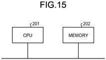
- FIG. 15 is a diagram illustrating an example configuration of processing circuitry in a case in which the processing circuitry of each embodiment includes a CPU.
- the processing circuitry includes a CPU 201 and a memory 202.
- the operation of this at least one circuit is described as a program.
- this at least one circuit is then implemented by the CPU 201 executing the program stored in the memory 202.
- This program can be provided in a program storage medium or by a communication medium.
- the circuits described in the foregoing embodiments can be implemented partly in dedicated hardware and partly in the processing circuitry illustrated in FIG. 15 .
- this program causes the communication device 100-1 or the communication device 100a-1 to perform a first step of generating a replica of an interference signal received together with one or more signals transmitted from another device, on the basis of one or more signals to be transmitted to the another device, and a second step of subtracting the replica from a received signal.
- At least one of the interference signal generation circuits included in the first interference cancellation circuit 6 and in the second interference cancellation circuit 7 described in the first embodiment can be implemented in dedicated hardware or implemented in the processing circuitry illustrated in FIG. 15 .
- the interference signal generation circuit included in the interference cancellation circuit 8 described in the second embodiment can be implemented in dedicated hardware or implemented in the processing circuitry illustrated in FIG. 15 .
Landscapes
- Engineering & Computer Science (AREA)
- Signal Processing (AREA)
- Computer Networks & Wireless Communication (AREA)
- Transceivers (AREA)
- Variable-Direction Aerials And Aerial Arrays (AREA)
- Noise Elimination (AREA)
- Radio Transmission System (AREA)
Abstract
Description
- The present invention relates to a communication device to perform communication in a full-duplex mode using orbital angular momentum, an interference signal generation circuit, a control circuit, an interference cancellation method, and a program storage medium.
- Attention has been directed to a wireless communication system that uses a new spatial multiplexing transmission scheme of orbital angular momentum (OAM). OAM is a type of physical quantity that represents a state of a radio wave in terms of a state of rotation of the phase on a plane perpendicular to the travelling direction. In wireless communication using the OAM, a radio wave is generated in such a manner as to provide a helical equiphase surface relative to the travel direction. The thus generated radio wave is called an OAM wave. The number of rotations of the phase of an OAM wave per wavelength is called an OAM mode. An OAM wave transmitted from a transmitting device is receivable by a receiving device that supports the same OAM mode as the OAM mode of the transmitted OAM wave. Since OAM waves having different OAM modes are orthogonal to one another, combining the plurality of OAM waves having the different OAM modes enables spatial division multiplexing (SDM) transmission. Spatial division multiplexing using the plurality of OAM waves having the different OAM modes is called OAM multiplexing. A receiving device separates signals OAM-multiplexed by a transmitting device, into signals in correspondence to the OAM modes used in the OAM multiplexing.
- Among various methods of generating an OAM wave, a method using a uniform circular array (UCA) antenna is drawing great attention. This is because generating an OAM wave, using a UCA antenna enables transmitting and receiving OAM waves having various OAM modes, and thus provides wide application. In the case of OAM multiplexing using a UCA antenna, for example, a Butler matrix circuit provides each of transmission signals assigned to different OAM modes different with a phase rotation corresponding to the OAM mode of the transmission signal. These transmission signals subjected to the phase rotations are combined together, and the resulting signal is emitted as a radio wave from the UCA antenna.
- A full-duplex wireless communication system using OAM has recently been proposed. Wireless communication using OAM utilizes the orthogonality of OAM multiplexing to thereby achieve a full-duplex wireless communication system capable of performing transmission and reception simultaneously using the same frequency.
Patent Literature 1 discloses a full-duplex wireless communication system that utilizes the orthogonality of OAM multiplexing to perform transmission and reception simultaneously by using different OAM modes in transmission and reception at the same frequency. - Patent Literature 1:
Japanese Patent Application Laid-open No. 2015-207799 - The technology described in
Patent Literature 1 above uses only the orthogonality of OAM multiplexing for separation between transmission and reception. In the case of simultaneous transmission and reception using the same frequency, in some case, a transmission signal transmitted from the communication device turns around into a receiving antenna, thereby causing self-interference. That is, when a first communication device to perform communication using OAM receives a signal from a second communication device, i.e., the communication counterpart, a signal transmitted from the first communication device to the second communication device can act as an interference signal. This interference signal is noise for the first communication device when the first communication device receives a signal. It is therefore desirable to reduce such an interference signal. Unfortunately, the use of only the orthogonality of OAM multiplexing for the separation between the transmission and the reception can fail to reduce the self-interference sufficiently. One possible method for reducing self-interference allows each communication device to generate a replica of the interference signal, and then subtract this replica from a received signal. However,Patent Literature 1 does not discloses any method for generating a replica of an interference signal. - The present invention has been made in view of the foregoing, and it is an object of the present invention to provide a communication device using an OAM-using communication scheme to both transmit a first signal to a communication counterpart and receive a second signal from the communication counterpart, the communication device being capable of generating a replica of an interference signal caused by the first signal.
- To solve the above problem and achieve the object, a communication device according to the present invention is a communication device for wirelessly communicating with another device in a full-duplex mode using orbital angular momentum, the communication device comprising: an interference cancellation circuit to generate a replica of an interference signal received together with one or more signals transmitted from the other device, on a basis of one or more transmission signals to be transmitted to the other device, and to subtract the replica from a received signal.
- A communication device according to the present invention is a communication device using an OAM-using communication scheme to both transmit a first signal to a communication counterpart and receive a second signal from the communication counterpart, and the communication device according to the present invention provides an advantage of generating a replica of an interference signal caused by the first signal.
-
-
FIG. 1 is a diagram illustrating an example configuration of a communication device according to a first embodiment. -
FIG. 2 is a diagram illustrating an example of input ports and output ports of a transmitting BM circuit of the first embodiment. -
FIG. 3 is a diagram illustrating an example of input ports and output ports of a receiving BM circuit of the first embodiment. -
FIG. 4 is a diagram illustrating an example configuration of a separation circuit and of a UCA of the first embodiment. -
FIG. 5 is a diagram illustrating an example configuration of a first interference cancellation circuit of the first embodiment. -
FIG. 6 is a diagram illustrating an example arrangement of antenna elements of the first embodiment. -
FIG. 7 is a diagram illustrating propagation distances between an antenna element that is a first antenna element and the other individual antenna elements of the first embodiment. -
FIG. 8 is a diagram illustrating propagation distances between a second antenna element next to the first antenna element and the other individual antenna elements. -
FIG. 9 is a diagram illustrating an example configuration of a second interference cancellation circuit of the first embodiment. -
FIG. 10 is a diagram illustrating an example configuration of a communication device according to a second embodiment. -
FIG. 11 is a diagram illustrating an example configuration of an interference cancellation circuit of the second embodiment. -
FIG. 12 is a diagram illustrating an example configuration of a transmitting UCA and a receiving UCA of the second embodiment. -
FIG. 13 is a diagram illustrating an example arrangement of the antenna elements of each of a transmitting UCA and a receiving UCA of a third embodiment. -
FIG. 14 is a diagram illustrating another example arrangement of the antenna elements of each of the transmitting UCA and the receiving UCA of the third embodiment. -
FIG. 15 is a diagram illustrating an example configuration of processing circuitry in a case in which the processing circuitry of each embodiment includes a central processing unit (CPU). - A communication device, an interference signal generation circuit, a control circuit, an interference cancellation method, and a program storage medium according to embodiments of the present invention will be described in detail below with reference to the drawings. Note that these embodiments are not intended to limit the scope of this invention.
-
FIG. 1 is a diagram illustrating an example configuration of a communication device according to a first embodiment of the present invention. A communication device 100-1 of the present embodiment includes a transmitting Butler matrix circuit (hereinafter referred to as transmitting BM circuit) 1, a receiving Butler matrix circuit (hereinafter referred to as receiving BM circuit) 2, aseparation circuit 3, and a uniform circular array antenna (hereinafter referred to as UCA) 4.FIG. 1 also illustrates a communication device 100-2, which is the communication counterpart of the communication device 100-1. - The communication device 100-1 wirelessly communicates with another device in a full-duplex mode using orbital angular momentum (OAM). In more detail, the communication device 100-1 performs full-duplex wireless communication, which allows the communication device to perform transmission and reception simultaneously using the same frequency. Note that although the communication device 100-1 is capable of performing transmission and reception simultaneously using the same frequency, the communication device 100-1 does not need to always perform the transmission and the reception simultaneously, and can perform communication switching between a plurality of frequencies, for example. The communication device 100-2 is configured similarly to the communication device 100-1.
- The transmitting
BM circuit 1 includes a plurality of input ports and a plurality of output ports. The transmittingBM circuit 1 provides phase rotations for one or more transmission signals input from at least one of the multiple input ports, the phase rotations being different for the different input ports, and outputs the resulting signals. The transmittingBM circuit 1 provides one or more first transmission signals, which are the one or more transmission signals, with the phases to thereby generate a plurality of second transmission signals.FIG. 2 is a diagram illustrating an example of the input ports and the output ports of the transmittingBM circuit 1 of the present embodiment. As illustrated inFIG. 2 , the transmittingBM circuit 1 includes input ports 11-1 to 11-M(where M is an integer equal to or greater than two) and output ports 12-1 to 12-N (where N is an integer equal to or greater than two). The input ports 11-1 to 11-M are an example of a plurality of input ports. The output ports 12-1 to 12-N are an example of a plurality of output ports. The number of input ports, i.e., M, corresponds to the maximum number of the transmission signals that can be multiplexed by the communication device 100-1. The input signals to, and the output signals from, the transmittingBM circuit 1 will be described later. The plurality of second transmission signals output from the individual output ports 12-1 to 12-N of the transmittingBM circuit 1 are each referred to also as transmission OAM signal. - The plurality of transmission OAM signals output from the transmitting
BM circuit 1 are input to theUCA 4 via theseparation circuit 3. Theseparation circuit 3 will be described later. TheUCA 4 emits the transmission OAM signals input from the transmittingBM circuit 1, in the form of a radio wave. TheUCA 4 includes a plurality of annularly arranged antenna elements. TheUCA 4 includes the same number of the antenna elements as the number of the output ports of the transmittingBM circuit 1. As described above, the transmittingBM circuit 1 of the communication device 100-1 provides phase rotations for one or more transmission signals, after which the transmission signals thus provided with the phase rotations are transmitted as a radio wave from theUCA 4. The one or more transmission signals can be thus transmitted as an OAM wave. When a plurality of transmission signals is input to the individual input ports of the transmittingBM circuit 1, these transmission signals are OAM multiplexed. The method of OAM multiplexing using the Butler matrix circuit and the UCA is similar to a generally known method, and detailed description thereof will therefore be omitted. - The
UCA 4 included in the communication device 100-1 of the present embodiment is a transceiver antenna used in both transmission and reception. That is, theUCA 4 is a dual-purpose uniform array antenna, which serves as both a transmission uniform array antenna and a reception uniform array antenna. TheUCA 4 receives an OAM-multiplexed signal as a radio wave from the communication device 100-2 configured similarly to the communication device 100-1. TheUCA 4 outputs the received signal to theseparation circuit 3. As described above, the communication device 100-1 is capable of performing transmission and reception simultaneously using the same frequency, and theUCA 4, which is the transceiver antenna, is capable of simultaneously transmitting a radio wave and receiving a radio wave. For this reason, a transmission line connected to theUCA 4 to carry both a signal received by theUCA 4 and a transmission OAM signal. Theseparation circuit 3 separates a traveling wave and a reflected wave on the transmission line to thereby separate the signal received by theUCA 4 and the transmission OAM signal from each other. Theseparation circuit 3 outputs, to theUCA 4, the transmission OAM signal thus separated from the UCA-received signal. In addition, theseparation circuit 3 subtracts a replica of an interference signal from each the signal received by each antenna element of theUCA 4 and separated from the transmission OAM signal, and outputs, to the receivingBM circuit 2, a reception OAM signal that is the signal having the replica subtracted. An operation of theseparation circuit 3 will be described later in detail. - The receiving
BM circuit 2 includes a plurality of input ports and a plurality of output ports, and performs a reverse operation of the operation performed by the transmittingBM circuit 1. Thus, the receivingBM circuit 2 can separate the reception OAM signals that have been OAM multiplexed. That is, this enables the communication device 100-1 to obtain reception signals individually corresponding to the plurality of transmission signals that have been OAM multiplexed in the communication device 100-2.FIG. 3 is a diagram illustrating an example of the input ports and the output ports of the receivingBM circuit 2 of the present embodiment. As illustrated inFIG. 3 , the receivingBM circuit 2 includes input ports 22-1 to 22-N, and output ports 21-1 to 21-M. The input ports 22-1 to 22-N are an example of a plurality of input ports, and the output ports 21-1 to 21-M are an example of a plurality of output ports. The receivingBM circuit 2 includes the same number of the input ports as the number of the output ports of the transmittingBM circuit 1, and the receivingBM circuit 2 incudes the same number of the output ports as the number of the input ports of the transmittingBM circuit 1. The method of separation of OAM-multiplexed signals using the UCA and the Butler matrix circuit is similar to a generally known method, and detailed description thereof will therefore be omitted. - The
separation circuit 3 of the present embodiment will next be described.FIG. 4 is a diagram illustrating an example configuration of theseparation circuit 3 and of theUCA 4 of the present embodiment. As illustrated inFIG. 4 , theseparation circuit 3 includes directional couplers 5-1 to 5-N, a firstinterference cancellation circuit 6, and a secondinterference cancellation circuit 7. TheUCA 4 includes antenna elements 41-1 to 41-N. - Each of the transmission OAM signals output from the respective output ports 12-1 to 12-N of the transmitting
BM circuit 1 is input to the corresponding one of the directional couplers 5-1 to 5-N, and also input to the firstinterference cancellation circuit 6. Each of the directional couplers 5-1 to 5-N is connected to the corresponding one of the antenna elements 41-1 to 41-N of theUCA 4 through transmission line. The directional coupler 5-i (i=1, 2, ..., N) outputs, to the antenna element 41-i of theUCA 4, the transmission OAM signal output from the output port 12-i of the transmittingBM circuit 1. The transmission line between the antenna element 41-i and the directional coupler 5-i carries the signal received by the antenna element 41-i and the signal output from the directional coupler 5-i to the antenna element 41-i. The directional coupler 5-i separates the traveling wave and the reflected wave on the corresponding transmission line to thereby separate the reception signal received by the antenna element 41-i and the transmission OAM signal output to the antenna element 41-i of theUCA 4, and then outputs, to the firstinterference cancellation circuit 6, the reception signal received by the antenna element 41-i. Each of the directional couplers 5-1 to 5-N, which is connected to the corresponding one of the antenna elements of the antenna elements 41-1 to 41-N, separates the transmission signal and the reception signal transmitted to and received from the corresponding transceiver antenna. - Interference cancelling in the present embodiment will now be described. With an OAM-using communication scheme, the communication device 100-1 of the present embodiment both transmits a first signal to the communication device 100-2, i.e., the communication counterpart, and receives a second signal from the communication device 100-2. The first signal is a signal OAM-multiplexed by the communication device 100-1, and the second signal is a signal OAM-multiplexed by the communication device 100-2. In some case, the communication device 100-1, which receives the second signal, experiences self-interference upon receiving the second signal and transmitting the first signal simultaneously. In the present embodiment, the
separation circuit 3 has a function of reducing self-interference to thereby eliminate or reduce the effect of self-interference. - Examples of self-interference include intra-antenna interference and inter-antenna interference. The intra-antenna interference is a phenomenon where a signal transmitted from an antenna element affects that antenna element itself. The inter-antenna interference is a phenomenon where a signal transmitted from an antenna element affects another antenna element. Intra-antenna interference is caused by, for example, a signal being transmitted from an antenna element and received by that antenna element due to reflection, diffraction, and/or the like. Another example of intra-antenna interference is interference caused by a signal from a transmitting port of each of the directional couplers 5-1 to 5-N turning around into a receiving port of the directional coupler including that transmitting port because the ports of the individual directional couplers 5-1 to 5-N are insufficiently spaced apart. Note that the phrase "intra-antenna" not only means an inside of an antenna element itself, but means a system corresponding to a single antenna element, including the corresponding directional coupler. Inter-antenna interference is caused by, for example, a signal being transmitted from an antenna element and received by another antenna element. Inter-antenna interference is also caused when leakage between ports of the directional couplers 5-1 to 5-N causes a signal output from an directional coupler to turn around into another directional coupler.
- Intra-antenna interference will be referred to hereinafter as first self-interference, and inter-antenna interference will be referred to hereinafter as second self-interference. The first self-interference affects reception operation in a case where an antenna is used in both transmission and reception. The second self-interference affects reception operation in both cases where an antenna for transmission and an antenna for reception are separately provided and where an antenna is used in both transmission and reception. In the present embodiment, the
UCA 4 is a transceiver antenna, and therefore, the communication device 100-1 is affected by both the first self-interference and the second self-interference. Thus, theseparation circuit 3 of the present embodiment has a function of reducing both the first self-interference and the second self-interference. - Using the transmission OAM signal input from the output port 12-i of the transmitting
BM circuit 1, the firstinterference cancellation circuit 6 cancels the first self-interference from the reception signal input from the directional coupler 5-i. Note that to reduce interference is also referred to hereinafter as to cancel interference. That is, to cancel interference not only means to completely eliminate the interference component, but also means to reduce interference. The firstinterference cancellation circuit 6 outputs, to the secondinterference cancellation circuit 7, N reception signals having the first self-interference cancelled. - An operation of the present embodiment and details of cancellation of the first self-interference and of cancellation of the second self-interference will next be described. The transmitting
BM circuit 1 includes the input ports 11-1 to 11-M, as illustrated inFIG. 2 . Let X0 to XM-1 denote in a one-to-one correspondence the M transmission signals each input to the corresponding one of the input ports 11-1 to 11-M. The input ports 11-1 to 11-M each correspond to one of the OAM modes different from one another. The transmission signal Xm (m=0, 1, ..., M-1) is referred to herein as the transmission signal of the m-th OAM mode. In addition, let x0 to xN-1 denote, in a one-to-one correspondence, the transmission OAM signals each output from the corresponding one of the output ports 12-1 to 12-N of the transmittingBM circuit 1. The operation performed in the transmittingBM circuit 1 is equivalent to discrete Fourier transform operation, and an n-th transmission OAM signal xn (n=0, 1, ..., N-1) can be expressed by Equation (1) below, where j is the imaginary unit. - [Formula 1]

- Note that the operation performed in the transmitting
BM circuit 1 can also be expressed by Equation (2) below using a discrete Fourier transform matrix F. - [Formula 2]

- The receiving
BM circuit 2 includes the input ports 22-1 to 22-N and the output ports 21-1 to 21-M, as illustrated inFIG. 3 . Let y0 to yN-1 denote, in a one-to-one correspondence, the M reception OAM signals each input to the corresponding one of the input ports 22-1 to 22-M of the receivingBM circuit 2. In addition, let Y0 to YM-1 denote, in a one-to-one correspondence, the reception signals each output from the corresponding one of the output ports 21-1 to 21-M of the receivingBM circuit 2. The operation performed in the receivingBM circuit 2 is equivalent to inverse discrete Fourier transform operation, and a reception signal Ym (m=0, 1, ..., M-1) having an m-th OAM mode can be expressed by Equation (3) below. The reception signal Ym is a reception corresponding to the transmission signal having the m-th OAM mode transmitted from the communication device 100-2. - [Formula 3]

- Note that the operation performed in the receiving
BM circuit 2 can also be expressed by Equation (4) below using the discrete Fourier transform matrix F, where the right superscript H indicates a Hermitian conjugate. - [Formula 4]

- An operation of the
separation circuit 3 will next be described. As illustrated inFIG. 4 , the signals each received by the corresponding one of the antenna elements 41-1 to 41-N are referred to herein as reception OAM signals u0 to uN-1 in a one-to-one correspondence. The N transmission lines, which interconnect each of the antenna elements 41-1 to 41-N and the corresponding one of the directional couplers 5-1 to 5-N, carry individually the reception OAM signals u0 to UN-1 and the transmission OAM signals x0 to xN-1. Note that, for convenience of illustration,FIG. 4 omits illustrating the reception OAM signal u1 and the transmission OAM signal x1 corresponding to the antenna element 41-2. - As described above, the directional coupler 5-i separates the reception OAM signal ui-1 received by the antenna element 41-i and the transmission OAM signal xi-1 output to the antenna element 41-i, and outputs the reception OAM signal ui-1 to the first
interference cancellation circuit 6. The firstinterference cancellation circuit 6 is configured to cancel the first self-interference caused by each of the transmission OAM signals x0 to xN-1 each included in the corresponding one of the reception OAM signals output from the directional couplers 5-1 to 5-N. An interference signal in the first self-interference is referred to hereinafter as first interference signal. A first interference signal is an interference signal caused by each of the plurality of transmission signals transmitted from a corresponding one of the antenna elements 41-1 to 41-N that are a plurality of transceiver antenna elements, each of the transmission signals turning around into that corresponding one of the antenna elements 41-1 to 41-N. - An example of the first interference signal included in the reception OAM signal output from the directional coupler 5-i is the transmission OAM signal xi-1 output from the transmitting
BM circuit 1 through the directional coupler 5-i and the antenna element 41-i, input again to the directional coupler 5-i, and output from the directional coupler 5-i. The propagation channel of this transmission OAM signal xi-1 is referred to as first interference propagation channel. The first interference propagation channel is a loopback channel in which a system providing reception operation of the antenna element 41-i receives the transmission OAM signal xi-1 that should be transmitted from the antenna element 41-i. The first interference propagation channel is at least one of: a propagation channel through which the transmission OAM signal xi-1 reflected and/or diffracted by the antenna element 41-i, for example, is received by the same antenna element 41-i; and a leakage propagation channel between ports in the directional coupler 5-i. The first interference signal included in the reception OAM signal output from the directional coupler 5-i is the transmission OAM signal xi-1 having an amplitude and a phase that have changed by passing through the first interference propagation channel. The communication device 100-1 can therefore generate a replica (reproduction) of the first interference signal by adjusting the amplitude and the phase, of the transmission OAM signal xi-1 in accordance with the transfer function of the first interference propagation channel. - In the present embodiment, the first
interference cancellation circuit 6 of theseparation circuit 3 generates replicas of the N first interference signals corresponding one-to-one to the transmission OAM signals x0 to xN-1, and subtracts these replicas from the signals input from the respective directional couplers 5-1 to 5-N. This enables the firstinterference cancellation circuit 6 to cancel the first self-interference. -
FIG. 5 is a diagram illustrating an example configuration of the firstinterference cancellation circuit 6 of the present embodiment. As illustrated inFIG. 5 , the firstinterference cancellation circuit 6 includes variable amplifiers 61-1 to 61-N, variable phase shifters 62-1 to 62-N, and subtractors 63-1 to 63-N. The variable amplifiers 61-1 to 61-N are each an amplifier having a variable gain thereof. The variable phase shifters 62-1 to 62-N are each a phase shifter having a variable amount of phase shift. Each of the variable amplifiers 61-1 to 61-N amplifies the corresponding one of the amplitudes of the corresponding transmission OAM signals x0 to xN-1 on the basis of a set gain, and then output the amplified signal to the corresponding one of the variable phase shifters 62-1 to 62-N. Each of the variable phase shifters 62-1 to 62-N shifts the phase of the input signal by a set amount of phase shift, and then output the signals having the phase shifted, to the corresponding one of the subtractors 63-1 to 63-N. The value of the gain of each of the variable amplifiers 61-1 to 61-N and the amount of phase shift of each of the variable phase shifters 62-1 to 62-N are set in advance on the basis of changes in the amplitude and the phase in the first interference propagation channel. The signal output from each of the variable phase shifters 62-1 to 62-N to the corresponding one of the subtractors 63-1 to 63-N is the replica of the first interference signal. Note that the transfer function, that is, the changes in the amplitude and the phase, in the first interference propagation channel can be calculated on the basis of design values, or be obtained in advance through an experiment or the like. - Each of the subtractors 63-1 to 63-N subtracts the signal input from the corresponding one of the variable phase shifters 62-1 to 62-N, from the corresponding one of the signals output from the directional couplers 5-1 to 5-N, and outputs the result of subtraction to the second
interference cancellation circuit 7. The signals output from the subtractors 63-1 to 63-N are referred to herein as reception OAM signals z0 to zN-1 in a one-to-one correspondence. The reception OAM signals z0 to zN-1 are each a signal obtained by subtraction of the replica of the first interference signal from the reception OAM signal output from the directional coupler 5-i. - The second
interference cancellation circuit 7 will next be described. The secondinterference cancellation circuit 7 generates replicas of interference signals received together with one or more signals transmitted from another device, i.e., the communication device 100-2, on the basis of the transmission signals X0 to XM-1, i.e., one or more transmission signals to be transmitted to the other device, and then subtracts the replicas from received signals. Specifically, the secondinterference cancellation circuit 7 cancels second self-interference, i.e., inter-antenna interference from the reception OAM signals z0 to zN-1 input from the firstinterference cancellation circuit 6. An interference signal in the second self-interference is referred to hereinafter as second interference signal. A second interference signal is an interference signal provided by the transmission OAM signal xi-1 transmitted from the antenna element 41-i and affecting the signal received by an antenna element 41-k (k≠i). - The reception OAM signal zk-1 is received by the antenna element 41-k, and input to the second
interference cancellation circuit 7 via the directional coupler 5-k and the firstinterference cancellation circuit 6. The second interference signal included in the reception OAM signal zk-1 is, for example, the transmission OAM signal xi-1 output from the transmittingBM circuit 1 through at least one of: one or more of the directional couplers 5-1 to 5-N; and one or more of the antenna elements 41-1 to 41-N, and output from a port of the directional coupler 5-k, which port is directed toward the firstinterference cancellation circuit 6. This transmission OAM signal xi-1 output from the directional coupler 5-k is then input to the secondinterference cancellation circuit 7 via the firstinterference cancellation circuit 6. The propagation channel of this transmission OAM signal xi-1 is referred to herein as second interference propagation channel. In some case, plural ones of the transmission OAM signals x0 to xN-1 are input to the secondinterference cancellation circuit 7 through their corresponding second interference propagation channels, and a sum of such plural transmission OAM signals thus input into the secondinterference cancellation circuit 7 is the second interference signal included in the reception OAM signal zk-1. - The second interference propagation channel includes various types of propagation channels. One example of the second interference propagation channel is a line-of-sight communication channel in which the transmission OAM signal xi-1 is transmitted as a radio wave from the antenna element 41-i, and is then received by another antenna element, e.g., the antenna element 41-k, without being affected by reflection, diffraction, or the like. Another example of the second interference propagation channel is a non-line-of-sight communication channel in which a transmission signal is affected by reflection, diffraction, and/or the like, and is then received by a receiving antenna. A non-line-of-sight communication channel will be subjected not only to distance attenuation dependent on the propagation distance, but also to attenuation in the signal level due to reflection, diffraction, and/or the like. In most cases, accordingly, the second interference signal is the transmission OAM signal xi-1 that has passed through the line-of-sight communication channel providing no attenuation due to reflection, diffraction, and/or the like. Thus, the second
interference cancellation circuit 7 of the present embodiment treats the transmission OAM signal xi-1 having passed through the line-of-sight communication channel, as the second interference signal, and subtracts the replica of that second interference signal from the reception OAM signal zk-1 to thereby cancel the second self-interference. - The transmission OAM signals x0 to xN-1 each included in the corresponding one of the reception OAM signals z0 to zN-1 and having through a line-of-sight communication channel can be expressed by Equation (5) below, where yv n of the left-hand side of Equation (5) represents a corresponding one of the transmission OAM signals x0 to xN-1 that is included in the reception OAM signal zn and has passed through a line-of-sight communication channel. Note that the hacek mark, or the wedge mark, in the equation is expressed by a superscript v in the text description. In addition, an element hk,l represents an impulse response in the line-of-sight communication channel between the antenna element 41-(l+1) and the antenna element 41-(k+1).
- [Formula 5]

- The element hk,l can be expressed by Equation (6) below.
- [Formula 6]

- Note that dk,l represents the propagation distance between the antenna element 41-(l+1) and the antenna element 41-(k+1). Note that although the matrix of Equation (5) includes diagonal elements, that is, elements which correspond to the case in which an antenna element transmitting a signal and an antenna element receiving a signal are the same, the diagonal elements of the matrix of Equation (5) are zero because a propagation distance is zero. In addition, β represents an attenuation ratio and the amount of phase rotation common to all of the antenna elements 41-1 to 41-N, and λ represents the wavelengths of the radio waves transmitted by the antenna elements 41-1 to 41-N. Equation (6) shows that hk,l depends on the propagation distance between antenna elements.
- The
UCA 4 has the antenna elements 41-1 to 41-N circumferentially equidistantly arranged. In the present embodiment, each of the antenna elements 41-1 to 41-N serves as both a transmitting antenna element and a receiving antenna element. That is, the antenna elements 41-1 to 41-N are each a transceiver antenna element.FIG. 6 is a diagram illustrating an example arrangement of the antenna elements 41-1 to 41-N of the present embodiment. The example illustrated inFIG. 6 is where N is 8. As illustrated inFIG. 6 , the antenna elements 41-1 to 41-8 are annularly arranged at equal angular spacings on the same plane. Since the antenna elements 41-1 to 41-8 are annularly arranged at the equal angular spacings on the same plane, propagation distances from one of the antenna elements 41-1 to 41-8 to the other ones of the antenna elements 41-1 to 41-8 remain the same regardless of whether which of the antenna elements 41-1 to 41-8 is that one antenna element. -
FIG. 7 is a diagram illustrating the propagation distances between the antenna element 41-1 and the other individual antenna elements 41-2 to 41-8. The antenna element 41-1 is a first antenna element of the present embodiment.FIG. 8 is a diagram illustrating the propagation distances between the antenna element 41-2 and the other individual antenna elements 41-1 and 41-3 to 41-8. The antenna element 41-2 is a second antenna element next to the first antenna element.FIGS. 8 and 7 illustrate propagation distances as the lengths of the arrows from the origins, i.e., the antenna element 41-1 or 41-2, to the other antenna elements. For example,FIG. 7 illustrates the propagation distance between the antenna element 41-1 and the antenna element 41-2 by the length of the arrow from the antenna element 41-1 to the antenna element 41-2. AlthoughFIGS. 7 and 8 are different in the reference numerals denoting the antenna elements that are the origins of the arrows and the ends of the arrows, the antenna element that is the origin of the arrow of one ofFIGs. 7 and 8 is rotated into agreement with the antenna element that is the origin of the arrow of the other ofFIGs. 7 and 8 , such that the arrows ofFIG. 7 agree with the arrows ofFIG. 8 . The seven propagation distances from one antenna element of the antenna elements 41-1 to 41-8 to the other antenna elements of the antenna elements 41-1 to 41-8 will have same propagation distance values even when the origin antenna element changes. - Thus, the element hk,l can be expressed by Equation (7) below. When the relationship represented by Equation (7) is satisfied, the propagation channel matrix generated on the basis of the propagation distances of direct waves between each of the antenna elements 41-1 to 41-8 and each of the antenna elements 41-1 to 41-8, i.e., the matrix in the right-hand side of Equation (5), is said to have cyclic symmetry.

- Accordingly, the matrix in the right-hand side of Equation (5), i.e., a matrix Hc representing the line-of-sight communication channel, can be expressed by the circulant matrix given in Equation (8) below.

- Since a circulant matrix is diagonalizable using a discrete Fourier transform matrix, a diagonal matrix HD can be obtained as shown by Equation (9) below.

- Thus, the second interference signals can be expressed by Equation (10) below. [Formula 10]

- Equation (10) shows that multiplication of the transmission signals X0 to XM-1 by the diagonal matrix HD and subsequent application of discrete Fourier transform to the result of the multiplication yields the second interference signals. From Equations (5) to (8), the diagonal matrix HD can be calculated in accordance with the propagation distances of the second interference propagation channels. The second
interference cancellation circuit 7 can generate replicas of the second interference signals by changing the amplitudes and the phases of the individual transmission signals X0 to XM-1 in accordance with the matrix corresponding to the second interference propagation channels, and then applying discrete Fourier transform to the result of changing the amplitudes and the phases. That is, the secondinterference cancellation circuit 7 generates replicas of the second interference signals on the basis of: the propagation channel matrix generated on the basis of the propagation distances of direct waves between each of the antenna elements 41-1 to 41-N and each of the antenna elements 41-1 to 41-N; and the transmission signals X0 to XM-1. Note that the propagation channel matrix can be calculated on the basis of the propagation distances of direct waves, that is, design values, or be generated by measurement through an experiment. For example, the propagation channel matrix can be obtained by transmitting a test signal from one of the antenna elements and allowing the individual antenna elements to receive the signal. Since, described above, the operation performed in a Butler matrix circuit is similar to discrete Fourier transform, it becomes possible to cancel second self-interference with a simple circuit configuration as the secondinterference cancellation circuit 7 performs discrete Fourier transform using a Butler matrix circuit. -
FIG. 9 is a diagram illustrating an example configuration of the secondinterference cancellation circuit 7 of the present embodiment. As illustrated inFIG. 9 , the secondinterference cancellation circuit 7 includes variable amplifiers 71-1 to 71-M, variable phase shifters 72-1 to 72-M, a Butler matrix circuit (hereinafter referred to, using an abbreviation, as BM circuit) 73, and subtractors 74-1 to 74-N. - Note that, as described above, the number M is the maximum number of transmission signals that can be OAM multiplexed, and one or more of practically input transmission signals X0 to XM-1 suffices. It is therefore only required that one or more of the variable amplifiers 71-1 to 71-M adjust the amplitudes of the individual transmission signals X0 to XM-1 that are one or more first transmission signals. Also, it is only required that one or more of the variable phase shifters 72-1 to 72-M adjust the phases of the individual transmission signals X0 to XM-1 having the amplitudes adjusted by the one or more of the variable amplifiers 71-1 to 71-M.
- The variable amplifiers 71-1 to 71-M are each an amplifier having a variable gain thereof. The variable phase shifters 72-1 to 72-M are each a phase shifter having a variable amount of phase shift. Each of the variable amplifiers 71-1 to 71-M has its gain set in accordance with the corresponding element of the diagonal matrix HD. Each of the variable phase shifters 72-1 to 72-M has its amount of phase shift set in accordance with the corresponding element of the diagonal matrix HD. Each of the variable amplifiers 71-1 to 71-M amplifies the amplitude of the corresponding one of the transmission signals X0 to XM-1 on the basis of the set gain, and outputs the amplified signal to the corresponding one of the variable phase shifters 72-1 to 72-M. Each of the variable phase shifters 72-1 to 72-M shifts the phase of the input signal, by the set amount of phase shift, and outputs, to the BM circuit 73, the signal having the phase shifted.
- Similarly to the transmitting
BM circuit 1, the BM circuit 73 includes M input ports and N output ports. The BM circuit 73 can use a circuit having the same configuration as the configuration of the transmittingBM circuit 1. The BM circuit 73 performs an operation similar to discrete Fourier transform on M signals input from the individual variable phase shifters 72-1 to 72-M, generates N signals, and outputs each of the N signals to the corresponding one of the subtractors 74-1 to 74-N. The signals output from the BM circuit 73 to the subtractors 74-1 to 74-N are replicas of the second interference signals. That is, the BM circuit 73 generates replicas of the second interference signals by providing the phases for one or more of the transmission signals X0 to XM-1 having the amplitudes adjusted by one or more of the variable phase shifters 72-1 to 72-M. Each of the subtractors 74-1 to 74-N subtracts the replica of the second interference signal from the corresponding one of the reception OAM signals z0 to zN-1, and outputs, to the receivingBM circuit 2, the results of the subtraction as the reception OAM signals y0 to yN-1. - Note that the configurations of the first
interference cancellation circuit 6 and of the secondinterference cancellation circuit 7 are not limited to the configurations in the foregoing example. At least one of the firstinterference cancellation circuit 6 and the secondinterference cancellation circuit 7 can be implemented in software. That is, at least one of the firstinterference cancellation circuit 6 and the secondinterference cancellation circuit 7 can be implemented by execution of a program describing an operation of at least one of the firstinterference cancellation circuit 6 and the secondinterference cancellation circuit 7. Note that since the second interference signals are generated using the variable amplifiers 71-1 to 71-M, the variable phase shifters 72-1 to 72-M, and the BM circuit 73, as illustrated inFIG. 9 , it becomes possible to generate the interference signals with a simple circuit configuration. - The present embodiment has been described giving the example in which both the first interference signals and the second interference signals are generated using the first
interference cancellation circuit 6 and the secondinterference cancellation circuit 7 to reduce the effects of both of interference signals. However, the communication device 100-1 can include only one of the firstinterference cancellation circuit 6 and the secondinterference cancellation circuit 7. Of the firstinterference cancellation circuit 6 and the secondinterference cancellation circuit 7, the communication device 100-1 only includes the secondinterference cancellation circuit 7, in which case the secondinterference cancellation circuit 7 serves as the interference cancellation circuit. Alternatively, in a case in which the communication device 100-1 includes the firstinterference cancellation circuit 6 and the secondinterference cancellation circuit 7, the firstinterference cancellation circuit 6 and the secondinterference cancellation circuit 7 can be considered a single interference cancellation circuit. - Note that the variable amplifiers 61-1 to 61-N and the variable phase shifters 62-1 to 62-N define an interference signal generation circuit in the first
interference cancellation circuit 6. In addition, the variable amplifiers 71-1 to 71-M, the variable phase shifters 72-1 to 72-M, and the BM circuit 73 define an interference signal generation circuit in the secondinterference cancellation circuit 7. - As described above, in the present embodiment, the communication device 100-1, which both transmits a first signal to a communication counterpart and receives a second signal from the communication counterpart, with an OAM-using communication scheme, includes an interference signal generation circuit. The interference signal generation circuit generates a replica of an interference signal caused by the first signal, on the basis of: a transmission OAM signal that is the first signal; or on a transmission signal from which the transmission OAM signal originates. This enables the communication device 100-1 to generate a replica of an interference signal caused by the first signal. The communication device 100-1 then subtracts the replica of the interference signal from a reception OAM signal. Thus, the communication device 100-1 can reduce interference.
-
FIG. 10 is a diagram illustrating an example configuration of a communication device according to a second embodiment of the present invention. The first embodiment has been described giving the example in which the antenna is used for both transmission and reception. In contrast, the present embodiment will be described giving an example that uses an antenna for transmission and an antenna for reception, separately. - A
communication device 100a-1 of the present embodiment includes the transmittingBM circuit 1 similar to that of the first embodiment, the receivingBM circuit 2 similar to that of the first embodiment, aninterference cancellation circuit 8, a transmittingUCA 9, and a receivingUCA 10.FIG. 10 also illustrates acommunication device 100a-2, which is the communication counterpart of thecommunication device 100a-1. Thecommunication device 100a-2 is configured similarly to thecommunication device 100a-1. Similarly to the first embodiment, with both using an OAM-using communication scheme, thecommunication device 100a-1 both transmits a first signal to thecommunication device 100a-2, which is the communication counterpart, and receives a second signal from the communication counterpart. Elements each having a function similar to the function of the first embodiment are designated by the same reference characters as used in the first embodiment, and description thereof will therefore be omitted. Differences from the first embodiment will be primarily described below. - Similarly to the
UCA 4 of the first embodiment, the transmittingUCA 9 and the receivingUCA 10 each include a plurality of antenna elements that are circumferentially equidistantly arranged. A transmission OAM signal output from the transmittingBM circuit 1 is input to the transmittingUCA 9, and is emitted as a radio wave from the transmittingUCA 9. In the present embodiment, thecommunication device 100a-1, which includes an antenna for transmission and an antenna for reception, separately, eliminates the necessity of separating a transmission signal and a reception signal, using the directional couplers 5-1 to 5-N as performed in the first embodiment. Thus, thecommunication device 100a-1 does not include theseparation circuit 3. In the present embodiment, thecommunication device 100a-1 includes theinterference cancellation circuit 8 downstream of the receivingUCA 10 to cancel, from the reception signals, interference caused by the first signals that are signals transmitted from the transmittingUCA 9. The signals received by the receivingUCA 10 are input to theinterference cancellation circuit 8. -
FIG. 11 is a diagram illustrating an example configuration of theinterference cancellation circuit 8 of the present embodiment. In the present embodiment, even when a signal transmitted from the transmittingUCA 9 is received by the transmittingUCA 9 due to diffraction, reflection, and/or the like, such a signal has no direct effect on signal reception by the receivingUCA 10. In addition, since thecommunication device 100a-1 does not include the directional couplers 5-1 to 5-N, it is not necessary to take into consideration a signal turning around between transmitting and receiving ports of each of the directional couplers 5-1 to 5-N. Of the first self-interference and the second self-interference described in the first embodiment, therefore, the first self-interference need not be taken into consideration in the present embodiment. - In the present embodiment, second self-interference occurs in which a signal transmitted from a certain antenna element affects another antenna element. However, the second self-interference of the present embodiment is not interference within the
same UCA 4 as in the first embodiment, but interference between the transmittingUCA 9 and the receivingUCA 10. Thus, the method of calculating a propagation distance between antenna elements that should be considered differs partly from the method of the first embodiment, but the self-interference can be canceled using a method similar to the method of cancellation of the second self-interference of the first embodiment. - As illustrated in
FIG. 11 , theinterference cancellation circuit 8 includes variable amplifiers 81-1 to 81-M, variable phase shifters 82-1 to 82-M, a Butler matrix circuit (hereinafter referred to as BM circuit) 83, and subtractors 84-1 to 84-N. The variable amplifiers 81-1 to 81-M are each an amplifier having a variable gain thereof. The variable phase shifters 82-1 to 82-M are each a phase shifter having a variable amount of phase shift. - The diagonal matrix HD can be calculated also in the present embodiment, taking a line-of-sight communication channel into consideration as in the first embodiment. Although the transmitting
UCA 9 and the receivingUCA 10 are separately provided in the present embodiment, the antenna elements included in the transmittingUCA 9 and the antenna elements included in the receivingUCA 10 are concentrically arranged, such that the propagation distances can be expressed circularly, as in the first embodiment. -
FIG. 12 is a diagram illustrating an example configuration of the transmittingUCA 9 and the receivingUCA 10 of the present embodiment. InFIG. 12 , the transmittingUCA 9 and the receivingUCA 10 each include N antenna elements, where N is eight. The transmittingUCA 9 includes antenna elements 91-1 to 91-8 that are an example of a plurality of transmitting antenna elements. The receivingUCA 10 includes antenna elements 101-1 to 101-8 that are an example of a plurality of receiving antenna elements. The antenna elements 91-1 to 91-8 are equidistantly circumferentially arranged on a first circle. The antenna elements 101-1 to 101-8 are equidistantly circumferentially arranged on the first circle on which the antenna elements 91-1 to 91-8 are arranged. - As illustrated in
FIG. 12 , the antenna element 91-1 is disposed between the antenna element 101-1 and the antenna element 101-2. The antenna elements 101-1 to 101-8 are each disposed between two adjacent antenna elements of the antenna elements 91-1 to 91-8 in an equally spaced relation to those two transmitting antenna elements. For example, the antenna element 91-1 is disposed in such a manner that the circumferential spacing between the antenna element 91-1 and the antenna element 101-1 is equal to the circumferential spacing between the antenna element 91-1 and the antenna element 101-2. As a result, the plurality of propagation distances from the antenna element 91-1 to the individual antenna elements 101-1 to 101-8 are equal to the plurality of propagation distances from the antenna element 91-2 to the individual antenna elements 101-1 to 101-8 though the corresponding antenna elements are denoted by different reference numerals. Thus, the propagation distances can be expressed circularly as in the first embodiment. That is, the element hk,l of the matrix of Equation (5) of the first embodiment is applied to the line-of-sight communication channel from the antenna element 91-(l+1) to the antenna element 101-(k+1), thereby enabling the matrix representing the line-of-sight communication channels to be expressed using a circulant matrix as in the first embodiment. Note, however, that the diagonal elements of the matrix of Equation (5) in the present embodiment are associated with the case in which the antenna element transmitting a signal differs from the antenna element receiving the signal, and the diagonal elements are therefore not zero. As described above, although the propagation distances of the present embodiment differ from the propagation distances of the first embodiment, the diagonal matrix HD can be calculated also in the present embodiment using a method similar to the method of the first embodiment. - Each of the variable amplifiers 81-1 to 81-M has its gain set in accordance with the corresponding element of the diagonal matrix HD. Each of the variable phase shifters 82-1 to 82-M has its amount of phase shift set in accordance with the corresponding element of the diagonal matrix HD. Each of the variable amplifiers 81-1 to 81-M amplifies the amplitude of the corresponding one of the transmission signals X0 to XM-1 on the basis of the set gain, and outputs the amplified signal to the corresponding one of the variable phase shifters 82-1 to 82-M. Each of the variable phase shifters 82-1 to 82-M shifts the phase of the input signal by the set amount of phase shift, and outputs, to the BM circuit 83, the signal having the phase shifted.
- Similarly to the BM circuit 73, the BM circuit 83 includes M input ports and N output ports. The BM circuit 83 performs an operation similar to discrete Fourier transform on M signals input from the individual variable phase shifters 82-1 to 82-M, generates N signals, and outputs each of the N signals to the corresponding one of the subtractors 84-1 to 84-N. The signals output from the BM circuit 83 to the subtractors 84-1 to 84-N are replicas of interference signals of the present embodiment. Each of the subtractors 84-1 to 84-N subtracts the replica of the corresponding interference signal from the corresponding one of the reception OAM signals v0 to vN-1 input from the individual antenna elements 101-1 to 101-N, and outputs, to the receiving
BM circuit 2, the results of subtraction as the reception OAM signals y0 to yN-1. - In the present embodiment, the variable amplifiers 81-1 to 81-M, the variable phase shifters 82-1 to 82-M, and the BM circuit 83 define an interference signal generation circuit.
- As described above, in the present embodiment, the
communication device 100a-1 including the UCA for transmission and the UCA for reception separately generates interference signals, using a method similar to the method of generating the second interference signals of the first embodiment. This enables thecommunication device 100a-1 to generate a replica of an interference signal caused by the first signal. The antenna elements 91-1 to 91-N of the transmittingUCA 9 and the antenna elements 101-1 to 101-N of the receivingUCA 10 are alternately arranged at equal angular spacings on the same circle. Since the variable amplifiers 81-1 to 81-M, the variable phase shifters 82-1 to 82-M, and the BM circuit 83 define an interference signal generation circuit, similarly to the secondinterference cancellation circuit 7 of the first embodiment, it becomes possible to generate an interference signal with a simple circuit configuration. - A third embodiment according to the present invention will next be described. The
communication device 100a-1 of the present embodiment is configured similarly to the second embodiment except that the antenna elements of the transmittingUCA 9 and the receivingUCA 10 are arranged differently from those in the second embodiment. Elements each having a function similar to the function of the second embodiment are designated by the same reference characters as used in the second embodiment, and description thereof will therefore be omitted. Differences from the second embodiment will be primarily described below. - The second embodiment has been described giving the example in which the antenna elements 91-1 to 91-N of the transmitting
UCA 9 and the antenna elements 101-1 to 101-N of the receivingUCA 10 are arranged at equal angular spacings on the same circle. In the present embodiment, the set of the antenna elements 91-1 to 91-N of the transmittingUCA 9 and the set of the antenna elements 101-1 to 101-N of the receivingUCA 10 are each arranged on a corresponding one of circles having radiuses different from each other. -
FIG. 13 is a diagram illustrating an example arrangement of the antenna elements of each of the transmittingUCA 9 and the receivingUCA 10 of the present embodiment. The antenna elements 91-1 to 91-8 are equidistantly circumferentially arranged on a first circle. The antenna elements 101-1 to 101-8 are equidistantly circumferentially arranged on a second circle having a radius smaller than the radius of the first circle on which the antenna elements 91-1 to 91-8 are arranged, the second circle being concentric with the first circle. In the present embodiment, the set of the antenna elements 91-1 to 91-8 and the set of the antenna elements 101-1 to 101-8 are each circumferentially arranged on the corresponding one of the concentric circles having different radiuses, in which case the plurality of propagation distances from one of the antenna elements 91-1 to 91-8 of the transmittingUCA 9 to the individual antenna elements 101-1 to 101-8 of the receivingUCA 10 are equal to the plurality of propagation distances from another antenna element of the antenna elements 91-1 to 91-8 of the transmittingUCA 9 to the individual antenna elements 101-1 to 101-8 of the receivingUCA 10, as in the second embodiment. - The diagonal matrix HD can accordingly be calculated as in the second embodiment. The
interference cancellation circuit 8 is configured and operates in the same manner as described in the second embodiment except that the gains set in the individual variable amplifiers 81-1 to 81-M and the amounts of phase shift set in the individual variable phase shifters 82-1 to 82-M differ depending on the arrangement of the antenna elements. -
FIG. 14 is a diagram illustrating another example arrangement of the antenna elements of each of the transmittingUCA 9 and the receivingUCA 10 of the present embodiment. The antenna elements 91-1 to 91-8 are equidistantly circumferentially arranged on the first circle. The antenna elements 101-1 to 101-8 are arranged at equal angular spacings on a second circle having a radius larger than the radius of the first circle on which the antenna elements 91-1 to 91-8 are arranged, the second circle being concentric with the first circle. In the present embodiment, the antenna elements 101-1 to 101-8 are arranged at the equal angular spacings on the concentric circle having the radius larger than the circle on which the antenna elements 91-1 to 91-8 are arranged, in which case the plurality of propagation distances from one of the antenna elements 91-1 to 91-8 of the transmittingUCA 9 to the individual antenna elements 101-1 to 101-8 of the receivingUCA 10 are equal to the plurality of propagation distances from another antenna element of the antenna elements 91-1 to 91-8 of the transmittingUCA 9 to the individual antenna elements 101-1 to 101-8 of the receivingUCA 10, as in the example ofFIG. 13 . The diagonal matrix HD can accordingly be calculated similarly to the second embodiment. - Note that the arrangement illustrated in
FIG. 12 described in the second embodiment and the arrangements illustrated inFIGS. 13 and 14 described in the present embodiment are each an example of arrangement that allows the line-of-sight communication channels to be represented circularly. The interference cancellation method described in the second embodiment is also applicable to, in addition to these example arrangements, arrangements provided that the propagation channel matrix of line-of-sight communication channels can be represented by Equation (7) above as the arrangements allows the line-of-sight communication channels to be represented circularly. Note that when the propagation channels between the antenna elements 91-1 to 91-8 of the transmittingUCA 9 and the antenna elements 101-1 to 101-8 of the receivingUCA 10 satisfy the relationship represented by Equation (7) above, those propagation channels are said to have cyclic symmetry. - As described above, in the present embodiment, the set of the antenna elements 91-1 to 91-N of the transmitting
UCA 9 and the set of the antenna elements 101-1 to 101-N of the receivingUCA 10 are each circumferentially arranged on the corresponding one of the concentric circles having the different radiuses. This configuration can provide an advantage similar to the advantage provided in the second embodiment. - The circuits described in the foregoing embodiments are each processing circuitry, and can each be dedicated hardware, or processing circuitry including a processor, such as a CPU, that executes a program stored in a memory. The processing circuitry is also referred to as a control circuit.
FIG. 15 is a diagram illustrating an example configuration of processing circuitry in a case in which the processing circuitry of each embodiment includes a CPU. In the example illustrated inFIG. 15 , the processing circuitry includes aCPU 201 and amemory 202. In a case in which at least one of the circuits described in the foregoing embodiments is implemented in the processing circuitry illustrated inFIG. 15 , the operation of this at least one circuit is described as a program. The function of this at least one circuit is then implemented by theCPU 201 executing the program stored in thememory 202. This program can be provided in a program storage medium or by a communication medium. The circuits described in the foregoing embodiments can be implemented partly in dedicated hardware and partly in the processing circuitry illustrated inFIG. 15 . - For example, this program causes the communication device 100-1 or the
communication device 100a-1 to perform a first step of generating a replica of an interference signal received together with one or more signals transmitted from another device, on the basis of one or more signals to be transmitted to the another device, and a second step of subtracting the replica from a received signal. - For example, at least one of the interference signal generation circuits included in the first
interference cancellation circuit 6 and in the secondinterference cancellation circuit 7 described in the first embodiment can be implemented in dedicated hardware or implemented in the processing circuitry illustrated inFIG. 15 . In addition, the interference signal generation circuit included in theinterference cancellation circuit 8 described in the second embodiment can be implemented in dedicated hardware or implemented in the processing circuitry illustrated inFIG. 15 . - The configurations described in the foregoing embodiments are merely examples of various aspects of the present invention. These configurations may be combined with a known other technology, and moreover, a part of such configurations may be omitted and/or modified without departing from the spirit of the present invention.
- 1 transmitting BM circuit; 2 receiving BM circuit; 3 separation circuit; 4 UCA; 5-1 to 5-N directional coupler; 6 first interference cancellation circuit; 7 second interference cancellation circuit; 8 interference cancellation circuit; 9 transmitting UCA; 10 receiving UCA; 11-1 to 11-M, 22-1 to 22-N input port; 12-1 to 12-N, 21-1 to 21-M output port; 61-1 to 61-N, 71-1 to 71-M, 81-1 to 81-M variable amplifier; 62-1 to 62-N, 72-1 to 72-M, 82-1 to 82-M variable phase shifter; 63-1 to 63-N, 74-1 to 74-N, 84-1 to 84-N subtractor; 73, 83 BM circuit; 100-1, 100-2, 100a-1, 100a-2 communication device.
Claims (13)
- A communication device for wirelessly communicating with another device in a full-duplex mode using orbital angular momentum, the communication device comprising:
an interference cancellation circuit to generate a replica of an interference signal received together with one or more signals transmitted from the other device, on a basis of one or more transmission signals to be transmitted to the other device, and to subtract the replica from a received signal. - The communication device according to claim 1, comprising:a transmitting Butler matrix circuit to generate a plurality of second transmission signals by providing phases for one or more first transmission signals that are the one or more transmission signals;a transmitting uniform circular array antenna including a plurality of transmitting antenna elements to transmit each of the plurality of second transmission signals; anda receiving uniform circular array antenna comprising a plurality of receiving antenna elements, whereinthe interference cancellation circuit
generates the replica on the basis of a propagation channel matrix and the one or more first transmission signals, the propagation channel matrix being generated on the basis of a propagation distance of a direct wave between each of the plurality of transmitting antenna elements and each of the plurality of receiving antenna elements. - The communication device according to claim 2, wherein the plurality of transmitting antenna elements and the plurality of receiving antenna elements are individually arranged to make the propagation channel matrix circularly symmetric.
- The communication device according to claim 3, wherein the interference cancellation circuit comprisesone or more variable amplifiers to adjust an amplitude of each of the one or more first transmission signals,one or more variable phase shifters to adjust a phase of each of the one or more first transmission signals having amplitudes adjusted by the one or more variable amplifiers,a Butler matrix circuit to generate a plurality of replicas by providing phases for the one or more first transmission signals having amplitudes adjusted by the one or more variable phase shifters, anda plurality of subtractors to subtract each of the replicas from a corresponding one of a plurality of reception signals received by the plurality of individual receiving antenna elements.
- The communication device according to claim 3 or 4, whereinthe transmitting uniform circular array antenna and the receiving uniform circular array antenna serve as a single dual-purpose circular array antenna including a plurality of transceiver antenna elements,the communication device comprises
a plurality of directional couplers each connected to a corresponding transceiver antenna of the transceiver antenna elements to separate a transmission signal and a reception signal in the corresponding transceiver antenna,the interference cancellation circuit
generates a replicas of an internal interference signal associated with each of the plurality of transceiver antenna elements, and subtracts the replica of the internal interference signal from a corresponding one of the plurality of separated reception signals provided by the plurality of directional couplers, andthe internal interference signal is an interference signal generated by each of a plurality of transmission signals transmitted from a corresponding one of the plurality of transceiver antenna elements and turning around into the corresponding one of the transceiver antenna elements. - The communication device according to any one of claims 3 to 5, whereinthe plurality of transmitting antenna elements are equidistantly circumferentially arranged on a first circle,the plurality of receiving antenna elements are equidistantly circumferentially arranged on the first circle, andthe plurality of receiving antenna elements are each disposed between two adjacent transmitting antenna elements of the plurality of transmitting antenna elements in an equally spaced relation to the two adjacent transmitting antenna elements.
- The communication device according to any one of claims 3 to 5, whereinthe plurality of transmitting antenna elements are equidistantly circumferentially arranged on a first circle,the plurality of receiving antenna elements are equidistantly circumferentially arranged on a second circle having a radius smaller than a radius of the first circle, the second circle being concentric with the first circle.
- The communication device according to any one of claims 3 to 5, whereinthe plurality of transmitting antenna elements are equidistantly circumferentially arranged on a first circle,the plurality of receiving antenna elements are equidistantly circumferentially arranged on a second circle having a radius larger than a radius of the first circle, the second circle being concentric with the first circle.
- An interference signal generation circuit to generate a replica of an interference signal in a communication device, the communication device including: a transmitting Butler matrix circuit to generate a plurality of second transmission signals by providing phases for one or more first transmission signals; a transmitting uniform circular array antenna including a plurality of transmitting antenna elements to transmit each of the plurality of second transmission signals; and a receiving uniform circular array antenna including a plurality of receiving antenna elements, the communication device wirelessly communicating with another device in a full-duplex mode using orbital angular momentum, wherein
the interference signal generation circuit generates the replica on a basis of a propagation channel matrix and the one or more first transmission signals, the propagation channel matrix being generated on the basis of a propagation distance of a direct wave between each of the plurality of transmitting antenna elements and each of the plurality of receiving antenna elements. - The interference signal generation circuit according to claim 9, comprising:one or more variable amplifiers to adjust an amplitude of each of the one or more first transmission signals;one or more variable phase shifters to adjust a phase of each of the one or more first transmission signal having amplitudes adjusted by the one or more variable amplifiers; anda Butler matrix circuit to generate a plurality of replicas by providing phases for the one or more first transmission signals having amplitudes adjusted by the one or more variable phase shifters.
- A control circuit for canceling interference in a communication device to wirelessly communicate with another device in a full-duplex mode using orbital angular momentum, wherein
the control circuit generates a replica of an interference signal received together with one or more signals transmitted from the other device, on a basis of one or more signals to be transmitted to the other device, and subtracts the replica from a received signal. - An interference cancellation method in a communication device to wirelessly communicate with another device in a full-duplex mode using orbital angular momentum, the interference cancellation method comprising:a first step of generating a replica of an interference signal received together with one or more signals transmitted from the other device, on a basis of one or more signals to be transmitted to the other device; anda second step of subtracting the replica from a received signal.
- A program storage medium to store a program to be executed by a communication device to communicate with another device using orbital angular momentum, wherein
the program causes the communication device to perform:a first step of generating a replica of an interference signal received together with one or more signals transmitted from the other device, on a basis of one or more signals to be transmitted to the other device; anda second step of subtracting the replica from a received signal.
Applications Claiming Priority (1)
| Application Number | Priority Date | Filing Date | Title |
|---|---|---|---|
| PCT/JP2019/039164 WO2021064953A1 (en) | 2019-10-03 | 2019-10-03 | Communication device, interference signal generation circuit, control circuit, interference elimination method, and program storage medium |
Publications (3)
| Publication Number | Publication Date |
|---|---|
| EP4027544A1 true EP4027544A1 (en) | 2022-07-13 |
| EP4027544A4 EP4027544A4 (en) | 2022-10-05 |
| EP4027544B1 EP4027544B1 (en) | 2024-05-08 |
Family
ID=75337118
Family Applications (1)
| Application Number | Title | Priority Date | Filing Date |
|---|---|---|---|
| EP19947612.8A Active EP4027544B1 (en) | 2019-10-03 | 2019-10-03 | Communication device, interference signal generation circuit, control circuit, interference elimination method, and program storage medium |
Country Status (5)
| Country | Link |
|---|---|
| US (1) | US11848728B2 (en) |
| EP (1) | EP4027544B1 (en) |
| JP (1) | JP6877639B1 (en) |
| CN (1) | CN114450892B (en) |
| WO (1) | WO2021064953A1 (en) |
Families Citing this family (2)
| Publication number | Priority date | Publication date | Assignee | Title |
|---|---|---|---|---|
| CN113114384B (en) * | 2021-04-12 | 2022-12-06 | 上海瀚讯信息技术股份有限公司 | Communication interference elimination device for multi-turn UCA array |
| JP7626228B2 (en) * | 2021-07-13 | 2025-02-04 | 日本電信電話株式会社 | Transmitting/receiving device and interference suppression method |
Family Cites Families (20)
| Publication number | Priority date | Publication date | Assignee | Title |
|---|---|---|---|---|
| US9240956B2 (en) * | 2012-03-11 | 2016-01-19 | Broadcom Corporation | Communication system using orbital angular momentum |
| US9331875B2 (en) | 2014-04-04 | 2016-05-03 | Nxgen Partners Ip, Llc | System and method for communication using orbital angular momentum with multiple layer overlay modulation |
| US11245486B2 (en) * | 2014-10-13 | 2022-02-08 | Nxgen Partners Ip, Llc | Application of orbital angular momentum to Fiber, FSO and RF |
| EP3132558B1 (en) * | 2014-04-17 | 2021-04-07 | Rai Radiotelevisione Italiana S.p.A. | System for transmission and/or reception of signals having electromagnetic modes with orbital angular momentum, and device and method thereof |
| JP2015207799A (en) | 2014-04-17 | 2015-11-19 | ソニー株式会社 | Radio communication device and radio communication system |
| CN104168052B (en) * | 2014-09-01 | 2015-11-18 | 北京邮电大学 | Based on the self-interference removing method of polarization information process |
| US9748990B2 (en) * | 2015-02-09 | 2017-08-29 | Huawei Technologies Co., Ltd. | System and method for training signals for full-duplex communications systems |
| US10033513B2 (en) | 2015-02-09 | 2018-07-24 | Huawei Technologies Co., Ltd. | Channel impulse response estimation for full-duplex communication networks |
| WO2017029765A1 (en) * | 2015-08-20 | 2017-02-23 | 富士通株式会社 | Transmitting station, receiving station, wireless communication system, and processing method |
| JP6697731B2 (en) | 2016-01-20 | 2020-05-27 | パナソニックIpマネジメント株式会社 | Transmitting device, receiving device, and communication method |
| JP6643674B2 (en) | 2016-01-20 | 2020-02-12 | パナソニックIpマネジメント株式会社 | Transmission device, reception device, transmission method, and reception method |
| US10193592B2 (en) * | 2016-01-22 | 2019-01-29 | Qualcomm Incorporated | Techniques for detecting and cancelling interference in wireless communications |
| CN107872241B (en) * | 2016-09-23 | 2019-11-12 | 北京大学(天津滨海)新一代信息技术研究院 | With frequency, full duplex system self-interference inhibits system to single antenna simultaneously |
| WO2019059406A1 (en) * | 2017-09-25 | 2019-03-28 | 日本電信電話株式会社 | Oam multiplexing communication system and inter-mode interference elimination method |
| JP6962135B2 (en) * | 2017-10-31 | 2021-11-05 | 日本電信電話株式会社 | OAM multiplex communication system and OAM multiplex communication method |
| US10439287B2 (en) * | 2017-12-21 | 2019-10-08 | Nxgen Partners Ip, Llc | Full duplex using OAM |
| JP6996620B2 (en) * | 2018-03-30 | 2022-01-17 | 日本電信電話株式会社 | OAM multiplex communication system and inter-mode interference compensation method |
| WO2020090378A1 (en) * | 2018-11-02 | 2020-05-07 | 日本電気株式会社 | Oam reception device, oam reception method, and oam transmission system |
| CN109450497A (en) * | 2018-11-28 | 2019-03-08 | 中国运载火箭技术研究院 | A kind of jam-resistant communication system based on vortex electromagnetic wave |
| US11743019B2 (en) * | 2020-01-31 | 2023-08-29 | Qualcomm Incorporated | Clutter interference management |
-
2019
- 2019-10-03 JP JP2020519465A patent/JP6877639B1/en active Active
- 2019-10-03 CN CN201980100758.3A patent/CN114450892B/en active Active
- 2019-10-03 EP EP19947612.8A patent/EP4027544B1/en active Active
- 2019-10-03 WO PCT/JP2019/039164 patent/WO2021064953A1/en not_active Ceased
-
2022
- 2022-02-15 US US17/672,259 patent/US11848728B2/en active Active
Also Published As
| Publication number | Publication date |
|---|---|
| JPWO2021064953A1 (en) | 2021-10-21 |
| CN114450892A (en) | 2022-05-06 |
| US20220173775A1 (en) | 2022-06-02 |
| WO2021064953A1 (en) | 2021-04-08 |
| JP6877639B1 (en) | 2021-05-26 |
| CN114450892B (en) | 2023-07-25 |
| EP4027544B1 (en) | 2024-05-08 |
| EP4027544A4 (en) | 2022-10-05 |
| US11848728B2 (en) | 2023-12-19 |
Similar Documents
| Publication | Publication Date | Title |
|---|---|---|
| US10187076B2 (en) | Broadband digital beam forming system including wavefront multiplexers and narrowband digital beam forming modules | |
| US8953728B2 (en) | System for processing data streams | |
| CN102027636B (en) | Calibrating the RF Path of a Phased Array Antenna | |
| US6194980B1 (en) | Quadrature hybrid RF combining system | |
| US9391680B2 (en) | System and method for multiple-input and multiple-output (MIMO) full-duplex precoding structures | |
| CN102769487B (en) | Automatic interference elimination system and method based on multiple receiving antennas | |
| Roberts et al. | Beamforming cancellation design for millimeter-wave full-duplex | |
| US12040554B2 (en) | Wireless communication device and wireless communication method | |
| JP7594577B2 (en) | Propagation angle estimation in multipath communication systems | |
| US11848728B2 (en) | Communication device and program storage medium | |
| CN108352848B (en) | Transceiver system and passive cancellation method for full duplex communication | |
| JP5138768B2 (en) | Multi-port amplifier adjustment | |
| Li et al. | Movable antenna enhanced AF relaying: Two-stage antenna position optimization | |
| EP3618314B1 (en) | Calibration system, antenna system and method | |
| JP2020092458A (en) | Isolation in multiport amplifiers | |
| EP3280069B1 (en) | A beamforming system and method | |
| Murata et al. | OAM multiplexing using uniform circular array and microwave circuit for short‐range communication | |
| EP3549277B1 (en) | Mimo system and method utilizing interferometric pattern | |
| US20260046013A1 (en) | Analog equalizer networks apparatus for wideband los-mimo processing | |
| Bekkar et al. | Constant modulus hybrid beamforming for multi-user systems in the presence of blockers | |
| JP2020048001A (en) | Electronic device and antenna installation method | |
| KR20240087065A (en) | Apparatus and method for reducing interference signals | |
| EP3361649B1 (en) | Low-complexity beam selection method | |
| JP5827167B2 (en) | Array antenna | |
| KR20230060806A (en) | Apparatus and method for rf interference signal reduction for receiver |
Legal Events
| Date | Code | Title | Description |
|---|---|---|---|
| STAA | Information on the status of an ep patent application or granted ep patent |
Free format text: STATUS: THE INTERNATIONAL PUBLICATION HAS BEEN MADE |
|
| PUAI | Public reference made under article 153(3) epc to a published international application that has entered the european phase |
Free format text: ORIGINAL CODE: 0009012 |
|
| STAA | Information on the status of an ep patent application or granted ep patent |
Free format text: STATUS: REQUEST FOR EXAMINATION WAS MADE |
|
| 17P | Request for examination filed |
Effective date: 20220329 |
|
| AK | Designated contracting states |
Kind code of ref document: A1 Designated state(s): AL AT BE BG CH CY CZ DE DK EE ES FI FR GB GR HR HU IE IS IT LI LT LU LV MC MK MT NL NO PL PT RO RS SE SI SK SM TR |
|
| REG | Reference to a national code |
Ref country code: DE Ref legal event code: R079 Free format text: PREVIOUS MAIN CLASS: H04J0099000000 Ipc: H04L0005040000 Ref country code: DE Ref legal event code: R079 Ref document number: 602019052131 Country of ref document: DE Free format text: PREVIOUS MAIN CLASS: H04J0099000000 Ipc: H04L0005040000 |
|
| A4 | Supplementary search report drawn up and despatched |
Effective date: 20220906 |
|
| RIC1 | Information provided on ipc code assigned before grant |
Ipc: H04B 1/40 20150101ALI20220831BHEP Ipc: H04B 1/10 20060101ALI20220831BHEP Ipc: H01Q 21/20 20060101ALI20220831BHEP Ipc: H04L 5/04 20060101AFI20220831BHEP |
|
| DAV | Request for validation of the european patent (deleted) | ||
| DAX | Request for extension of the european patent (deleted) | ||
| STAA | Information on the status of an ep patent application or granted ep patent |
Free format text: STATUS: EXAMINATION IS IN PROGRESS |
|
| 17Q | First examination report despatched |
Effective date: 20230504 |
|
| GRAP | Despatch of communication of intention to grant a patent |
Free format text: ORIGINAL CODE: EPIDOSNIGR1 |
|
| STAA | Information on the status of an ep patent application or granted ep patent |
Free format text: STATUS: GRANT OF PATENT IS INTENDED |
|
| INTG | Intention to grant announced |
Effective date: 20231129 |
|
| GRAS | Grant fee paid |
Free format text: ORIGINAL CODE: EPIDOSNIGR3 |
|
| GRAA | (expected) grant |
Free format text: ORIGINAL CODE: 0009210 |
|
| STAA | Information on the status of an ep patent application or granted ep patent |
Free format text: STATUS: THE PATENT HAS BEEN GRANTED |
|
| AK | Designated contracting states |
Kind code of ref document: B1 Designated state(s): AL AT BE BG CH CY CZ DE DK EE ES FI FR GB GR HR HU IE IS IT LI LT LU LV MC MK MT NL NO PL PT RO RS SE SI SK SM TR |
|
| REG | Reference to a national code |
Ref country code: GB Ref legal event code: FG4D |
|
| REG | Reference to a national code |
Ref country code: CH Ref legal event code: EP |
|
| REG | Reference to a national code |
Ref country code: DE Ref legal event code: R096 Ref document number: 602019052131 Country of ref document: DE |
|
| REG | Reference to a national code |
Ref country code: IE Ref legal event code: FG4D |
|
| REG | Reference to a national code |
Ref country code: LT Ref legal event code: MG9D |
|
| REG | Reference to a national code |
Ref country code: NL Ref legal event code: MP Effective date: 20240508 |
|
| PG25 | Lapsed in a contracting state [announced via postgrant information from national office to epo] |
Ref country code: IS Free format text: LAPSE BECAUSE OF FAILURE TO SUBMIT A TRANSLATION OF THE DESCRIPTION OR TO PAY THE FEE WITHIN THE PRESCRIBED TIME-LIMIT Effective date: 20240908 |
|
| PG25 | Lapsed in a contracting state [announced via postgrant information from national office to epo] |
Ref country code: BG Free format text: LAPSE BECAUSE OF FAILURE TO SUBMIT A TRANSLATION OF THE DESCRIPTION OR TO PAY THE FEE WITHIN THE PRESCRIBED TIME-LIMIT Effective date: 20240508 |
|
| PG25 | Lapsed in a contracting state [announced via postgrant information from national office to epo] |
Ref country code: HR Free format text: LAPSE BECAUSE OF FAILURE TO SUBMIT A TRANSLATION OF THE DESCRIPTION OR TO PAY THE FEE WITHIN THE PRESCRIBED TIME-LIMIT Effective date: 20240508 Ref country code: FI Free format text: LAPSE BECAUSE OF FAILURE TO SUBMIT A TRANSLATION OF THE DESCRIPTION OR TO PAY THE FEE WITHIN THE PRESCRIBED TIME-LIMIT Effective date: 20240508 |
|
| PG25 | Lapsed in a contracting state [announced via postgrant information from national office to epo] |
Ref country code: GR Free format text: LAPSE BECAUSE OF FAILURE TO SUBMIT A TRANSLATION OF THE DESCRIPTION OR TO PAY THE FEE WITHIN THE PRESCRIBED TIME-LIMIT Effective date: 20240809 |
|
| PG25 | Lapsed in a contracting state [announced via postgrant information from national office to epo] |
Ref country code: PT Free format text: LAPSE BECAUSE OF FAILURE TO SUBMIT A TRANSLATION OF THE DESCRIPTION OR TO PAY THE FEE WITHIN THE PRESCRIBED TIME-LIMIT Effective date: 20240909 |
|
| REG | Reference to a national code |
Ref country code: AT Ref legal event code: MK05 Ref document number: 1685893 Country of ref document: AT Kind code of ref document: T Effective date: 20240508 |
|
| PG25 | Lapsed in a contracting state [announced via postgrant information from national office to epo] |
Ref country code: NL Free format text: LAPSE BECAUSE OF FAILURE TO SUBMIT A TRANSLATION OF THE DESCRIPTION OR TO PAY THE FEE WITHIN THE PRESCRIBED TIME-LIMIT Effective date: 20240508 |
|
| PG25 | Lapsed in a contracting state [announced via postgrant information from national office to epo] |
Ref country code: ES Free format text: LAPSE BECAUSE OF FAILURE TO SUBMIT A TRANSLATION OF THE DESCRIPTION OR TO PAY THE FEE WITHIN THE PRESCRIBED TIME-LIMIT Effective date: 20240508 |
|
| PG25 | Lapsed in a contracting state [announced via postgrant information from national office to epo] |
Ref country code: AT Free format text: LAPSE BECAUSE OF FAILURE TO SUBMIT A TRANSLATION OF THE DESCRIPTION OR TO PAY THE FEE WITHIN THE PRESCRIBED TIME-LIMIT Effective date: 20240508 |
|
| PG25 | Lapsed in a contracting state [announced via postgrant information from national office to epo] |
Ref country code: PL Free format text: LAPSE BECAUSE OF FAILURE TO SUBMIT A TRANSLATION OF THE DESCRIPTION OR TO PAY THE FEE WITHIN THE PRESCRIBED TIME-LIMIT Effective date: 20240508 |
|
| PG25 | Lapsed in a contracting state [announced via postgrant information from national office to epo] |
Ref country code: LV Free format text: LAPSE BECAUSE OF FAILURE TO SUBMIT A TRANSLATION OF THE DESCRIPTION OR TO PAY THE FEE WITHIN THE PRESCRIBED TIME-LIMIT Effective date: 20240508 |
|
| PG25 | Lapsed in a contracting state [announced via postgrant information from national office to epo] |
Ref country code: PT Free format text: LAPSE BECAUSE OF FAILURE TO SUBMIT A TRANSLATION OF THE DESCRIPTION OR TO PAY THE FEE WITHIN THE PRESCRIBED TIME-LIMIT Effective date: 20240909 Ref country code: PL Free format text: LAPSE BECAUSE OF FAILURE TO SUBMIT A TRANSLATION OF THE DESCRIPTION OR TO PAY THE FEE WITHIN THE PRESCRIBED TIME-LIMIT Effective date: 20240508 Ref country code: NO Free format text: LAPSE BECAUSE OF FAILURE TO SUBMIT A TRANSLATION OF THE DESCRIPTION OR TO PAY THE FEE WITHIN THE PRESCRIBED TIME-LIMIT Effective date: 20240808 Ref country code: NL Free format text: LAPSE BECAUSE OF FAILURE TO SUBMIT A TRANSLATION OF THE DESCRIPTION OR TO PAY THE FEE WITHIN THE PRESCRIBED TIME-LIMIT Effective date: 20240508 Ref country code: LV Free format text: LAPSE BECAUSE OF FAILURE TO SUBMIT A TRANSLATION OF THE DESCRIPTION OR TO PAY THE FEE WITHIN THE PRESCRIBED TIME-LIMIT Effective date: 20240508 Ref country code: IS Free format text: LAPSE BECAUSE OF FAILURE TO SUBMIT A TRANSLATION OF THE DESCRIPTION OR TO PAY THE FEE WITHIN THE PRESCRIBED TIME-LIMIT Effective date: 20240908 Ref country code: HR Free format text: LAPSE BECAUSE OF FAILURE TO SUBMIT A TRANSLATION OF THE DESCRIPTION OR TO PAY THE FEE WITHIN THE PRESCRIBED TIME-LIMIT Effective date: 20240508 Ref country code: GR Free format text: LAPSE BECAUSE OF FAILURE TO SUBMIT A TRANSLATION OF THE DESCRIPTION OR TO PAY THE FEE WITHIN THE PRESCRIBED TIME-LIMIT Effective date: 20240809 Ref country code: FI Free format text: LAPSE BECAUSE OF FAILURE TO SUBMIT A TRANSLATION OF THE DESCRIPTION OR TO PAY THE FEE WITHIN THE PRESCRIBED TIME-LIMIT Effective date: 20240508 Ref country code: ES Free format text: LAPSE BECAUSE OF FAILURE TO SUBMIT A TRANSLATION OF THE DESCRIPTION OR TO PAY THE FEE WITHIN THE PRESCRIBED TIME-LIMIT Effective date: 20240508 Ref country code: BG Free format text: LAPSE BECAUSE OF FAILURE TO SUBMIT A TRANSLATION OF THE DESCRIPTION OR TO PAY THE FEE WITHIN THE PRESCRIBED TIME-LIMIT Effective date: 20240508 Ref country code: AT Free format text: LAPSE BECAUSE OF FAILURE TO SUBMIT A TRANSLATION OF THE DESCRIPTION OR TO PAY THE FEE WITHIN THE PRESCRIBED TIME-LIMIT Effective date: 20240508 Ref country code: RS Free format text: LAPSE BECAUSE OF FAILURE TO SUBMIT A TRANSLATION OF THE DESCRIPTION OR TO PAY THE FEE WITHIN THE PRESCRIBED TIME-LIMIT Effective date: 20240808 |
|
| PG25 | Lapsed in a contracting state [announced via postgrant information from national office to epo] |
Ref country code: DK Free format text: LAPSE BECAUSE OF FAILURE TO SUBMIT A TRANSLATION OF THE DESCRIPTION OR TO PAY THE FEE WITHIN THE PRESCRIBED TIME-LIMIT Effective date: 20240508 |
|
| PG25 | Lapsed in a contracting state [announced via postgrant information from national office to epo] |
Ref country code: EE Free format text: LAPSE BECAUSE OF FAILURE TO SUBMIT A TRANSLATION OF THE DESCRIPTION OR TO PAY THE FEE WITHIN THE PRESCRIBED TIME-LIMIT Effective date: 20240508 |
|
| PG25 | Lapsed in a contracting state [announced via postgrant information from national office to epo] |
Ref country code: CZ Free format text: LAPSE BECAUSE OF FAILURE TO SUBMIT A TRANSLATION OF THE DESCRIPTION OR TO PAY THE FEE WITHIN THE PRESCRIBED TIME-LIMIT Effective date: 20240508 |
|
| PG25 | Lapsed in a contracting state [announced via postgrant information from national office to epo] |
Ref country code: SK Free format text: LAPSE BECAUSE OF FAILURE TO SUBMIT A TRANSLATION OF THE DESCRIPTION OR TO PAY THE FEE WITHIN THE PRESCRIBED TIME-LIMIT Effective date: 20240508 Ref country code: RO Free format text: LAPSE BECAUSE OF FAILURE TO SUBMIT A TRANSLATION OF THE DESCRIPTION OR TO PAY THE FEE WITHIN THE PRESCRIBED TIME-LIMIT Effective date: 20240508 |
|
| PG25 | Lapsed in a contracting state [announced via postgrant information from national office to epo] |
Ref country code: SM Free format text: LAPSE BECAUSE OF FAILURE TO SUBMIT A TRANSLATION OF THE DESCRIPTION OR TO PAY THE FEE WITHIN THE PRESCRIBED TIME-LIMIT Effective date: 20240508 |
|
| PG25 | Lapsed in a contracting state [announced via postgrant information from national office to epo] |
Ref country code: SM Free format text: LAPSE BECAUSE OF FAILURE TO SUBMIT A TRANSLATION OF THE DESCRIPTION OR TO PAY THE FEE WITHIN THE PRESCRIBED TIME-LIMIT Effective date: 20240508 Ref country code: SK Free format text: LAPSE BECAUSE OF FAILURE TO SUBMIT A TRANSLATION OF THE DESCRIPTION OR TO PAY THE FEE WITHIN THE PRESCRIBED TIME-LIMIT Effective date: 20240508 Ref country code: RO Free format text: LAPSE BECAUSE OF FAILURE TO SUBMIT A TRANSLATION OF THE DESCRIPTION OR TO PAY THE FEE WITHIN THE PRESCRIBED TIME-LIMIT Effective date: 20240508 Ref country code: EE Free format text: LAPSE BECAUSE OF FAILURE TO SUBMIT A TRANSLATION OF THE DESCRIPTION OR TO PAY THE FEE WITHIN THE PRESCRIBED TIME-LIMIT Effective date: 20240508 Ref country code: DK Free format text: LAPSE BECAUSE OF FAILURE TO SUBMIT A TRANSLATION OF THE DESCRIPTION OR TO PAY THE FEE WITHIN THE PRESCRIBED TIME-LIMIT Effective date: 20240508 Ref country code: CZ Free format text: LAPSE BECAUSE OF FAILURE TO SUBMIT A TRANSLATION OF THE DESCRIPTION OR TO PAY THE FEE WITHIN THE PRESCRIBED TIME-LIMIT Effective date: 20240508 |
|
| PG25 | Lapsed in a contracting state [announced via postgrant information from national office to epo] |
Ref country code: IT Free format text: LAPSE BECAUSE OF FAILURE TO SUBMIT A TRANSLATION OF THE DESCRIPTION OR TO PAY THE FEE WITHIN THE PRESCRIBED TIME-LIMIT Effective date: 20240508 |
|
| REG | Reference to a national code |
Ref country code: DE Ref legal event code: R097 Ref document number: 602019052131 Country of ref document: DE |
|
| PLBE | No opposition filed within time limit |
Free format text: ORIGINAL CODE: 0009261 |
|
| STAA | Information on the status of an ep patent application or granted ep patent |
Free format text: STATUS: NO OPPOSITION FILED WITHIN TIME LIMIT |
|
| 26N | No opposition filed |
Effective date: 20250211 |
|
| PG25 | Lapsed in a contracting state [announced via postgrant information from national office to epo] |
Ref country code: SI Free format text: LAPSE BECAUSE OF FAILURE TO SUBMIT A TRANSLATION OF THE DESCRIPTION OR TO PAY THE FEE WITHIN THE PRESCRIBED TIME-LIMIT Effective date: 20240508 |
|
| REG | Reference to a national code |
Ref country code: CH Ref legal event code: PL |
|
| GBPC | Gb: european patent ceased through non-payment of renewal fee |
Effective date: 20241003 |
|
| PG25 | Lapsed in a contracting state [announced via postgrant information from national office to epo] |
Ref country code: MC Free format text: LAPSE BECAUSE OF FAILURE TO SUBMIT A TRANSLATION OF THE DESCRIPTION OR TO PAY THE FEE WITHIN THE PRESCRIBED TIME-LIMIT Effective date: 20240508 |
|
| PG25 | Lapsed in a contracting state [announced via postgrant information from national office to epo] |
Ref country code: GB Free format text: LAPSE BECAUSE OF NON-PAYMENT OF DUE FEES Effective date: 20241003 |
|
| PG25 | Lapsed in a contracting state [announced via postgrant information from national office to epo] |
Ref country code: LU Free format text: LAPSE BECAUSE OF NON-PAYMENT OF DUE FEES Effective date: 20241003 Ref country code: BE Free format text: LAPSE BECAUSE OF NON-PAYMENT OF DUE FEES Effective date: 20241031 |
|
| PG25 | Lapsed in a contracting state [announced via postgrant information from national office to epo] |
Ref country code: CH Free format text: LAPSE BECAUSE OF NON-PAYMENT OF DUE FEES Effective date: 20241031 |
|
| REG | Reference to a national code |
Ref country code: BE Ref legal event code: MM Effective date: 20241031 |
|
| PG25 | Lapsed in a contracting state [announced via postgrant information from national office to epo] |
Ref country code: SE Free format text: LAPSE BECAUSE OF FAILURE TO SUBMIT A TRANSLATION OF THE DESCRIPTION OR TO PAY THE FEE WITHIN THE PRESCRIBED TIME-LIMIT Effective date: 20240508 |
|
| PGFP | Annual fee paid to national office [announced via postgrant information from national office to epo] |
Ref country code: FR Payment date: 20250908 Year of fee payment: 7 |
|
| PG25 | Lapsed in a contracting state [announced via postgrant information from national office to epo] |
Ref country code: IE Free format text: LAPSE BECAUSE OF NON-PAYMENT OF DUE FEES Effective date: 20241003 |
|
| PGFP | Annual fee paid to national office [announced via postgrant information from national office to epo] |
Ref country code: DE Payment date: 20250902 Year of fee payment: 7 |
|
| PG25 | Lapsed in a contracting state [announced via postgrant information from national office to epo] |
Ref country code: CY Free format text: LAPSE BECAUSE OF FAILURE TO SUBMIT A TRANSLATION OF THE DESCRIPTION OR TO PAY THE FEE WITHIN THE PRESCRIBED TIME-LIMIT; INVALID AB INITIO Effective date: 20191003 |
|
| PG25 | Lapsed in a contracting state [announced via postgrant information from national office to epo] |
Ref country code: HU Free format text: LAPSE BECAUSE OF FAILURE TO SUBMIT A TRANSLATION OF THE DESCRIPTION OR TO PAY THE FEE WITHIN THE PRESCRIBED TIME-LIMIT; INVALID AB INITIO Effective date: 20191003 |