EP4027371A1 - Load lock device - Google Patents
Load lock device Download PDFInfo
- Publication number
- EP4027371A1 EP4027371A1 EP20861168.1A EP20861168A EP4027371A1 EP 4027371 A1 EP4027371 A1 EP 4027371A1 EP 20861168 A EP20861168 A EP 20861168A EP 4027371 A1 EP4027371 A1 EP 4027371A1
- Authority
- EP
- European Patent Office
- Prior art keywords
- load lock
- substrate
- lock device
- holding structure
- gas
- Prior art date
- Legal status (The legal status is an assumption and is not a legal conclusion. Google has not performed a legal analysis and makes no representation as to the accuracy of the status listed.)
- Pending
Links
Images




Classifications
-
- H—ELECTRICITY
- H10—SEMICONDUCTOR DEVICES; ELECTRIC SOLID-STATE DEVICES NOT OTHERWISE PROVIDED FOR
- H10P—GENERIC PROCESSES OR APPARATUS FOR THE MANUFACTURE OR TREATMENT OF DEVICES COVERED BY CLASS H10
- H10P72/00—Handling or holding of wafers, substrates or devices during manufacture or treatment thereof
- H10P72/04—Apparatus for manufacture or treatment
- H10P72/0451—Apparatus for manufacturing or treating in a plurality of work-stations
- H10P72/0466—Apparatus for manufacturing or treating in a plurality of work-stations characterised by the construction of the load-lock chamber
-
- H—ELECTRICITY
- H10—SEMICONDUCTOR DEVICES; ELECTRIC SOLID-STATE DEVICES NOT OTHERWISE PROVIDED FOR
- H10P—GENERIC PROCESSES OR APPARATUS FOR THE MANUFACTURE OR TREATMENT OF DEVICES COVERED BY CLASS H10
- H10P72/00—Handling or holding of wafers, substrates or devices during manufacture or treatment thereof
- H10P72/70—Handling or holding of wafers, substrates or devices during manufacture or treatment thereof for supporting or gripping
- H10P72/76—Handling or holding of wafers, substrates or devices during manufacture or treatment thereof for supporting or gripping using mechanical means, e.g. clamps or pinches
- H10P72/7604—Handling or holding of wafers, substrates or devices during manufacture or treatment thereof for supporting or gripping using mechanical means, e.g. clamps or pinches the wafers being placed on a susceptor, stage or support
- H10P72/7624—Handling or holding of wafers, substrates or devices during manufacture or treatment thereof for supporting or gripping using mechanical means, e.g. clamps or pinches the wafers being placed on a susceptor, stage or support characterised by the mechanical construction of the susceptor, stage or support
-
- H—ELECTRICITY
- H10—SEMICONDUCTOR DEVICES; ELECTRIC SOLID-STATE DEVICES NOT OTHERWISE PROVIDED FOR
- H10P—GENERIC PROCESSES OR APPARATUS FOR THE MANUFACTURE OR TREATMENT OF DEVICES COVERED BY CLASS H10
- H10P14/00—Formation of materials, e.g. in the shape of layers or pillars
- H10P14/60—Formation of materials, e.g. in the shape of layers or pillars of insulating materials
-
- H—ELECTRICITY
- H10—SEMICONDUCTOR DEVICES; ELECTRIC SOLID-STATE DEVICES NOT OTHERWISE PROVIDED FOR
- H10P—GENERIC PROCESSES OR APPARATUS FOR THE MANUFACTURE OR TREATMENT OF DEVICES COVERED BY CLASS H10
- H10P50/00—Etching of wafers, substrates or parts of devices
- H10P50/20—Dry etching; Plasma etching; Reactive-ion etching
- H10P50/24—Dry etching; Plasma etching; Reactive-ion etching of semiconductor materials
- H10P50/242—Dry etching; Plasma etching; Reactive-ion etching of semiconductor materials of Group IV materials
-
- H—ELECTRICITY
- H10—SEMICONDUCTOR DEVICES; ELECTRIC SOLID-STATE DEVICES NOT OTHERWISE PROVIDED FOR
- H10P—GENERIC PROCESSES OR APPARATUS FOR THE MANUFACTURE OR TREATMENT OF DEVICES COVERED BY CLASS H10
- H10P72/00—Handling or holding of wafers, substrates or devices during manufacture or treatment thereof
- H10P72/04—Apparatus for manufacture or treatment
- H10P72/0402—Apparatus for fluid treatment
-
- H—ELECTRICITY
- H10—SEMICONDUCTOR DEVICES; ELECTRIC SOLID-STATE DEVICES NOT OTHERWISE PROVIDED FOR
- H10P—GENERIC PROCESSES OR APPARATUS FOR THE MANUFACTURE OR TREATMENT OF DEVICES COVERED BY CLASS H10
- H10P72/00—Handling or holding of wafers, substrates or devices during manufacture or treatment thereof
- H10P72/30—Handling or holding of wafers, substrates or devices during manufacture or treatment thereof for conveying, e.g. between different workstations
-
- H—ELECTRICITY
- H10—SEMICONDUCTOR DEVICES; ELECTRIC SOLID-STATE DEVICES NOT OTHERWISE PROVIDED FOR
- H10P—GENERIC PROCESSES OR APPARATUS FOR THE MANUFACTURE OR TREATMENT OF DEVICES COVERED BY CLASS H10
- H10P72/00—Handling or holding of wafers, substrates or devices during manufacture or treatment thereof
- H10P72/30—Handling or holding of wafers, substrates or devices during manufacture or treatment thereof for conveying, e.g. between different workstations
- H10P72/33—Handling or holding of wafers, substrates or devices during manufacture or treatment thereof for conveying, e.g. between different workstations into and out of processing chamber
-
- H—ELECTRICITY
- H10—SEMICONDUCTOR DEVICES; ELECTRIC SOLID-STATE DEVICES NOT OTHERWISE PROVIDED FOR
- H10P—GENERIC PROCESSES OR APPARATUS FOR THE MANUFACTURE OR TREATMENT OF DEVICES COVERED BY CLASS H10
- H10P72/00—Handling or holding of wafers, substrates or devices during manufacture or treatment thereof
- H10P72/30—Handling or holding of wafers, substrates or devices during manufacture or treatment thereof for conveying, e.g. between different workstations
- H10P72/33—Handling or holding of wafers, substrates or devices during manufacture or treatment thereof for conveying, e.g. between different workstations into and out of processing chamber
- H10P72/3306—Horizontal transfer of a single workpiece
-
- H—ELECTRICITY
- H10—SEMICONDUCTOR DEVICES; ELECTRIC SOLID-STATE DEVICES NOT OTHERWISE PROVIDED FOR
- H10P—GENERIC PROCESSES OR APPARATUS FOR THE MANUFACTURE OR TREATMENT OF DEVICES COVERED BY CLASS H10
- H10P72/00—Handling or holding of wafers, substrates or devices during manufacture or treatment thereof
- H10P72/70—Handling or holding of wafers, substrates or devices during manufacture or treatment thereof for supporting or gripping
- H10P72/76—Handling or holding of wafers, substrates or devices during manufacture or treatment thereof for supporting or gripping using mechanical means, e.g. clamps or pinches
- H10P72/7604—Handling or holding of wafers, substrates or devices during manufacture or treatment thereof for supporting or gripping using mechanical means, e.g. clamps or pinches the wafers being placed on a susceptor, stage or support
- H10P72/7611—Handling or holding of wafers, substrates or devices during manufacture or treatment thereof for supporting or gripping using mechanical means, e.g. clamps or pinches the wafers being placed on a susceptor, stage or support characterised by edge profile or support profile
-
- H—ELECTRICITY
- H10—SEMICONDUCTOR DEVICES; ELECTRIC SOLID-STATE DEVICES NOT OTHERWISE PROVIDED FOR
- H10P—GENERIC PROCESSES OR APPARATUS FOR THE MANUFACTURE OR TREATMENT OF DEVICES COVERED BY CLASS H10
- H10P72/00—Handling or holding of wafers, substrates or devices during manufacture or treatment thereof
- H10P72/70—Handling or holding of wafers, substrates or devices during manufacture or treatment thereof for supporting or gripping
- H10P72/76—Handling or holding of wafers, substrates or devices during manufacture or treatment thereof for supporting or gripping using mechanical means, e.g. clamps or pinches
- H10P72/7604—Handling or holding of wafers, substrates or devices during manufacture or treatment thereof for supporting or gripping using mechanical means, e.g. clamps or pinches the wafers being placed on a susceptor, stage or support
- H10P72/7612—Handling or holding of wafers, substrates or devices during manufacture or treatment thereof for supporting or gripping using mechanical means, e.g. clamps or pinches the wafers being placed on a susceptor, stage or support characterised by lifting arrangements, e.g. lift pins
-
- H—ELECTRICITY
- H10—SEMICONDUCTOR DEVICES; ELECTRIC SOLID-STATE DEVICES NOT OTHERWISE PROVIDED FOR
- H10P—GENERIC PROCESSES OR APPARATUS FOR THE MANUFACTURE OR TREATMENT OF DEVICES COVERED BY CLASS H10
- H10P72/00—Handling or holding of wafers, substrates or devices during manufacture or treatment thereof
- H10P72/70—Handling or holding of wafers, substrates or devices during manufacture or treatment thereof for supporting or gripping
- H10P72/76—Handling or holding of wafers, substrates or devices during manufacture or treatment thereof for supporting or gripping using mechanical means, e.g. clamps or pinches
- H10P72/7604—Handling or holding of wafers, substrates or devices during manufacture or treatment thereof for supporting or gripping using mechanical means, e.g. clamps or pinches the wafers being placed on a susceptor, stage or support
- H10P72/7614—Handling or holding of wafers, substrates or devices during manufacture or treatment thereof for supporting or gripping using mechanical means, e.g. clamps or pinches the wafers being placed on a susceptor, stage or support characterised by a plurality of individual support members, e.g. support posts or protrusions
-
- H—ELECTRICITY
- H10—SEMICONDUCTOR DEVICES; ELECTRIC SOLID-STATE DEVICES NOT OTHERWISE PROVIDED FOR
- H10P—GENERIC PROCESSES OR APPARATUS FOR THE MANUFACTURE OR TREATMENT OF DEVICES COVERED BY CLASS H10
- H10P95/00—Generic processes or apparatus for manufacture or treatments not covered by the other groups of this subclass
-
- H—ELECTRICITY
- H10—SEMICONDUCTOR DEVICES; ELECTRIC SOLID-STATE DEVICES NOT OTHERWISE PROVIDED FOR
- H10W—GENERIC PACKAGES, INTERCONNECTIONS, CONNECTORS OR OTHER CONSTRUCTIONAL DETAILS OF DEVICES COVERED BY CLASS H10
- H10W46/00—Marks applied to devices, e.g. for alignment or identification
-
- H—ELECTRICITY
- H10—SEMICONDUCTOR DEVICES; ELECTRIC SOLID-STATE DEVICES NOT OTHERWISE PROVIDED FOR
- H10W—GENERIC PACKAGES, INTERCONNECTIONS, CONNECTORS OR OTHER CONSTRUCTIONAL DETAILS OF DEVICES COVERED BY CLASS H10
- H10W46/00—Marks applied to devices, e.g. for alignment or identification
- H10W46/201—Marks applied to devices, e.g. for alignment or identification located on the periphery of wafers, e.g. orientation notches or lot numbers
Definitions
- the present invention relates to a load lock device.
- PTL 1 discloses a vacuum processing device including a load lock chamber, a wafer stage arranged in the load lock chamber, and a mechanism configured to move the wafer stage up and down.
- the wafer stage has a convex shape.
- the wafer stage may generate a standing vortex when forming a gas flow in the load lock chamber.
- a standing vortex may, for example, blow up particles from the lower side of a substrate to above the substrate and adhere the particles to the substrate.
- the present invention provides a technique advantageous in preventing particles from adhering to a substrate.
- the substrate holding structure in a load lock device comprising a load lock chamber, and a substrate holding structure configured to hold a substrate in the load lock chamber, includes a facing surface facing the substrate, and is configured to allow a gas to flow through a space between the substrate and the facing surface, and in a state in which the substrate is held by the substrate holding structure, a distance between the substrate and a portion located inside an outer edge of the facing surface is larger than a distance between the substrate and the outer edge of the facing surface.
- Fig. 1 schematically shows the configuration of a processing device including a load lock device 100 according to the first embodiment of the present invention.
- the load lock device 100 can include a load lock chamber 110 arranged between a loader chamber 30 and a transfer chamber 20.
- the loader chamber 30 can be maintained in an atmospheric environment.
- a substrate S can be provided from a carrier.
- the substrate S can be provided from a pre-processing device to the loader chamber 30.
- the loader chamber 30 can include a filter 32 on the ceiling, and a downflow can be supplied to the internal space of the loader chamber 30 via the filter 32.
- a conveyance robot 34 is arranged in the loader chamber 30, and the substrate S can be conveyed by the conveyance robot 34.
- the conveyance robot 34 can convey the substrate S from the loader chamber 30 to the load lock chamber 110 via a valve 50.
- the pressure in the load lock chamber 110 to which the substrate S is conveyed is sufficiently reduced.
- a conveyance robot 22 arranged in the transfer chamber 20 can convey the substrate S from the load lock chamber 110 to the transfer chamber 20 via a valve 40.
- the conveyance robot 22 can convey the substrate S from the transfer chamber 20 to a reduced-pressure processing device 10 via a valve 60.
- the reduced-pressure processing device 10 can be one of, for example, a CVD device, a PVD device, an etching device, a plasma processing device, and an electron-beam exposure device.
- the load lock chamber 110 can include a first conveyance port 111 connected to the transfer chamber 20 connected to the reduced-pressure processing device 10, and a second conveyance port 112 connected to the loader chamber 30.
- the height of the first conveyance port 111 (for example, the height of the lower end of the first conveyance port 111) is lower than the height of the second conveyance port 112 (for example, the height of the lower end of the second conveyance port 112).
- the first conveyance port 111 can be arranged to communicate with the internal space of the transfer chamber 20 via the valve 40.
- the second conveyance port 112 can be arranged to communicate with the internal space of the loader chamber 30 via the valve 50.
- the load lock device 100 can include a gas introducing portion 160 that introduces a gas (for example, clean dry air or nitrogen gas) into the load lock chamber 110.
- the gas introducing portion 160 can be arranged above a path between a substrate holding structure 120 and the transfer chamber 20 in a state in which, for example, the substrate S is conveyed to the transfer chamber 20 via the first conveyance port 111.
- the gas introducing portion 160 can be arranged above the first conveyance port 111.
- the gas introducing portion 160 can include a gas dispersing portion 162 that disperses the gas to the internal space of the load lock chamber 110. At least a part of the gas dispersing portion 162 can be arranged in the load lock chamber 110.
- the gas dispersing portion 162 can be arranged at a position facing the second conveyance port 112.
- the gas introducing portion 160 can include a flow adjusting valve 164 that adjusts the gas introduction.
- the gas dispersing portion 162 can have a pillar-shaped portion.
- the inner side surface of the load lock chamber 110 can be apart from the pillar-shaped portion, and can include a curved surface along the pillar-shaped portion.
- the pillar-shaped portion can have a columnar shape, and the curved surface can form a part of a cylindrical surface.
- the load lock device 100 can have the substrate holding structure 120 that holds the substrate S in the load lock chamber 110.
- the substrate holding structure 120 can include a facing surface OS facing the substrate S, and can be configured to allow a gas to flow through a space between the substrate S and the facing surface OS.
- the substrate holding structure 120 can have a structure in which the distance between the substrate S and a portion PP located inside an outer edge EE of the facing surface OS is larger than the distance between the substrate S and the outer edge EE of the facing surface OS in a state in which the substrate S is held by the substrate holding structure 120.
- the gas flow can be formed by introducing the gas to the internal space of the load lock chamber 110 by the gas introducing portion 160 and/or discharging the gas from the internal space by the pump 150 or the like as will be described later.
- the gas flow can necessarily be formed in the load lock chamber 110 in which the pressure changes in a wide range from the atmospheric pressure to a high vacuum.
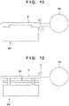
- a standing vortex may be formed in the gas flow. Such a standing vortex may blow up particles and adhere the particles to the substrate S. It was also confirmed by simulations that even if a substrate holding structure SH' configured to hold the substrate S includes a flat facing surface OS' parallel to the lower surface of the substrate S, a standing vortex is formed in the gas flow, as schematically indicated by a dotted arrow in Fig. 12 . Such a standing vortex may blow up particles and adhere the particles to the substrate S.
- the substrate holding structure 120 can include a first member 125 with the facing surface OS, and a second member 126 with an upper surface US facing a lower surface LS of the first member 125.
- the substrate holding structure 120 can include a plurality of contact portions 124 that contact the substrate S so as to support the substrate S.
- the second member 126 can support the first member 125 and the plurality of contact portions 124.
- the upper surface US of the second member 126 can have a shape along the lower surface LS of the first member 125. Such a structure enables the smooth flow of the gas.
- first member 125 lower surface LS
- second member 126 upper surface US
- a structure in which the space defined by the first member 125 (lower surface LS) and the second member 126 (upper surface US), which face each other does not exist as a channel for the gas, that is, with a structure in which the space is filled with a solid, the gas flow is impeded, and a standing vortex may be generated.
- a structure in which the first member 125 (lower surface LS) and the second member 126 (upper surface US) face each other is advantageous in suppressing generation of a standing vortex.
- the load lock device 100 can include a driving mechanism 130.
- the driving mechanism 130 can be arranged on the lower side of the load lock chamber 110 to move the substrate holding structure 120 up and down.
- the driving mechanism 130 can be connected to the substrate holding structure 120 via a connecting member 122.
- the load lock chamber 110 can include an extension chamber 140 extended from the lower portion of the load lock chamber 110 to a side, and a pump 150 arranged on the lower side of the extension chamber 140 and discharge a gas in the load lock chamber 110 via the extension chamber 140.
- the extension chamber 140 can include a bottom surface 144 with an opening 142 at a position deviated from the vertically lower position of the substrate holding structure 120.
- the pump 150 can be connected to the opening 142.
- a valve can be arranged between the pump 150 and the opening 142.
- the pump 150 can include, for example, a rotary pump, and a turbomolecular pump arranged between the rotary pump and the opening 142.
- the turbine of the turbomolecular pump rotates at a high speed during the operation. If particles sucked by the turbomolecular pump collide against the turbine, these may be bounced by the turbine.
- the pump 150 itself may generate particles independently of whether the pump 150 is a turbomolecular pump or not.
- the pump 150 is connected to the opening 142 provided in the bottom surface 144 of the extension chamber 140 extended from the lower portion of the load lock chamber 110 to the side. This can reduce the particles from the pump 150 reaching the space above the substrate S via a gap G between the side surface of the substrate holding structure 120 and the inner side surface of the load lock chamber and adhering to the substrate S.
- a gas discharge line 52 can be connected to the valve 50 arranged between the loader chamber 30 and the second conveyance port 112 of the load lock chamber 110.
- the gas in the space near the second conveyance port 112 can be discharged to the external space of the load lock chamber 110 via the gas discharge line 52.
- a pump (not shown) can be connected to the gas discharge line 52.
- At least a part of the second conveyance port 112 can be arranged above (vertically above) the extension chamber 140.
- at least a part of the extension chamber 140 can be arranged between the second conveyance port 112 and the pump 150. This configuration is advantageous in reducing the foot print of the load lock device 100.
- At least a part of the loader chamber 30 can be arranged above (vertically above) the extension chamber 140.
- at least a part of the extension chamber 140 can be arranged between the loader chamber 30 and the pump 150. This configuration is also advantageous in reducing the foot print of the load lock device 100.
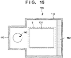
- Fig. 15 is a plan view showing the arrangement of the load lock chamber 110, the extension chamber 140, and the gas dispersing portion 162.
- This plan view can also be understood as an orthogonal projection to the floor on which the load lock device 100 is arranged.
- the substrate holder 120 can be located between the gas dispersing portion 162 and the extension chamber 140.
- the opening 142 can be located between the gas dispersing portion 162 and the extension chamber 140.
- the area of the gap G between the side surface of the substrate holding structure 120 and the inner side surface of the load lock chamber 110 is preferably smaller than the sectional area of the second conveyance port 112.
- the area of the gap G is more preferably smaller than 1/2, 1/3, or 1/4 of the sectional area of the second conveyance port 112.
- the area of the gap G between the side surface of the substrate holding structure 120 and the inner side surface of the load lock chamber 110 is preferably smaller than the sectional area of the opening 142 provided in the bottom surface 144 of the extension chamber 140. This configuration is advantageous in reducing the particles from the pump 150 reaching the space above the substrate S via the gap G and adhering to the substrate S.
- the area of the gap G is preferably smaller than the sectional area (the sectional area along a vertical plane) of a connection portion 146 between the load lock chamber 110 and the extension chamber 140. This configuration is also advantageous in reducing the particles from the pump 150 reaching the space above the substrate S via the gap G and adhering to the substrate S.
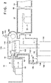
- Figs. 2 , 3 , 4 , and 5 exemplarily show the operation of the processing device shown in Fig. 1 .
- the gas in the internal space can be discharged by the pump 150 to the external space of the load lock chamber 110.
- the introduction amount of the gas from the gas introducing portion 160 to the internal space can be made larger than the gas discharge amount by the pump 150.
- the valve 50 can be opened, as shown in Fig. 2 , and the gas discharge via the gas discharge line 52 can be started.
- the conveyance robot 34 can convey the substrate S from the loader chamber 30 to the substrate holding structure 120 in the internal space of the load lock chamber 110.
- the valve 50 can be closed, and the substrate holding structure 120 can be driven upward by the driving mechanism 130. Also, in a state in which the gas is introduced from the gas introducing portion 160 to the internal space of the load lock chamber 110, the gas discharge amount from the internal space by the pump 150 is increased, and the pressure in the internal space is reduced. After that, gas introduction to the internal space by the gas introducing portion 160 can be stopped, and the gas discharge amount from the internal space by the pump 150 can further be increased.
- the substrate holding structure 120 can be driven downward by the driving mechanism 130 up to a height to convey the substrate S to the transfer chamber 20, as shown in Fig. 4 .
- the valve 40 can be opened, and the conveyance robot 22 can convey the substrate S from the internal space of the load lock chamber 110 to the transfer chamber 20 and then to the reduced-pressure processing device 10. Then, the valve 40 is closed, and the substrate S is processed in the reduced-pressure processing device 10.
- valve 40 can be opened, and the conveyance robot 22 can convey the substrate S in the reduced-pressure processing device 10 to the internal space of the load lock chamber 110, as shown in Fig. 5 . After that, the valve 40 can be closed.
- the gas in the internal space can be discharged by the pump 150 to the external space of the load lock chamber 110.
- the introduction amount of the gas from the gas introducing portion 160 to the internal space can be made larger than the gas discharge amount by the pump 150.
- the valve 50 can be opened, as shown in Fig. 2 , and the gas discharge via the gas discharge line 52 can be started.
- the conveyance robot 34 can convey the substrate S from the substrate holding structure 120 in the internal space of the load lock chamber 110 to the loader chamber 30.
- the valve 50 can be closed, and the gas discharge via the gas discharge line 52 can be stopped.
- the substrate holding structure 120 can hold the substrate S such that at least a part of the side surface (outer peripheral surface) of the substrate S faces the inner surface of the load lock chamber 110.
- the substrate holding structure 120 can hold the substrate S such that the at least part of the side surface (outer peripheral surface) of the substrate S held by the substrate holding structure 120 can face the inner surface of the load lock chamber 110 concerning a direction parallel to the surface of the substrate S.
- the substrate holding structure 120 can be arranged at a plurality of positions in the internal space of the load lock chamber 110.
- the plurality of positions can include a position where a part of the side surface of the substrate S held by the substrate holding structure 120 faces the gas dispersing portion 162, as shown in Fig. 1 .
- the part of the side surface (outer peripheral surface) of the substrate S held by the substrate holding structure 120 can face the gas dispersing portion 162 concerning a direction parallel to the surface of the substrate S.
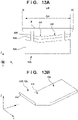
- the substrate holding structure 120 may be configured such that a size DH of the facing surface OS of the substrate holding structure 120 in a surface direction (a direction parallel to the X-Y plane) along the surface of the substrate S is smaller than a size DS of the substrate S in the surface direction.
- the portion PP of the substrate holding structure 120 can be located inside the outer edge EE of the facing surface OS concerning a predetermined direction (Y direction) in a horizontal plane (X-Y plane).
- the cross sections of the facing surface OS cut along a plurality of planes (a plurality of planes parallel to the Y-Z plane) that are perpendicular to the horizontal plane (X-Y plane) and parallel to the predetermined direction (Y direction) can have shapes identical to each other.
- the substrate S held by the substrate holding structure 120 can have a rectangular shape.
- the substrate S held by the substrate holding structure 120 can have a circular shape with a notch portion NT indicating a reference direction.
- the substrate S held by the substrate holding structure 120 may have another shape.
- Fig. 6 schematically shows the configuration of a processing device including a load lock device 100 according to the second embodiment of the present invention. Matters that are not mentioned as the second embodiment can comply with the first embodiment.
- the load lock device 100 according to the second embodiment includes a portion 601 where the ceiling portion of a load lock chamber 110 faces the inside region of the outer edge of a substrate S, and a portion 602 facing the outer edge of the substrate S, and the distance between the portion 601 and the substrate S is larger than the distance between the portion 602 and the substrate S.
- Fig. 7 schematically shows the configuration of a processing device including a load lock device 100 according to the third embodiment of the present invention. Matters that are not mentioned as the third embodiment can comply with the first embodiment.
- the load lock device 100 according to the third embodiment includes a portion 601 where the ceiling portion of a load lock chamber 110 faces the inside region of the outer edge of a substrate S, and a portion 602 facing the outer edge of the substrate S, and the distance between the portion 601 and the substrate S is larger than the distance between the portion 602 and the substrate S.
- the portion 601 is formed by a smooth curved surface.
- Fig. 8 schematically shows the configuration of a processing device including a load lock device 100 according to the fourth embodiment of the present invention. Matters that are not mentioned as the fourth embodiment can comply with the first embodiment.
- a first member 125 has a corrugated wing shape.
- the corrugated wing shape is advantageous in, for example, suppressing a large vortex throughout the space between a facing surface OS and a substrate S.
- Fig. 9 schematically shows a plan view of a first member 125 in a load lock device 100 according to the fifth embodiment of the present invention.
- Fig. 10 schematically shows a side view of the first member 125 in the load lock device 100 according to the fifth embodiment of the present invention. Matters that are not mentioned as the fifth embodiment can comply with the first embodiment.
- a portion PP located inside an outer edge EE of a facing surface OS is located inside the outer edge EE of the facing surface OS concerning a predetermined direction DIR
- the first member 125 is divided into a plurality of portions 125a and 125b concerning a direction orthogonal to the predetermined direction DIR.
- 100...load lock device 110...load lock chamber, 111...first conveyance port, 112...second conveyance port, 120...substrate holding structure, 140...extension chamber, 142...opening, 144...bottom surface, 150...pump, 160...gas introducing portion, 162...gas dispersing portion, PP...portion, EE...outer edge, OS...facing surface
Landscapes
- Container, Conveyance, Adherence, Positioning, Of Wafer (AREA)
- Drying Of Semiconductors (AREA)
- Mechanical Control Devices (AREA)
- Chairs Characterized By Structure (AREA)
- Jib Cranes (AREA)
- Glass Compositions (AREA)
- Amplifiers (AREA)
- Fats And Perfumes (AREA)
- Vehicle Body Suspensions (AREA)
- Push-Button Switches (AREA)
- Load-Engaging Elements For Cranes (AREA)
Abstract
Description
- The present invention relates to a load lock device.
- PTL 1 discloses a vacuum processing device including a load lock chamber, a wafer stage arranged in the load lock chamber, and a mechanism configured to move the wafer stage up and down. The wafer stage has a convex shape.
- In a substrate holding structure having a structure like the wafer stage described in PTL 1, the wafer stage may generate a standing vortex when forming a gas flow in the load lock chamber. Such a standing vortex may, for example, blow up particles from the lower side of a substrate to above the substrate and adhere the particles to the substrate.
- PTL 1:
Japanese Patent Laid-Open No. 5-140743 - The present invention provides a technique advantageous in preventing particles from adhering to a substrate.
- According to one aspect of the present invention, in a load lock device comprising a load lock chamber, and a substrate holding structure configured to hold a substrate in the load lock chamber, the substrate holding structure includes a facing surface facing the substrate, and is configured to allow a gas to flow through a space between the substrate and the facing surface, and in a state in which the substrate is held by the substrate holding structure, a distance between the substrate and a portion located inside an outer edge of the facing surface is larger than a distance between the substrate and the outer edge of the facing surface.
-
-
Fig. 1 is a view schematically showing the configuration of a processing device including a load lock device according to the first embodiment of the present invention; -
Fig. 2 is a view showing the operation of the processing device including the load lock device according to the first embodiment of the present invention; -
Fig. 3 is a view showing the operation of the processing device including the load lock device according to the first embodiment of the present invention; -
Fig. 4 is a view showing the operation of the processing device including the load lock device according to the first embodiment of the present invention; -
Fig. 5 is a view showing the operation of the processing device including the load lock device according to the first embodiment of the present invention; -
Fig. 6 is a view showing the operation of a processing device including a load lock device according to the second embodiment of the present invention; -
Fig. 7 is a view showing the operation of a processing device including a load lock device according to the third embodiment of the present invention; -
Fig. 8 is a view showing the operation of a processing device including a load lock device according to the fourth embodiment of the present invention; -
Fig. 9 is a schematic plan view of a first member in a load lock device according to the fifth embodiment of the present invention; -
Fig. 10 is an enlarged schematic side view of a substrate holding structure in each of the load lock devices according to the first and fifth embodiments of the present invention; -
Fig. 11 is a view for explaining a problem; -
Fig. 12 is a view for explaining a problem; -
Fig. 13A is a view showing a substrate holding structure; -
Fig. 13B is a view showing the shape of the first member or facing surface of the substrate holding structure shown inFig. 13A ; -
Fig. 14A is a view showing an example of a substrate; -
Fig. 14B is a view showing another example of the substrate; and -
Fig. 15 is a plan view showing the arrangement of a load lock chamber, an extension chamber, and a gas dispersing portion. - Hereinafter, embodiments will be described in detail with reference to the attached drawings. Note, the following embodiments are not intended to limit the scope of the claimed invention. Multiple features are described in the embodiments, but limitation is not made to an invention that requires all such features, and multiple such features may be combined as appropriate. Furthermore, in the attached drawings, the same reference numerals are given to the same or similar configurations, and redundant description thereof is omitted.
-
Fig. 1 schematically shows the configuration of a processing device including aload lock device 100 according to the first embodiment of the present invention. Theload lock device 100 can include aload lock chamber 110 arranged between aloader chamber 30 and atransfer chamber 20. Theloader chamber 30 can be maintained in an atmospheric environment. In theloader chamber 30, for example, a substrate S can be provided from a carrier. Alternatively, the substrate S can be provided from a pre-processing device to theloader chamber 30. Theloader chamber 30 can include afilter 32 on the ceiling, and a downflow can be supplied to the internal space of theloader chamber 30 via thefilter 32. Aconveyance robot 34 is arranged in theloader chamber 30, and the substrate S can be conveyed by theconveyance robot 34. Theconveyance robot 34 can convey the substrate S from theloader chamber 30 to theload lock chamber 110 via avalve 50. The pressure in theload lock chamber 110 to which the substrate S is conveyed is sufficiently reduced. After that, aconveyance robot 22 arranged in thetransfer chamber 20 can convey the substrate S from theload lock chamber 110 to thetransfer chamber 20 via avalve 40. After that, theconveyance robot 22 can convey the substrate S from thetransfer chamber 20 to a reduced-pressure processing device 10 via avalve 60. The reduced-pressure processing device 10 can be one of, for example, a CVD device, a PVD device, an etching device, a plasma processing device, and an electron-beam exposure device. - The
load lock chamber 110 can include afirst conveyance port 111 connected to thetransfer chamber 20 connected to the reduced-pressure processing device 10, and asecond conveyance port 112 connected to theloader chamber 30. In an example, the height of the first conveyance port 111 (for example, the height of the lower end of the first conveyance port 111) is lower than the height of the second conveyance port 112 (for example, the height of the lower end of the second conveyance port 112). Thefirst conveyance port 111 can be arranged to communicate with the internal space of thetransfer chamber 20 via thevalve 40. Thesecond conveyance port 112 can be arranged to communicate with the internal space of theloader chamber 30 via thevalve 50. - The
load lock device 100 can include agas introducing portion 160 that introduces a gas (for example, clean dry air or nitrogen gas) into theload lock chamber 110. Thegas introducing portion 160 can be arranged above a path between asubstrate holding structure 120 and thetransfer chamber 20 in a state in which, for example, the substrate S is conveyed to thetransfer chamber 20 via thefirst conveyance port 111. In an example, thegas introducing portion 160 can be arranged above thefirst conveyance port 111. Thegas introducing portion 160 can include agas dispersing portion 162 that disperses the gas to the internal space of theload lock chamber 110. At least a part of thegas dispersing portion 162 can be arranged in theload lock chamber 110. Thegas dispersing portion 162 can be arranged at a position facing thesecond conveyance port 112. Thegas introducing portion 160 can include aflow adjusting valve 164 that adjusts the gas introduction. Thegas dispersing portion 162 can have a pillar-shaped portion. The inner side surface of theload lock chamber 110 can be apart from the pillar-shaped portion, and can include a curved surface along the pillar-shaped portion. The pillar-shaped portion can have a columnar shape, and the curved surface can form a part of a cylindrical surface. - The
load lock device 100 can have thesubstrate holding structure 120 that holds the substrate S in theload lock chamber 110. Thesubstrate holding structure 120 can include a facing surface OS facing the substrate S, and can be configured to allow a gas to flow through a space between the substrate S and the facing surface OS. As shown in the enlarged view ofFig. 10 , thesubstrate holding structure 120 can have a structure in which the distance between the substrate S and a portion PP located inside an outer edge EE of the facing surface OS is larger than the distance between the substrate S and the outer edge EE of the facing surface OS in a state in which the substrate S is held by thesubstrate holding structure 120. It was confirmed by simulations that such a structure can effectively suppress formation of a standing vortex in a gas flow in the internal space of theload lock chamber 110, as schematically indicated by dotted arrows inFig. 10 . Here, the gas flow can be formed by introducing the gas to the internal space of theload lock chamber 110 by thegas introducing portion 160 and/or discharging the gas from the internal space by thepump 150 or the like as will be described later. Hence, the gas flow can necessarily be formed in theload lock chamber 110 in which the pressure changes in a wide range from the atmospheric pressure to a high vacuum. - On the other hand, as schematically indicated by dotted arrows in
Fig. 11 , if a substrate holding structure SH configured to hold the substrate S includes a wall that impedes the gas flow, a standing vortex may be formed in the gas flow. Such a standing vortex may blow up particles and adhere the particles to the substrate S. It was also confirmed by simulations that even if a substrate holding structure SH' configured to hold the substrate S includes a flat facing surface OS' parallel to the lower surface of the substrate S, a standing vortex is formed in the gas flow, as schematically indicated by a dotted arrow inFig. 12 . Such a standing vortex may blow up particles and adhere the particles to the substrate S. - Referring back to
Fig. 1 , thesubstrate holding structure 120 can include afirst member 125 with the facing surface OS, and asecond member 126 with an upper surface US facing a lower surface LS of thefirst member 125. Thesubstrate holding structure 120 can include a plurality ofcontact portions 124 that contact the substrate S so as to support the substrate S. Thesecond member 126 can support thefirst member 125 and the plurality ofcontact portions 124. The upper surface US of thesecond member 126 can have a shape along the lower surface LS of thefirst member 125. Such a structure enables the smooth flow of the gas. With a structure in which the space defined by the first member 125 (lower surface LS) and the second member 126 (upper surface US), which face each other, does not exist as a channel for the gas, that is, with a structure in which the space is filled with a solid, the gas flow is impeded, and a standing vortex may be generated. On the other hand, a structure in which the first member 125 (lower surface LS) and the second member 126 (upper surface US) face each other is advantageous in suppressing generation of a standing vortex. - The
load lock device 100 can include adriving mechanism 130. Thedriving mechanism 130 can be arranged on the lower side of theload lock chamber 110 to move thesubstrate holding structure 120 up and down. Thedriving mechanism 130 can be connected to thesubstrate holding structure 120 via a connectingmember 122. - The
load lock chamber 110 can include anextension chamber 140 extended from the lower portion of theload lock chamber 110 to a side, and apump 150 arranged on the lower side of theextension chamber 140 and discharge a gas in theload lock chamber 110 via theextension chamber 140. Theextension chamber 140 can include abottom surface 144 with anopening 142 at a position deviated from the vertically lower position of thesubstrate holding structure 120. Thepump 150 can be connected to theopening 142. Although not illustrated, a valve can be arranged between thepump 150 and theopening 142. - The
pump 150 can include, for example, a rotary pump, and a turbomolecular pump arranged between the rotary pump and theopening 142. The turbine of the turbomolecular pump rotates at a high speed during the operation. If particles sucked by the turbomolecular pump collide against the turbine, these may be bounced by the turbine. In addition, thepump 150 itself may generate particles independently of whether thepump 150 is a turbomolecular pump or not. Hence, it is preferable that thepump 150 is connected to theopening 142 provided in thebottom surface 144 of theextension chamber 140 extended from the lower portion of theload lock chamber 110 to the side. This can reduce the particles from thepump 150 reaching the space above the substrate S via a gap G between the side surface of thesubstrate holding structure 120 and the inner side surface of the load lock chamber and adhering to the substrate S. - A
gas discharge line 52 can be connected to thevalve 50 arranged between theloader chamber 30 and thesecond conveyance port 112 of theload lock chamber 110. The gas in the space near thesecond conveyance port 112 can be discharged to the external space of theload lock chamber 110 via thegas discharge line 52. A pump (not shown) can be connected to thegas discharge line 52. - At least a part of the
second conveyance port 112 can be arranged above (vertically above) theextension chamber 140. Alternatively, at least a part of theextension chamber 140 can be arranged between thesecond conveyance port 112 and thepump 150. This configuration is advantageous in reducing the foot print of theload lock device 100. - At least a part of the
loader chamber 30 can be arranged above (vertically above) theextension chamber 140. Alternatively, at least a part of theextension chamber 140 can be arranged between theloader chamber 30 and thepump 150. This configuration is also advantageous in reducing the foot print of theload lock device 100. -
Fig. 15 is a plan view showing the arrangement of theload lock chamber 110, theextension chamber 140, and thegas dispersing portion 162. This plan view can also be understood as an orthogonal projection to the floor on which theload lock device 100 is arranged. In the plan view or orthogonal projection, thesubstrate holder 120 can be located between thegas dispersing portion 162 and theextension chamber 140. Alternatively, in the plan view or orthogonal projection, theopening 142 can be located between thegas dispersing portion 162 and theextension chamber 140. - The area of the gap G between the side surface of the
substrate holding structure 120 and the inner side surface of theload lock chamber 110 is preferably smaller than the sectional area of thesecond conveyance port 112. The area of the gap G is more preferably smaller than 1/2, 1/3, or 1/4 of the sectional area of thesecond conveyance port 112. When the substrate S is conveyed from theloader chamber 30 to the internal space of theload lock chamber 110 via thesecond conveyance port 112, this configuration is advantageous in increasing the amount of the gas introduced from thegas dispersing portion 162 to the internal space of theload lock chamber 110 and discharged via thesecond conveyance port 112 and thegas discharge line 52 as compared to the amount of the gas discharged from the space above the substrate S to the space below thesubstrate holding structure 120 via the gap G. This is effective to suppress particles entering from theloader chamber 30 to the internal space of theload lock chamber 110 via thesecond conveyance port 112. - The area of the gap G between the side surface of the
substrate holding structure 120 and the inner side surface of theload lock chamber 110 is preferably smaller than the sectional area of theopening 142 provided in thebottom surface 144 of theextension chamber 140. This configuration is advantageous in reducing the particles from thepump 150 reaching the space above the substrate S via the gap G and adhering to the substrate S. The area of the gap G is preferably smaller than the sectional area (the sectional area along a vertical plane) of aconnection portion 146 between theload lock chamber 110 and theextension chamber 140. This configuration is also advantageous in reducing the particles from thepump 150 reaching the space above the substrate S via the gap G and adhering to the substrate S. -
Figs. 2 ,3 ,4 , and5 exemplarily show the operation of the processing device shown inFig. 1 . First, while introducing (supplying) the gas from thegas introducing portion 160 to the internal space of theload lock chamber 110, the gas in the internal space can be discharged by thepump 150 to the external space of theload lock chamber 110. At this time, to raise the pressure in the internal space, the introduction amount of the gas from thegas introducing portion 160 to the internal space can be made larger than the gas discharge amount by thepump 150. When the pressure in the internal space becomes equal to or more than the atmospheric pressure, thevalve 50 can be opened, as shown inFig. 2 , and the gas discharge via thegas discharge line 52 can be started. After that, theconveyance robot 34 can convey the substrate S from theloader chamber 30 to thesubstrate holding structure 120 in the internal space of theload lock chamber 110. - After that, as shown in
Fig. 3 , thevalve 50 can be closed, and thesubstrate holding structure 120 can be driven upward by thedriving mechanism 130. Also, in a state in which the gas is introduced from thegas introducing portion 160 to the internal space of theload lock chamber 110, the gas discharge amount from the internal space by thepump 150 is increased, and the pressure in the internal space is reduced. After that, gas introduction to the internal space by thegas introducing portion 160 can be stopped, and the gas discharge amount from the internal space by thepump 150 can further be increased. - When the pressure in the internal space of the
load lock chamber 110 is sufficiently reduced, thesubstrate holding structure 120 can be driven downward by thedriving mechanism 130 up to a height to convey the substrate S to thetransfer chamber 20, as shown inFig. 4 . After that, as shown inFig. 5 , thevalve 40 can be opened, and theconveyance robot 22 can convey the substrate S from the internal space of theload lock chamber 110 to thetransfer chamber 20 and then to the reduced-pressure processing device 10. Then, thevalve 40 is closed, and the substrate S is processed in the reduced-pressure processing device 10. - After that, the
valve 40 can be opened, and theconveyance robot 22 can convey the substrate S in the reduced-pressure processing device 10 to the internal space of theload lock chamber 110, as shown inFig. 5 . After that, thevalve 40 can be closed. - Then, while introducing the gas from the
gas introducing portion 160 to the internal space of theload lock chamber 110, the gas in the internal space can be discharged by thepump 150 to the external space of theload lock chamber 110. At this time, to raise the pressure in the internal space, the introduction amount of the gas from thegas introducing portion 160 to the internal space can be made larger than the gas discharge amount by thepump 150. When the pressure in the internal space becomes equal to or more than the atmospheric pressure, thevalve 50 can be opened, as shown inFig. 2 , and the gas discharge via thegas discharge line 52 can be started. After that, theconveyance robot 34 can convey the substrate S from thesubstrate holding structure 120 in the internal space of theload lock chamber 110 to theloader chamber 30. After that, thevalve 50 can be closed, and the gas discharge via thegas discharge line 52 can be stopped. - As shown in
Figs. 1 ,3 , and4 , thesubstrate holding structure 120 can hold the substrate S such that at least a part of the side surface (outer peripheral surface) of the substrate S faces the inner surface of theload lock chamber 110. Here, thesubstrate holding structure 120 can hold the substrate S such that the at least part of the side surface (outer peripheral surface) of the substrate S held by thesubstrate holding structure 120 can face the inner surface of theload lock chamber 110 concerning a direction parallel to the surface of the substrate S. - As shown in
Figs. 1 to 5 , thesubstrate holding structure 120 can be arranged at a plurality of positions in the internal space of theload lock chamber 110. The plurality of positions can include a position where a part of the side surface of the substrate S held by thesubstrate holding structure 120 faces thegas dispersing portion 162, as shown inFig. 1 . Here, the part of the side surface (outer peripheral surface) of the substrate S held by thesubstrate holding structure 120 can face thegas dispersing portion 162 concerning a direction parallel to the surface of the substrate S. - As shown in
Fig. 13A , thesubstrate holding structure 120 may be configured such that a size DH of the facing surface OS of thesubstrate holding structure 120 in a surface direction (a direction parallel to the X-Y plane) along the surface of the substrate S is smaller than a size DS of the substrate S in the surface direction. As shown inFigs. 13A and 13B , the portion PP of thesubstrate holding structure 120 can be located inside the outer edge EE of the facing surface OS concerning a predetermined direction (Y direction) in a horizontal plane (X-Y plane). The cross sections of the facing surface OS cut along a plurality of planes (a plurality of planes parallel to the Y-Z plane) that are perpendicular to the horizontal plane (X-Y plane) and parallel to the predetermined direction (Y direction) can have shapes identical to each other. - As shown in
Fig. 14A , the substrate S held by thesubstrate holding structure 120 can have a rectangular shape. Alternatively, as shown inFig. 14B , the substrate S held by thesubstrate holding structure 120 can have a circular shape with a notch portion NT indicating a reference direction. However, the substrate S held by thesubstrate holding structure 120 may have another shape. -
Fig. 6 schematically shows the configuration of a processing device including aload lock device 100 according to the second embodiment of the present invention. Matters that are not mentioned as the second embodiment can comply with the first embodiment. Theload lock device 100 according to the second embodiment includes aportion 601 where the ceiling portion of aload lock chamber 110 faces the inside region of the outer edge of a substrate S, and aportion 602 facing the outer edge of the substrate S, and the distance between theportion 601 and the substrate S is larger than the distance between theportion 602 and the substrate S. -
Fig. 7 schematically shows the configuration of a processing device including aload lock device 100 according to the third embodiment of the present invention. Matters that are not mentioned as the third embodiment can comply with the first embodiment. Theload lock device 100 according to the third embodiment includes aportion 601 where the ceiling portion of aload lock chamber 110 faces the inside region of the outer edge of a substrate S, and aportion 602 facing the outer edge of the substrate S, and the distance between theportion 601 and the substrate S is larger than the distance between theportion 602 and the substrate S. In the third embodiment, theportion 601 is formed by a smooth curved surface. -
Fig. 8 schematically shows the configuration of a processing device including aload lock device 100 according to the fourth embodiment of the present invention. Matters that are not mentioned as the fourth embodiment can comply with the first embodiment. In the fourth embodiment, afirst member 125 has a corrugated wing shape. The corrugated wing shape is advantageous in, for example, suppressing a large vortex throughout the space between a facing surface OS and a substrate S. -
Fig. 9 schematically shows a plan view of afirst member 125 in aload lock device 100 according to the fifth embodiment of the present invention.Fig. 10 schematically shows a side view of thefirst member 125 in theload lock device 100 according to the fifth embodiment of the present invention. Matters that are not mentioned as the fifth embodiment can comply with the first embodiment. In the fifth embodiment, in a state in which a substrate S is held by asubstrate holding structure 120, a portion PP located inside an outer edge EE of a facing surface OS is located inside the outer edge EE of the facing surface OS concerning a predetermined direction DIR, and thefirst member 125 is divided into a plurality ofportions - The present invention is not limited to the above embodiments and various changes and modifications can be made within the spirit and scope of the present invention. Therefore, to apprise the public of the scope of the present invention, the following claims are made.
- 100...load lock device, 110...load lock chamber, 111...first conveyance port, 112...second conveyance port, 120...substrate holding structure, 140...extension chamber, 142...opening, 144...bottom surface, 150...pump, 160...gas introducing portion, 162...gas dispersing portion, PP...portion, EE...outer edge, OS...facing surface
Claims (19)
- A load lock device comprising a load lock chamber, and a substrate holding structure configured to hold a substrate in the load lock chamber, characterized in thatthe substrate holding structure includes a facing surface facing the substrate, and is configured to allow a gas to flow through a space between the substrate and the facing surface, andin a state in which the substrate is held by the substrate holding structure, a distance between the substrate and a portion located inside an outer edge of the facing surface is larger than a distance between the substrate and the outer edge of the facing surface.
- The load lock device according to claim 1, characterized in that the substrate holding structure includes a first member with the facing surface, and a second member with an upper surface facing a lower surface of the first member.
- The load lock device according to claim 2, characterized in that the substrate holding structure further includes a plurality of contact portions configured to contact the substrate so as to support the substrate, and the second member supports the first member and the plurality of contact portions.
- The load lock device according to claim 3, characterized in that the upper surface of the second member has a shape along the lower surface of the first member.
- The load lock device according to claim 3, characterized in that the first member has a corrugated wing shape.
- The load lock device according to claim 3, characterized in thatthe portion is located inside the outer edge of the facing surface concerning a predetermined direction, andthe first member is divided into a plurality of portions concerning a direction orthogonal to the predetermined direction.
- The load lock device according to any one of claims 1 to 6, characterized in thatthe load lock chamber includes a first conveyance port connected to a transfer chamber connected to a reduced-pressure processing device, and a second conveyance port connected to a loader chamber, andthe load lock device further comprises:a gas introducing portion arranged above a path between the substrate holding structure and the transfer chamber in a state in which the substrate is conveyed to the transfer chamber via the first conveyance port; anda gas discharge portion arranged to discharge the gas via a space below the substrate holding structure.
- The load lock device according to claim 7, characterized in that a height of the first conveyance port is lower than a height of the second conveyance port.
- The load lock device according to claim 7 or 8, characterized in thatthe gas introducing portion includes a gas dispersing portion configured to disperse the gas, andthe gas dispersing portion is arranged at a position facing the second conveyance port.
- The load lock device according to claim 9, characterized in that
the gas dispersing portion has a pillar-shaped portion, and an inner side surface of the load lock chamber is apart from the pillar-shaped portion, and includes a curved surface along the pillar-shaped portion. - The load lock device according to claim 10, characterized in that the pillar-shaped portion has a columnar shape, and the curved surface forms a part of a cylindrical surface.
- The load lock device according to any one of claims 9 to 11, characterized in that the gas introducing portion and the gas discharge portion are controlled to execute an operation of lowering a pressure in the load lock chamber in a state in which the substrate held by the substrate holding structure is arranged at a position higher than a center axis of the gas dispersing portion, and an operation of lowering the pressure in the load lock chamber in a state in which the substrate held by the substrate holding structure is arranged at a position lower than the center axis of the gas dispersing portion.
- The load lock device according to any one of claims 7 to 12, characterized by further comprising a gas discharge line arranged to discharge the gas from a space near the second conveyance port.
- The load lock device according to any one of claims 1 to 13, characterized in that the substrate holding structure holds the substrate such that at least a part of a side surface of the substrate faces the inner surface of the load lock chamber.
- The load lock device according to any one of claims 1 to 8 and 13, characterized by further comprising a gas dispersing portion configured to disperse the gas in an internal space of the load lock chamber,wherein the substrate holding structure holds the substrate such that at least a part of a side surface of the substrate faces an inner surface of the load lock chamber, anda position where the substrate holding structure can be arranged includes a position where a part of the side surface of the substrate held by the substrate holding structure faces the gas dispersing portion.
- The load lock device according to any one of claims 1 to 15, characterized in that a size of the facing surface in a surface direction along a surface of the substrate is smaller than a size of the substrate in the surface direction.
- The load lock device according to any one of claims 1 to 16, characterized in thatthe portion is located inside the outer edge of the facing surface concerning a predetermined direction in a horizontal plane, andcross sections of the facing surface cut along a plurality of planes that are perpendicular to the horizontal plane and parallel to the predetermined direction have shapes identical to each other.
- The load lock device according to any one of claims 1 to 17, characterized in that the substrate held by the substrate holding structure has a rectangular shape.
- The load lock device according to any one of claims 1 to 17, characterized in that the substrate held by the substrate holding structure has a circular shape with a notch portion indicating a reference direction.
Applications Claiming Priority (2)
| Application Number | Priority Date | Filing Date | Title |
|---|---|---|---|
| PCT/JP2019/035248 WO2021044623A1 (en) | 2019-09-06 | 2019-09-06 | Load lock device |
| PCT/JP2020/033161 WO2021045070A1 (en) | 2019-09-06 | 2020-09-02 | Load lock device |
Publications (2)
| Publication Number | Publication Date |
|---|---|
| EP4027371A1 true EP4027371A1 (en) | 2022-07-13 |
| EP4027371A4 EP4027371A4 (en) | 2023-10-04 |
Family
ID=74200175
Family Applications (1)
| Application Number | Title | Priority Date | Filing Date |
|---|---|---|---|
| EP20861168.1A Pending EP4027371A4 (en) | 2019-09-06 | 2020-09-02 | LOAD LOCKING DEVICE |
Country Status (7)
| Country | Link |
|---|---|
| US (2) | US12211735B2 (en) |
| EP (1) | EP4027371A4 (en) |
| JP (3) | JP6818930B1 (en) |
| KR (2) | KR102823924B1 (en) |
| CN (2) | CN114175225B (en) |
| TW (2) | TWI776224B (en) |
| WO (2) | WO2021044623A1 (en) |
Families Citing this family (1)
| Publication number | Priority date | Publication date | Assignee | Title |
|---|---|---|---|---|
| WO2021044622A1 (en) * | 2019-09-06 | 2021-03-11 | キヤノンアネルバ株式会社 | Load lock device |
Family Cites Families (23)
| Publication number | Priority date | Publication date | Assignee | Title |
|---|---|---|---|---|
| JP3276382B2 (en) | 1991-11-21 | 2002-04-22 | 東京エレクトロン株式会社 | Vacuum processing device and vacuum processing method |
| JP2939378B2 (en) * | 1991-11-21 | 1999-08-25 | 東京エレクトロン株式会社 | Vacuum processing equipment |
| US5223001A (en) | 1991-11-21 | 1993-06-29 | Tokyo Electron Kabushiki Kaisha | Vacuum processing apparatus |
| JP2000126581A (en) * | 1998-10-29 | 2000-05-09 | Kokusai Electric Co Ltd | Load lock device |
| JP3570930B2 (en) * | 1999-09-02 | 2004-09-29 | 日本エー・エス・エム株式会社 | Gas introduction device to load lock chamber |
| JP4118189B2 (en) * | 2003-05-20 | 2008-07-16 | 株式会社日立ハイテクノロジーズ | Load lock device |
| JP2005140743A (en) | 2003-11-10 | 2005-06-02 | Nippon Sheet Glass Co Ltd | Performance evaluation method for processing means, and processing performance evaluation system using the same |
| JP2006093543A (en) * | 2004-09-27 | 2006-04-06 | Tokyo Electron Ltd | Heat treatment equipment |
| US20100270004A1 (en) * | 2005-05-12 | 2010-10-28 | Landess James D | Tailored profile pedestal for thermo-elastically stable cooling or heating of substrates |
| JP4616873B2 (en) * | 2007-09-28 | 2011-01-19 | 東京エレクトロン株式会社 | Semiconductor manufacturing apparatus, substrate holding method, and program |
| JP5291965B2 (en) * | 2008-03-25 | 2013-09-18 | 大日本スクリーン製造株式会社 | Heat treatment equipment |
| US8033771B1 (en) * | 2008-12-11 | 2011-10-11 | Novellus Systems, Inc. | Minimum contact area wafer clamping with gas flow for rapid wafer cooling |
| JP2010165841A (en) * | 2009-01-15 | 2010-07-29 | Tokyo Electron Ltd | Substrate cooling stage, and device for manufacturing semiconductor |
| TWI429873B (en) * | 2010-06-30 | 2014-03-11 | 愛發科股份有限公司 | Substrate processing apparatus and substrate cooling method |
| WO2012077547A1 (en) * | 2010-12-09 | 2012-06-14 | 東京エレクトロン株式会社 | Load lock device |
| KR20170102020A (en) * | 2015-01-23 | 2017-09-06 | 어플라이드 머티어리얼스, 인코포레이티드 | New susceptor design for removing deposited valleys in wafers |
| US10490437B2 (en) * | 2015-04-07 | 2019-11-26 | Sumco Corporation | Susceptor, vapor deposition apparatus, vapor deposition method and epitaxial silicon wafer |
| US9831110B2 (en) * | 2015-07-30 | 2017-11-28 | Lam Research Corporation | Vision-based wafer notch position measurement |
| JP6598242B2 (en) * | 2015-08-19 | 2019-10-30 | 芝浦メカトロニクス株式会社 | Substrate processing apparatus and substrate processing method |
| KR102615853B1 (en) * | 2015-10-15 | 2023-12-21 | 어플라이드 머티어리얼스, 인코포레이티드 | substrate carrier system |
| JP6270952B1 (en) * | 2016-09-28 | 2018-01-31 | 株式会社日立国際電気 | Substrate processing apparatus, semiconductor device manufacturing method, and recording medium. |
| KR102135409B1 (en) * | 2016-11-09 | 2020-07-17 | 주식회사 원익아이피에스 | Loadlock chamber and substrate processing apparatus having the same |
| US10302976B2 (en) * | 2017-05-09 | 2019-05-28 | Shenzhen China Star Optoelectronics Semiconductor Display Technology Co., Ltd. | Method and device for releasing film layer stress of array substrate |
-
2019
- 2019-09-06 WO PCT/JP2019/035248 patent/WO2021044623A1/en not_active Ceased
-
2020
- 2020-09-01 JP JP2020146982A patent/JP6818930B1/en active Active
- 2020-09-02 EP EP20861168.1A patent/EP4027371A4/en active Pending
- 2020-09-02 KR KR1020247030712A patent/KR102823924B1/en active Active
- 2020-09-02 CN CN202080051124.6A patent/CN114175225B/en active Active
- 2020-09-02 KR KR1020227003149A patent/KR102707828B1/en active Active
- 2020-09-02 WO PCT/JP2020/033161 patent/WO2021045070A1/en not_active Ceased
- 2020-09-02 CN CN202510933487.7A patent/CN120809638A/en active Pending
- 2020-09-04 TW TW109130338A patent/TWI776224B/en active
- 2020-09-04 TW TW111128248A patent/TWI819723B/en active
- 2020-09-15 JP JP2020154842A patent/JP6842804B1/en active Active
-
2021
- 2021-02-17 JP JP2021023675A patent/JP7473493B2/en active Active
-
2022
- 2022-01-14 US US17/575,690 patent/US12211735B2/en active Active
-
2024
- 2024-12-04 US US18/968,176 patent/US20260123351A1/en active Pending
Also Published As
| Publication number | Publication date |
|---|---|
| KR20240141851A (en) | 2024-09-27 |
| JP2021044545A (en) | 2021-03-18 |
| TW202117899A (en) | 2021-05-01 |
| CN114175225A (en) | 2022-03-11 |
| JP6842804B1 (en) | 2021-03-17 |
| TWI776224B (en) | 2022-09-01 |
| WO2021044623A1 (en) | 2021-03-11 |
| JP2021082834A (en) | 2021-05-27 |
| JP2021044551A (en) | 2021-03-18 |
| KR20220025880A (en) | 2022-03-03 |
| WO2021045070A1 (en) | 2021-03-11 |
| JP7473493B2 (en) | 2024-04-23 |
| US12211735B2 (en) | 2025-01-28 |
| US20260123351A1 (en) | 2026-04-30 |
| KR102823924B1 (en) | 2025-06-24 |
| CN120809638A (en) | 2025-10-17 |
| KR102707828B1 (en) | 2024-09-23 |
| US20220139761A1 (en) | 2022-05-05 |
| TWI819723B (en) | 2023-10-21 |
| JP6818930B1 (en) | 2021-01-27 |
| CN114175225B (en) | 2025-07-15 |
| TW202249155A (en) | 2022-12-16 |
| EP4027371A4 (en) | 2023-10-04 |
Similar Documents
| Publication | Publication Date | Title |
|---|---|---|
| JP2021141136A (en) | Substrate transfer system and atmospheric air transfer module | |
| US20260123351A1 (en) | Load lock device | |
| US8029227B2 (en) | Dust resistant load port apparatus and mini-environment system | |
| EP4027372A1 (en) | Load lock device | |
| CN113394143A (en) | Substrate conveying system, vacuum substrate conveying module and substrate conveying method | |
| CN110323171A (en) | Substrate suction means and semiconductor processing equipment | |
| CN116508141A (en) | Equipment and systems for delivering gases to process chambers | |
| KR20260038850A (en) | Vacuum processing apparatus and platen chamber | |
| CN113113326A (en) | Semiconductor processing machine | |
| TWM417646U (en) | A wafer container with at least one supporting module having a long slot |
Legal Events
| Date | Code | Title | Description |
|---|---|---|---|
| STAA | Information on the status of an ep patent application or granted ep patent |
Free format text: STATUS: THE INTERNATIONAL PUBLICATION HAS BEEN MADE |
|
| PUAI | Public reference made under article 153(3) epc to a published international application that has entered the european phase |
Free format text: ORIGINAL CODE: 0009012 |
|
| STAA | Information on the status of an ep patent application or granted ep patent |
Free format text: STATUS: REQUEST FOR EXAMINATION WAS MADE |
|
| 17P | Request for examination filed |
Effective date: 20220127 |
|
| AK | Designated contracting states |
Kind code of ref document: A1 Designated state(s): AL AT BE BG CH CY CZ DE DK EE ES FI FR GB GR HR HU IE IS IT LI LT LU LV MC MK MT NL NO PL PT RO RS SE SI SK SM TR |
|
| DAV | Request for validation of the european patent (deleted) | ||
| DAX | Request for extension of the european patent (deleted) | ||
| A4 | Supplementary search report drawn up and despatched |
Effective date: 20230906 |
|
| RIC1 | Information provided on ipc code assigned before grant |
Ipc: H01L 21/31 20060101ALI20230831BHEP Ipc: H01L 21/677 20060101ALI20230831BHEP Ipc: H01L 21/67 20060101ALI20230831BHEP Ipc: H01L 21/687 20060101ALI20230831BHEP Ipc: H01L 21/3065 20060101ALI20230831BHEP Ipc: H01L 21/02 20060101AFI20230831BHEP |
|
| REG | Reference to a national code |
Ref country code: DE Ref legal event code: R079 Free format text: PREVIOUS MAIN CLASS: H01L0021020000 Ipc: H10P0072000000 |
|
| GRAP | Despatch of communication of intention to grant a patent |
Free format text: ORIGINAL CODE: EPIDOSNIGR1 |
|
| STAA | Information on the status of an ep patent application or granted ep patent |
Free format text: STATUS: GRANT OF PATENT IS INTENDED |
|
| RIC1 | Information provided on ipc code assigned before grant |
Ipc: H10P 72/00 20260101AFI20260323BHEP Ipc: H10P 72/30 20260101ALI20260323BHEP Ipc: H10P 72/76 20260101ALI20260323BHEP Ipc: H10P 14/60 20260101ALI20260323BHEP Ipc: H10P 50/24 20260101ALI20260323BHEP Ipc: H10P 95/00 20260101ALI20260323BHEP |