EP4025017A1 - Member for controlling electromagnetic field - Google Patents
Member for controlling electromagnetic field Download PDFInfo
- Publication number
- EP4025017A1 EP4025017A1 EP20859030.7A EP20859030A EP4025017A1 EP 4025017 A1 EP4025017 A1 EP 4025017A1 EP 20859030 A EP20859030 A EP 20859030A EP 4025017 A1 EP4025017 A1 EP 4025017A1
- Authority
- EP
- European Patent Office
- Prior art keywords
- insulating member
- electromagnetic field
- field control
- hole
- control member
- Prior art date
- Legal status (The legal status is an assumption and is not a legal conclusion. Google has not performed a legal analysis and makes no representation as to the accuracy of the status listed.)
- Granted
Links
Images


Classifications
-
- H—ELECTRICITY
- H05—ELECTRIC TECHNIQUES NOT OTHERWISE PROVIDED FOR
- H05H—PLASMA TECHNIQUE; PRODUCTION OF ACCELERATED ELECTRICALLY-CHARGED PARTICLES OR OF NEUTRONS; PRODUCTION OR ACCELERATION OF NEUTRAL MOLECULAR OR ATOMIC BEAMS
- H05H7/00—Details of devices of the types covered by groups H05H9/00, H05H11/00, H05H13/00
- H05H7/04—Magnet systems, e.g. undulators, wigglers; Energisation thereof
-
- G—PHYSICS
- G21—NUCLEAR PHYSICS; NUCLEAR ENGINEERING
- G21K—HANDLING OF PARTICLES OR IONISING RADIATION NOT OTHERWISE PROVIDED FOR; IRRADIATION DEVICES; GAMMA RAY OR X-RAY MICROSCOPES
- G21K1/00—Arrangements for handling particles or ionising radiation, e.g. focusing or moderating
- G21K1/08—Deviation, concentration or focusing of the beam by electric or magnetic means
- G21K1/093—Deviation, concentration or focusing of the beam by electric or magnetic means by magnetic means
-
- H—ELECTRICITY
- H05—ELECTRIC TECHNIQUES NOT OTHERWISE PROVIDED FOR
- H05H—PLASMA TECHNIQUE; PRODUCTION OF ACCELERATED ELECTRICALLY-CHARGED PARTICLES OR OF NEUTRONS; PRODUCTION OR ACCELERATION OF NEUTRAL MOLECULAR OR ATOMIC BEAMS
- H05H7/00—Details of devices of the types covered by groups H05H9/00, H05H11/00, H05H13/00
- H05H7/04—Magnet systems, e.g. undulators, wigglers; Energisation thereof
- H05H2007/046—Magnet systems, e.g. undulators, wigglers; Energisation thereof for beam deflection
Definitions
- the present disclosure relates to an electromagnetic field control member, the member being used in accelerators or the like for accelerating charged particles such as electrons and heavy particles.
- CCiPM includes an insulating member having a cylindrical shape, the insulating member being made of a ceramic; a through hole formed along an axial direction of the insulating member, the through hole extending through a thickness direction of the insulating member; and a coil having a substrate shape, the coil being embedded in the through hole.
- the coil serves as a part of a partition wall that separates the inside and outside of the insulating member, and ensures airtightness inside the insulating member.
- Non Patent Document 1 Chikari Mitsuda et al., "Beam performance test of Ceramics Chamber with integrated Pulsed Magnet in beam transport-dump line for KEK PF-ring "
- An electromagnetic field control member includes a first insulating member made of a ceramic having a tubular shape, the first insulating member having a plurality of through holes extending in an axial direction; a conductive member made of a metal, the conductive member sealing off each of the through holes and leaving an opening portion in the through hole, the opening portion opening to an outer periphery of the first insulating member; a power feed terminal connected to the conductive member; and flanges respectively located at two ends of the first insulating member.
- a second insulating member made of a ceramic having a tubular shape is disposed on an outer peripheral side of the first insulating member, and includes two ends that are hermetically fixed to the flanges, respectively.
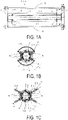
- FIG. 1A illustrates an electromagnetic field control member 100 according to an embodiment of the present disclosure, which is a CCiPM.
- the electromagnetic field control member 100 illustrated in FIG. 1 includes an insulating member 1, and flanges 2, 2 respectively located at two ends of the insulating member.
- the insulating member 1 includes a first insulating member 11 made of a ceramic having a tubular shape; and a second insulating member 12 made of a ceramic having a tubular shape disposed on an outer peripheral side of the first insulating member 11.
- a space 14 surrounded by an inner peripheral surface of the first insulating member 11 is formed inside the insulating member 1.
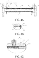
- the second insulating member 12 is positioned by mounting a sleeve 9 described below (see FIGS. 4B and 4C ).
- the first insulating member 11 includes a plurality of through holes 3 extending in an axial direction.
- axial direction refers to a direction along a center axis of the insulating member 1 made of the ceramic having the tubular shape.
- the second insulating member 12 includes through holes 31 that communicate with the through holes 3 of the first insulating member 11.
- the insulating member 1 includes a plurality of first power feed terminals 5 and a plurality of second power feed terminals 6 on two end surfaces thereof, respectively. As illustrated in FIG. IB, the first power feed terminals 5, 5 adjacent to each other are connected by a line 16 to form a magnetic field. Connection members 23 for feeding power are respectively connected to the second power feed terminals 6.
- a conductive member 4 is disposed in each of the through holes 3.
- the conductive member 4 is made of a metal, extends in the axial direction together with the through hole 3, and, as illustrated in FIGS. 2 and 3 , seals off the through hole 3 to form an opening portion 13 that opens to an outer periphery of the first insulating member 11.
- the conductive member 4 sealing off the through hole 3 ensures the airtightness of the space 14 surrounded by the inner peripheral surface of the first insulating member 11 (see FIGS. 1B, 1C , and 4A ).
- two end surfaces of the conductive member 4 in the axial direction are preferably curved surfaces that extend in the axial direction in a plan view.
- thermal stress remaining near both end surfaces of the conductive member 4 in the axial direction can be reduced even when heating and cooling are repeated.
- the width between inner walls of the through hole 3 may increase gradually, as in a tapered surface, from the inner peripheral side toward an outer peripheral side of the first insulating member 11.
- stress remaining in the first insulating member 11 is alleviated even when heating and cooling are repeated, and thus cracking in the first insulating member 11 can be suppressed over an extended period of time.
- an angle ⁇ 1 (see FIG. 3 ) formed by the inner walls opposed to each other may be 12° or more and 20° or less.
- the angle ⁇ 1 is within this range, the mechanical strength of the insulating member 1 can be maintained, and cracking in the insulating member 1 can be further suppressed.
- the angle ⁇ 1 formed by the inner walls opposed to each other may be measured in a cross section orthogonal to the axial direction.
- At least one of both end surfaces forming the through hole 4 may be inclined toward one of both ends in the axial direction in the cross-sectional view illustrated in FIG. 4C .
- An angle ⁇ 2 between a normal line n of a central axis and the end surface is, for example, 4° or more and 12° or less.
- the width between inner walls of the through hole 31 of the second insulating member 12 is substantially constant from an inner peripheral side toward an outer peripheral side of the second insulating member 12. That is, as illustrated in FIGS. 2 and 3 , a step portion 24 is provided on an outer peripheral side of the through hole 31 of the second insulating member 12, a metallization layer 22 is formed on a surface of the step portion 24, and a tip portion of a first sleeve 20, which will be described later, is inserted into the step portion 24 and fixed, thus making the width between the inner walls substantially constant. Accordingly, the airtightness of a space surrounded by an inner peripheral surface of the second insulating member 11 can be further improved. As a result, the airtightness of the electromagnetic field control member 100 can be, for example, 1.3 ⁇ 10 -11 Pa ⁇ m 3 /s or less as measured by a He leak detector.
- the through hole 31 may include a tapered surface for which the width between the inner walls of the through hole 31 gradually increases.
- the conductive member 4 ensures a conductive region for driving an induced current excited so as to accelerate or deflect electrons, heavy particles, and the like that move within the space 14.
- the conductive member 4 may include a flat surface on the inner peripheral side of the first insulating member 11, but, as illustrated in FIGS. 2 and 3 , is preferably curved along an inner periphery 11c of the first insulating member 11.
- the first power feed terminals 5 and the second power feed terminals 6 are each inserted into corresponding ones of the through holes 31 of the second insulating member 12 and connected to the conductive member 4 within the through hole 3 of the first insulating member 11, so as to provide electrical power to the conductive member 4 at or near two ends of the conductive member 4 disposed along the axial direction.
- a metallization layer 15 is formed on two inner walls of the first insulating member 11, both of the inner walls facing each other across the through hole 3.
- the metallization layer 15 may be positioned between the first insulating member 11 and the conductive member 4. Further, the metallization layer 15 is formed from the first power feed terminal 5 to the second power feed terminal 6 (see FIG. 4A ).
- the metallization layer 15 includes, for example, molybdenum as a main constituent and manganese as well. Furthermore, a surface of the metallization layer 15 may include a metal layer including nickel as a main constituent.
- the thickness of the metallization layer 15 is, for example, 15 ⁇ m or more and 45 ⁇ m or less.
- the thickness of the metal layer is, for example, 0.01 ⁇ m or more and 0.1 ⁇ m or less.
- the conductive member 4 is bonded to the first insulating member 11 by a brazing material such as a silver solder (e.g., BAg-8, BAg-8A, BAg-8B) via the metallization layer 15 or the metal layer.
- a brazing material such as a silver solder (e.g., BAg-8, BAg-8A, BAg-8B) via the metallization layer 15 or the metal layer.
- the first power feed terminal 5 includes: a pin 18 inserted into the through holes 3, 31 along a radial direction of the insulating member 1; a block 19 screw-fastened to a tip portion of the pin 18; the first sleeve 20 including a tip portion to be inserted into the second insulating member 12, the first sleeve 20 being bonded to an inner wall surface of the second insulating member 12; and a second sleeve 21 fitted within an enlarged-diameter part on a rear end of the first sleeve 20, the second sleeve 21 being bonded to the first sleeve 20.
- the first sleeve 20 is bonded to the second insulating member 12 by a brazing material such as silver solder (e.g., BAg-8, BAg-8A, BAg-8B) via the metallization layer 22 formed on the inner wall surface of the second insulating member 12.
- a brazing material such as silver solder (e.g., BAg-8, BAg-8A, BAg-8B) via the metallization layer 22 formed on the inner wall surface of the second insulating member 12.
- the pin 18 of the first power feed terminal 5 includes the line 16 connected to a rear end portion thereof located on the outer peripheral side of the second insulating member 12.
- the pin 18 and the line 16 are made of, for example, an oxygen-free copper (e.g., alloy number C1020 as specified in JIS H 3100:2012 or alloy number C1011 as specified in JIS H 3510:2012).
- the block 19 is screw-fastened to and securely holds the pin 18, and includes a bottom surface fixed to a surface of the conductive member 4.
- the conductive member 4 is interposed between the metallization layers 15 formed on both of the inner walls of the first insulating member 11 and is brazed to the first insulating member 1 via the metallization layer 15. Accordingly, the conductive member 4 is securely held.
- the block 19 is made of an oxygen-free copper (e.g., C1020, C1011), and the first sleeve 20 and the second sleeve 21 are both made of titanium (e.g., types 1, 2, 3, 4 as specified in JIS H4600:2012).
- the first sleeve 20 and the second sleeve 21 are bonded, for example, by TIG welding, which is a type of arc welding method, and the pin 18 and the second sleeve 21 are bonded by a brazing material such as a silver solder (e.g., BAg-8, BAg-8A, BAg-8B), both hermetically sealing gas that may leak from a gap of a screw portion between the block 19 and the pin 18 toward the outside.
- TIG welding is a type of arc welding method
- BAg-8, BAg-8A, BAg-8B both hermetically sealing gas that may leak from a gap of a screw portion between the block 19 and the pin 18 toward the outside.
- the second power feed terminal 6 illustrated in FIG. 3 is identical to the first power feed terminal 5 illustrated in FIG. 2 , except that, instead of the line 16, the connection member 23 is fitted to the pin 18, and thus identical reference numerals will be assigned to identical members, and descriptions thereof will be omitted.
- the first insulating member 11 has both ends fixed to the flange 2 and is hermetically sealed. That is, the space 14 located inside the first insulating member 11 is used to accelerate or deflect electrons, heavy particles, and the like that move within the space 14 by a high-frequency or pulsed electromagnetic field, and thus is kept in a vacuum state.
- the flange 2 is a member that connects to a vacuum pump for vacuuming the space 14.
- the flange 2 includes an annular base portion 2a and a plurality of extending portions 2b extending radially from an outer peripheral surface of the annular base portion 2a.
- the extending portions 2b are bonded to the outer peripheral surface of the annular base portion 2a by TIG welding, which is a type of arc welding method, and, in the example illustrated in FIG. 5 , four extending portions 2b are provided at equal intervals along a circumferential direction.
- Each of the extending portions 2b includes an insertion hole 2c including a female screw portion along a thickness direction.
- a shaft S including a male screw portion is inserted into the insertion hole 2c, and fastened by nuts (not illustrated) from both sides in the thickness direction of the extending portion 2b.
- the flanges 2, 2 respectively mounted on the two ends of the insulating member 1 are connected to each other.
- the annular base portion 2a includes mounting holes 2d at equal intervals along the circumferential direction for connecting with a flange on a vacuum pump side (not illustrated), and a fastening member such as a bolt is inserted into each of the mounting holes 2d.
- a fastening member such as a bolt
- the flanges 2, the shaft S, and the nuts are preferably made of an austenitic stainless steel.
- An austenitic stainless steel is non-magnetic, and thus effects of magnetism caused by the flanges 2 on the electromagnetic field control member 100 can be reduced.
- the flanges 2 are preferably made of SUS304L and SUS304L, respectively.
- SUS304L and SUS304L are stainless steels that are not prone to grain boundary corrosion.
- TIG welding of the extending portion 2b to the outer peripheral surface of the annular base portion 2a may be intermittent welding or continuous welding along the thickness direction.
- the second insulating member 12 is fixed to the flange 2 by a first sealing means to be hermetically sealed.
- the first sealing means includes a bonding portion formed on an end surface of the second insulating member 12 and the sleeve 9 bonded to the bonding portion.
- the bonding portion is made of, for example, a metallization layer 17 formed on the end surface of the second insulating member 12 and a brazing material that bonds the metallization layer 17 and the sleeve 9.
- a tip of the sleeve 9 is bent so as to contact the end surface of the second insulating member 12.
- the brazing material include silver solder (e.g., BAg-8, BAg-8A, BAg-8B).
- the sleeve 9 is bonded to an inner peripheral surface of the flange 2 using TIG welding so as to be hermetically sealed.
- the first and second power feed terminals 5, 6 are hermetically bonded and fixed to the inner walls of the through hole 31 formed in the second insulating member 12 by a second sealing means.
- the second sealing means include, as illustrated in FIGS. 2 and 3 , a means of bonding, by using a brazen material, the metallization layer 22 formed on an inner wall surface of the through hole 31 and the first sleeve 20 made of a metal.
- the airtightness of the electromagnetic field control member 100 can be, for example, 1.3 ⁇ 10 -11 Pa m 3 /s or less as measured by a helium leak detector.
- An outer peripheral side of each of end portions of the first insulating member 11 may include a flat surface on an extension line in the axial direction of the through hole 3.
- the flat surface can partially widen a gap between the first insulating member 11 and the second insulating member 12 at each of the end portions, and thus can facilitate exhaust from the gap between the first insulating member 11 and the second insulating member 12.
- An outer peripheral side of each of end portions of the second insulating member 12 may include a flat surface on an extension line in the axial direction of the through hole 31.
- the flat surface allows the first power feed terminals 5 and the second power feed terminals 6 each to be mounted on a corresponding one of the conductive members 4 without the second insulating member 11 rolling, thus facilitating the mounting process.
- An example of the flat surface is a D cut surface, which is a surface in which an outer peripheral surface on the extension line in the axial direction of the through hole 3 or 31 has been removed.
- the first insulating member 11 has electrical insulation and non-magnetic properties, examples of which include a ceramic having aluminum oxide as a main constituent and a ceramic having zirconium oxide as a main constituent, a ceramic having aluminum oxide as a main constituent being particularly preferable.
- the average particle size of aluminum oxide crystals is preferably 5 ⁇ m or more and 20 ⁇ m or less.
- a surface area of a grain boundary phase per unit surface area decreases compared with when the average particle size is less than 5 ⁇ m, and thus thermal conductivity improves.
- the surface area of the grain boundary phase per unit surface area increases, compared with when the average particle size exceeds 20 ⁇ m, and the adhesiveness of the metallization layer 15 increases due to the anchor effect of the metallization layer 15 in the grain boundary phase, such that reliability improves and mechanical properties increase.
- a first polishing step is performed on a copper grinder from a surface of the first insulating member 11 in a depth direction using diamond abrasive particles having an average particle size D 50 of 3 ⁇ m. Thereafter, a second polishing step is performed on a tin grinder using diamond abrasive particles having an average particle size D 50 of 0.5 ⁇ m.
- the depth of polishing including the first polishing step and the second polishing step is, for example, 0.6 mm.
- a polished surface obtained by the polishing steps is subjected to thermal treatment at 1480°C until crystal particles and a grain boundary layer are distinguishable, and an observation surface is obtained. The thermal treatment is performed for approximately 30 minutes, for example.
- a thermally treated surface is observed under an optical microscope and photographed, for example, at a magnification factor of 400x.
- a surface area of 4.8747 ⁇ 10 2 ⁇ m is used as a measuring range.
- image analysis software e.g., Win ROOF, manufactured by Mitsubishi Corporation
- particle sizes of individual crystals can be obtained, and an average particle size of the crystals is an arithmetic average of the particle sizes of the individual crystals.
- the kurtosis of the particle size distribution of the aluminum oxide crystals is preferably 0 or more. Accordingly, variations in the particle sizes of the crystals are suppressed and thus localized reduction in mechanical strength is less likely to occur.
- the kurtosis of the particle size distribution of the aluminum oxide crystals is preferably 0.1 or more.
- “Kurtosis” generally refers to a statistical amount that indicates a degree to which a distribution deviates from the normal distribution, indicating the sharpness of the peak and the spread of the tail. When the kurtosis is less than 0, the peak is gentle and the tail is short. When the kurtosis is larger than 0, the peak is sharp and the tail is long. The kurtosis of a normal distribution is 0.
- the kurtosis can be determined by the function Kurt provided in Excel (Microsoft Corporation), using the particle sizes of the crystals described above.
- the kurtosis of the particle size distribution of aluminum oxide powder, which is a raw material may be set to 0 or more.
- ceramic having aluminum oxide as a main constituent refers to a ceramic having an aluminum oxide content, with Al converted to Al 2 O 3 , of 90% by mass or more, with respect to all the constituents constituting the ceramic being 100% by mass.
- Constituents other than the main constituent may include, for example, at least one of silicon oxide, calcium oxide, or magnesium oxide.
- ceramic having zirconium oxide as a main constituent refers to a ceramic having a zirconium oxide content, with Zr converted to Zr02, of 90% by mass or more, with respect to all the constituents constituting the ceramic being 100% by mass.
- the constituents other than the main constituent may include yttrium oxide.
- the constituents constituting the ceramic can be identified from measurement results by an X-ray diffractometer using a CuK ⁇ beam, and the content of each of the components can be determined, for example, with an inductively coupled plasma (ICP) emission spectrophotometer or a fluorescence X-ray spectrometer.
- ICP inductively coupled plasma
- the second insulating member 12, in the same manner as the first insulating member 11, has electrical insulation and non-magnetic properties, includes, for example, a ceramic having aluminum oxide as the main constituent or a ceramic having zirconium oxide as the main constituent, and preferably includes a ceramic having aluminum oxide as the main constituent, in particular.
- the average particle size of the aluminum oxide crystals is 5 ⁇ m or more and 20 ⁇ m or less, and the kurtosis of the particle size distribution of the aluminum oxide crystals is 0 or more.
- Dimensions of the first insulating member 11 are set to, for example, an outer diameter of 35 mm or more and 45 mm or less, an inner diameter of 25 mm or more and 35 mm or less, and a length in an axial direction of 350 mm or more and 370 mm or less.
- Dimensions of the second insulating member 12 are set to, for example, an outer diameter of 50 mm or more and 60 mm or less, an inner diameter of 36 mm or more and 46 mm or less, and the length in the axial direction is substantially the same as that of the first insulating member 11.
- an aluminum oxide powder which is the main constituent
- a magnesium hydroxide powder a silicon oxide powder, a calcium carbonate powder
- a dispersing agent that disperses an alumina powder are ground and mixed in a ball mill, a bead mill, or a vibration mill to form a slurry, and the slurry, after a binder has been added and mixed therewith, is spray dried to form granules having alumina as the main constituent.
- the time for grinding and mixing is adjusted so that the kurtosis of the particle size distribution of the powders is 0 or more.
- the average particle size (D 50 ) of the aluminum oxide powder is 1.6 ⁇ m or more and 2.0 ⁇ m or less, and of a total of 100% by mass of the powder, the content of the magnesium hydroxide powder is 0.43 to 0.53% by mass, the content of the silicon oxide powder is 0.039 to 0.041% by mass, and the content of the calcium carbonate powder is 0.020 to 0.022% by mass.
- the granules obtained by the method described above are filled into a molding die and a powder compact is obtained using an isostatic press method (rubber press method) or the like with a molding pressure of, for example, 98 MPa or more and 147 Mpa or less.
- pilot holes having a long shape that serve as the plurality of through holes 3 along the axial direction of the first insulating member 11 pilot holes having a cylindrical shape that serve as the through holes 31 into which the power feed terminals 6 of the second insulating member 12 are inserted, and pilot holes that open end surfaces on both sides along the axial direction of the first insulating member 11 and the second insulating member 12 are formed by cut processing, each of the insulating members being a powder compact having a cylindrical shape.
- the powder compact formed by cut processing is heated for 10 to 40 hours in a nitrogen atmosphere, is held for 2 to 10 hours at 450°C to 650°C, and then, with the binder disappearing by natural cooling, turns into a degreased body.
- the first insulating member 11 and the second insulating member 12 which are each made of a ceramic having aluminum oxide as the main constituent and having an average particle size of aluminum oxide crystals of 5 ⁇ m or more and 20 ⁇ m or less, can be obtained.
- the electromagnetic field control member includes the second insulating member 12, which has a tubular shape, on the outer peripheral side of the first insulating member 11 having the tubular shape, the second insulating member 12 including two ends that are respectively hermetically bonded to the flanges 2, and thus the airtightness at both end portions of the insulating member 1 increases, and the overall airtightness of the electromagnetic field control member 100 can improve.
- the electromagnetic field control member according to an embodiment of the present disclosure has been described above, but the present disclosure is not limited to the embodiment, and various changes and modifications can be made.
- direct brazing can be performed instead of using the metallization layer, as necessary.
Landscapes
- Physics & Mathematics (AREA)
- Spectroscopy & Molecular Physics (AREA)
- Engineering & Computer Science (AREA)
- Optics & Photonics (AREA)
- Plasma & Fusion (AREA)
- General Engineering & Computer Science (AREA)
- High Energy & Nuclear Physics (AREA)
- Particle Accelerators (AREA)
- Ceramic Products (AREA)
- Connections Arranged To Contact A Plurality Of Conductors (AREA)
- Insulating Bodies (AREA)
- Gasket Seals (AREA)
- Container, Conveyance, Adherence, Positioning, Of Wafer (AREA)
Abstract
Description
- The present disclosure relates to an electromagnetic field control member, the member being used in accelerators or the like for accelerating charged particles such as electrons and heavy particles.
- In the related art, there has been a demand for high speed, high magnetic field power, and high repeatability with regard to an electromagnetic field control member that is used in accelerators for accelerating charged particles such as electrons and heavy particles. For such improvements in performance, Ceramics Chamber with integrated Pulsed-Magnet (hereinafter referred to as CCiPM) has been proposed by Chikaori Mitsuda et al. of the High Energy Accelerator Research Organization (Non Patent Document 1).
- CCiPM includes an insulating member having a cylindrical shape, the insulating member being made of a ceramic; a through hole formed along an axial direction of the insulating member, the through hole extending through a thickness direction of the insulating member; and a coil having a substrate shape, the coil being embedded in the through hole. The coil serves as a part of a partition wall that separates the inside and outside of the insulating member, and ensures airtightness inside the insulating member.
- Non Patent Document 1: Chikari Mitsuda et al., "Beam performance test of Ceramics Chamber with integrated Pulsed Magnet in beam transport-dump line for KEK PF-ring"
- An electromagnetic field control member according to an embodiment of the present disclosure includes a first insulating member made of a ceramic having a tubular shape, the first insulating member having a plurality of through holes extending in an axial direction; a conductive member made of a metal, the conductive member sealing off each of the through holes and leaving an opening portion in the through hole, the opening portion opening to an outer periphery of the first insulating member; a power feed terminal connected to the conductive member; and flanges respectively located at two ends of the first insulating member. A second insulating member made of a ceramic having a tubular shape is disposed on an outer peripheral side of the first insulating member, and includes two ends that are hermetically fixed to the flanges, respectively.
-
-
FIG. 1A is a front view illustrating an electromagnetic field control member according to an embodiment of the present disclosure. -
FIG. 1B is a cross-sectional view taken along line A-A' inFIG. 1A . -
FIG. 1C is a cross-sectional view taken along line B-B' inFIG. 1A . -
FIG. 2 is an enlarged view of a region F inFIG. 1B . -
FIG. 3 is an enlarged view of a region G inFIG. 1C . -
FIG. 4A is a cross-sectional view taken along line C-C' inFIG. 1C . -
FIG. 4B is an enlarged view of a region D inFIG. 4A . -
FIG. 4C is an enlarged view of a region E inFIG. 4A . -
FIG. 5 is a front view illustrating a flange ofFIG. 1A . - An electromagnetic field control member according to an embodiment of the present disclosure will be described below with reference to the drawings. In the present example, an example of a ceramic chamber with an integrated pulsed magnet (CCiPM) is described as an embodiment of the electromagnetic field control member.
-
FIG. 1A illustrates an electromagneticfield control member 100 according to an embodiment of the present disclosure, which is a CCiPM. The electromagneticfield control member 100 illustrated inFIG. 1 includes aninsulating member 1, andflanges - As illustrated in
FIG. 1B , which is a cross-sectional view taken along line A-A' inFIG. 1A , and inFIG. 1C , which is a cross-sectional view taken along line B-B', theinsulating member 1 includes a first insulatingmember 11 made of a ceramic having a tubular shape; and a secondinsulating member 12 made of a ceramic having a tubular shape disposed on an outer peripheral side of the first insulatingmember 11. Aspace 14 surrounded by an inner peripheral surface of the first insulatingmember 11 is formed inside the insulatingmember 1. The second insulatingmember 12 is positioned by mounting asleeve 9 described below (seeFIGS. 4B and 4C ). - The first
insulating member 11 includes a plurality of throughholes 3 extending in an axial direction. Here, "axial direction" refers to a direction along a center axis of the insulatingmember 1 made of the ceramic having the tubular shape. Further, the second insulatingmember 12 includes through holes 31 that communicate with the throughholes 3 of the first insulatingmember 11. - The
insulating member 1 includes a plurality of firstpower feed terminals 5 and a plurality of secondpower feed terminals 6 on two end surfaces thereof, respectively. As illustrated in FIG. IB, the firstpower feed terminals line 16 to form a magnetic field.Connection members 23 for feeding power are respectively connected to the secondpower feed terminals 6. - As illustrated in
FIG. 2 , which is an enlarged view of the region F in FIG. IB, and inFIG. 3 , which is an enlarged view of the region G inFIG. 1C , aconductive member 4 is disposed in each of the throughholes 3. Theconductive member 4 is made of a metal, extends in the axial direction together with the throughhole 3, and, as illustrated inFIGS. 2 and 3 , seals off the throughhole 3 to form anopening portion 13 that opens to an outer periphery of the firstinsulating member 11. Theconductive member 4 sealing off the throughhole 3 ensures the airtightness of thespace 14 surrounded by the inner peripheral surface of the first insulating member 11 (seeFIGS. 1B, 1C , and4A ). - Here, two end surfaces of the
conductive member 4 in the axial direction are preferably curved surfaces that extend in the axial direction in a plan view. - In a configuration in which both end surfaces of the
conductive member 4 in the axial direction have such a shape, thermal stress remaining near both end surfaces of theconductive member 4 in the axial direction can be reduced even when heating and cooling are repeated. - As illustrated in
FIGS. 2 and 3 , the width between inner walls of thethrough hole 3 may increase gradually, as in a tapered surface, from the inner peripheral side toward an outer peripheral side of the firstinsulating member 11. In a configuration in which the throughhole 3 includes such a tapered surface, stress remaining in the first insulatingmember 11 is alleviated even when heating and cooling are repeated, and thus cracking in the first insulatingmember 11 can be suppressed over an extended period of time. - Furthermore, in a configuration in which the through
hole 3 includes the tapered surface, an angle θ1 (seeFIG. 3 ) formed by the inner walls opposed to each other may be 12° or more and 20° or less. When the angle θ1 is within this range, the mechanical strength of the insulatingmember 1 can be maintained, and cracking in the insulatingmember 1 can be further suppressed. Note that the angle θ1 formed by the inner walls opposed to each other may be measured in a cross section orthogonal to the axial direction. - At least one of both end surfaces forming the through
hole 4 may be inclined toward one of both ends in the axial direction in the cross-sectional view illustrated inFIG. 4C . An angle θ2 between a normal line n of a central axis and the end surface is, for example, 4° or more and 12° or less. - On the other hand, the width between inner walls of the through hole 31 of the second insulating
member 12 is substantially constant from an inner peripheral side toward an outer peripheral side of the second insulatingmember 12. That is, as illustrated inFIGS. 2 and 3 , astep portion 24 is provided on an outer peripheral side of the through hole 31 of the second insulatingmember 12, a metallization layer 22 is formed on a surface of thestep portion 24, and a tip portion of afirst sleeve 20, which will be described later, is inserted into thestep portion 24 and fixed, thus making the width between the inner walls substantially constant. Accordingly, the airtightness of a space surrounded by an inner peripheral surface of the second insulatingmember 11 can be further improved. As a result, the airtightness of the electromagneticfield control member 100 can be, for example, 1.3 × 10⁻¹¹Pa·m3/s or less as measured by a He leak detector. - Note that, as with the through
hole 3, the through hole 31 may include a tapered surface for which the width between the inner walls of the through hole 31 gradually increases. - The
conductive member 4 ensures a conductive region for driving an induced current excited so as to accelerate or deflect electrons, heavy particles, and the like that move within thespace 14. Theconductive member 4 may include a flat surface on the inner peripheral side of the first insulatingmember 11, but, as illustrated inFIGS. 2 and 3 , is preferably curved along an inner periphery 11c of the first insulatingmember 11. - The first
power feed terminals 5 and the secondpower feed terminals 6 are each inserted into corresponding ones of the through holes 31 of the second insulatingmember 12 and connected to theconductive member 4 within the throughhole 3 of the first insulatingmember 11, so as to provide electrical power to theconductive member 4 at or near two ends of theconductive member 4 disposed along the axial direction. - Further, as illustrated in
FIGS. 2 and 3 , ametallization layer 15 is formed on two inner walls of the first insulatingmember 11, both of the inner walls facing each other across the throughhole 3. Themetallization layer 15 may be positioned between the first insulatingmember 11 and theconductive member 4. Further, themetallization layer 15 is formed from the firstpower feed terminal 5 to the second power feed terminal 6 (seeFIG. 4A ). - The
metallization layer 15 includes, for example, molybdenum as a main constituent and manganese as well. Furthermore, a surface of themetallization layer 15 may include a metal layer including nickel as a main constituent. - The thickness of the
metallization layer 15 is, for example, 15 µm or more and 45 µm or less. The thickness of the metal layer is, for example, 0.01 µm or more and 0.1 µm or less. - The
conductive member 4 is bonded to the first insulatingmember 11 by a brazing material such as a silver solder (e.g., BAg-8, BAg-8A, BAg-8B) via themetallization layer 15 or the metal layer. - As illustrated in
FIG. 2 , the firstpower feed terminal 5 includes: apin 18 inserted into the throughholes 3, 31 along a radial direction of the insulatingmember 1; ablock 19 screw-fastened to a tip portion of thepin 18; thefirst sleeve 20 including a tip portion to be inserted into the second insulatingmember 12, thefirst sleeve 20 being bonded to an inner wall surface of the second insulatingmember 12; and asecond sleeve 21 fitted within an enlarged-diameter part on a rear end of thefirst sleeve 20, thesecond sleeve 21 being bonded to thefirst sleeve 20. - The
first sleeve 20 is bonded to the second insulatingmember 12 by a brazing material such as silver solder (e.g., BAg-8, BAg-8A, BAg-8B) via the metallization layer 22 formed on the inner wall surface of the second insulatingmember 12. - The
pin 18 of the firstpower feed terminal 5 includes theline 16 connected to a rear end portion thereof located on the outer peripheral side of the second insulatingmember 12. Thepin 18 and theline 16 are made of, for example, an oxygen-free copper (e.g., alloy number C1020 as specified in JIS H 3100:2012 or alloy number C1011 as specified in JIS H 3510:2012). Theblock 19 is screw-fastened to and securely holds thepin 18, and includes a bottom surface fixed to a surface of theconductive member 4. Theconductive member 4 is interposed between the metallization layers 15 formed on both of the inner walls of the first insulatingmember 11 and is brazed to the first insulatingmember 1 via themetallization layer 15. Accordingly, theconductive member 4 is securely held. - For example, the
block 19 is made of an oxygen-free copper (e.g., C1020, C1011), and thefirst sleeve 20 and thesecond sleeve 21 are both made of titanium (e.g.,types first sleeve 20 and thesecond sleeve 21 are bonded, for example, by TIG welding, which is a type of arc welding method, and thepin 18 and thesecond sleeve 21 are bonded by a brazing material such as a silver solder (e.g., BAg-8, BAg-8A, BAg-8B), both hermetically sealing gas that may leak from a gap of a screw portion between theblock 19 and thepin 18 toward the outside. In a configuration in which both thefirst sleeve 20 and thesecond sleeve 21 are made of titanium, TIG welding is facilitated, and reliability of airtightness is improved. - The second
power feed terminal 6 illustrated inFIG. 3 is identical to the firstpower feed terminal 5 illustrated inFIG. 2 , except that, instead of theline 16, theconnection member 23 is fitted to thepin 18, and thus identical reference numerals will be assigned to identical members, and descriptions thereof will be omitted. - As illustrated in
FIG. 4A , the first insulatingmember 11 has both ends fixed to theflange 2 and is hermetically sealed. That is, thespace 14 located inside the first insulatingmember 11 is used to accelerate or deflect electrons, heavy particles, and the like that move within thespace 14 by a high-frequency or pulsed electromagnetic field, and thus is kept in a vacuum state. Note that theflange 2 is a member that connects to a vacuum pump for vacuuming thespace 14. - As illustrated in
FIG. 5 , theflange 2 includes anannular base portion 2a and a plurality of extendingportions 2b extending radially from an outer peripheral surface of theannular base portion 2a. The extendingportions 2b are bonded to the outer peripheral surface of theannular base portion 2a by TIG welding, which is a type of arc welding method, and, in the example illustrated inFIG. 5 , four extendingportions 2b are provided at equal intervals along a circumferential direction. Each of the extendingportions 2b includes aninsertion hole 2c including a female screw portion along a thickness direction. A shaft S including a male screw portion is inserted into theinsertion hole 2c, and fastened by nuts (not illustrated) from both sides in the thickness direction of the extendingportion 2b. Thus, theflanges member 1 are connected to each other. - The
annular base portion 2a includes mountingholes 2d at equal intervals along the circumferential direction for connecting with a flange on a vacuum pump side (not illustrated), and a fastening member such as a bolt is inserted into each of the mountingholes 2d. Thus, the flanges are fastened to each other. - The
flanges 2, the shaft S, and the nuts are preferably made of an austenitic stainless steel. An austenitic stainless steel is non-magnetic, and thus effects of magnetism caused by theflanges 2 on the electromagneticfield control member 100 can be reduced. In particular, theflanges 2 are preferably made of SUS304L and SUS304L, respectively. SUS304L and SUS304L are stainless steels that are not prone to grain boundary corrosion. Thus, in a configuration in which the extendingportion 2b is TIG welded to the outer peripheral surface of theannular base portion 2a, and when theannular base portion 2a and the extendingportion 2b are at a high temperature, grain boundary corrosion is unlikely to occur, and the airtightness of theannular base portion 2a is unlikely to be impaired. TIG welding of the extendingportion 2b to the outer peripheral surface of theannular base portion 2a may be intermittent welding or continuous welding along the thickness direction. - The second insulating
member 12 is fixed to theflange 2 by a first sealing means to be hermetically sealed. As illustrated inFIGS. 4B and 4C , in which the region D and the region E inFIG. 4 are enlarged, respectively, the first sealing means includes a bonding portion formed on an end surface of the second insulatingmember 12 and thesleeve 9 bonded to the bonding portion. The bonding portion is made of, for example, ametallization layer 17 formed on the end surface of the second insulatingmember 12 and a brazing material that bonds themetallization layer 17 and thesleeve 9. A tip of thesleeve 9 is bent so as to contact the end surface of the second insulatingmember 12. Examples of the brazing material include silver solder (e.g., BAg-8, BAg-8A, BAg-8B). - Additionally, the
sleeve 9 is bonded to an inner peripheral surface of theflange 2 using TIG welding so as to be hermetically sealed. - The first and second
power feed terminals member 12 by a second sealing means. Examples of the second sealing means include, as illustrated inFIGS. 2 and 3 , a means of bonding, by using a brazen material, the metallization layer 22 formed on an inner wall surface of the through hole 31 and thefirst sleeve 20 made of a metal. - Through the first sealing means, the second sealing means, and the TIG welding of the
sleeve 9 and theflange 2, as described above, the airtightness of the electromagneticfield control member 100 can be, for example, 1.3 × 10⁻¹¹ Pa m3/s or less as measured by a helium leak detector. - An outer peripheral side of each of end portions of the first insulating
member 11 may include a flat surface on an extension line in the axial direction of the throughhole 3. - The flat surface can partially widen a gap between the first insulating
member 11 and the second insulatingmember 12 at each of the end portions, and thus can facilitate exhaust from the gap between the first insulatingmember 11 and the second insulatingmember 12. - An outer peripheral side of each of end portions of the second insulating
member 12 may include a flat surface on an extension line in the axial direction of the through hole 31. - The flat surface allows the first
power feed terminals 5 and the secondpower feed terminals 6 each to be mounted on a corresponding one of theconductive members 4 without the second insulatingmember 11 rolling, thus facilitating the mounting process. - An example of the flat surface is a D cut surface, which is a surface in which an outer peripheral surface on the extension line in the axial direction of the through
hole 3 or 31 has been removed. - The first insulating
member 11 has electrical insulation and non-magnetic properties, examples of which include a ceramic having aluminum oxide as a main constituent and a ceramic having zirconium oxide as a main constituent, a ceramic having aluminum oxide as a main constituent being particularly preferable. The average particle size of aluminum oxide crystals is preferably 5 µm or more and 20 µm or less. - When the average particle size of the aluminum oxide crystals is within the range described above, a surface area of a grain boundary phase per unit surface area decreases compared with when the average particle size is less than 5 µm, and thus thermal conductivity improves. On the other hand, the surface area of the grain boundary phase per unit surface area increases, compared with when the average particle size exceeds 20 µm, and the adhesiveness of the
metallization layer 15 increases due to the anchor effect of themetallization layer 15 in the grain boundary phase, such that reliability improves and mechanical properties increase. - To measure the particle size of the aluminum oxide crystals, a first polishing step is performed on a copper grinder from a surface of the first insulating
member 11 in a depth direction using diamond abrasive particles having an average particle size D50 of 3 µm. Thereafter, a second polishing step is performed on a tin grinder using diamond abrasive particles having an average particle size D50 of 0.5 µm. The depth of polishing including the first polishing step and the second polishing step is, for example, 0.6 mm. A polished surface obtained by the polishing steps is subjected to thermal treatment at 1480°C until crystal particles and a grain boundary layer are distinguishable, and an observation surface is obtained. The thermal treatment is performed for approximately 30 minutes, for example. - A thermally treated surface is observed under an optical microscope and photographed, for example, at a magnification factor of 400x. In a captured image, a surface area of 4.8747 × 102 µm is used as a measuring range. By analyzing the measuring range using image analysis software (e.g., Win ROOF, manufactured by Mitsubishi Corporation), particle sizes of individual crystals can be obtained, and an average particle size of the crystals is an arithmetic average of the particle sizes of the individual crystals.
- Here, the kurtosis of the particle size distribution of the aluminum oxide crystals is preferably 0 or more. Accordingly, variations in the particle sizes of the crystals are suppressed and thus localized reduction in mechanical strength is less likely to occur. In particular, the kurtosis of the particle size distribution of the aluminum oxide crystals is preferably 0.1 or more.
- "Kurtosis" generally refers to a statistical amount that indicates a degree to which a distribution deviates from the normal distribution, indicating the sharpness of the peak and the spread of the tail. When the kurtosis is less than 0, the peak is gentle and the tail is short. When the kurtosis is larger than 0, the peak is sharp and the tail is long. The kurtosis of a normal distribution is 0.
- The kurtosis can be determined by the function Kurt provided in Excel (Microsoft Corporation), using the particle sizes of the crystals described above. To make the
kurtosis 0 or more, for example, the kurtosis of the particle size distribution of aluminum oxide powder, which is a raw material, may be set to 0 or more. - Here, "ceramic having aluminum oxide as a main constituent" refers to a ceramic having an aluminum oxide content, with Al converted to Al2O3, of 90% by mass or more, with respect to all the constituents constituting the ceramic being 100% by mass. Constituents other than the main constituent may include, for example, at least one of silicon oxide, calcium oxide, or magnesium oxide.
- Here, "ceramic having zirconium oxide as a main constituent" refers to a ceramic having a zirconium oxide content, with Zr converted to Zr02, of 90% by mass or more, with respect to all the constituents constituting the ceramic being 100% by mass. Examples of the constituents other than the main constituent may include yttrium oxide.
- Here, the constituents constituting the ceramic can be identified from measurement results by an X-ray diffractometer using a CuKα beam, and the content of each of the components can be determined, for example, with an inductively coupled plasma (ICP) emission spectrophotometer or a fluorescence X-ray spectrometer.
- The second insulating
member 12, in the same manner as the first insulatingmember 11, has electrical insulation and non-magnetic properties, includes, for example, a ceramic having aluminum oxide as the main constituent or a ceramic having zirconium oxide as the main constituent, and preferably includes a ceramic having aluminum oxide as the main constituent, in particular. Preferably, in the same manner as the first insulatingmember 11, the average particle size of the aluminum oxide crystals is 5 µm or more and 20 µm or less, and the kurtosis of the particle size distribution of the aluminum oxide crystals is 0 or more. - Dimensions of the first insulating
member 11 are set to, for example, an outer diameter of 35 mm or more and 45 mm or less, an inner diameter of 25 mm or more and 35 mm or less, and a length in an axial direction of 350 mm or more and 370 mm or less. - Dimensions of the second insulating
member 12 are set to, for example, an outer diameter of 50 mm or more and 60 mm or less, an inner diameter of 36 mm or more and 46 mm or less, and the length in the axial direction is substantially the same as that of the first insulatingmember 11. - When obtaining the first insulating
member 11 and the second insulatingmember 12 that are each made of a ceramic having aluminum oxide as the main constituent, an aluminum oxide powder, which is the main constituent, a magnesium hydroxide powder, a silicon oxide powder, a calcium carbonate powder, and, as necessary, a dispersing agent that disperses an alumina powder are ground and mixed in a ball mill, a bead mill, or a vibration mill to form a slurry, and the slurry, after a binder has been added and mixed therewith, is spray dried to form granules having alumina as the main constituent. - To make the kurtosis of the particle size distribution of the
aluminum oxide crystals 0 or more, the time for grinding and mixing is adjusted so that the kurtosis of the particle size distribution of the powders is 0 or more. - Here, the average particle size (D50) of the aluminum oxide powder is 1.6 µm or more and 2.0 µm or less, and of a total of 100% by mass of the powder, the content of the magnesium hydroxide powder is 0.43 to 0.53% by mass, the content of the silicon oxide powder is 0.039 to 0.041% by mass, and the content of the calcium carbonate powder is 0.020 to 0.022% by mass.
- Next, the granules obtained by the method described above are filled into a molding die and a powder compact is obtained using an isostatic press method (rubber press method) or the like with a molding pressure of, for example, 98 MPa or more and 147 Mpa or less.
- After molding, pilot holes having a long shape that serve as the plurality of through
holes 3 along the axial direction of the first insulatingmember 11, pilot holes having a cylindrical shape that serve as the through holes 31 into which thepower feed terminals 6 of the second insulatingmember 12 are inserted, and pilot holes that open end surfaces on both sides along the axial direction of the first insulatingmember 11 and the second insulatingmember 12 are formed by cut processing, each of the insulating members being a powder compact having a cylindrical shape. - As necessary, the powder compact formed by cut processing is heated for 10 to 40 hours in a nitrogen atmosphere, is held for 2 to 10 hours at 450°C to 650°C, and then, with the binder disappearing by natural cooling, turns into a degreased body.
- Then, by firing the powder compact (degreased body) in an air atmosphere at a firing temperature of 1500°C or more and 1800°C or less and holding the firing temperature for 4 hours or more and 6 hours or less, the first insulating
member 11 and the second insulatingmember 12, which are each made of a ceramic having aluminum oxide as the main constituent and having an average particle size of aluminum oxide crystals of 5 µm or more and 20 µm or less, can be obtained. - The electromagnetic field control member according to an embodiment of the present disclosure includes the second insulating
member 12, which has a tubular shape, on the outer peripheral side of the first insulatingmember 11 having the tubular shape, the second insulatingmember 12 including two ends that are respectively hermetically bonded to theflanges 2, and thus the airtightness at both end portions of the insulatingmember 1 increases, and the overall airtightness of the electromagneticfield control member 100 can improve. - The electromagnetic field control member according to an embodiment of the present disclosure has been described above, but the present disclosure is not limited to the embodiment, and various changes and modifications can be made. For example, direct brazing can be performed instead of using the metallization layer, as necessary.
-
- 1 Insulating member
- 11 First insulating member
- 12 Second insulating member
- 2 Flange
- 3, 31 Through hole
- 4 Conductive member
- 5 First power feed terminal
- 6 Second power feed terminal
- 9 Sleeve
- 13 Opening portion
- 14 Space
- 15, 17, 22 Metallization layer
- 16 Line
- 18 Pin
- 19 Block
- 20 First sleeve
- 21 Second sleeve
- 23 Connection member
- 24 Step portion
- 100 Electromagnetic field control member
Claims (12)
- An electromagnetic field control member comprising:a first insulating member made of a ceramic having a tubular shape, the first insulating member comprising a plurality of through holes extending in an axial direction;a conductive member made of a metal, the conductive member sealing off each of the through holes and leaving an opening portion in the through hole, the opening portion opening to an outer periphery of the first insulating member;a power feed terminal connected to the conductive member; andflanges respectively located at two ends of the first insulating member, whereina second insulating member made of a ceramic having a tubular shape is located on an outer peripheral side of the first insulating member, and comprises two ends that are hermetically fixed to the flanges, respectively.
- The electromagnetic field control member according to claim 1, whereinthe second insulating member comprises end portions that are each fixed to a corresponding one of the flanges via a sleeve,the sleeve is hermetically fixed to an inner peripheral surface of the flange,a tip portion extending from the inner peripheral surface of the flange toward the second insulating member is bent, anda surface of the tip portion that is bent contacts an end surface of the second insulating member and is hermetically fixed.
- The electromagnetic field control member according to claim 2, whereina metallization layer is formed on the end surface of the second insulating member, andthe metallization layer and the tip portion of the sleeve, the tip portion being bent, are joined by a brazing material.
- The electromagnetic field control member according to any one of claims 1 to 3, whereinthe second insulating member comprises a through hole in which the power feed terminal is to be inserted, and the power feed terminal is hermetically fixed to an inner wall that forms the through hole.
- The electromagnetic field control member according to claim 4, whereinthe power feed terminal comprises a sleeve, the sleeve comprising a tip portion that is inserted into the through hole of the second insulating member, anda metallization layer formed on an inner wall surface of the through hole and the sleeve are bonded by a brazing material.
- The electromagnetic field control member according to any one of claims 1 to 5, whereinthe conductive member comprises a groove in which the power feed terminal is mounted in a thickness direction, andtwo end surfaces of the groove are curved surfaces extending in an axial direction in a plan view.
- The electromagnetic field control member according to any one of claims 1 to 6, wherein
an outer peripheral side of each of two end portions of the first insulating member comprises a flat surface on an extension line in an axial direction of the through hole. - The electromagnetic field control member according to any one of claims 1 to 7, wherein
an outer peripheral side of each of two end portions of the second insulating member comprises a flat surface on an extension line in the axial direction of the through hole. - The electromagnetic field control member according to any one of claims 1 to 8, whereinthe first insulating member is made of a ceramic having aluminum oxide as a main constituent, andan average particle size of aluminum oxide crystals thereof is 5 µm or more and 20 µm or less.
- The electromagnetic field control member according to claim 9, wherein
a kurtosis of particle size distribution of the aluminum oxide crystals is 0 or more. - The electromagnetic field control member according to any one of claims 1 to 10, whereinthe second insulating member is made of a ceramic having aluminum oxide as a main constituent, andan average particle size of aluminum oxide crystals thereof is 5 µm or more and 20 µm or less.
- The electromagnetic field control member according to claim 11, wherein
a kurtosis of particle size distribution of the aluminum oxide crystals is 0 or more.
Applications Claiming Priority (2)
| Application Number | Priority Date | Filing Date | Title |
|---|---|---|---|
| JP2019157327 | 2019-08-29 | ||
| PCT/JP2020/032738 WO2021040016A1 (en) | 2019-08-29 | 2020-08-28 | Member for controlling electromagnetic field |
Publications (3)
| Publication Number | Publication Date |
|---|---|
| EP4025017A1 true EP4025017A1 (en) | 2022-07-06 |
| EP4025017A4 EP4025017A4 (en) | 2023-10-04 |
| EP4025017B1 EP4025017B1 (en) | 2025-01-01 |
Family
ID=74685916
Family Applications (1)
| Application Number | Title | Priority Date | Filing Date |
|---|---|---|---|
| EP20859030.7A Active EP4025017B1 (en) | 2019-08-29 | 2020-08-28 | Member for controlling electromagnetic field for a charged particle accelerator |
Country Status (5)
| Country | Link |
|---|---|
| US (1) | US12207386B2 (en) |
| EP (1) | EP4025017B1 (en) |
| JP (1) | JP7203233B2 (en) |
| CN (1) | CN114342004B (en) |
| WO (1) | WO2021040016A1 (en) |
Cited By (2)
| Publication number | Priority date | Publication date | Assignee | Title |
|---|---|---|---|---|
| EP4025016A4 (en) * | 2019-08-30 | 2023-09-27 | Kyocera Corporation | ELECTROMAGNETIC FIELD CONTROL ELEMENT |
| US12542221B2 (en) | 2020-07-17 | 2026-02-03 | Kyocera Corporation | Electromagnetic field control member |
Families Citing this family (1)
| Publication number | Priority date | Publication date | Assignee | Title |
|---|---|---|---|---|
| CN116828689A (en) * | 2023-06-26 | 2023-09-29 | 中国科学院上海高等研究院 | Ceramic vacuum chamber of nonlinear impact magnet and manufacturing method thereof |
Family Cites Families (12)
| Publication number | Priority date | Publication date | Assignee | Title |
|---|---|---|---|---|
| JPH05275199A (en) * | 1992-03-24 | 1993-10-22 | Mitsubishi Electric Corp | Ceramic duct for accelerator |
| JPH06124793A (en) * | 1992-10-13 | 1994-05-06 | Mitsubishi Electric Corp | Vacuum chamber |
| JP3850133B2 (en) * | 1998-03-31 | 2006-11-29 | 京セラ株式会社 | Vacuum chamber for particle accelerator |
| JP2002231169A (en) * | 2001-02-02 | 2002-08-16 | Japan Atom Energy Res Inst | Insulation tube for charged particle source |
| JP4018997B2 (en) * | 2003-02-25 | 2007-12-05 | 京セラ株式会社 | Vacuum chamber for particle accelerator |
| JP2005041712A (en) * | 2003-07-23 | 2005-02-17 | Kyocera Corp | Ceramic chamber |
| JP4061248B2 (en) * | 2003-07-28 | 2008-03-12 | 京セラ株式会社 | Vacuum chamber for particle accelerator |
| CN101512749B (en) * | 2006-09-19 | 2010-07-28 | 创意科技股份有限公司 | Feed structure of electrostatic chuck, manufacturing method thereof, and regeneration method of feed structure of electrostatic chuck |
| CN103840276A (en) * | 2014-03-31 | 2014-06-04 | 国网上海市电力公司 | Connecting device of insulating buses |
| EP3244708B1 (en) * | 2016-05-13 | 2018-09-05 | Ion Beam Applications S.A. | Peripheral hill sector design for cyclotron |
| CN106102300B (en) * | 2016-07-29 | 2019-01-29 | 中国原子能科学研究院 | Core structure for enhancing magnetic focusing force in the central region of superconducting cyclotron |
| CN110431920B (en) * | 2017-03-24 | 2021-05-25 | 京瓷株式会社 | Component for controlling electromagnetic field |
-
2020
- 2020-08-28 WO PCT/JP2020/032738 patent/WO2021040016A1/en not_active Ceased
- 2020-08-28 EP EP20859030.7A patent/EP4025017B1/en active Active
- 2020-08-28 JP JP2021543079A patent/JP7203233B2/en active Active
- 2020-08-28 US US17/638,747 patent/US12207386B2/en active Active
- 2020-08-28 CN CN202080059832.4A patent/CN114342004B/en active Active
Cited By (3)
| Publication number | Priority date | Publication date | Assignee | Title |
|---|---|---|---|---|
| EP4025016A4 (en) * | 2019-08-30 | 2023-09-27 | Kyocera Corporation | ELECTROMAGNETIC FIELD CONTROL ELEMENT |
| US11950351B2 (en) | 2019-08-30 | 2024-04-02 | Kyocera Corporation | Electromagnetic field control member |
| US12542221B2 (en) | 2020-07-17 | 2026-02-03 | Kyocera Corporation | Electromagnetic field control member |
Also Published As
| Publication number | Publication date |
|---|---|
| JP7203233B2 (en) | 2023-01-12 |
| CN114342004B (en) | 2025-04-29 |
| WO2021040016A1 (en) | 2021-03-04 |
| CN114342004A (en) | 2022-04-12 |
| JPWO2021040016A1 (en) | 2021-03-04 |
| EP4025017B1 (en) | 2025-01-01 |
| US20220338339A1 (en) | 2022-10-20 |
| EP4025017A4 (en) | 2023-10-04 |
| US12207386B2 (en) | 2025-01-21 |
Similar Documents
| Publication | Publication Date | Title |
|---|---|---|
| EP4025017B1 (en) | Member for controlling electromagnetic field for a charged particle accelerator | |
| US12205843B2 (en) | Ground electrode formed in an electrostatic chuck for a plasma processing chamber | |
| JP3870824B2 (en) | SUBSTRATE HOLDER, SENSOR FOR SEMICONDUCTOR MANUFACTURING DEVICE, AND PROCESSING DEVICE | |
| US7854975B2 (en) | Joined body and manufacturing method for the same | |
| US12542221B2 (en) | Electromagnetic field control member | |
| WO2019189600A1 (en) | Ceramic substrate and susceptor | |
| EP4025016B1 (en) | Electromagnetic field control member | |
| WO1995014308A1 (en) | Electrode for generating plasma, element for burying electrode, and method for manufacturing the electrode and the element | |
| JP2019179780A (en) | Manufacturing method of electrostatic chuck device | |
| US20250079134A1 (en) | Member for semiconductor manufacturing apparatus | |
| US20250183083A1 (en) | Electrostatic chuck member and electrostatic chuck device | |
| US20250158543A1 (en) | Electrostatic chuck member, electrostatic chuck device, and method for manufacturing electrostatic chuck member | |
| CN114175407B (en) | Airtight terminal | |
| JP2003100580A (en) | Semiconductor treatment device | |
| JP2006179897A (en) | SUBSTRATE HOLDER, SENSOR FOR SEMICONDUCTOR MANUFACTURING DEVICE, AND PROCESSING DEVICE | |
| EP3852199B1 (en) | Hermetic terminal | |
| US20250069931A1 (en) | Electrostatic chuck member, electrostatic chuck device, and production method for electrostatic chuck member |
Legal Events
| Date | Code | Title | Description |
|---|---|---|---|
| STAA | Information on the status of an ep patent application or granted ep patent |
Free format text: STATUS: THE INTERNATIONAL PUBLICATION HAS BEEN MADE |
|
| PUAI | Public reference made under article 153(3) epc to a published international application that has entered the european phase |
Free format text: ORIGINAL CODE: 0009012 |
|
| STAA | Information on the status of an ep patent application or granted ep patent |
Free format text: STATUS: REQUEST FOR EXAMINATION WAS MADE |
|
| 17P | Request for examination filed |
Effective date: 20220223 |
|
| AK | Designated contracting states |
Kind code of ref document: A1 Designated state(s): AL AT BE BG CH CY CZ DE DK EE ES FI FR GB GR HR HU IE IS IT LI LT LU LV MC MK MT NL NO PL PT RO RS SE SI SK SM TR |
|
| DAV | Request for validation of the european patent (deleted) | ||
| DAX | Request for extension of the european patent (deleted) | ||
| P01 | Opt-out of the competence of the unified patent court (upc) registered |
Effective date: 20230505 |
|
| A4 | Supplementary search report drawn up and despatched |
Effective date: 20230831 |
|
| RIC1 | Information provided on ipc code assigned before grant |
Ipc: G21K 1/093 20060101ALI20230825BHEP Ipc: H05H 7/14 20060101ALI20230825BHEP Ipc: H05H 7/04 20060101AFI20230825BHEP |
|
| GRAP | Despatch of communication of intention to grant a patent |
Free format text: ORIGINAL CODE: EPIDOSNIGR1 |
|
| STAA | Information on the status of an ep patent application or granted ep patent |
Free format text: STATUS: GRANT OF PATENT IS INTENDED |
|
| INTG | Intention to grant announced |
Effective date: 20240723 |
|
| GRAS | Grant fee paid |
Free format text: ORIGINAL CODE: EPIDOSNIGR3 |
|
| GRAA | (expected) grant |
Free format text: ORIGINAL CODE: 0009210 |
|
| STAA | Information on the status of an ep patent application or granted ep patent |
Free format text: STATUS: THE PATENT HAS BEEN GRANTED |
|
| AK | Designated contracting states |
Kind code of ref document: B1 Designated state(s): AL AT BE BG CH CY CZ DE DK EE ES FI FR GB GR HR HU IE IS IT LI LT LU LV MC MK MT NL NO PL PT RO RS SE SI SK SM TR |
|
| REG | Reference to a national code |
Ref country code: GB Ref legal event code: FG4D |
|
| REG | Reference to a national code |
Ref country code: CH Ref legal event code: EP |
|
| REG | Reference to a national code |
Ref country code: DE Ref legal event code: R096 Ref document number: 602020044256 Country of ref document: DE |
|
| REG | Reference to a national code |
Ref country code: IE Ref legal event code: FG4D |
|
| REG | Reference to a national code |
Ref country code: LT Ref legal event code: MG9D |
|
| REG | Reference to a national code |
Ref country code: NL Ref legal event code: MP Effective date: 20250101 |
|
| REG | Reference to a national code |
Ref country code: AT Ref legal event code: MK05 Ref document number: 1757658 Country of ref document: AT Kind code of ref document: T Effective date: 20250101 |
|
| PG25 | Lapsed in a contracting state [announced via postgrant information from national office to epo] |
Ref country code: NL Free format text: LAPSE BECAUSE OF FAILURE TO SUBMIT A TRANSLATION OF THE DESCRIPTION OR TO PAY THE FEE WITHIN THE PRESCRIBED TIME-LIMIT Effective date: 20250101 |
|
| PG25 | Lapsed in a contracting state [announced via postgrant information from national office to epo] |
Ref country code: FI Free format text: LAPSE BECAUSE OF FAILURE TO SUBMIT A TRANSLATION OF THE DESCRIPTION OR TO PAY THE FEE WITHIN THE PRESCRIBED TIME-LIMIT Effective date: 20250101 |
|
| PG25 | Lapsed in a contracting state [announced via postgrant information from national office to epo] |
Ref country code: PL Free format text: LAPSE BECAUSE OF FAILURE TO SUBMIT A TRANSLATION OF THE DESCRIPTION OR TO PAY THE FEE WITHIN THE PRESCRIBED TIME-LIMIT Effective date: 20250101 |
|
| PG25 | Lapsed in a contracting state [announced via postgrant information from national office to epo] |
Ref country code: ES Free format text: LAPSE BECAUSE OF FAILURE TO SUBMIT A TRANSLATION OF THE DESCRIPTION OR TO PAY THE FEE WITHIN THE PRESCRIBED TIME-LIMIT Effective date: 20250101 |
|
| PG25 | Lapsed in a contracting state [announced via postgrant information from national office to epo] |
Ref country code: IS Free format text: LAPSE BECAUSE OF FAILURE TO SUBMIT A TRANSLATION OF THE DESCRIPTION OR TO PAY THE FEE WITHIN THE PRESCRIBED TIME-LIMIT Effective date: 20250501 Ref country code: NO Free format text: LAPSE BECAUSE OF FAILURE TO SUBMIT A TRANSLATION OF THE DESCRIPTION OR TO PAY THE FEE WITHIN THE PRESCRIBED TIME-LIMIT Effective date: 20250401 |
|
| PG25 | Lapsed in a contracting state [announced via postgrant information from national office to epo] |
Ref country code: HR Free format text: LAPSE BECAUSE OF FAILURE TO SUBMIT A TRANSLATION OF THE DESCRIPTION OR TO PAY THE FEE WITHIN THE PRESCRIBED TIME-LIMIT Effective date: 20250101 |
|
| PG25 | Lapsed in a contracting state [announced via postgrant information from national office to epo] |
Ref country code: LV Free format text: LAPSE BECAUSE OF FAILURE TO SUBMIT A TRANSLATION OF THE DESCRIPTION OR TO PAY THE FEE WITHIN THE PRESCRIBED TIME-LIMIT Effective date: 20250101 Ref country code: PT Free format text: LAPSE BECAUSE OF FAILURE TO SUBMIT A TRANSLATION OF THE DESCRIPTION OR TO PAY THE FEE WITHIN THE PRESCRIBED TIME-LIMIT Effective date: 20250502 |
|
| PG25 | Lapsed in a contracting state [announced via postgrant information from national office to epo] |
Ref country code: GR Free format text: LAPSE BECAUSE OF FAILURE TO SUBMIT A TRANSLATION OF THE DESCRIPTION OR TO PAY THE FEE WITHIN THE PRESCRIBED TIME-LIMIT Effective date: 20250402 Ref country code: BG Free format text: LAPSE BECAUSE OF FAILURE TO SUBMIT A TRANSLATION OF THE DESCRIPTION OR TO PAY THE FEE WITHIN THE PRESCRIBED TIME-LIMIT Effective date: 20250101 |
|
| PG25 | Lapsed in a contracting state [announced via postgrant information from national office to epo] |
Ref country code: AT Free format text: LAPSE BECAUSE OF FAILURE TO SUBMIT A TRANSLATION OF THE DESCRIPTION OR TO PAY THE FEE WITHIN THE PRESCRIBED TIME-LIMIT Effective date: 20250101 |
|
| PG25 | Lapsed in a contracting state [announced via postgrant information from national office to epo] |
Ref country code: CZ Free format text: LAPSE BECAUSE OF FAILURE TO SUBMIT A TRANSLATION OF THE DESCRIPTION OR TO PAY THE FEE WITHIN THE PRESCRIBED TIME-LIMIT Effective date: 20250101 |
|
| PG25 | Lapsed in a contracting state [announced via postgrant information from national office to epo] |
Ref country code: SE Free format text: LAPSE BECAUSE OF FAILURE TO SUBMIT A TRANSLATION OF THE DESCRIPTION OR TO PAY THE FEE WITHIN THE PRESCRIBED TIME-LIMIT Effective date: 20250101 |
|
| REG | Reference to a national code |
Ref country code: DE Ref legal event code: R097 Ref document number: 602020044256 Country of ref document: DE |
|
| PG25 | Lapsed in a contracting state [announced via postgrant information from national office to epo] |
Ref country code: SM Free format text: LAPSE BECAUSE OF FAILURE TO SUBMIT A TRANSLATION OF THE DESCRIPTION OR TO PAY THE FEE WITHIN THE PRESCRIBED TIME-LIMIT Effective date: 20250101 |
|
| PG25 | Lapsed in a contracting state [announced via postgrant information from national office to epo] |
Ref country code: DK Free format text: LAPSE BECAUSE OF FAILURE TO SUBMIT A TRANSLATION OF THE DESCRIPTION OR TO PAY THE FEE WITHIN THE PRESCRIBED TIME-LIMIT Effective date: 20250101 |
|
| PGFP | Annual fee paid to national office [announced via postgrant information from national office to epo] |
Ref country code: DE Payment date: 20250702 Year of fee payment: 6 |
|
| PG25 | Lapsed in a contracting state [announced via postgrant information from national office to epo] |
Ref country code: IT Free format text: LAPSE BECAUSE OF FAILURE TO SUBMIT A TRANSLATION OF THE DESCRIPTION OR TO PAY THE FEE WITHIN THE PRESCRIBED TIME-LIMIT Effective date: 20250101 |
|
| PGFP | Annual fee paid to national office [announced via postgrant information from national office to epo] |
Ref country code: GB Payment date: 20250703 Year of fee payment: 6 |
|
| PGFP | Annual fee paid to national office [announced via postgrant information from national office to epo] |
Ref country code: FR Payment date: 20250703 Year of fee payment: 6 |
|
| PG25 | Lapsed in a contracting state [announced via postgrant information from national office to epo] |
Ref country code: EE Free format text: LAPSE BECAUSE OF FAILURE TO SUBMIT A TRANSLATION OF THE DESCRIPTION OR TO PAY THE FEE WITHIN THE PRESCRIBED TIME-LIMIT Effective date: 20250101 |
|
| PG25 | Lapsed in a contracting state [announced via postgrant information from national office to epo] |
Ref country code: RO Free format text: LAPSE BECAUSE OF FAILURE TO SUBMIT A TRANSLATION OF THE DESCRIPTION OR TO PAY THE FEE WITHIN THE PRESCRIBED TIME-LIMIT Effective date: 20250101 |
|
| PG25 | Lapsed in a contracting state [announced via postgrant information from national office to epo] |
Ref country code: SK Free format text: LAPSE BECAUSE OF FAILURE TO SUBMIT A TRANSLATION OF THE DESCRIPTION OR TO PAY THE FEE WITHIN THE PRESCRIBED TIME-LIMIT Effective date: 20250101 |
|
| PLBE | No opposition filed within time limit |
Free format text: ORIGINAL CODE: 0009261 |
|
| STAA | Information on the status of an ep patent application or granted ep patent |
Free format text: STATUS: NO OPPOSITION FILED WITHIN TIME LIMIT |
|
| REG | Reference to a national code |
Ref country code: CH Ref legal event code: L10 Free format text: ST27 STATUS EVENT CODE: U-0-0-L10-L00 (AS PROVIDED BY THE NATIONAL OFFICE) Effective date: 20251112 |
|
| 26N | No opposition filed |
Effective date: 20251002 |
|
| REG | Reference to a national code |
Ref country code: CH Ref legal event code: H13 Free format text: ST27 STATUS EVENT CODE: U-0-0-H10-H13 (AS PROVIDED BY THE NATIONAL OFFICE) Effective date: 20260324 |
|
| PG25 | Lapsed in a contracting state [announced via postgrant information from national office to epo] |
Ref country code: MC Free format text: LAPSE BECAUSE OF FAILURE TO SUBMIT A TRANSLATION OF THE DESCRIPTION OR TO PAY THE FEE WITHIN THE PRESCRIBED TIME-LIMIT Effective date: 20250101 |
|
| PG25 | Lapsed in a contracting state [announced via postgrant information from national office to epo] |
Ref country code: LU Free format text: LAPSE BECAUSE OF NON-PAYMENT OF DUE FEES Effective date: 20250828 |
|
| PG25 | Lapsed in a contracting state [announced via postgrant information from national office to epo] |
Ref country code: CH Free format text: LAPSE BECAUSE OF NON-PAYMENT OF DUE FEES Effective date: 20250831 |