EP4024483A1 - Electronic device - Google Patents
Electronic device Download PDFInfo
- Publication number
- EP4024483A1 EP4024483A1 EP20858508.3A EP20858508A EP4024483A1 EP 4024483 A1 EP4024483 A1 EP 4024483A1 EP 20858508 A EP20858508 A EP 20858508A EP 4024483 A1 EP4024483 A1 EP 4024483A1
- Authority
- EP
- European Patent Office
- Prior art keywords
- substrate
- sides
- side wall
- wall portions
- electronic device
- Prior art date
- Legal status (The legal status is an assumption and is not a legal conclusion. Google has not performed a legal analysis and makes no representation as to the accuracy of the status listed.)
- Granted
Links
Images



Classifications
-
- H—ELECTRICITY
- H05—ELECTRIC TECHNIQUES NOT OTHERWISE PROVIDED FOR
- H05K—PRINTED CIRCUITS; CASINGS OR CONSTRUCTIONAL DETAILS OF ELECTRIC APPARATUS; MANUFACTURE OF ASSEMBLAGES OF ELECTRICAL COMPONENTS
- H05K1/00—Printed circuits
- H05K1/02—Details
- H05K1/03—Use of materials for the substrate
- H05K1/0306—Inorganic insulating substrates, e.g. ceramic, glass
-
- F—MECHANICAL ENGINEERING; LIGHTING; HEATING; WEAPONS; BLASTING
- F21—LIGHTING
- F21S—NON-PORTABLE LIGHTING DEVICES; SYSTEMS THEREOF; VEHICLE LIGHTING DEVICES SPECIALLY ADAPTED FOR VEHICLE EXTERIORS
- F21S43/00—Signalling devices specially adapted for vehicle exteriors, e.g. brake lamps, direction indicator lights or reversing lights
- F21S43/10—Signalling devices specially adapted for vehicle exteriors, e.g. brake lamps, direction indicator lights or reversing lights characterised by the light source
- F21S43/19—Attachment of light sources or lamp holders
- F21S43/195—Details of lamp holders, terminals or connectors
-
- F—MECHANICAL ENGINEERING; LIGHTING; HEATING; WEAPONS; BLASTING
- F21—LIGHTING
- F21K—NON-ELECTRIC LIGHT SOURCES USING LUMINESCENCE; LIGHT SOURCES USING ELECTROCHEMILUMINESCENCE; LIGHT SOURCES USING CHARGES OF COMBUSTIBLE MATERIAL; LIGHT SOURCES USING SEMICONDUCTOR DEVICES AS LIGHT-GENERATING ELEMENTS; LIGHT SOURCES NOT OTHERWISE PROVIDED FOR
- F21K9/00—Light sources using semiconductor devices as light-generating elements, e.g. using light-emitting diodes [LED] or lasers
-
- F—MECHANICAL ENGINEERING; LIGHTING; HEATING; WEAPONS; BLASTING
- F21—LIGHTING
- F21S—NON-PORTABLE LIGHTING DEVICES; SYSTEMS THEREOF; VEHICLE LIGHTING DEVICES SPECIALLY ADAPTED FOR VEHICLE EXTERIORS
- F21S41/00—Illuminating devices specially adapted for vehicle exteriors, e.g. headlamps
- F21S41/10—Illuminating devices specially adapted for vehicle exteriors, e.g. headlamps characterised by the light source
- F21S41/14—Illuminating devices specially adapted for vehicle exteriors, e.g. headlamps characterised by the light source characterised by the type of light source
- F21S41/141—Light emitting diodes [LED]
- F21S41/143—Light emitting diodes [LED] the main emission direction of the LED being parallel to the optical axis of the illuminating device
-
- F—MECHANICAL ENGINEERING; LIGHTING; HEATING; WEAPONS; BLASTING
- F21—LIGHTING
- F21S—NON-PORTABLE LIGHTING DEVICES; SYSTEMS THEREOF; VEHICLE LIGHTING DEVICES SPECIALLY ADAPTED FOR VEHICLE EXTERIORS
- F21S41/00—Illuminating devices specially adapted for vehicle exteriors, e.g. headlamps
- F21S41/10—Illuminating devices specially adapted for vehicle exteriors, e.g. headlamps characterised by the light source
- F21S41/19—Attachment of light sources or lamp holders
- F21S41/192—Details of lamp holders, terminals or connectors
-
- F—MECHANICAL ENGINEERING; LIGHTING; HEATING; WEAPONS; BLASTING
- F21—LIGHTING
- F21S—NON-PORTABLE LIGHTING DEVICES; SYSTEMS THEREOF; VEHICLE LIGHTING DEVICES SPECIALLY ADAPTED FOR VEHICLE EXTERIORS
- F21S43/00—Signalling devices specially adapted for vehicle exteriors, e.g. brake lamps, direction indicator lights or reversing lights
- F21S43/10—Signalling devices specially adapted for vehicle exteriors, e.g. brake lamps, direction indicator lights or reversing lights characterised by the light source
- F21S43/13—Signalling devices specially adapted for vehicle exteriors, e.g. brake lamps, direction indicator lights or reversing lights characterised by the light source characterised by the type of light source
- F21S43/14—Light emitting diodes [LED]
-
- F—MECHANICAL ENGINEERING; LIGHTING; HEATING; WEAPONS; BLASTING
- F21—LIGHTING
- F21S—NON-PORTABLE LIGHTING DEVICES; SYSTEMS THEREOF; VEHICLE LIGHTING DEVICES SPECIALLY ADAPTED FOR VEHICLE EXTERIORS
- F21S45/00—Arrangements within vehicle lighting devices specially adapted for vehicle exteriors, for purposes other than emission or distribution of light
- F21S45/40—Cooling of lighting devices
- F21S45/47—Passive cooling, e.g. using fins, thermal conductive elements or openings
- F21S45/48—Passive cooling, e.g. using fins, thermal conductive elements or openings with means for conducting heat from the inside to the outside of the lighting devices, e.g. with fins on the outer surface of the lighting device
-
- H—ELECTRICITY
- H01—ELECTRIC ELEMENTS
- H01S—DEVICES USING THE PROCESS OF LIGHT AMPLIFICATION BY STIMULATED EMISSION OF RADIATION [LASER] TO AMPLIFY OR GENERATE LIGHT; DEVICES USING STIMULATED EMISSION OF ELECTROMAGNETIC RADIATION IN WAVE RANGES OTHER THAN OPTICAL
- H01S5/00—Semiconductor lasers
- H01S5/02—Structural details or components not essential to laser action
- H01S5/0206—Substrates, e.g. growth, shape, material, removal or bonding
-
- H—ELECTRICITY
- H01—ELECTRIC ELEMENTS
- H01S—DEVICES USING THE PROCESS OF LIGHT AMPLIFICATION BY STIMULATED EMISSION OF RADIATION [LASER] TO AMPLIFY OR GENERATE LIGHT; DEVICES USING STIMULATED EMISSION OF ELECTROMAGNETIC RADIATION IN WAVE RANGES OTHER THAN OPTICAL
- H01S5/00—Semiconductor lasers
- H01S5/02—Structural details or components not essential to laser action
- H01S5/022—Mountings; Housings
- H01S5/02208—Mountings; Housings characterised by the shape of the housings
-
- H—ELECTRICITY
- H01—ELECTRIC ELEMENTS
- H01S—DEVICES USING THE PROCESS OF LIGHT AMPLIFICATION BY STIMULATED EMISSION OF RADIATION [LASER] TO AMPLIFY OR GENERATE LIGHT; DEVICES USING STIMULATED EMISSION OF ELECTROMAGNETIC RADIATION IN WAVE RANGES OTHER THAN OPTICAL
- H01S5/00—Semiconductor lasers
- H01S5/02—Structural details or components not essential to laser action
- H01S5/022—Mountings; Housings
- H01S5/023—Mount members, e.g. sub-mount members
- H01S5/02315—Support members, e.g. bases or carriers
-
- H—ELECTRICITY
- H05—ELECTRIC TECHNIQUES NOT OTHERWISE PROVIDED FOR
- H05K—PRINTED CIRCUITS; CASINGS OR CONSTRUCTIONAL DETAILS OF ELECTRIC APPARATUS; MANUFACTURE OF ASSEMBLAGES OF ELECTRICAL COMPONENTS
- H05K1/00—Printed circuits
- H05K1/02—Details
- H05K1/0271—Arrangements for reducing stress or warp in rigid printed circuit boards, e.g. caused by loads, vibrations or differences in thermal expansion
-
- H—ELECTRICITY
- H01—ELECTRIC ELEMENTS
- H01S—DEVICES USING THE PROCESS OF LIGHT AMPLIFICATION BY STIMULATED EMISSION OF RADIATION [LASER] TO AMPLIFY OR GENERATE LIGHT; DEVICES USING STIMULATED EMISSION OF ELECTROMAGNETIC RADIATION IN WAVE RANGES OTHER THAN OPTICAL
- H01S5/00—Semiconductor lasers
- H01S5/02—Structural details or components not essential to laser action
- H01S5/024—Arrangements for thermal management
- H01S5/02469—Passive cooling, e.g. where heat is removed by the housing as a whole or by a heat pipe without any active cooling element like a TEC
-
- H—ELECTRICITY
- H05—ELECTRIC TECHNIQUES NOT OTHERWISE PROVIDED FOR
- H05K—PRINTED CIRCUITS; CASINGS OR CONSTRUCTIONAL DETAILS OF ELECTRIC APPARATUS; MANUFACTURE OF ASSEMBLAGES OF ELECTRICAL COMPONENTS
- H05K1/00—Printed circuits
- H05K1/02—Details
- H05K1/0201—Thermal arrangements, e.g. for cooling, heating or preventing overheating
- H05K1/0203—Cooling of mounted components
-
- H—ELECTRICITY
- H05—ELECTRIC TECHNIQUES NOT OTHERWISE PROVIDED FOR
- H05K—PRINTED CIRCUITS; CASINGS OR CONSTRUCTIONAL DETAILS OF ELECTRIC APPARATUS; MANUFACTURE OF ASSEMBLAGES OF ELECTRICAL COMPONENTS
- H05K2201/00—Indexing scheme relating to printed circuits covered by H05K1/00
- H05K2201/10—Details of components or other objects attached to or integrated in a printed circuit board
- H05K2201/10007—Types of components
- H05K2201/10106—Light emitting diode [LED]
-
- H—ELECTRICITY
- H10—SEMICONDUCTOR DEVICES; ELECTRIC SOLID-STATE DEVICES NOT OTHERWISE PROVIDED FOR
- H10H—INORGANIC LIGHT-EMITTING SEMICONDUCTOR DEVICES HAVING POTENTIAL BARRIERS
- H10H20/00—Individual inorganic light-emitting semiconductor devices having potential barriers, e.g. light-emitting diodes [LED]
- H10H20/80—Constructional details
- H10H20/85—Packages
-
- H—ELECTRICITY
- H10—SEMICONDUCTOR DEVICES; ELECTRIC SOLID-STATE DEVICES NOT OTHERWISE PROVIDED FOR
- H10H—INORGANIC LIGHT-EMITTING SEMICONDUCTOR DEVICES HAVING POTENTIAL BARRIERS
- H10H20/00—Individual inorganic light-emitting semiconductor devices having potential barriers, e.g. light-emitting diodes [LED]
- H10H20/80—Constructional details
- H10H20/85—Packages
- H10H20/8506—Containers
-
- H—ELECTRICITY
- H10—SEMICONDUCTOR DEVICES; ELECTRIC SOLID-STATE DEVICES NOT OTHERWISE PROVIDED FOR
- H10H—INORGANIC LIGHT-EMITTING SEMICONDUCTOR DEVICES HAVING POTENTIAL BARRIERS
- H10H20/00—Individual inorganic light-emitting semiconductor devices having potential barriers, e.g. light-emitting diodes [LED]
- H10H20/80—Constructional details
- H10H20/85—Packages
- H10H20/857—Interconnections, e.g. lead-frames, bond wires or solder balls
Definitions
- the present disclosure relates to an electronic device.
- the substrate may be utilized as a substrate for a lighting device such as an on-board lamp.
- the lighting device includes a substrate in which a light emitting element such as a light emitting diode and a wiring or the like are located, and a socket for accommodating the substrate.
- Patent Document 1 discloses a socket including a notch at a location where a corner portion of a substrate is located.
- Patent Document 1 JP 2019-102227 A
- the present disclosure has been made in view of the above, and an object thereof is to provide an electronic device which can suppress damage to the corner portion of the substrate while using a housing part in which the corner portion of the substrate is exposed.
- An electronic device includes a substrate made of a ceramic, and a housing part including a recessed portion for accommodating the substrate.
- the recessed portion includes a plurality of side wall portions arranged around the substrate along a circumferential direction and respectively facing one of a plurality of sides of the substrate in a plan view when viewing the substrate from a direction perpendicular to a circuit forming surface of the substrate, and a plurality of gaps each located between two of the plurality of side wall portions adjacent to each other in the circumferential direction.
- the substrate includes a plurality of corner portions curved toward an inner side of the circuit forming surface in a plan view.
- damage to a corner portion of a substrate can be suppressed while using a socket in which the corner portion of the substrate is exposed.
- an X-axis direction, a Y-axis direction, and a Z-axis direction that are orthogonal to each other may be defined to illustrate an orthogonal coordinate system in which the Z-axis positive direction is the vertically upward direction.
- FIG. 1 is a schematic side view illustrating the lighting device according to the embodiment.
- FIG. 2 is a schematic perspective view of a socket according to the embodiment.
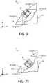
- FIG. 3 is a schematic plan view of a substrate according to the embodiment.
- a lighting device 1 As illustrated in FIG. 1 , a lighting device 1 according to the embodiment includes a substrate 10 made of a ceramic, a socket 20 for accommodating the substrate 10, and a plurality of electrically conductive terminals 30 connected to the substrate 10.
- the lighting device 1 is used, as, for example, an on-board lighting device. Specifically, the lighting device 1 is used as a light source such as a rear lamp, a turn lamp, a position lamp, and a fog lamp.
- the socket 20 includes a housing part 21, a flange part 22, and a plurality of heat dissipating fins 23.
- the housing part 21 is, for example, a bottomed tubular portion having a substantially circular shape in a plan view, and is located on a surface opposite a surface on which the plurality of heat dissipating fins 23 are located in the flange part 22 described below.
- the housing part 21 includes a recessed portion 210 recessed from an end surface of the socket 20, specifically from a surface opposite a surface in contact with the flange part 22 of the housing part 21, toward the other end side of the socket 20.
- the substrate 10 is accommodated in the recessed portion 210.
- the recessed portion 210 includes a plurality of side wall portions 211.
- the plurality of side wall portions 211 have, for example, an arcuate shape in a plan view, and are arranged along a circumferential direction around the substrate 10 so as to surround the substrate 10.
- Gaps 212 are provided each between two of the plurality of side wall portions 211 adjacent to each other in the circumferential direction.
- the flange part 22 is, for example, a disc-shaped portion, and is located between the housing part 21 and the plurality of heat dissipating fins 23.
- the flange part 22 has a larger diameter than that of the housing part 21, and when the lighting device 1 is inserted into, for example, a mounting hole provided in the vehicle body, the flange part 22 comes into contact with a peripheral edge of the mounting hole.
- a bayonet (not illustrated) for a twist lock is located on an outer peripheral surface of the housing part 21, and by rotating the socket 20 in a state where the flange part 22 is in contact with the peripheral edge of the mounting hole, the bayonet is fitted into a groove on the vehicle body side, so that the lighting device 1 is in a state of being fixed to the vehicle body.
- the plurality of heat dissipating fins 23 are located on a surface opposite a surface on which the housing part 21 is located in the flange part 22. Heat generated in the substrate 10 is emitted primarily from the plurality of heat dissipating fins 23.
- the socket 20 includes four heat dissipating fins 23, but the number of the heat dissipating fins 23 of the socket 20 is not limited to four.
- a heat transfer member (not illustrated) formed of, for example, a metal such as aluminum is located between a bottom portion of the recessed portion 210 and the substrate 10.
- the heat transfer member is located so as to be in contact with the substrate 10 and the bottom portion of the recessed portion 210, and transmits the heat generated in the substrate 10 to the heat dissipating fins 23.
- the substrate 10 is a member having a flat plate shape, and including a circuit forming surface 110 (here, a front surface) serving as a first surface, a second surface (here, a rear surface) located opposite the circuit forming surface 110, and a third surface (here, a side surface) connected to each of the circuit forming surface 110 and the second surface.
- the substrate 10 is accommodated in the housing part 21 in a state where the second surface faces the bottom surface of the recessed portion 210, in other words, in a state where the circuit forming surface 110 faces the front.
- the ceramic used for the substrate 10 examples include an aluminum oxide-based ceramic, a zirconium oxide-based ceramic, a composite ceramic of aluminum oxide and zirconium oxide, a silicon nitride-based ceramic, an aluminum nitride-based ceramic, a silicon carbide-based ceramic, and a mullite ceramic.
- the substrate 10 made of the aluminum oxide-based ceramic has mechanical strength required for the substrate 10, and has superior workability.
- the substrate 10 made of the aluminum nitride-based ceramic has high thermal conductivity, and thus has superior heat radiating properties.
- Wirings 40 containing a metal such as copper, silver, or the like as a main constituent are located on the circuit forming surface 110.
- the wirings 40 are electrically connected to electrically conductive terminals 30 via an electrically conductive bonding material (not illustrated) such as a brazing material or a solder.
- a light emitting element 50 is located on the wirings 40.
- the light emitting element 50 is, for example, a light emitting diode (LED), a laser diode (LD), or the like.
- the shape and the arrangement of the wirings 40 and the light emitting element 50 are illustrated as an example in FIG. 3 .
- the example is illustrated in which the light emitting element 50 located on one of the wirings 40 and the other one of wirings 40 are electrically connected by a bonding wire 45, but a method of connecting the wiring 40 and the light emitting element 50 is not limited to the example illustrated in FIG. 3 .
- a resistor or the like is located on the circuit forming surface 110.
- the circuit forming surface 110 of the substrate 10 includes four sides 111 and four corner portions 112.
- the four sides 111 include two first sides 111a parallel to each other and two second sides 111b parallel to each other.
- the two first sides 111a extend along the Y-axis direction
- the two second sides 111b extend along the X-axis direction.
- the first sides 111a and the second sides 111b are orthogonal to each other.
- Each of the four corner portions 112 is located between one of the first sides 111a and one of the second sides 111b.
- the two first sides 111a, the two second sides 111b, and the four corner portions 112 are continuous in the order of one of the first sides 111a, one of the corner portions 112, one of the second sides 111b, one of the corner portions 112, the other one of the first sides 111a, one of the corner portions 112, the other one of the second sides 111b, and one of the corner portions.
- the second surface of the substrate 10 has the same shape as the circuit forming surface 110.
- FIG. 4 is a schematic plan view of a lighting device according to the embodiment. Note that, in FIG. 4 , for ease of understanding, a part of a configuration of the socket 20 such as the flange part 22 is not illustrated.
- each of first side wall portions 211a facing one of the first sides 111a extend in the Y-axis direction in the same manner as the first sides 111a, and is located outward in the X-axis direction of the corresponding one of the first sides 111a.
- Each of second side wall portions 211b facing one of the second sides 111b extends in the X-axis direction in the same manner as the second sides 111b, and is located outward in the Y-axis direction of the corresponding one of the first sides 111a.
- each of the side wall portions 211 is located in the socket 20 so as to face corresponding one of the sides 111 of the substrate 10, each of sides 111 of the substrate 10 can be protected even when the lighting device 1 receives an external impact, for example.
- each of the side wall portions 211 is longer than the facing one of sides 111, an end portion of the facing one of sides 111 can be reliably protected. More specifically, since both end portions of each of the side wall portions 211 in the extending direction are located outward in the extending direction than both end portions of the facing one of the sides 111, the both end portions of the facing one of the sides 111 can be reliably protected, and thus reliability in the vibration environment of the lighting device 1 mounted on the vehicle can be improved.
- each of the side wall portions 211 By positioning each of the side wall portions 211 so as to face the corresponding one of the sides 111 of the substrate 10, the heat generated in the substrate 10 can be dissipated from each of the sides 111 of the 10j to the corresponding one of the side wall portions 211.
- each of the gaps 212 is located between side wall portions 211 adjacent to each other, that is, between one of the first side wall portions 211a and corresponding one of the second side wall portions 211b.
- the gaps 212 are provided, for example, so that the corner portions of the substrate do not interfere with the recessed portion due to the miniaturization of the socket. Further, the gaps 212 are provided, for example, to prevent the heat generated in the substrate from being kept in the recessed portion.
- Each of the gaps 212 is located between one of the first side wall portions 211a facing one of the first sides 111a and one of the second side wall portions 211b facing one of the second sides 111b.
- Each of the corner portions 112 is located between corresponding one of the first sides 111a and corresponding one of the second sides 111b.
- the corner portions 112 of the substrate 10 are exposed from the recessed portion 210.
- the corner portions 112 of the substrate 10 are considered to be more likely to be chipped or cracked by such an impact than the sides 111 of the substrate 10 protected by the side wall portions 211.
- the substrate 10 includes the corner portions 112 having an inverted-R shape curved toward the inside of the circuit forming surface 110 in a plan view of the substrate 10 from a direction perpendicular to the circuit forming surface 110.
- the corner portions 112 having the inverted-R shape have a larger margin with respect to the gaps 212 than a case where the corner portions are not chamfered or the corner portions are chamfered into a C-plane shape.
- the corner portions 112 having the inverted-R shape are located at a position further away from the gaps 212 than the case where the corner portions are not chamfered or the case where the corner portions are chamfered into the C-plane shape.
- the corner portions 112 having the inverted-R shape are less likely to be damaged over the gaps 212.
- the corner portions 112 By configuring the corner portions 112 to have the inverted-R shape, the heat capacity of the entirety of the substrate 10 can be reduced as compared with the case where the corner portions are not chamfered or the case where the corner portions are chamfered into the C-plane shape. As a result, heat accumulation in the substrate 10 can be suppressed.
- a surface area of the corner portions 112 By configuring the corner portions 112 to have the inverted-R shape, a surface area of the corner portions 112 can be increased as compared with the case where the corner portion is not chamfered or the case where the corner portion is chamfered in a C-plane shape. Accordingly, heat radiation from the corner portions 112 can be increased, and heat can be efficiently dissipated from the corner portions 112 to the exterior of the socket 20 via the gaps 212.
- the shape of the corner portions 112 when viewing the substrate 10 from a direction perpendicular to the circuit forming surface 110 corresponds to, for example, one arc (quarter arc) obtained by equally dividing one circle into four.
- the substrate used in the lighting device may be formed by obtaining a large number of substrates from one single large substrate.
- the large substrate is provided with a plurality of slits in the longitudinal direction and the horizontal direction for splitting, and by providing through-holes having circular shape at positions where the slits in the longitudinal direction and the slits in the horizontal direction intersect with each other, each of the corner portions 112 having the inverted-R shape can be formed at four corner portions of each of the substrates 10 serving as individual pieces.
- configuring of the corner portions 112 in a quarter arc shape can enhance productivity in the case where the large number of substrates 10 is obtained from the one single large substrate can be improved.
- configuring the through-holes in a circular shape cracking due to stress concentration can be less likely to occur as compared with a case where through-holes having rectangular shape are used, for example.
- FIG. 5 is a schematic plan view of a lighting device according to the first modified example.
- FIG. 6 is a schematic enlarged view of a portion H in FIG. 5 . Note that, in FIG. 5 , for ease of understanding, a part of a configuration of the socket 20 such as the flange part 22, and the wirings 40, the light emitting element 50, and the like on the substrate 10 are not illustrated.
- each of the electrically conductive terminals 30 is located in a recessed region of corresponding one of the corner portions 112.
- an example is given in which each one of the four electrically conductive terminals 30 included in the lighting device 1A is located in the recessed region of the corresponding one of the four corner portions 112.
- the four side wall portions 211 and the four electrically conductive terminals 30 are alternately arranged along the circumferential direction.
- the thermal uniformity of the substrate 10 can be increased.
- the lighting device 1A does not necessarily include the same number of electrically conductive terminals 30 as the number of the corner portions 112.
- the side wall portions 211 and the electrically conductive terminals 30 may be alternately arranged at least in part in the circumferential direction.
- each of the electrically conductive terminals 30 entirely fits in the region R1, but at least a portion of each of the electrically conductive terminals 30 may be located in the region R1. In other words, each of the electrically conductive terminals 30 may partially protrude from the region R1.
- FIG. 7 is a schematic plan view of the lighting device according to the second modified example.
- each of the electrically conductive terminals 30 is located in a recessed region of corresponding one of the corner portions 112.
- each of the first side wall portions 211a is longer than a line segment connecting intersection points 115 and 115 between a virtual extended line 113 of facing one of the first sides 111a and virtual extended lines 114 and 114 of two second sides 111b adjacent to the corresponding one of the first sides 111a via corresponding one of the corner portions 112.
- each of the second side wall portions 211b is longer than a line segment connecting intersection points 115 and 115 (one of them is not illustrated) between a virtual extended line 114 of facing one of the second sides 111b and virtual extended lines 113 and 113 (one of them is not illustrated) of two first sides 111a adjacent to the corresponding one of the second sides 111b via corresponding one of the corner portions 112.
- each of the electrically conductive terminals 30 can be covered with two side wall portions 211 (one of the first side wall portions 211a and one of the second side wall portions 211b). As a result, the reliability in the vibration environment of the lighting device 1 mounted on the vehicle can be further improved.
- each of the first side wall portions 211a may be shorter than the line segment connecting the intersection points 115 and 115 between the virtual extended line 114 of facing one of the first sides 111a and the virtual extended lines 113 and 113 of two second sides 111b adjacent to the corresponding one of the first sides 111a via corresponding one of the corner portions 112. This corresponds to, for example, the configuration illustrated in FIG. 6 .
- each of the electrically conductive terminals 30 can be protected by the two side wall portions 211 (one of the first side wall portions 211a and one of the second side wall portions 211b), and thus improving the reliability in the vibration environment of the lighting device 1.
- FIG. 8 is a schematic plan view of the lighting device according to the third modified example. Note that the periphery of the corner portion 112 is illustrated enlarged in FIG. 8 .
- the electrically conductive terminal 30 is in contact with two side wall portions 211 adjacent to each other (the first side wall portion 211a and the second side wall portion 211b).
- the vibration of the electrically conductive terminal 30 can be suppressed by the side wall portions 211. Accordingly, the reliability in the vibration environment of the lighting device 1 can be further improved. Further, when the electrically conductive terminal 30 generates heat, the heat generated at the electrically conductive terminal 30 can be efficiently dissipated to the side wall portions 211.
- FIG. 9 is a schematic plan view of the lighting device according to the fourth modified example. Note that the periphery of the corner portion 112 is illustrated enlarged in FIG. 9 .
- the electrically conductive terminal 30 is sandwiched between two adjacent side wall portions 211 (the first side wall portion 211a and the second side wall portion 211b).
- the vibration of the electrically conductive terminal 30 can be suppressed by the side wall portions 211. Further, when the electrically conductive terminal 30 generates heat, the heat generated at the electrically conductive terminal 30 can be efficiently dissipated to the side wall portions 211.
- the electrically conductive terminal 30 By sandwiching the electrically conductive terminal 30 between the two side wall portions 211, the electrically conductive terminal 30 can be fixed by the two side wall portions 211. Thus, for example, the amount of adhesive or the like used to fix the electrically conductive terminal 30 can be reduced.
- FIGS. 10 and 11 are schematic plan views of the lighting device according to the fifth modified example. Note that the periphery of the corner portion 112 is illustrated enlarged in FIG. 10 .
- the electrically conductive terminal 30 is in contact with the corner portion 112. In this way, by bringing the electrically conductive terminal 30 into contact with the corner portion 112, the vibration of the electrically conductive terminal 30 can be suppressed by the substrate 10. Accordingly, the reliability in the vibration environment of the lighting device 1 can be further improved.
- the lighting device 1E according to the fifth modified example includes two electrically conductive terminals 30, and each of the two electrically conductive terminals 30 is located in a recessed region of corresponding one of the two corner portions 112 located diagonally. With such a configuration, a position shift of the substrate 10 due to vibration or the like can be suppressed by the two electrically conductive terminals 30.
- having the inverted-R shape can suppress not only the position shift in the diagonal direction in which the two electrically conductive terminals 30 are disposed, but also the position shift in a diagonal direction orthogonal to the diagonal direction in which the two electrically conductive terminals 30 are disposed, as compared with a case in which the corner portions have the C-plane shape. Accordingly, the reliability in the vibration environment of the lighting device 1 can be further improved.
- each of the electrically conductive terminals 30 is in contact with only corresponding one of the corner portions 112, but each of the electrically conductive terminals 30 may be in contact with the corresponding one of the corner portions 112 and also in contact with the side wall portions 211.
- Each of the electrically conductive terminals 30 may be in contact with the corresponding one of the corner portions 112 and also sandwiched by two side wall portions 211 adjacent to each other. In other words, each of the electrically conductive terminals 30 may be sandwiched by the corresponding one of the corner portions 112 and the two side wall portions 211 adjacent to each other.
- FIG. 12 is a schematic plan view of the substrate according to the sixth modified example.
- a region surrounded by two virtual lines 116 and 116 connecting end points of the first sides 111a facing each other and two virtual lines 117 and 117 connecting end points of the second sides 111b facing each other is defined as a region R2.
- a circuit mounting region R3 in the circuit forming surface 110 overlaps the region R2, and extends outward from the region R2.
- the circuit mounting region R3 is longer than the region R2 in the X-axis direction and in the Y-axis direction.
- the circuit mounting region R3 can be more widely ensured in the substrate 10F including the inverted-R shaped corner portions 112.
- the circuit mounting region R3 is a region in which the wirings 40, the light emitting element 50, and the like can be mounted.
- the electronic device for example, the lighting devices 1 and 1A to IE
- the electronic device includes a substrate made of a ceramic (for example, the substrates 10 and 10F), and a housing part (for example, the housing part 21 of the socket 20) including a recessed portion (for example, the recessed portion 210) for accommodating the substrate.
- the recessed portion includes a plurality of side wall portions (for example, the four side wall portions 211) arranged along the circumferential direction around the substrate, and respectively facing one of a plurality of sides (for example, the four sides 111) of the substrate in a plan view when viewing the substrate from a direction perpendicular to a circuit forming surface (for example, the circuit forming surface 110) of the substrate, and a plurality of gaps (for example, the four gaps 212) each located between two side wall portions adjacent to each other in the circumferential direction.
- the substrate includes a plurality of corner portions (for example, the four corner portions 112), curved toward an inner side of the circuit forming surface in a plan view.
- the electronic device according to the present disclosure is not limited to the lighting device and is applicable to various electronic devices other than the lighting device.
- the electronic device is applicable to a flowmeter, a mounted display monitor, such as on a smart watch, a power module such as an inverter, a converter, or the like, a power semiconductor such as on-board power control unit, battery components, secondary battery components, air conditioning systems (particularly for on-board applications), optical communication devices, laser projectors such as laser cinemas, laser machines, various sensor components, optical pickup components used for reading and writing a digital versatile disk (DVD) or a compact disk (CD), laser diode components, laser diode components, a central processing unit (CPU), a graphics processing unit (GPU), a tensor processing unit (TPU), and the like.
- the electronic device according to the present disclosure can be suitably used for a product in which the outer shape of the substrate is square (in a case where the inverted-R shape of the corner portions is ignored), and the outer shape of the housing part accommodating the substrate is circular.
Landscapes
- Engineering & Computer Science (AREA)
- Physics & Mathematics (AREA)
- Optics & Photonics (AREA)
- Microelectronics & Electronic Packaging (AREA)
- General Engineering & Computer Science (AREA)
- Condensed Matter Physics & Semiconductors (AREA)
- General Physics & Mathematics (AREA)
- Electromagnetism (AREA)
- Chemical & Material Sciences (AREA)
- Ceramic Engineering (AREA)
- Inorganic Chemistry (AREA)
- Arrangement Of Elements, Cooling, Sealing, Or The Like Of Lighting Devices (AREA)
- Structure Of Printed Boards (AREA)
- Mounting Of Printed Circuit Boards And The Like (AREA)
- Fastening Of Light Sources Or Lamp Holders (AREA)
- Non-Portable Lighting Devices Or Systems Thereof (AREA)
Abstract
Description
- The present disclosure relates to an electronic device.
- Since a substrate made of a ceramic has superior insulating properties, superior thermal conductivity, and the like, the substrate may be utilized as a substrate for a lighting device such as an on-board lamp.
- The lighting device includes a substrate in which a light emitting element such as a light emitting diode and a wiring or the like are located, and a socket for accommodating the substrate.
- Here, Patent Document 1 discloses a socket including a notch at a location where a corner portion of a substrate is located.
- Patent Document 1:
JP 2019-102227 A - However, in the conventional technology described above, since the corner portion of the substrate is exposed, for example, when receiving an impact from outside, chips and cracks may occur in the corner portion of the substrate.
- The present disclosure has been made in view of the above, and an object thereof is to provide an electronic device which can suppress damage to the corner portion of the substrate while using a housing part in which the corner portion of the substrate is exposed.
- An electronic device according to an aspect of the present disclosure includes a substrate made of a ceramic, and a housing part including a recessed portion for accommodating the substrate. The recessed portion includes a plurality of side wall portions arranged around the substrate along a circumferential direction and respectively facing one of a plurality of sides of the substrate in a plan view when viewing the substrate from a direction perpendicular to a circuit forming surface of the substrate, and a plurality of gaps each located between two of the plurality of side wall portions adjacent to each other in the circumferential direction. The substrate includes a plurality of corner portions curved toward an inner side of the circuit forming surface in a plan view.
- According to the present disclosure, damage to a corner portion of a substrate can be suppressed while using a socket in which the corner portion of the substrate is exposed.
-
-
FIG. 1 is a schematic side view of a lighting device according to an embodiment. -
FIG. 2 is a schematic perspective view of a socket according to an embodiment. -
FIG. 3 is a schematic plan view of a substrate according to an embodiment. -
FIG. 4 is a schematic plan view of the lighting device according to the embodiment. -
FIG. 5 is a schematic plan view of a lighting device according to a first modified example. -
FIG. 6 is a schematic enlarged view of an H portion inFIG. 5 . -
FIG. 7 is a schematic plan view of a lighting device according to a second modified example. -
FIG. 8 is a schematic plan view of a lighting device according to a third modified example. -
FIG. 9 is a schematic plan view of a lighting device according to a fourth modified example. -
FIG. 10 is a schematic plan view of a lighting device according to a fifth modified example. -
FIG. 11 is a schematic plan view of the lighting device according to the fifth modified example. -
FIG. 12 is a schematic plan view of a substrate according to a sixth modified example. - Modes (hereinafter, referred to as "embodiments") for implementing an electronic device according to the present disclosure will be described in detail below with reference to the drawings. Note that the embodiments described below are not intended to limit the electronic device according to the present disclosure. Each of the embodiments can be appropriately combined within a range in which the processing contents do not contradict each other. In each of the embodiments below, the same reference numerals are assigned to the same portions, and redundant descriptions thereof will be omitted.
- In the embodiments described below, expressions such as "constant", "orthogonal", "vertical," and "parallel" may be used, but these expressions do not need to be exactly "constant", "orthogonal", "vertical," and "parallel". In other words, each of the above-described expressions allows for deviations in, for example, manufacturing accuracy, positioning accuracy, and the like.
- In each of the drawings referred below, for ease of explanation, an X-axis direction, a Y-axis direction, and a Z-axis direction that are orthogonal to each other may be defined to illustrate an orthogonal coordinate system in which the Z-axis positive direction is the vertically upward direction.
- In the embodiments described below, examples will be described in which the electronic device according to the present disclosure is applied to a lighting device.
- First, a configuration of the lighting device 1 according to an embodiment will be described with reference to
FIGS. 1 to 3 .FIG. 1 is a schematic side view illustrating the lighting device according to the embodiment.FIG. 2 is a schematic perspective view of a socket according to the embodiment.FIG. 3 is a schematic plan view of a substrate according to the embodiment. - As illustrated in
FIG. 1 , a lighting device 1 according to the embodiment includes asubstrate 10 made of a ceramic, asocket 20 for accommodating thesubstrate 10, and a plurality of electricallyconductive terminals 30 connected to thesubstrate 10. The lighting device 1 is used, as, for example, an on-board lighting device. Specifically, the lighting device 1 is used as a light source such as a rear lamp, a turn lamp, a position lamp, and a fog lamp. - As illustrated in
FIGS. 1 and 2 , thesocket 20 includes ahousing part 21, aflange part 22, and a plurality of heat dissipating fins 23. - The
housing part 21 is, for example, a bottomed tubular portion having a substantially circular shape in a plan view, and is located on a surface opposite a surface on which the plurality ofheat dissipating fins 23 are located in theflange part 22 described below. Thehousing part 21 includes arecessed portion 210 recessed from an end surface of thesocket 20, specifically from a surface opposite a surface in contact with theflange part 22 of thehousing part 21, toward the other end side of thesocket 20. Thesubstrate 10 is accommodated in therecessed portion 210. - The
recessed portion 210 includes a plurality ofside wall portions 211. The plurality ofside wall portions 211 have, for example, an arcuate shape in a plan view, and are arranged along a circumferential direction around thesubstrate 10 so as to surround thesubstrate 10. -
Gaps 212 are provided each between two of the plurality ofside wall portions 211 adjacent to each other in the circumferential direction. - The
flange part 22 is, for example, a disc-shaped portion, and is located between thehousing part 21 and the plurality of heat dissipating fins 23. Theflange part 22 has a larger diameter than that of thehousing part 21, and when the lighting device 1 is inserted into, for example, a mounting hole provided in the vehicle body, theflange part 22 comes into contact with a peripheral edge of the mounting hole. A bayonet (not illustrated) for a twist lock is located on an outer peripheral surface of thehousing part 21, and by rotating thesocket 20 in a state where theflange part 22 is in contact with the peripheral edge of the mounting hole, the bayonet is fitted into a groove on the vehicle body side, so that the lighting device 1 is in a state of being fixed to the vehicle body. - The plurality of
heat dissipating fins 23 are located on a surface opposite a surface on which thehousing part 21 is located in theflange part 22. Heat generated in thesubstrate 10 is emitted primarily from the plurality ofheat dissipating fins 23. Here, the example is given in which thesocket 20 includes four heat dissipating fins 23, but the number of the heat dissipating fins 23 of thesocket 20 is not limited to four. - Note that a heat transfer member (not illustrated) formed of, for example, a metal such as aluminum is located between a bottom portion of the
recessed portion 210 and thesubstrate 10. The heat transfer member is located so as to be in contact with thesubstrate 10 and the bottom portion of therecessed portion 210, and transmits the heat generated in thesubstrate 10 to theheat dissipating fins 23. - As illustrated in
FIG. 3 , thesubstrate 10 is a member having a flat plate shape, and including a circuit forming surface 110 (here, a front surface) serving as a first surface, a second surface (here, a rear surface) located opposite thecircuit forming surface 110, and a third surface (here, a side surface) connected to each of thecircuit forming surface 110 and the second surface. Thesubstrate 10 is accommodated in thehousing part 21 in a state where the second surface faces the bottom surface of therecessed portion 210, in other words, in a state where thecircuit forming surface 110 faces the front. - Examples of the ceramic used for the
substrate 10 include an aluminum oxide-based ceramic, a zirconium oxide-based ceramic, a composite ceramic of aluminum oxide and zirconium oxide, a silicon nitride-based ceramic, an aluminum nitride-based ceramic, a silicon carbide-based ceramic, and a mullite ceramic. Note that thesubstrate 10 made of the aluminum oxide-based ceramic has mechanical strength required for thesubstrate 10, and has superior workability. Thesubstrate 10 made of the aluminum nitride-based ceramic has high thermal conductivity, and thus has superior heat radiating properties. -
Wirings 40 containing a metal such as copper, silver, or the like as a main constituent are located on thecircuit forming surface 110. Thewirings 40 are electrically connected to electricallyconductive terminals 30 via an electrically conductive bonding material (not illustrated) such as a brazing material or a solder. - A
light emitting element 50 is located on thewirings 40. Thelight emitting element 50 is, for example, a light emitting diode (LED), a laser diode (LD), or the like. - Note that the shape and the arrangement of the
wirings 40 and thelight emitting element 50 are illustrated as an example inFIG. 3 . For example, inFIG. 3 , the example is illustrated in which thelight emitting element 50 located on one of thewirings 40 and the other one ofwirings 40 are electrically connected by abonding wire 45, but a method of connecting thewiring 40 and thelight emitting element 50 is not limited to the example illustrated inFIG. 3 . Although not illustrated here, other than thewirings 40 and thelight emitting element 50, a resistor or the like is located on thecircuit forming surface 110. - As illustrated in
FIG. 3 , thecircuit forming surface 110 of thesubstrate 10 includes foursides 111 and fourcorner portions 112. The foursides 111 include twofirst sides 111a parallel to each other and twosecond sides 111b parallel to each other. The twofirst sides 111a extend along the Y-axis direction, and the twosecond sides 111b extend along the X-axis direction. In other words, thefirst sides 111a and thesecond sides 111b are orthogonal to each other. Each of the fourcorner portions 112 is located between one of thefirst sides 111a and one of thesecond sides 111b. The twofirst sides 111a, the twosecond sides 111b, and the fourcorner portions 112 are continuous in the order of one of thefirst sides 111a, one of thecorner portions 112, one of thesecond sides 111b, one of thecorner portions 112, the other one of thefirst sides 111a, one of thecorner portions 112, the other one of thesecond sides 111b, and one of the corner portions. The second surface of thesubstrate 10 has the same shape as thecircuit forming surface 110. - Next, a relationship between the plurality of
side wall portions 211 provided in thesocket 20 and thesubstrate 10 will be described with reference toFIG. 4. FIG. 4 is a schematic plan view of a lighting device according to the embodiment. Note that, inFIG. 4 , for ease of understanding, a part of a configuration of thesocket 20 such as theflange part 22 is not illustrated. - As illustrated in
FIG. 4 , the fourside wall portions 211 of thesocket 20 respectively face corresponding one of the foursides 111 of thecircuit forming surface 110. Specifically, each of firstside wall portions 211a facing one of thefirst sides 111a extend in the Y-axis direction in the same manner as thefirst sides 111a, and is located outward in the X-axis direction of the corresponding one of thefirst sides 111a. Each of secondside wall portions 211b facing one of thesecond sides 111b extends in the X-axis direction in the same manner as thesecond sides 111b, and is located outward in the Y-axis direction of the corresponding one of thefirst sides 111a. - In this way, since each of the
side wall portions 211 is located in thesocket 20 so as to face corresponding one of thesides 111 of thesubstrate 10, each ofsides 111 of thesubstrate 10 can be protected even when the lighting device 1 receives an external impact, for example. In the embodiment, since each of theside wall portions 211 is longer than the facing one ofsides 111, an end portion of the facing one ofsides 111 can be reliably protected. More specifically, since both end portions of each of theside wall portions 211 in the extending direction are located outward in the extending direction than both end portions of the facing one of thesides 111, the both end portions of the facing one of thesides 111 can be reliably protected, and thus reliability in the vibration environment of the lighting device 1 mounted on the vehicle can be improved. - By positioning each of the
side wall portions 211 so as to face the corresponding one of thesides 111 of thesubstrate 10, the heat generated in thesubstrate 10 can be dissipated from each of thesides 111 of the 10j to the corresponding one of theside wall portions 211. - On the other hand, as described above, each of the
gaps 212 is located betweenside wall portions 211 adjacent to each other, that is, between one of the firstside wall portions 211a and corresponding one of the secondside wall portions 211b. Thegaps 212 are provided, for example, so that the corner portions of the substrate do not interfere with the recessed portion due to the miniaturization of the socket. Further, thegaps 212 are provided, for example, to prevent the heat generated in the substrate from being kept in the recessed portion. - Each of the
gaps 212 is located between one of the firstside wall portions 211a facing one of thefirst sides 111a and one of the secondside wall portions 211b facing one of thesecond sides 111b. Each of thecorner portions 112 is located between corresponding one of thefirst sides 111a and corresponding one of thesecond sides 111b. Thus, when viewing the inside of the recessedportion 210 from the side of the lighting device 1 over thegaps 212, each of thecorner portions 112 of thesubstrate 10 is located at a location visible from corresponding one of thegaps 212. - In this way, when the lighting device 1 is viewed from the side, the
corner portions 112 of thesubstrate 10 are exposed from the recessedportion 210. Thus, when the lighting device 1 receives the external impact, thecorner portions 112 of thesubstrate 10 are considered to be more likely to be chipped or cracked by such an impact than thesides 111 of thesubstrate 10 protected by theside wall portions 211. - On the other hand, as illustrated in
FIG. 3 , thesubstrate 10 according to the embodiment includes thecorner portions 112 having an inverted-R shape curved toward the inside of thecircuit forming surface 110 in a plan view of thesubstrate 10 from a direction perpendicular to thecircuit forming surface 110. - The
corner portions 112 having the inverted-R shape have a larger margin with respect to thegaps 212 than a case where the corner portions are not chamfered or the corner portions are chamfered into a C-plane shape. In other words, thecorner portions 112 having the inverted-R shape are located at a position further away from thegaps 212 than the case where the corner portions are not chamfered or the case where the corner portions are chamfered into the C-plane shape. Thus, thecorner portions 112 having the inverted-R shape are less likely to be damaged over thegaps 212. - By configuring the
corner portions 112 to have the inverted-R shape, the heat capacity of the entirety of thesubstrate 10 can be reduced as compared with the case where the corner portions are not chamfered or the case where the corner portions are chamfered into the C-plane shape. As a result, heat accumulation in thesubstrate 10 can be suppressed. By configuring thecorner portions 112 to have the inverted-R shape, a surface area of thecorner portions 112 can be increased as compared with the case where the corner portion is not chamfered or the case where the corner portion is chamfered in a C-plane shape. Accordingly, heat radiation from thecorner portions 112 can be increased, and heat can be efficiently dissipated from thecorner portions 112 to the exterior of thesocket 20 via thegaps 212. - Note that the shape of the
corner portions 112 when viewing thesubstrate 10 from a direction perpendicular to thecircuit forming surface 110 corresponds to, for example, one arc (quarter arc) obtained by equally dividing one circle into four. The substrate used in the lighting device may be formed by obtaining a large number of substrates from one single large substrate. The large substrate is provided with a plurality of slits in the longitudinal direction and the horizontal direction for splitting, and by providing through-holes having circular shape at positions where the slits in the longitudinal direction and the slits in the horizontal direction intersect with each other, each of thecorner portions 112 having the inverted-R shape can be formed at four corner portions of each of thesubstrates 10 serving as individual pieces. In this way, configuring of thecorner portions 112 in a quarter arc shape can enhance productivity in the case where the large number ofsubstrates 10 is obtained from the one single large substrate can be improved. By configuring the through-holes in a circular shape, cracking due to stress concentration can be less likely to occur as compared with a case where through-holes having rectangular shape are used, for example. - Next, a modified example of the lighting device 1 according to the embodiments described above will be described below. First, the configuration example of a lighting device according to a first modified example will be described with reference to
FIGS. 5 and 6. FIG. 5 is a schematic plan view of a lighting device according to the first modified example.FIG. 6 is a schematic enlarged view of a portion H inFIG. 5 . Note that, inFIG. 5 , for ease of understanding, a part of a configuration of thesocket 20 such as theflange part 22, and thewirings 40, thelight emitting element 50, and the like on thesubstrate 10 are not illustrated. - As illustrated in
FIG. 5 , in alighting device 1A according to the first modified example, each of the electricallyconductive terminals 30 is located in a recessed region of corresponding one of thecorner portions 112. Here, an example is given in which each one of the four electricallyconductive terminals 30 included in thelighting device 1A is located in the recessed region of the corresponding one of the fourcorner portions 112. - In this way, by positioning each of the electrically
conductive terminals 30 in the recessed region of the corresponding one of thecorner portions 112, the circuit mounting region of thecircuit forming surface 110 can be more widely ensured than a case where the electricallyconductive terminals 30 are located on thecircuit forming surface 110 of thesubstrate 10. - As illustrated in
FIG. 5 , in thelighting device 1A, the fourside wall portions 211 and the four electricallyconductive terminals 30 are alternately arranged along the circumferential direction. By alternately arranging theside wall portions 211 and the electricallyconductive terminals 30, since the heat generation points are dispersed as compared with a case where, for example, the plurality of electricallyconductive terminals 30 are concentrated in one place, the thermal uniformity of thesubstrate 10 can be increased. Note that thelighting device 1A does not necessarily include the same number of electricallyconductive terminals 30 as the number of thecorner portions 112. In other words, theside wall portions 211 and the electricallyconductive terminals 30 may be alternately arranged at least in part in the circumferential direction. - As illustrated in
FIG. 6 , the recessed region of each of thecorner portions 112 corresponds to a region R1 surrounded by virtualextended lines first sides 111a and one of thesecond sides 111b adjacent to one of thecorner portions 112 and the one of thecorner portions 112. Here, an example is given in which each of the electricallyconductive terminals 30 entirely fits in the region R1, but at least a portion of each of the electricallyconductive terminals 30 may be located in the region R1. In other words, each of the electricallyconductive terminals 30 may partially protrude from the region R1. - Next, a configuration example of a lighting device according to a second modified example will be described with reference to
FIG. 7. FIG. 7 is a schematic plan view of the lighting device according to the second modified example. - As illustrated in
FIG. 7 , in alighting device 1B according to the second modified example, similar to thelighting device 1A according to the first modified example, each of the electricallyconductive terminals 30 is located in a recessed region of corresponding one of thecorner portions 112. - In the
lighting device 1B according to the second modified example, for example, each of the firstside wall portions 211a is longer than a line segment connecting intersection points 115 and 115 between a virtualextended line 113 of facing one of thefirst sides 111a and virtualextended lines second sides 111b adjacent to the corresponding one of thefirst sides 111a via corresponding one of thecorner portions 112. The same applies to the secondside wall portions 211b, and each of the secondside wall portions 211b is longer than a line segment connecting intersection points 115 and 115 (one of them is not illustrated) between a virtualextended line 114 of facing one of thesecond sides 111b and virtualextended lines 113 and 113 (one of them is not illustrated) of twofirst sides 111a adjacent to the corresponding one of thesecond sides 111b via corresponding one of thecorner portions 112. - With such a configuration, substantially the entirety of each of the electrically
conductive terminals 30 can be covered with two side wall portions 211 (one of the firstside wall portions 211a and one of the secondside wall portions 211b). As a result, the reliability in the vibration environment of the lighting device 1 mounted on the vehicle can be further improved. - Note that the
side wall portions 211 may be configured to cover a portion of each of the electricallyconductive terminals 30. For example, each of the firstside wall portions 211a may be shorter than the line segment connecting the intersection points 115 and 115 between the virtualextended line 114 of facing one of thefirst sides 111a and the virtualextended lines second sides 111b adjacent to the corresponding one of thefirst sides 111a via corresponding one of thecorner portions 112. This corresponds to, for example, the configuration illustrated inFIG. 6 . Even with such a configuration, each of the electricallyconductive terminals 30 can be protected by the two side wall portions 211 (one of the firstside wall portions 211a and one of the secondside wall portions 211b), and thus improving the reliability in the vibration environment of the lighting device 1. - Next, a configuration of a lighting device according to a third modified example will be described with reference to
FIG. 8. FIG. 8 is a schematic plan view of the lighting device according to the third modified example. Note that the periphery of thecorner portion 112 is illustrated enlarged inFIG. 8 . - As illustrated in
FIG. 8 , in a lighting device 1C according to the third modified example, the electricallyconductive terminal 30 is in contact with twoside wall portions 211 adjacent to each other (the firstside wall portion 211a and the secondside wall portion 211b). In this way, by bringing the electrically conductive terminal 30 into contact with theside wall portions 211, for example, the vibration of the electrically conductive terminal 30 can be suppressed by theside wall portions 211. Accordingly, the reliability in the vibration environment of the lighting device 1 can be further improved. Further, when the electricallyconductive terminal 30 generates heat, the heat generated at the electrically conductive terminal 30 can be efficiently dissipated to theside wall portions 211. - Next, a configuration of a lighting device according to a fourth modified example will be described with reference to
FIG. 9. FIG. 9 is a schematic plan view of the lighting device according to the fourth modified example. Note that the periphery of thecorner portion 112 is illustrated enlarged inFIG. 9 . - As illustrated in
FIG. 9 , in alighting device 1D according to the fourth modified example, the electricallyconductive terminal 30 is sandwiched between two adjacent side wall portions 211 (the firstside wall portion 211a and the secondside wall portion 211b). - In this way, by sandwiching the electrically conductive terminal 30 between the two
side wall portions 211, similar to the lighting device 1C according to the third modified example, the vibration of the electrically conductive terminal 30 can be suppressed by theside wall portions 211. Further, when the electricallyconductive terminal 30 generates heat, the heat generated at the electrically conductive terminal 30 can be efficiently dissipated to theside wall portions 211. - By sandwiching the electrically conductive terminal 30 between the two
side wall portions 211, the electrically conductive terminal 30 can be fixed by the twoside wall portions 211. Thus, for example, the amount of adhesive or the like used to fix the electrically conductive terminal 30 can be reduced. - Next, a configuration of a lighting device according to a fifth modified example will be described with reference to
FIGS. 10 and11 .FIGS. 10 and11 are schematic plan views of the lighting device according to the fifth modified example. Note that the periphery of thecorner portion 112 is illustrated enlarged inFIG. 10 . - As illustrated in
FIG. 10 , in alighting device 1E according to the fifth modified example, the electricallyconductive terminal 30 is in contact with thecorner portion 112. In this way, by bringing the electrically conductive terminal 30 into contact with thecorner portion 112, the vibration of the electrically conductive terminal 30 can be suppressed by thesubstrate 10. Accordingly, the reliability in the vibration environment of the lighting device 1 can be further improved. - As illustrated in
FIG. 11 , thelighting device 1E according to the fifth modified example includes two electricallyconductive terminals 30, and each of the two electricallyconductive terminals 30 is located in a recessed region of corresponding one of the twocorner portions 112 located diagonally. With such a configuration, a position shift of thesubstrate 10 due to vibration or the like can be suppressed by the two electricallyconductive terminals 30. Specifically, in thecorner portions 112, having the inverted-R shape can suppress not only the position shift in the diagonal direction in which the two electricallyconductive terminals 30 are disposed, but also the position shift in a diagonal direction orthogonal to the diagonal direction in which the two electricallyconductive terminals 30 are disposed, as compared with a case in which the corner portions have the C-plane shape. Accordingly, the reliability in the vibration environment of the lighting device 1 can be further improved. - Here, the example is given in which each of the electrically
conductive terminals 30 is in contact with only corresponding one of thecorner portions 112, but each of the electricallyconductive terminals 30 may be in contact with the corresponding one of thecorner portions 112 and also in contact with theside wall portions 211. Each of the electricallyconductive terminals 30 may be in contact with the corresponding one of thecorner portions 112 and also sandwiched by twoside wall portions 211 adjacent to each other. In other words, each of the electricallyconductive terminals 30 may be sandwiched by the corresponding one of thecorner portions 112 and the twoside wall portions 211 adjacent to each other. - Next, a configuration of a substrate according to a sixth modified example will be described with reference to
FIG. 12. FIG. 12 is a schematic plan view of the substrate according to the sixth modified example. - As illustrated in
FIG. 12 , a region surrounded by twovirtual lines first sides 111a facing each other and twovirtual lines second sides 111b facing each other is defined as a region R2. In asubstrate 10F according to the sixth modified example, a circuit mounting region R3 in thecircuit forming surface 110 overlaps the region R2, and extends outward from the region R2. Specifically, the circuit mounting region R3 is longer than the region R2 in the X-axis direction and in the Y-axis direction. - As described above, by disposing the circuit mounting region R3 outward from the region R2, the circuit mounting region R3 can be more widely ensured in the
substrate 10F including the inverted-R shapedcorner portions 112. Note that the circuit mounting region R3 is a region in which thewirings 40, thelight emitting element 50, and the like can be mounted. - As described above, the electronic device (for example, the
lighting devices 1 and 1A to IE) according to the embodiments includes a substrate made of a ceramic (for example, thesubstrates housing part 21 of the socket 20) including a recessed portion (for example, the recessed portion 210) for accommodating the substrate. The recessed portion includes a plurality of side wall portions (for example, the four side wall portions 211) arranged along the circumferential direction around the substrate, and respectively facing one of a plurality of sides (for example, the four sides 111) of the substrate in a plan view when viewing the substrate from a direction perpendicular to a circuit forming surface (for example, the circuit forming surface 110) of the substrate, and a plurality of gaps (for example, the four gaps 212) each located between two side wall portions adjacent to each other in the circumferential direction. The substrate includes a plurality of corner portions (for example, the four corner portions 112), curved toward an inner side of the circuit forming surface in a plan view. - As described above, with the electronic device according to the embodiments, by configuring the corner portions of the substrate in the inverted-R shape, damage to the corner portions of the substrate can be suppressed while using the housing part with the exposed corner portions of the substrate.
- The electronic device according to the present disclosure is not limited to the lighting device and is applicable to various electronic devices other than the lighting device.
- For example, the electronic device according to the present disclosure is applicable to a flowmeter, a mounted display monitor, such as on a smart watch, a power module such as an inverter, a converter, or the like, a power semiconductor such as on-board power control unit, battery components, secondary battery components, air conditioning systems (particularly for on-board applications), optical communication devices, laser projectors such as laser cinemas, laser machines, various sensor components, optical pickup components used for reading and writing a digital versatile disk (DVD) or a compact disk (CD), laser diode components, laser diode components, a central processing unit (CPU), a graphics processing unit (GPU), a tensor processing unit (TPU), and the like. In particular, the electronic device according to the present disclosure can be suitably used for a product in which the outer shape of the substrate is square (in a case where the inverted-R shape of the corner portions is ignored), and the outer shape of the housing part accommodating the substrate is circular.
- Additional effects and variations can be easily derived by a person skilled in the art. Thus, a wide variety of aspects of the present invention are not limited to the specific details and representative embodiments represented and described above. Accordingly, various changes are possible without departing from the spirit or scope of the general inventive concepts defined by the appended claims and their equivalents.
-
- 1 Lighting device
- 10 Substrate
- 110 Circuit forming surface
- 111 Side
- 112 Corner portion
- 20 Socket
- 21 Housing part
- 210 Recessed portion
- 211 Side wall portion
- 212 Gap
- 22 Flange part
- 23 Heat dissipating fin
- 30 Electrically conductive terminal
- 40 Wiring
- 45 Bonding wire
- 50 Light emitting element
Claims (11)
- An electronic device comprising:a substrate made of a ceramic; anda housing part comprising a recessed portion configured to accommodate the substrate, whereinthe recessed portion comprisesa plurality of side wall portions arranged around the substrate along a circumferential direction and respectively facing a plurality of sides of the substrate in a plan view when viewing the substrate from a direction perpendicular to a circuit forming surface of the substrate, anda plurality of gaps each located between two of the plurality of side wall portions adjacent to each other in the circumferential direction, andthe substrate comprises a plurality of corner portions curved toward an inner side of the circuit forming surface in the plan view.
- The electronic device according to claim 1, wherein
each of the plurality of side wall portions is longer than a facing one of the plurality of sides. - The electronic device according to claim 1 or 2, further comprising:wiring located on the circuit forming surface; andan electrically conductive terminal connected to the wiring, whereinat least a portion of the electrically conductive terminal is located in a recessed region of each of the plurality of corner portions.
- The electronic device according to claim 3, wherein
the recessed region is a region surrounded by virtual extended lines of two of the plurality of sides adjacent to corresponding one of the plurality of corner portions and the corresponding one of the plurality of corner portions. - The electronic device according to claim 3 or 4, wherein
each of the plurality of side wall portions is longer than the facing one of the plurality of sides, and shorter than a line segment connecting intersection points between a virtual extended line of the corresponding one of the plurality of sides and virtual extended lines of two of the plurality of sides adjacent to the corresponding one of the plurality of sides via the corresponding one of the plurality of corner portions. - The electronic device according to claim 3 or 4, wherein
each of the plurality of side wall portions is longer than a line segment connecting intersection points between a virtual extended line of the facing one of the plurality of sides and virtual extended lines of two of the plurality of sides adjacent to the corresponding one of the plurality of sides via the corresponding one of the plurality of corner portions. - The electronic device according to any one of claims 3 to 6, wherein
the electrically conductive terminal is in contact with the plurality of side wall portions. - The electronic device according to claim 7, wherein
the electrically conductive terminal is sandwiched between two of the plurality of side wall portions adjacent to each other. - The electronic device according to any one of claims 3 to 8, further comprising:a plurality of the electrically conductive terminals, whereinthe plurality of side wall portions and the plurality of electrically conductive terminals are alternately arranged at least in part in the circumferential direction.
- The electronic device according to any one of claims 3 to 9, further comprising:
two of the electrically conductive terminals in contact with respective two of the plurality of corner portions located diagonally. - The electronic device according to any one of claims 1 to 10, wherein
the substrate comprises, in the plan view, a circuit mounting region outward of a region surrounded by two virtual lines connecting end points of two first sides facing each other of the plurality of sides and two virtual lines connecting end points of two second sides facing each other and orthogonal to the first sides of the plurality of sides.
Applications Claiming Priority (2)
| Application Number | Priority Date | Filing Date | Title |
|---|---|---|---|
| JP2019154451 | 2019-08-27 | ||
| PCT/JP2020/025597 WO2021039096A1 (en) | 2019-08-27 | 2020-06-29 | Electronic device |
Publications (3)
| Publication Number | Publication Date |
|---|---|
| EP4024483A1 true EP4024483A1 (en) | 2022-07-06 |
| EP4024483A4 EP4024483A4 (en) | 2023-09-13 |
| EP4024483B1 EP4024483B1 (en) | 2024-11-06 |
Family
ID=74683654
Family Applications (1)
| Application Number | Title | Priority Date | Filing Date |
|---|---|---|---|
| EP20858508.3A Active EP4024483B1 (en) | 2019-08-27 | 2020-06-29 | Electronic device |
Country Status (5)
| Country | Link |
|---|---|
| US (1) | US11805599B2 (en) |
| EP (1) | EP4024483B1 (en) |
| JP (1) | JP7268170B2 (en) |
| CN (1) | CN114342096A (en) |
| WO (1) | WO2021039096A1 (en) |
Family Cites Families (18)
| Publication number | Priority date | Publication date | Assignee | Title |
|---|---|---|---|---|
| DE60026331T8 (en) | 1999-10-01 | 2007-02-01 | Seiko Epson Corp. | PCB, SEMICONDUCTOR AND MANUFACTURING, TEST AND HOUSING OF THE SAME AND SYSTEM BOARD AND ELECTRONIC UNIT |
| US7293898B2 (en) * | 2004-07-29 | 2007-11-13 | Princeton Tectonics, Inc. | Portable light |
| JP2006196703A (en) * | 2005-01-13 | 2006-07-27 | Epson Toyocom Corp | Surface mount electronic devices |
| WO2007128070A1 (en) * | 2006-05-10 | 2007-11-15 | Spa Electrics Pty Ltd | Assembly including a fastening device |
| JP5469177B2 (en) * | 2009-09-30 | 2014-04-09 | パナソニック株式会社 | Lighting device |
| US8568001B2 (en) | 2012-02-03 | 2013-10-29 | Tyco Electronics Corporation | LED socket assembly |
| JP5914920B2 (en) * | 2012-02-28 | 2016-05-11 | 東芝ライテック株式会社 | Light emitting module, lamp device and lighting device |
| CN102903831A (en) * | 2012-05-15 | 2013-01-30 | 北京工业大学 | White LED structure and production process thereof |
| JP6094202B2 (en) * | 2012-12-19 | 2017-03-15 | 市光工業株式会社 | Light source unit of semiconductor light source for vehicle lamp, vehicle lamp |
| CN105471405B (en) * | 2014-09-30 | 2018-08-28 | 日本特殊陶业株式会社 | Circuit board and more formula circuit boards in flakes |
| JP2016095284A (en) * | 2014-11-17 | 2016-05-26 | セイコーエプソン株式会社 | Electronic devices, physical quantity sensors, pressure sensors, altimeters, electronic equipment, and moving objects |
| KR20170033947A (en) * | 2015-09-17 | 2017-03-28 | 삼성전자주식회사 | Light source module and lighting device having the same |
| KR102406627B1 (en) * | 2015-10-21 | 2022-06-08 | 엘지이노텍 주식회사 | Camera Module |
| WO2017209149A1 (en) * | 2016-05-31 | 2017-12-07 | シチズン電子株式会社 | Light-emitting device |
| EP3550618B1 (en) * | 2016-11-29 | 2020-10-07 | KYOCERA Corporation | Thermoelectric module |
| JP6645413B2 (en) * | 2016-12-15 | 2020-02-14 | 豊田合成株式会社 | Electronic equipment |
| JP6811940B2 (en) * | 2017-03-21 | 2021-01-13 | 東芝ライテック株式会社 | Vehicle lighting and vehicle lighting |
| JP6969328B2 (en) | 2017-11-30 | 2021-11-24 | 東芝ライテック株式会社 | Vehicle lighting equipment and vehicle lighting equipment |
-
2020
- 2020-06-29 US US17/638,075 patent/US11805599B2/en active Active
- 2020-06-29 WO PCT/JP2020/025597 patent/WO2021039096A1/en not_active Ceased
- 2020-06-29 CN CN202080059691.6A patent/CN114342096A/en active Pending
- 2020-06-29 EP EP20858508.3A patent/EP4024483B1/en active Active
- 2020-06-29 JP JP2021542578A patent/JP7268170B2/en active Active
Also Published As
| Publication number | Publication date |
|---|---|
| WO2021039096A1 (en) | 2021-03-04 |
| US20220279650A1 (en) | 2022-09-01 |
| US11805599B2 (en) | 2023-10-31 |
| EP4024483A4 (en) | 2023-09-13 |
| JP7268170B2 (en) | 2023-05-02 |
| CN114342096A (en) | 2022-04-12 |
| JPWO2021039096A1 (en) | 2021-03-04 |
| EP4024483B1 (en) | 2024-11-06 |
Similar Documents
| Publication | Publication Date | Title |
|---|---|---|
| KR102129647B1 (en) | Optoelectronic lighting module, optoelectronic lighting device, and motor vehicle headlamp | |
| US9829165B2 (en) | LED support with wire-bonded electrical connection for a lighting module of a motor vehicle and electrical connector by wire-bonding | |
| US11309680B2 (en) | Light source device including lead terminals that cross space defined by base and cap | |
| US20150338079A1 (en) | Lighting device with at least one semiconductor light source | |
| US9608172B2 (en) | Optoelectronic semiconductor component | |
| CN113451879A (en) | Semiconductor package header and semiconductor package | |
| CN105972533A (en) | Light source module | |
| TWI446516B (en) | Photoelectric component and method of making optoelectronic component | |
| CN115986553B (en) | Laser system | |
| US11805599B2 (en) | Electronic device | |
| JP6225834B2 (en) | Semiconductor light emitting device and manufacturing method thereof | |
| CN103814440A (en) | Electrical control device with moulded housing | |
| JP7321282B2 (en) | Circuit boards and electronic devices | |
| JP7597996B2 (en) | Light-emitting device | |
| US20240414846A1 (en) | Substrate module or light emitting module | |
| JP7416818B2 (en) | circuit boards and electronic devices | |
| JP7174230B2 (en) | Light source device | |
| JP2017069109A (en) | Light source device | |
| EP3703115B1 (en) | Semiconductor device | |
| JP7021444B2 (en) | Luminous module | |
| US20080056315A1 (en) | Semiconductor laser device | |
| US20250008660A1 (en) | Circuit substrate and electronic device | |
| TW201532208A (en) | Light-emitting element mounting substrate and light-emitting device using the same | |
| CN205026596U (en) | Lighting device | |
| US20240023241A1 (en) | Circuit substrate and electronic device |
Legal Events
| Date | Code | Title | Description |
|---|---|---|---|
| STAA | Information on the status of an ep patent application or granted ep patent |
Free format text: STATUS: THE INTERNATIONAL PUBLICATION HAS BEEN MADE |
|
| PUAI | Public reference made under article 153(3) epc to a published international application that has entered the european phase |
Free format text: ORIGINAL CODE: 0009012 |
|
| STAA | Information on the status of an ep patent application or granted ep patent |
Free format text: STATUS: REQUEST FOR EXAMINATION WAS MADE |
|
| 17P | Request for examination filed |
Effective date: 20220222 |
|
| AK | Designated contracting states |
Kind code of ref document: A1 Designated state(s): AL AT BE BG CH CY CZ DE DK EE ES FI FR GB GR HR HU IE IS IT LI LT LU LV MC MK MT NL NO PL PT RO RS SE SI SK SM TR |
|
| DAV | Request for validation of the european patent (deleted) | ||
| DAX | Request for extension of the european patent (deleted) | ||
| P01 | Opt-out of the competence of the unified patent court (upc) registered |
Effective date: 20230505 |
|
| A4 | Supplementary search report drawn up and despatched |
Effective date: 20230811 |
|
| RIC1 | Information provided on ipc code assigned before grant |
Ipc: F21S 45/48 20180101ALI20230808BHEP Ipc: F21S 41/19 20180101ALI20230808BHEP Ipc: F21S 41/143 20180101ALI20230808BHEP Ipc: H05K 1/18 20060101ALI20230808BHEP Ipc: H05K 1/03 20060101ALI20230808BHEP Ipc: H05K 1/02 20060101ALI20230808BHEP Ipc: H01S 5/022 20210101ALI20230808BHEP Ipc: H01L 33/62 20100101ALI20230808BHEP Ipc: H01L 33/00 20100101ALI20230808BHEP Ipc: F21V 19/00 20060101ALI20230808BHEP Ipc: F21S 43/19 20180101ALI20230808BHEP Ipc: F21S 43/14 20180101ALI20230808BHEP Ipc: H01L 33/48 20100101AFI20230808BHEP |
|
| GRAP | Despatch of communication of intention to grant a patent |
Free format text: ORIGINAL CODE: EPIDOSNIGR1 |
|
| STAA | Information on the status of an ep patent application or granted ep patent |
Free format text: STATUS: GRANT OF PATENT IS INTENDED |
|
| INTG | Intention to grant announced |
Effective date: 20240603 |
|
| GRAS | Grant fee paid |
Free format text: ORIGINAL CODE: EPIDOSNIGR3 |
|
| GRAA | (expected) grant |
Free format text: ORIGINAL CODE: 0009210 |
|
| STAA | Information on the status of an ep patent application or granted ep patent |
Free format text: STATUS: THE PATENT HAS BEEN GRANTED |
|
| AK | Designated contracting states |
Kind code of ref document: B1 Designated state(s): AL AT BE BG CH CY CZ DE DK EE ES FI FR GB GR HR HU IE IS IT LI LT LU LV MC MK MT NL NO PL PT RO RS SE SI SK SM TR |
|
| REG | Reference to a national code |
Ref country code: GB Ref legal event code: FG4D |
|
| REG | Reference to a national code |
Ref country code: CH Ref legal event code: EP |
|
| REG | Reference to a national code |
Ref country code: DE Ref legal event code: R079 Ref document number: 602020041009 Country of ref document: DE Free format text: PREVIOUS MAIN CLASS: H01L0033480000 Ipc: H10H0020850000 |
|
| REG | Reference to a national code |
Ref country code: DE Ref legal event code: R096 Ref document number: 602020041009 Country of ref document: DE |
|
| REG | Reference to a national code |
Ref country code: IE Ref legal event code: FG4D |
|
| REG | Reference to a national code |
Ref country code: LT Ref legal event code: MG9D |
|
| REG | Reference to a national code |
Ref country code: NL Ref legal event code: MP Effective date: 20241106 |
|
| PG25 | Lapsed in a contracting state [announced via postgrant information from national office to epo] |
Ref country code: IS Free format text: LAPSE BECAUSE OF FAILURE TO SUBMIT A TRANSLATION OF THE DESCRIPTION OR TO PAY THE FEE WITHIN THE PRESCRIBED TIME-LIMIT Effective date: 20250306 Ref country code: HR Free format text: LAPSE BECAUSE OF FAILURE TO SUBMIT A TRANSLATION OF THE DESCRIPTION OR TO PAY THE FEE WITHIN THE PRESCRIBED TIME-LIMIT Effective date: 20241106 Ref country code: PT Free format text: LAPSE BECAUSE OF FAILURE TO SUBMIT A TRANSLATION OF THE DESCRIPTION OR TO PAY THE FEE WITHIN THE PRESCRIBED TIME-LIMIT Effective date: 20250306 |
|
| PG25 | Lapsed in a contracting state [announced via postgrant information from national office to epo] |
Ref country code: NL Free format text: LAPSE BECAUSE OF FAILURE TO SUBMIT A TRANSLATION OF THE DESCRIPTION OR TO PAY THE FEE WITHIN THE PRESCRIBED TIME-LIMIT Effective date: 20241106 Ref country code: FI Free format text: LAPSE BECAUSE OF FAILURE TO SUBMIT A TRANSLATION OF THE DESCRIPTION OR TO PAY THE FEE WITHIN THE PRESCRIBED TIME-LIMIT Effective date: 20241106 |
|
| REG | Reference to a national code |
Ref country code: AT Ref legal event code: MK05 Ref document number: 1740392 Country of ref document: AT Kind code of ref document: T Effective date: 20241106 |
|
| PG25 | Lapsed in a contracting state [announced via postgrant information from national office to epo] |
Ref country code: BG Free format text: LAPSE BECAUSE OF FAILURE TO SUBMIT A TRANSLATION OF THE DESCRIPTION OR TO PAY THE FEE WITHIN THE PRESCRIBED TIME-LIMIT Effective date: 20241106 |
|
| PG25 | Lapsed in a contracting state [announced via postgrant information from national office to epo] |
Ref country code: ES Free format text: LAPSE BECAUSE OF FAILURE TO SUBMIT A TRANSLATION OF THE DESCRIPTION OR TO PAY THE FEE WITHIN THE PRESCRIBED TIME-LIMIT Effective date: 20241106 |
|
| PG25 | Lapsed in a contracting state [announced via postgrant information from national office to epo] |
Ref country code: NO Free format text: LAPSE BECAUSE OF FAILURE TO SUBMIT A TRANSLATION OF THE DESCRIPTION OR TO PAY THE FEE WITHIN THE PRESCRIBED TIME-LIMIT Effective date: 20250206 |
|
| PG25 | Lapsed in a contracting state [announced via postgrant information from national office to epo] |
Ref country code: LV Free format text: LAPSE BECAUSE OF FAILURE TO SUBMIT A TRANSLATION OF THE DESCRIPTION OR TO PAY THE FEE WITHIN THE PRESCRIBED TIME-LIMIT Effective date: 20241106 Ref country code: AT Free format text: LAPSE BECAUSE OF FAILURE TO SUBMIT A TRANSLATION OF THE DESCRIPTION OR TO PAY THE FEE WITHIN THE PRESCRIBED TIME-LIMIT Effective date: 20241106 Ref country code: GR Free format text: LAPSE BECAUSE OF FAILURE TO SUBMIT A TRANSLATION OF THE DESCRIPTION OR TO PAY THE FEE WITHIN THE PRESCRIBED TIME-LIMIT Effective date: 20250207 |
|
| PG25 | Lapsed in a contracting state [announced via postgrant information from national office to epo] |
Ref country code: PL Free format text: LAPSE BECAUSE OF FAILURE TO SUBMIT A TRANSLATION OF THE DESCRIPTION OR TO PAY THE FEE WITHIN THE PRESCRIBED TIME-LIMIT Effective date: 20241106 |
|
| PG25 | Lapsed in a contracting state [announced via postgrant information from national office to epo] |
Ref country code: RS Free format text: LAPSE BECAUSE OF FAILURE TO SUBMIT A TRANSLATION OF THE DESCRIPTION OR TO PAY THE FEE WITHIN THE PRESCRIBED TIME-LIMIT Effective date: 20250206 |
|
| PG25 | Lapsed in a contracting state [announced via postgrant information from national office to epo] |
Ref country code: SM Free format text: LAPSE BECAUSE OF FAILURE TO SUBMIT A TRANSLATION OF THE DESCRIPTION OR TO PAY THE FEE WITHIN THE PRESCRIBED TIME-LIMIT Effective date: 20241106 |
|
| PGFP | Annual fee paid to national office [announced via postgrant information from national office to epo] |
Ref country code: DE Payment date: 20250507 Year of fee payment: 6 |
|
| PG25 | Lapsed in a contracting state [announced via postgrant information from national office to epo] |
Ref country code: DK Free format text: LAPSE BECAUSE OF FAILURE TO SUBMIT A TRANSLATION OF THE DESCRIPTION OR TO PAY THE FEE WITHIN THE PRESCRIBED TIME-LIMIT Effective date: 20241106 |
|
| PG25 | Lapsed in a contracting state [announced via postgrant information from national office to epo] |
Ref country code: EE Free format text: LAPSE BECAUSE OF FAILURE TO SUBMIT A TRANSLATION OF THE DESCRIPTION OR TO PAY THE FEE WITHIN THE PRESCRIBED TIME-LIMIT Effective date: 20241106 |
|
| PG25 | Lapsed in a contracting state [announced via postgrant information from national office to epo] |
Ref country code: RO Free format text: LAPSE BECAUSE OF FAILURE TO SUBMIT A TRANSLATION OF THE DESCRIPTION OR TO PAY THE FEE WITHIN THE PRESCRIBED TIME-LIMIT Effective date: 20241106 |
|
| PG25 | Lapsed in a contracting state [announced via postgrant information from national office to epo] |
Ref country code: SK Free format text: LAPSE BECAUSE OF FAILURE TO SUBMIT A TRANSLATION OF THE DESCRIPTION OR TO PAY THE FEE WITHIN THE PRESCRIBED TIME-LIMIT Effective date: 20241106 |
|
| PG25 | Lapsed in a contracting state [announced via postgrant information from national office to epo] |
Ref country code: CZ Free format text: LAPSE BECAUSE OF FAILURE TO SUBMIT A TRANSLATION OF THE DESCRIPTION OR TO PAY THE FEE WITHIN THE PRESCRIBED TIME-LIMIT Effective date: 20241106 |
|
| PG25 | Lapsed in a contracting state [announced via postgrant information from national office to epo] |
Ref country code: IT Free format text: LAPSE BECAUSE OF FAILURE TO SUBMIT A TRANSLATION OF THE DESCRIPTION OR TO PAY THE FEE WITHIN THE PRESCRIBED TIME-LIMIT Effective date: 20241106 |
|
| REG | Reference to a national code |
Ref country code: DE Ref legal event code: R097 Ref document number: 602020041009 Country of ref document: DE |
|
| PG25 | Lapsed in a contracting state [announced via postgrant information from national office to epo] |
Ref country code: SE Free format text: LAPSE BECAUSE OF FAILURE TO SUBMIT A TRANSLATION OF THE DESCRIPTION OR TO PAY THE FEE WITHIN THE PRESCRIBED TIME-LIMIT Effective date: 20241106 |
|
| PLBE | No opposition filed within time limit |
Free format text: ORIGINAL CODE: 0009261 |
|
| STAA | Information on the status of an ep patent application or granted ep patent |
Free format text: STATUS: NO OPPOSITION FILED WITHIN TIME LIMIT |
|
| 26N | No opposition filed |
Effective date: 20250807 |
|
| REG | Reference to a national code |
Ref country code: CH Ref legal event code: H13 Free format text: ST27 STATUS EVENT CODE: U-0-0-H10-H13 (AS PROVIDED BY THE NATIONAL OFFICE) Effective date: 20260127 |
|
| PG25 | Lapsed in a contracting state [announced via postgrant information from national office to epo] |
Ref country code: MC Free format text: LAPSE BECAUSE OF FAILURE TO SUBMIT A TRANSLATION OF THE DESCRIPTION OR TO PAY THE FEE WITHIN THE PRESCRIBED TIME-LIMIT Effective date: 20241106 |
|
| PG25 | Lapsed in a contracting state [announced via postgrant information from national office to epo] |
Ref country code: LU Free format text: LAPSE BECAUSE OF NON-PAYMENT OF DUE FEES Effective date: 20250629 |
|
| GBPC | Gb: european patent ceased through non-payment of renewal fee |
Effective date: 20250629 |
|
| REG | Reference to a national code |
Ref country code: BE Ref legal event code: MM Effective date: 20250630 |
|
| PG25 | Lapsed in a contracting state [announced via postgrant information from national office to epo] |
Ref country code: GB Free format text: LAPSE BECAUSE OF NON-PAYMENT OF DUE FEES Effective date: 20250629 |
|
| PG25 | Lapsed in a contracting state [announced via postgrant information from national office to epo] |
Ref country code: IE Free format text: LAPSE BECAUSE OF NON-PAYMENT OF DUE FEES Effective date: 20250629 |
|
| PG25 | Lapsed in a contracting state [announced via postgrant information from national office to epo] |
Ref country code: BE Free format text: LAPSE BECAUSE OF NON-PAYMENT OF DUE FEES Effective date: 20250630 |
|
| PG25 | Lapsed in a contracting state [announced via postgrant information from national office to epo] |
Ref country code: FR Free format text: LAPSE BECAUSE OF NON-PAYMENT OF DUE FEES Effective date: 20250630 |
|
| PG25 | Lapsed in a contracting state [announced via postgrant information from national office to epo] |
Ref country code: CH Free format text: LAPSE BECAUSE OF NON-PAYMENT OF DUE FEES Effective date: 20250630 |