EP4024416A1 - Coil driving device - Google Patents
Coil driving device Download PDFInfo
- Publication number
- EP4024416A1 EP4024416A1 EP20856676.0A EP20856676A EP4024416A1 EP 4024416 A1 EP4024416 A1 EP 4024416A1 EP 20856676 A EP20856676 A EP 20856676A EP 4024416 A1 EP4024416 A1 EP 4024416A1
- Authority
- EP
- European Patent Office
- Prior art keywords
- impedance
- pwm signal
- unit
- pwm
- driving device
- Prior art date
- Legal status (The legal status is an assumption and is not a legal conclusion. Google has not performed a legal analysis and makes no representation as to the accuracy of the status listed.)
- Granted
Links
Images



Classifications
-
- H—ELECTRICITY
- H01—ELECTRIC ELEMENTS
- H01F—MAGNETS; INDUCTANCES; TRANSFORMERS; SELECTION OF MATERIALS FOR THEIR MAGNETIC PROPERTIES
- H01F7/00—Magnets
- H01F7/06—Electromagnets; Actuators including electromagnets
- H01F7/08—Electromagnets; Actuators including electromagnets with armatures
- H01F7/18—Circuit arrangements for obtaining desired operating characteristics, e.g. for slow operation, for sequential energisation of windings, for high-speed energisation of windings
- H01F7/1844—Monitoring or fail-safe circuits
-
- H—ELECTRICITY
- H01—ELECTRIC ELEMENTS
- H01F—MAGNETS; INDUCTANCES; TRANSFORMERS; SELECTION OF MATERIALS FOR THEIR MAGNETIC PROPERTIES
- H01F7/00—Magnets
- H01F7/06—Electromagnets; Actuators including electromagnets
- H01F7/064—Circuit arrangements for actuating electromagnets
-
- H—ELECTRICITY
- H01—ELECTRIC ELEMENTS
- H01F—MAGNETS; INDUCTANCES; TRANSFORMERS; SELECTION OF MATERIALS FOR THEIR MAGNETIC PROPERTIES
- H01F7/00—Magnets
- H01F7/06—Electromagnets; Actuators including electromagnets
- H01F7/08—Electromagnets; Actuators including electromagnets with armatures
- H01F7/16—Rectilinearly-movable armatures
-
- H—ELECTRICITY
- H01—ELECTRIC ELEMENTS
- H01F—MAGNETS; INDUCTANCES; TRANSFORMERS; SELECTION OF MATERIALS FOR THEIR MAGNETIC PROPERTIES
- H01F7/00—Magnets
- H01F7/06—Electromagnets; Actuators including electromagnets
- H01F7/08—Electromagnets; Actuators including electromagnets with armatures
- H01F7/18—Circuit arrangements for obtaining desired operating characteristics, e.g. for slow operation, for sequential energisation of windings, for high-speed energisation of windings
- H01F7/1805—Circuit arrangements for holding the operation of electromagnets or for holding the armature in attracted position with reduced energising current
-
- H—ELECTRICITY
- H01—ELECTRIC ELEMENTS
- H01H—ELECTRIC SWITCHES; RELAYS; SELECTORS; EMERGENCY PROTECTIVE DEVICES
- H01H1/00—Contacts
- H01H1/50—Means for increasing contact pressure, preventing vibration of contacts, holding contacts together after engagement, or biasing contacts to the open position
- H01H1/54—Means for increasing contact pressure, preventing vibration of contacts, holding contacts together after engagement, or biasing contacts to the open position by magnetic force
-
- H—ELECTRICITY
- H01—ELECTRIC ELEMENTS
- H01H—ELECTRIC SWITCHES; RELAYS; SELECTORS; EMERGENCY PROTECTIVE DEVICES
- H01H47/00—Circuit arrangements not adapted to a particular application of the relay and designed to obtain desired operating characteristics or to provide energising current
- H01H47/22—Circuit arrangements not adapted to a particular application of the relay and designed to obtain desired operating characteristics or to provide energising current for supplying energising current for relay coil
-
- H—ELECTRICITY
- H01—ELECTRIC ELEMENTS
- H01F—MAGNETS; INDUCTANCES; TRANSFORMERS; SELECTION OF MATERIALS FOR THEIR MAGNETIC PROPERTIES
- H01F7/00—Magnets
- H01F7/06—Electromagnets; Actuators including electromagnets
- H01F7/08—Electromagnets; Actuators including electromagnets with armatures
- H01F7/18—Circuit arrangements for obtaining desired operating characteristics, e.g. for slow operation, for sequential energisation of windings, for high-speed energisation of windings
- H01F2007/1888—Circuit arrangements for obtaining desired operating characteristics, e.g. for slow operation, for sequential energisation of windings, for high-speed energisation of windings using pulse width modulation
-
- H—ELECTRICITY
- H01—ELECTRIC ELEMENTS
- H01H—ELECTRIC SWITCHES; RELAYS; SELECTORS; EMERGENCY PROTECTIVE DEVICES
- H01H47/00—Circuit arrangements not adapted to a particular application of the relay and designed to obtain desired operating characteristics or to provide energising current
- H01H47/002—Monitoring or fail-safe circuits
-
- H—ELECTRICITY
- H01—ELECTRIC ELEMENTS
- H01H—ELECTRIC SWITCHES; RELAYS; SELECTORS; EMERGENCY PROTECTIVE DEVICES
- H01H47/00—Circuit arrangements not adapted to a particular application of the relay and designed to obtain desired operating characteristics or to provide energising current
- H01H47/22—Circuit arrangements not adapted to a particular application of the relay and designed to obtain desired operating characteristics or to provide energising current for supplying energising current for relay coil
- H01H47/32—Energising current supplied by semiconductor device
- H01H47/325—Energising current supplied by semiconductor device by switching regulator
Definitions
- the present disclosure relates to a coil driving device, and more particularly, to a coil driving device that is easy to provide a predetermined inrush current and a latching current in a wide voltage range.
- an internal coil acts as an actuator, and when a current flows at the coil, a switch operates to conduct electricity.
- the MC is a device that turns on and off a load current by an external signal, and uses the principle of an electromagnet.
- the MC includes a fixed core at which a coil is wound, and a moving core that is moved by a magnetic force of the fixed core.
- a magnetic force is generated by the fixed core.
- the moving core is then brought into contact with the fixed core by the magnetic force such that predetermined contacts can substantially be in contact with each other.
- power is off, the magnetic force is lost, and the predetermined contacts are separated from each other by a restoration spring attached to the moving core.
- the magnetic force is proportional to a current flowing at the coil.
- a magnitude of the coil current is maintained constantly even at a variation of an input voltage, the magnetic force is also maintained constantly. Therefore, in order to maintain operating characteristics of the MC constantly, the magnitude of the current should be controlled to be constant. Moreover, since a required magnetic force when the contacts are separated is different from that when the contacts are in contact, a current control is needed for an efficient control of such different magnetic forces.
- a pulse width modulation (hereinafter referred to as 'PWM') control method by a detection of a coil current is used.
- the PWM control compares a set current value with a detected current value to adjust On/Off time of a current switching element (pulse width adjustment). When the On time extends, an amount of current increases. On the other hand, When the Off time extends, an amount of current decreases.
- a PWM circuit adjusts an amount of current by switching a power semiconductor element (Power Transistor) for adjusting a pulse width.
- a power semiconductor element Power Transistor
- a current sensor resistor, etc.
- a feedback circuit for monitoring the coil current.
- a photo coupler for monitoring the coil current.
- a high inrush current for driving the coil is required, and after operation, a change to a latching current lower than the inrush current is required to maintain an electrical connection of the MC or the moving core at an inner side of the coil. Also, since a high current at latching is not required, the current should be lowered to reduce a coil temperature.
- An aspect of the present disclosure is to provide a coil driving device capable of easily supplying predetermined inrush current and latching current in a wide voltage range.
- Another aspect of the present disclosure is to provide a coil driving device which is insensitive to temperature changes so as to secure high reliability even when temperature of a coil rises while supplying predetermined inrush current and latching current.
- a coil driving device may an input voltage sensing unit for detecting an input voltage, a switch unit configured to make a switching operation to supply a driving current to a coil, a pulse width modulation (PWM) circuit unit for outputting a PWM signal for the switching operation of the switch unit, an impedance adjustment unit for changing an impedance value such that the PWM signal is adjusted, thereby limiting the driving current, and a control unit for causing the impedance adjustment unit to change the impedance value on the basis of the input voltage, thereby adjusting at least one of the duty ratio of the PWM signal and the frequency thereof
- PWM pulse width modulation
- the driving current may include at least one of an inrush current for initial driving of a moving contactor or a moving core included in the coil, and a latching current for maintaining contact of the moving contactor or the moving core.
- the PWM circuit unit may output the PWM signal including at least one of a first PWM signal for supplying the inrush current and a second PWM signal for supplying the latching current.
- the impedance adjustment unit may include a first impedance unit having a first impedance value, a second impedance unit having a second impedance value smaller than the first impedance value, and a time delay unit to delay a point of time to supply the second PWM signal after the first PWM signal changed by the first and second impedance units is supplied to a switching element.
- the first and second impedance units may be connected in parallel to each other.
- the first impedance unit may include a first resistor having the first impedance value and a first switch connected to the first resistor
- the second impedance unit may include a second resistor having the second impedance value and a second switch connected to the second resistor.
- the first and second impedance units may vary the impedance value according to the first and second impedance values so as to adjust at least one of the duty ratio and the frequency of the PWM signal.
- the control unit may include a determination unit to determine to which one of set first, second, and third voltage ranges the input voltage belongs, and a driving control unit to control the first and second impedance units and the time delay unit according to a determination result of the determination unit.
- the driving control unit may turn off the first and second switches to maintain the impedance value as a high impedance, such that the first PWM signal for supplying the inrush current is maintained at a high level, control the time delay unit to delay a point of time after the first PWM signal is supplied, and then turn on the second switch to supply the second PWM signal for supplying the latching current.
- the driving control unit may turn off the first switch and turn on the second switch to maintain the impedance value as a medium impedance by the second impedance value such that the first PWM signal for supplying the inrush current is supplied, control the time delay unit to delay a point of time after the first PWM signal is supplied, and then turn on the second switch such that the second PWM signal for supplying the latching current is supplied.
- the driving control unit may turn off the first switch and turn on the second switch to maintain the impedance value as a medium impedance by the second impedance value such that the first PWM signal for supplying the inrush current is supplied, control the time delay unit to delay a point of time after the first PWM signal is supplied, then turn on the first and second switches such that the second PWM signal for supplying the latching current is supplied, and thus vary the impedance value as a low impedance by the first and second impedance value.
- the driving control unit may control the first and second PWM signals such that a duty ratio thereof is shortened and a frequency level is lowered as the voltage range to which the input voltage belongs changes from the first voltage range to the third voltage range.
- the coil driving device may further include a rectifier to output the input voltage rectified from an alternating-current (AC) voltage to a direct current (DC) type.
- AC alternating-current
- DC direct current
- the input voltage sensing unit may include a voltage sensor to detect the input voltage.
- the switch unit may be turned on and off by the PWM signal varied by the impedance adjustment unit.
- the impedance adjustment unit may include a plurality of impedance units, and a time delay unit to delay a point of time to supply the PWM signal changed by the plurality of impedance units.
- the plurality of impedance units may have different impedance values.
- a coil driving device can stably supply an inrush current and a latching current in a wide voltage range, thereby securing reliability of a product.
- the coil driving device can supply stable inrush current and latching current by changing a pulse width or frequency input to the PWM circuit according to an input voltage, thereby solving problems of operation at a low voltage, coil stress and life extension, and heat generation at a high voltage.
- the coil driving device can be designed to allow a capacitor for rectifying an AC voltage to a DC voltage to operate even in a rectifying circuit having many small capacitors, namely, ripples, thereby reducing size and cost.
- the coil driving device does not need a current sensor (resistor, etc.), a feedback circuit, a photo coupler, and the like for monitoring a coil current, which are required in the related art, thereby simplifying and miniaturizing a product.
- FIG. 1 is a control block diagram illustrating a control configuration of a coil driving device for a magnetic contactor and a relay according to the present disclosure
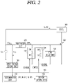
- FIG. 2 is a circuit diagram illustrating a coil driving device for a magnetic contactor and a relay according to the present disclosure.
- the coil driving device 100 for a magnetic contactor and a relay may include an input voltage sensing unit 110, a PWM circuit unit 120, an impedance adjustment unit 130, a switch unit 140, and a control unit 150.
- the input voltage sensing unit 110 may detect an input voltage Vin inputted from a power source unit Vcc.
- the power source unit Vcc may be a battery or a DC/DC converter which outputs a DC-type input voltage Vin, but may not be limited thereto.
- the power source unit Vcc may include a rectifier for rectifying an input AC voltage into a DC-type input voltage Vin.
- the input voltage sensing unit 110 may be a voltage sensor for detecting the input voltage Vin, but may not be limited thereto.
- the voltage sensor may measure a current corresponding to the input voltage Vin to detect the input voltage Vin.
- a pulse width modulation (PWM) circuit unit 120 may output a PWM signal to supply an inrush current Ip for initial driving of a moving contactor or a moving core included in a coil 160 and a latching current Id for holding contact of the moving contactor or the moving core.
- PWM pulse width modulation
- the PWM signal pwm may include a first PWM signal pwm_1 for supplying the inrush current Ip and a second PWM signal pwm_2 for supplying the latching current Id.
- the PWM circuit unit 120 may be implemented as a single PWM element, and may output a PWM signal pwm depending on a control of the control unit 150.
- the impedance adjustment unit 130 may vary at least one of a duty ratio and a frequency of the PWM signal pwm output from the PWM circuit unit 120 to supply to the switch unit 140.
- the impedance adjustment unit 130 may include first and second impedance units 132 and 134 and a time delay unit 136.
- the first impedance unit 132 may include a first switch SW1 and a first resistor R1.
- the second impedance unit 134 may be connected in parallel with the first impedance unit 132 and may include a second switch SW2 and a second resistor R2.
- the first impedance unit 132 may have a first impedance value
- the second impedance unit 134 may have a second impedance value that is smaller than the first impedance value. That is, the first resistor R1 may have a resistance value that is larger than that of the second resistor R2.
- the time delay unit 136 may delay a point of time to supply the second PWM signal pwm_2 after the first PWM signal pwm_1 is supplied.
- the switch unit 140 may be turned on and off by the PWM signal pwm.
- the PWM signal pwm may be a signal output to the PWM circuit unit 120 or a signal changed by the impedance adjustment unit 130, but may not be limited thereto.
- the switch unit 140 may be switched on and off by the PWM signal pwm to supply the inrush current Ip and the latching current Id to the coil 160.
- a diode D may be connected between the PWM circuit unit 120 and the switch unit 140.
- the diode D may be used to prevent a surge voltage from being supplied to the PWM circuit unit 120.
- the control unit 150 may include a determination unit 152 and a driving control unit 154.
- the determination unit 152 may determine to which one of set first, second, and third voltage ranges the input voltage Vin detected at the input voltage sensing unit 110 belongs.
- the second voltage range may represent a reference voltage range
- the first voltage range may be a low voltage range lower than the reference voltage range
- the third voltage range may be a high voltage range higher than the reference voltage range.
- the determination unit 152 may output a first determination signal sp1 when the input voltage Vin belongs to the first voltage range, a second determination signal sp2 when the input voltage Vin belongs to the second voltage range, and a third determination signal sp3 when the input voltage Vin belongs to the third voltage range.
- the driving control unit 154 may control the impedance adjustment unit 130 according to a determination result of the determination unit 152.
- the driving control unit 154 may control the first and second switches SW1 and SW2 to be turned off such that the first PWM signal pwm_1 for supplying the inrush current Ip is maintained at a high level.
- the driving control unit 154 may supply the first PWM signal pwm_1, control the time delay unit 136 to delay a point of time, and then turn on the second switch SW2 such that the second PWM signal pwm_2 for supplying the latching current Id is supplied. This can lower the frequency level of the second PWM signal pwm_2.
- an impedance may be adjusted according to a second impedance value of the second resistor R2, such that the frequency level of the second PWM signal pwm_2 can be adjusted to be lower than the frequency level of a second PWM signal pwm_2, which is output from the PWM circuit unit 120.
- the driving control unit 154 may turn off the first switch SW1 and turn on the second switch SW2 such that the first PWM signal pwm_1 for supplying the inrush current Ip is supplied.
- the driving control unit 154 may supply the first PWM signal pwm_1, control the time delay unit 136 to delay a point of time, and turn on the second switch SW2 such that the second PWM signal pwm_2 for supplying the latching current Id is supplied. This can lower the frequency level of the second PWM signal pwm_2.
- an impedance may be adjusted according to the second impedance value of the second resistor R2, such that the frequency level of the second PWM pwm_2 can be adjusted to be lower than the frequency level of the second PWM signal pwm_2, which is output from the PWM circuit unit 120.
- the driving control unit 154 may turn off the first switch SW1 and turn on the second switch SW2 such that the first PWM signal pwm_1 for supplying the inrush current Ip is supplied.
- the driving control unit 154 may supply the first PWM signal pwm_1, control the time delay unit 136 to delay a point of time, and turn on the first and second switches SW1 and SW2 such that the second PWM signal pwm_2 for supplying the latching current Id is supplied. This can lower the frequency level of the second PWM signal pwm_2.
- an impedance may be adjusted according to the first and second impedance values of the first and second resistors R1 and R2, such that the frequency level of the second PWM signal pwm_2 can be adjusted to be lower than the frequency level of the second PWM signal pwm_2, which is output from the PWM circuit unit 120.
- the PWM signal pwm may be adjusted such that the frequency level is lowered and the duty ratio is shortened.
- the input voltage Vin has been described to belong to any one of the first to third voltage ranges. However, but the input voltage Vin may be interpreted as belonging to any of three or more voltage ranges, and the present disclosure may not be limited thereto.
- FIG. 3 is an operation circuit diagram illustrating an implementation of a coil driving device for a magnetic contactor and a relay according to the present disclosure
- FIG. 4 illustrates a PWM signal and a PWM signal inputted to a switch unit in the operation circuit diagram of FIG. 3 .
- FIGS. 3 and 4 illustrate a circuit operation and a PWM signal when the input voltage Vin belongs to the first voltage range.
- the PWM circuit unit 120 may output the first PWM signal pwm_1 for supplying the inrush current Ip for initial driving of the moving contactor or the moving core included in the coil 160 according to the input voltage Vin.
- the control unit 150 may confirm that the input voltage Vin is lower than a normal voltage.
- the control unit 150 may control the first and second switches SW1 and SW2 to be turned off such that the frequency level of the first PWM signal pwm_1 is maintained at a high level.
- the diode D may be connected between the PWM circuit unit 120 and the switch unit 140.
- the diode D may be used to prevent a surge voltage from being supplied to the PWM circuit unit 120.
- the frequency level of the first PWM signal pwm_1 may be maintained at the high level by at least one of a capacitor and an inductor disposed at a rear end of the time delay unit 136, and may not be limited thereto.
- the frequency level of the first PWM signal pm_1 inputted to the switch unit 140 may be maintained at the high level.
- the time delay unit 136 may delay a point of time.
- the PWM circuit unit 120 may then output the second PWM signal pwm_2 such that the latching current Id for maintaining the contact of the moving contactor or the moving core is supplied.
- the control unit 150 may turn on the second switch SW2 such that the second PWM signal pwm_2 is supplied, so as to lower the frequency level of the second PWM signal pwm_2.
- the impedance when the second switch SW2 is turned on, the impedance may be adjusted according to the second impedance value by the second resistor R2, such that the frequency level of the second PWM signal pwm_2 can be adjusted to be lower than the frequency level of the second PWM signal pwm_2, which is output from the PWM circuit unit 120.
- the frequency level of the second PWM signal pwm_2 output from the PWM circuit unit 120 may be a high level, but the frequency level of the second PWM signal pwm_2 supplied to the switch unit 140 may be varied to be lower than the high level.
- FIG. 5 is an operation circuit diagram illustrating a second implementation of a coil driving device for a magnetic contactor and a relay according to the present disclosure
- FIG. 6 illustrates a PWM signal and a PWM signal inputted to a switch unit in the operation circuit diagram of FIG. 5 .
- FIGS. 5 and 6 illustrate a circuit operation and a PWM signal when the input voltage Vin belongs to the second voltage range.
- the PWM circuit unit 120 may output the first PWM signal pwm_1 for supplying the inrush current Ip for initial driving of the moving contactor or the moving core included in the coil 160 according to the input voltage Vin.
- the control unit 150 may confirm that the input voltage Vin is a normal voltage.
- the control unit 150 may turn off the first switch SW1 and turn on the second switch SW2 such that the first PWM signal pwm_1 is supplied to the switch unit 140.
- the first PWM signal pwm_1 may be outputted with a frequency and a duty ratio.
- the impedance may be varied according to the second impedance value by the second resistor R2 and thus the frequency level of the first PWM signal pm_1 inputted to the switch unit 140 may be lowered.
- the first PWM signal pwm_1 may be supplied, the time delay unit 136 may delay a point of time, and the PWM circuit unit 120 may then output the second PWM signal pwm_2 such that the latching current Id for maintaining the contact of the moving contactor or the moving core is supplied.
- the control unit 150 may turn on the second switch SW2 such that the second PWM signal pwm_2 is supplied, so as to lower the frequency level of the second PWM signal pwm_2.
- the impedance when the second switch SW2 is turned on, the impedance may be adjusted according to the second impedance value of the second resistor R2, such that the frequency level of the second PWM signal pwm_2 can be adjusted to be lower than the frequency level of the second PWM signal pwm_2, which is output from the PWM circuit unit 120.
- the frequency level of the second PWM signal pwm_2 outputted from the PWM circuit unit 120 may be a high level, but the frequency level of the second PWM signal pwm_2 supplied to the switch unit 140 can be varied to be lower than the high level.
- FIG. 7 is an operation circuit diagram illustrating a second implementation of a coil driving device for a magnetic contactor and a relay according to the present disclosure
- FIG. 8 illustrates a PWM signal and a PWM signal inputted to a switch unit in the operation circuit diagram of FIG. 7 .
- FIGS. 7 and 8 illustrate a circuit operation and a PWM signal when the input voltage Vin belongs to the third voltage range.
- the PWM circuit unit 120 may output the first PWM signal pwm_1 for supplying the inrush current Ip for initial driving of the moving contactor or the moving core included in the coil 160 according to the input voltage Vin.
- the control unit may confirm that the input voltage Vin is an overvoltage.
- the control unit 150 may turn off the first switch SW1 and turn on the second switch SW2 such that the first PWM signal pwm_1 is supplied to the switch unit 140.
- the first PWM signal pwm_1 may be outputted with a frequency and a duty ratio.
- the impedance may be varied according to the second impedance value of the second resistor R2 and thus the frequency level of the first PWM signal pm_1 inputted to the switch unit 140 may be lowered.
- the first PWM signal pwm_1 may be supplied, the time delay unit 136 may delay a point of time, and the PWM circuit unit 120 may output the second PWM signal pwm_2 such that the latching current Id for maintaining the contact of the moving contactor or the moving core is supplied.
- the control unit 150 may turn on the first and second switches SW1 and SW2 such that the second PWM signal pwm_2 is supplied, so as to lower the frequency level of the second PWM signal pwm_2.
- the impedance may be adjusted according to the first and second impedance values of the first and second resistors R1 and R2, such that the frequency level of the second PWM signal pwm_2 can be adjusted to be lower than the frequency level of the second PWM signal pwm_2, which is output from the PWM circuit unit 120.
- the frequency level of the second PWM signal pwm_2 outputted from the PWM circuit unit 120 may be a high level, but the frequency level of the second PWM signal pwm_2 supplied to the switch unit 140 may vary to be lower than the frequency level of the second PWM signal pwm_2 illustrated in FIG. 6 .
- At least one of the duty ratio and the frequency may vary depending on the input voltage Vin. Accordingly, even when the input voltage Vin is changed, the inrush current Ip and the latching current Id inputted to the coil 160 can be maintained constantly.
Landscapes
- Physics & Mathematics (AREA)
- Electromagnetism (AREA)
- Engineering & Computer Science (AREA)
- Power Engineering (AREA)
- Relay Circuits (AREA)
- Dc-Dc Converters (AREA)
Abstract
Description
- The present disclosure relates to a coil driving device, and more particularly, to a coil driving device that is easy to provide a predetermined inrush current and a latching current in a wide voltage range.
- In a Magnetic Contactor (hereinafter referred to as 'MC') and a relay, an internal coil acts as an actuator, and when a current flows at the coil, a switch operates to conduct electricity.
- Here, the MC is a device that turns on and off a load current by an external signal, and uses the principle of an electromagnet.
- The MC includes a fixed core at which a coil is wound, and a moving core that is moved by a magnetic force of the fixed core. When power is on, a magnetic force is generated by the fixed core. The moving core is then brought into contact with the fixed core by the magnetic force such that predetermined contacts can substantially be in contact with each other. When power is off, the magnetic force is lost, and the predetermined contacts are separated from each other by a restoration spring attached to the moving core.
- In an initial state in which the fixed core and the moving core are separated from each other, a large magnetic force is required to draw the moving core in an opposite direction to an action force of the spring for restoration during an initial operation time by turning power on. After the fixed core and the moving core are in contact with each other, that is, after the contacts are brought into contact with each other, the state is continuously maintained even by a small magnetic force.
- The magnetic force is proportional to a current flowing at the coil. When a magnitude of the coil current is maintained constantly even at a variation of an input voltage, the magnetic force is also maintained constantly. Therefore, in order to maintain operating characteristics of the MC constantly, the magnitude of the current should be controlled to be constant. Moreover, since a required magnetic force when the contacts are separated is different from that when the contacts are in contact, a current control is needed for an efficient control of such different magnetic forces.
- For the current control, a pulse width modulation (hereinafter referred to as 'PWM') control method by a detection of a coil current is used. The PWM control compares a set current value with a detected current value to adjust On/Off time of a current switching element (pulse width adjustment). When the On time extends, an amount of current increases. On the other hand, When the Off time extends, an amount of current decreases.
- Generally, a PWM circuit according to the PWM control method adjusts an amount of current by switching a power semiconductor element (Power Transistor) for adjusting a pulse width.
- In addition, a current sensor (resistor, etc.), a feedback circuit, a photo coupler, and the like for monitoring the coil current are required.
- In the MC and the relay, a high inrush current for driving the coil is required, and after operation, a change to a latching current lower than the inrush current is required to maintain an electrical connection of the MC or the moving core at an inner side of the coil. Also, since a high current at latching is not required, the current should be lowered to reduce a coil temperature.
- Recently, in a low voltage region or a high voltage region of an input voltage, since the PWM circuit has a limit at a maximum duty ratio of a pulse width, research has been conducted to solve a problem of an insufficient supply of current to the coil due to a limit to a driving current required at the low voltage region, and problems of increased power consumption, heat generation, and lifespan of the coil due to an increase in current at the high voltage region.
- An aspect of the present disclosure is to provide a coil driving device capable of easily supplying predetermined inrush current and latching current in a wide voltage range.
- Another aspect of the present disclosure is to provide a coil driving device which is insensitive to temperature changes so as to secure high reliability even when temperature of a coil rises while supplying predetermined inrush current and latching current.
- Implementations described herein are not limited to those aspects, and other aspects and advantages not mentioned herein will be understood by the description below and more clearly understood by the implementations of the present disclosure. Further, it will be known easily that those aspects and advantages of the present disclosure can be realized by solutions described in claims and combinations thereof.
- A coil driving device according to the present disclosure may an input voltage sensing unit for detecting an input voltage, a switch unit configured to make a switching operation to supply a driving current to a coil, a pulse width modulation (PWM) circuit unit for outputting a PWM signal for the switching operation of the switch unit, an impedance adjustment unit for changing an impedance value such that the PWM signal is adjusted, thereby limiting the driving current, and a control unit for causing the impedance adjustment unit to change the impedance value on the basis of the input voltage, thereby adjusting at least one of the duty ratio of the PWM signal and the frequency thereof
- The driving current may include at least one of an inrush current for initial driving of a moving contactor or a moving core included in the coil, and a latching current for maintaining contact of the moving contactor or the moving core.
- The PWM circuit unit may output the PWM signal including at least one of a first PWM signal for supplying the inrush current and a second PWM signal for supplying the latching current.
- The impedance adjustment unit may include a first impedance unit having a first impedance value, a second impedance unit having a second impedance value smaller than the first impedance value, and a time delay unit to delay a point of time to supply the second PWM signal after the first PWM signal changed by the first and second impedance units is supplied to a switching element.
- The first and second impedance units may be connected in parallel to each other. The first impedance unit may include a first resistor having the first impedance value and a first switch connected to the first resistor, and the second impedance unit may include a second resistor having the second impedance value and a second switch connected to the second resistor.
- When the first and second switches make the switching operation according to a control of the control unit, the first and second impedance units may vary the impedance value according to the first and second impedance values so as to adjust at least one of the duty ratio and the frequency of the PWM signal.
- The control unit may include a determination unit to determine to which one of set first, second, and third voltage ranges the input voltage belongs, and a driving control unit to control the first and second impedance units and the time delay unit according to a determination result of the determination unit.
- When it is determined that the input voltage belongs to the first voltage range, the driving control unit may turn off the first and second switches to maintain the impedance value as a high impedance, such that the first PWM signal for supplying the inrush current is maintained at a high level, control the time delay unit to delay a point of time after the first PWM signal is supplied, and then turn on the second switch to supply the second PWM signal for supplying the latching current.
- When it is determined that the input voltage belongs to the second voltage range, the driving control unit may turn off the first switch and turn on the second switch to maintain the impedance value as a medium impedance by the second impedance value such that the first PWM signal for supplying the inrush current is supplied, control the time delay unit to delay a point of time after the first PWM signal is supplied, and then turn on the second switch such that the second PWM signal for supplying the latching current is supplied.
- When it is determined that the input voltage belongs to the third voltage range, the driving control unit may turn off the first switch and turn on the second switch to maintain the impedance value as a medium impedance by the second impedance value such that the first PWM signal for supplying the inrush current is supplied, control the time delay unit to delay a point of time after the first PWM signal is supplied, then turn on the first and second switches such that the second PWM signal for supplying the latching current is supplied, and thus vary the impedance value as a low impedance by the first and second impedance value.
- The driving control unit may control the first and second PWM signals such that a duty ratio thereof is shortened and a frequency level is lowered as the voltage range to which the input voltage belongs changes from the first voltage range to the third voltage range.
- In addition, the coil driving device according to the present disclosure may further include a rectifier to output the input voltage rectified from an alternating-current (AC) voltage to a direct current (DC) type.
- The input voltage sensing unit may include a voltage sensor to detect the input voltage.
- The switch unit may be turned on and off by the PWM signal varied by the impedance adjustment unit.
- The impedance adjustment unit may include a plurality of impedance units, and a time delay unit to delay a point of time to supply the PWM signal changed by the plurality of impedance units. The plurality of impedance units may have different impedance values.
- A coil driving device according to the present disclosure can stably supply an inrush current and a latching current in a wide voltage range, thereby securing reliability of a product.
- In addition, the coil driving device according to the present disclosure can supply stable inrush current and latching current by changing a pulse width or frequency input to the PWM circuit according to an input voltage, thereby solving problems of operation at a low voltage, coil stress and life extension, and heat generation at a high voltage.
- Further, the coil driving device according to the present disclosure can be designed to allow a capacitor for rectifying an AC voltage to a DC voltage to operate even in a rectifying circuit having many small capacitors, namely, ripples, thereby reducing size and cost.
- Furthermore, the coil driving device according to the present disclosure does not need a current sensor (resistor, etc.), a feedback circuit, a photo coupler, and the like for monitoring a coil current, which are required in the related art, thereby simplifying and miniaturizing a product.
- In addition to the above-described effects, detailed effects of the present disclosure will be described together while a detailed description of the present disclosure is given.
-
-
FIG. 1 is a control block diagram illustrating a control configuration of a coil driving device for a magnetic contactor and a relay according to the present disclosure. -
FIG. 2 is a circuit diagram illustrating a coil driving device for a magnetic contactor and a relay according to the present disclosure. -
FIG. 3 is an operation circuit diagram illustrating a first implementation of a coil driving device for a magnetic contactor and a relay according to the present disclosure. -
FIG. 4 illustrates a PWM signal and a PWM signal inputted to a switch unit in the operation circuit diagram ofFIG. 3 . -
FIG. 5 is an operation circuit diagram illustrating a second implementation of a coil driving device for a magnetic contactor and a relay according to the present disclosure. -
FIG. 6 is a PWM signal and a PWM signal inputted to a switch unit in the operation circuit diagram ofFIG. 5 . -
FIG. 7 is an operation circuit diagram illustrating a third implementation of a coil driving device for a magnetic contactor and a relay according to the present disclosure. -
FIG. 8 is a PWM signal and a PWM signal inputted to a switch unit in the operation circuit diagram ofFIG. 7 . - It should be noted that, in the following description, only parts necessary for understanding the implementations of the present disclosure will be described, and descriptions of other parts will be omitted so as not to obscure the gist of the present disclosure.
- The terms or words used in this specification and claims described below should not be construed as being limited to their ordinary or dictionary meanings, and but be construed as meanings and concepts consistent with the technical idea based on the principle that it the inventors can define appropriate terms for explaining the invention in the best way. Therefore, the implementations described in this specification and the configurations illustrated in the drawings are merely illustrative and do not represent all of the technical ideas of the present disclosure, so it should be understood that various equivalents and modified implementations can replace them at the time that this application is filed.
- Hereinafter, implementations of the present disclosure will be described in more detail with reference to the accompanying drawings.
-
FIG. 1 is a control block diagram illustrating a control configuration of a coil driving device for a magnetic contactor and a relay according to the present disclosure, andFIG. 2 is a circuit diagram illustrating a coil driving device for a magnetic contactor and a relay according to the present disclosure. - Referring to
FIGS. 1 and2 , thecoil driving device 100 for a magnetic contactor and a relay may include an inputvoltage sensing unit 110, aPWM circuit unit 120, animpedance adjustment unit 130, aswitch unit 140, and acontrol unit 150. - The input
voltage sensing unit 110 may detect an input voltage Vin inputted from a power source unit Vcc. In an implementation, the power source unit Vcc may be a battery or a DC/DC converter which outputs a DC-type input voltage Vin, but may not be limited thereto. - In addition, the power source unit Vcc may include a rectifier for rectifying an input AC voltage into a DC-type input voltage Vin.
- The input
voltage sensing unit 110 may be a voltage sensor for detecting the input voltage Vin, but may not be limited thereto. Here, the voltage sensor may measure a current corresponding to the input voltage Vin to detect the input voltage Vin. - A pulse width modulation (PWM)
circuit unit 120 may output a PWM signal to supply an inrush current Ip for initial driving of a moving contactor or a moving core included in acoil 160 and a latching current Id for holding contact of the moving contactor or the moving core. - Here, the PWM signal pwm may include a first PWM signal pwm_1 for supplying the inrush current Ip and a second PWM signal pwm_2 for supplying the latching current Id.
- The
PWM circuit unit 120 may be implemented as a single PWM element, and may output a PWM signal pwm depending on a control of thecontrol unit 150. - The
impedance adjustment unit 130 may vary at least one of a duty ratio and a frequency of the PWM signal pwm output from thePWM circuit unit 120 to supply to theswitch unit 140. - First, the
impedance adjustment unit 130 may include first andsecond impedance units time delay unit 136. - The
first impedance unit 132 may include a first switch SW1 and a first resistor R1. Thesecond impedance unit 134 may be connected in parallel with thefirst impedance unit 132 and may include a second switch SW2 and a second resistor R2. - Here, the
first impedance unit 132 may have a first impedance value, and thesecond impedance unit 134 may have a second impedance value that is smaller than the first impedance value. That is, the first resistor R1 may have a resistance value that is larger than that of the second resistor R2. - The
time delay unit 136 may delay a point of time to supply the second PWM signal pwm_2 after the first PWM signal pwm_1 is supplied. - The
switch unit 140 may be turned on and off by the PWM signal pwm. The PWM signal pwm may be a signal output to thePWM circuit unit 120 or a signal changed by theimpedance adjustment unit 130, but may not be limited thereto. - Here, the
switch unit 140 may be switched on and off by the PWM signal pwm to supply the inrush current Ip and the latching current Id to thecoil 160. - A diode D may be connected between the
PWM circuit unit 120 and theswitch unit 140. The diode D may be used to prevent a surge voltage from being supplied to thePWM circuit unit 120. - The
control unit 150 may include adetermination unit 152 and a drivingcontrol unit 154. - The
determination unit 152 may determine to which one of set first, second, and third voltage ranges the input voltage Vin detected at the inputvoltage sensing unit 110 belongs. - Here, the second voltage range may represent a reference voltage range, the first voltage range may be a low voltage range lower than the reference voltage range, and the third voltage range may be a high voltage range higher than the reference voltage range.
- The
determination unit 152 may output a first determination signal sp1 when the input voltage Vin belongs to the first voltage range, a second determination signal sp2 when the input voltage Vin belongs to the second voltage range, and a third determination signal sp3 when the input voltage Vin belongs to the third voltage range. - The driving
control unit 154 may control theimpedance adjustment unit 130 according to a determination result of thedetermination unit 152. - When the first determination signal sp1 is inputted, the driving
control unit 154 may control the first and second switches SW1 and SW2 to be turned off such that the first PWM signal pwm_1 for supplying the inrush current Ip is maintained at a high level. - Afterwards, the driving
control unit 154 may supply the first PWM signal pwm_1, control thetime delay unit 136 to delay a point of time, and then turn on the second switch SW2 such that the second PWM signal pwm_2 for supplying the latching current Id is supplied. This can lower the frequency level of the second PWM signal pwm_2. - That is, when the second switch SW2 is turned on, an impedance may be adjusted according to a second impedance value of the second resistor R2, such that the frequency level of the second PWM signal pwm_2 can be adjusted to be lower than the frequency level of a second PWM signal pwm_2, which is output from the
PWM circuit unit 120. - When the second determination signal sp2 is inputted, the driving
control unit 154 may turn off the first switch SW1 and turn on the second switch SW2 such that the first PWM signal pwm_1 for supplying the inrush current Ip is supplied. - Afterwards, the driving
control unit 154 may supply the first PWM signal pwm_1, control thetime delay unit 136 to delay a point of time, and turn on the second switch SW2 such that the second PWM signal pwm_2 for supplying the latching current Id is supplied. This can lower the frequency level of the second PWM signal pwm_2. - That is, when the second switch SW2 is turned on, an impedance may be adjusted according to the second impedance value of the second resistor R2, such that the frequency level of the second PWM pwm_2 can be adjusted to be lower than the frequency level of the second PWM signal pwm_2, which is output from the
PWM circuit unit 120. - When the third determination signal sp3 is inputted, the driving
control unit 154 may turn off the first switch SW1 and turn on the second switch SW2 such that the first PWM signal pwm_1 for supplying the inrush current Ip is supplied. - Afterwards, the driving
control unit 154 may supply the first PWM signal pwm_1, control thetime delay unit 136 to delay a point of time, and turn on the first and second switches SW1 and SW2 such that the second PWM signal pwm_2 for supplying the latching current Id is supplied. This can lower the frequency level of the second PWM signal pwm_2. - That is, when the first and second switches SW1 and SW2 are turned on, an impedance may be adjusted according to the first and second impedance values of the first and second resistors R1 and R2, such that the frequency level of the second PWM signal pwm_2 can be adjusted to be lower than the frequency level of the second PWM signal pwm_2, which is output from the
PWM circuit unit 120. - In brief summary, as the voltage range to which the input voltage Vin belongs changes from the first voltage range to the third voltage range, the PWM signal pwm may be adjusted such that the frequency level is lowered and the duty ratio is shortened.
- As described above, the input voltage Vin has been described to belong to any one of the first to third voltage ranges. However, but the input voltage Vin may be interpreted as belonging to any of three or more voltage ranges, and the present disclosure may not be limited thereto.
-
FIG. 3 is an operation circuit diagram illustrating an implementation of a coil driving device for a magnetic contactor and a relay according to the present disclosure, andFIG. 4 illustrates a PWM signal and a PWM signal inputted to a switch unit in the operation circuit diagram ofFIG. 3 . - First,
FIGS. 3 and4 illustrate a circuit operation and a PWM signal when the input voltage Vin belongs to the first voltage range. - First, the
PWM circuit unit 120 may output the first PWM signal pwm_1 for supplying the inrush current Ip for initial driving of the moving contactor or the moving core included in thecoil 160 according to the input voltage Vin. - At this point, when the input voltage Vin detected by the input
voltage sensing unit 110 belongs to the first voltage range, thecontrol unit 150 may confirm that the input voltage Vin is lower than a normal voltage. - The
control unit 150 may control the first and second switches SW1 and SW2 to be turned off such that the frequency level of the first PWM signal pwm_1 is maintained at a high level. - Here, the diode D may be connected between the
PWM circuit unit 120 and theswitch unit 140. The diode D may be used to prevent a surge voltage from being supplied to thePWM circuit unit 120. - The frequency level of the first PWM signal pwm_1 may be maintained at the high level by at least one of a capacitor and an inductor disposed at a rear end of the
time delay unit 136, and may not be limited thereto. - That is, as illustrated in
FIG. 4 , although the first PWM signal pwm_1 is outputted with a frequency and a duty ratio, the frequency level of the first PWM signal pm_1 inputted to theswitch unit 140 may be maintained at the high level. - After the first PWM signal pwm_1 is supplied, the
time delay unit 136 may delay a point of time. ThePWM circuit unit 120 may then output the second PWM signal pwm_2 such that the latching current Id for maintaining the contact of the moving contactor or the moving core is supplied. - The
control unit 150 may turn on the second switch SW2 such that the second PWM signal pwm_2 is supplied, so as to lower the frequency level of the second PWM signal pwm_2. - That is, when the second switch SW2 is turned on, the impedance may be adjusted according to the second impedance value by the second resistor R2, such that the frequency level of the second PWM signal pwm_2 can be adjusted to be lower than the frequency level of the second PWM signal pwm_2, which is output from the
PWM circuit unit 120. - That is, as illustrated in
FIG. 4 , the frequency level of the second PWM signal pwm_2 output from thePWM circuit unit 120 may be a high level, but the frequency level of the second PWM signal pwm_2 supplied to theswitch unit 140 may be varied to be lower than the high level. -
FIG. 5 is an operation circuit diagram illustrating a second implementation of a coil driving device for a magnetic contactor and a relay according to the present disclosure, andFIG. 6 illustrates a PWM signal and a PWM signal inputted to a switch unit in the operation circuit diagram ofFIG. 5 . - First,
FIGS. 5 and6 illustrate a circuit operation and a PWM signal when the input voltage Vin belongs to the second voltage range. - First, the
PWM circuit unit 120 may output the first PWM signal pwm_1 for supplying the inrush current Ip for initial driving of the moving contactor or the moving core included in thecoil 160 according to the input voltage Vin. - At this point, when the input voltage Vin detected by the input
voltage sensing unit 110 belongs to the second voltage range, thecontrol unit 150 may confirm that the input voltage Vin is a normal voltage. - The
control unit 150 may turn off the first switch SW1 and turn on the second switch SW2 such that the first PWM signal pwm_1 is supplied to theswitch unit 140. - As illustrated in
FIG. 6 , the first PWM signal pwm_1 may be outputted with a frequency and a duty ratio. However, as the second switch SW2 is turned on, the impedance may be varied according to the second impedance value by the second resistor R2 and thus the frequency level of the first PWM signal pm_1 inputted to theswitch unit 140 may be lowered. - Afterwards, the first PWM signal pwm_1 may be supplied, the
time delay unit 136 may delay a point of time, and thePWM circuit unit 120 may then output the second PWM signal pwm_2 such that the latching current Id for maintaining the contact of the moving contactor or the moving core is supplied. - The
control unit 150 may turn on the second switch SW2 such that the second PWM signal pwm_2 is supplied, so as to lower the frequency level of the second PWM signal pwm_2. - That is, when the second switch SW2 is turned on, the impedance may be adjusted according to the second impedance value of the second resistor R2, such that the frequency level of the second PWM signal pwm_2 can be adjusted to be lower than the frequency level of the second PWM signal pwm_2, which is output from the
PWM circuit unit 120. - That is, as illustrated in
FIG. 6 , the frequency level of the second PWM signal pwm_2 outputted from thePWM circuit unit 120 may be a high level, but the frequency level of the second PWM signal pwm_2 supplied to theswitch unit 140 can be varied to be lower than the high level. -
FIG. 7 is an operation circuit diagram illustrating a second implementation of a coil driving device for a magnetic contactor and a relay according to the present disclosure, andFIG. 8 illustrates a PWM signal and a PWM signal inputted to a switch unit in the operation circuit diagram ofFIG. 7 . - First,
FIGS. 7 and8 illustrate a circuit operation and a PWM signal when the input voltage Vin belongs to the third voltage range. - First, the
PWM circuit unit 120 may output the first PWM signal pwm_1 for supplying the inrush current Ip for initial driving of the moving contactor or the moving core included in thecoil 160 according to the input voltage Vin. - At this point, when the input voltage Vin detected by the input
voltage sensing unit 110 belongs to the third voltage range, the control unit may confirm that the input voltage Vin is an overvoltage. - The
control unit 150 may turn off the first switch SW1 and turn on the second switch SW2 such that the first PWM signal pwm_1 is supplied to theswitch unit 140. - As illustrated in
FIG. 8 , the first PWM signal pwm_1 may be outputted with a frequency and a duty ratio. However, as the second switch SW2 is turned on, the impedance may be varied according to the second impedance value of the second resistor R2 and thus the frequency level of the first PWM signal pm_1 inputted to theswitch unit 140 may be lowered. - Afterwards, the first PWM signal pwm_1 may be supplied, the
time delay unit 136 may delay a point of time, and thePWM circuit unit 120 may output the second PWM signal pwm_2 such that the latching current Id for maintaining the contact of the moving contactor or the moving core is supplied. - The
control unit 150 may turn on the first and second switches SW1 and SW2 such that the second PWM signal pwm_2 is supplied, so as to lower the frequency level of the second PWM signal pwm_2. - That is, when the first and second switches SW1 and SW2 are turned on, the impedance may be adjusted according to the first and second impedance values of the first and second resistors R1 and R2, such that the frequency level of the second PWM signal pwm_2 can be adjusted to be lower than the frequency level of the second PWM signal pwm_2, which is output from the
PWM circuit unit 120. - That is, as illustrated in
FIG. 8 , the frequency level of the second PWM signal pwm_2 outputted from thePWM circuit unit 120 may be a high level, but the frequency level of the second PWM signal pwm_2 supplied to theswitch unit 140 may vary to be lower than the frequency level of the second PWM signal pwm_2 illustrated inFIG. 6 . - In regard to the first and second PWM signals pwm_1 and pwm_2 illustrated in
FIGS. 3 to 8 , at least one of the duty ratio and the frequency may vary depending on the input voltage Vin. Accordingly, even when the input voltage Vin is changed, the inrush current Ip and the latching current Id inputted to thecoil 160 can be maintained constantly. - Features, structures, effects, and the like described in the implementations may be included in at least one implementation of the present disclosure, and are not necessarily limited to only one implementation. Furthermore, features, structures, effects, and the like illustrated in each implementation may be combined or modified with respect to other implementations by those skilled in the art to which the implementations belong. Therefore, contents related to such combinations and modifications should be construed as being included in the scope of the present disclosure.
- In addition, the foregoing description has been made with reference to the implementations, but it is merely illustrative and is not intended to limit the present disclosure. It will be apparent that other changes and applications can be made by those skilled in the art to which the present disclosure belong without departing from substantial features of the implementations of the present disclosure. For example, each component specifically illustrated in the implementation can be modified and practiced. And it should be construed that differences relating to such changes and applications are included in the scope of the present disclosure defined in the appended claims.
Claims (15)
- A coil driving device, comprising:an input voltage sensing unit for detecting an input voltage;a switch unit configured to make a switching operation to supply a driving current to a coil;a pulse width modulation (PWM) circuit unit for outputting a PWM signal for the switching operation of the switch unit;an impedance adjustment unit for changing an impedance value such that the PWM signal is adjusted, thereby limiting the driving current; anda control unit for causing the impedance adjustment unit to change the impedance value on the basis of the input voltage, thereby adjusting at least one of the duty ratio of the PWM signal and the frequency thereof.
- The coil driving device of claim 1, wherein the driving current comprises at least one of an inrush current for initial driving of a moving contactor or a moving core included in the coil, and a latching current for maintaining contact of the moving contactor or the moving core.
- The coil driving device of claim 2, wherein the PWM circuit unit outputs the PWM signal comprising at least one of a first PWM signal for supplying the inrush current and a second PWM signal for supplying the latching current.
- The coil driving device of claim 1, wherein the impedance adjustment unit comprises:a first impedance unit having a first impedance value;a second impedance unit having a second impedance value smaller than the first impedance value; anda time delay unit to delay a point of time to supply the second PWM signal after the first PWM signal changed by the first and second impedance units is supplied to a switching element.
- The coil driving device of claim 4, wherein the first and second impedance units are connected in parallel to each other,wherein the first impedance unit comprises a first resistor having the first impedance value and a first switch connected to the first resistor, andwherein the second impedance unit comprises a second resistor having the second impedance value and a second switch connected to the second resistor.
- The coil driving device of claim 5, wherein the first and second impedance units, when the first and second switches make the switching operation according to a control of the control unit, varies the impedance value according to the first and second impedance values so as to adjust at least one of the duty ratio and the frequency of the PWM signal.
- The coil driving device of claim 5, wherein the control unit comprises:a determination unit to determine to which one of set first, second, and third voltage ranges the input voltage belongs; anda driving control unit to control the first and second impedance units and the time delay unit according to a determination result of the determination unit.
- The coil driving device of claim 7, wherein the driving control unit, when it is determined that the input voltage belongs to the first voltage range, turns off the first and second switches to maintain the impedance value as a high impedance, such that the first PWM signal for supplying the inrush current is maintained at a high level, controls the time delay unit to delay a point of time after the first PWM signal is supplied, and then turns on the second switch to supply the second PWM signal for supplying the latching current.
- The coil driving device of claim 7, wherein the driving control unit, when it is determined that the input voltage belongs to the second voltage range, turns off the first switch and turns on the second switch to maintain the impedance value as a medium impedance by the second impedance value such that the first PWM signal for supplying the inrush current is supplied, controls the time delay unit to delay a point of time after the first PWM signal is supplied, and then turns on the second switch such that the second PWM signal for supplying the latching current is supplied.
- The coil driving device of claim 7, wherein the driving control unit, when it is determined that the input voltage belongs to the third voltage range, turns off the first switch and turns on the second switch to maintain the impedance value as a medium impedance by the second impedance value such that the first PWM signal for supplying the inrush current is supplied, controls the time delay unit to delay a point of time after the first PWM signal is supplied, then turns on the first and second switches such that the second PWM signal for supplying the latching current is supplied, and thus varies the impedance value as a low impedance by the first and second impedance value.
- The coil driving device of claim 7, wherein the driving control unit controls the first and second PWM signals such that a duty ratio thereof is shortened and a frequency level is lowered as the voltage range to which the input voltage belongs changes from the first voltage range to the third voltage range.
- The coil driving device of claim 1, further comprising:
a rectifier to output the input voltage rectified from an alternating-current (AC) voltage to a direct current (DC) type. - The coil driving device of claim 1, wherein the input voltage sensing unit comprises a voltage sensor to detect the input voltage.
- The coil driving device of claim 1, wherein the switch unit is turned on and off by the PWM signal varied by the impedance adjustment unit.
- The coil driving device of claim 1, wherein the impedance adjustment unit comprises:a plurality of impedance units; anda time delay unit to delay a point of time to supply the PWM signal changed by the plurality of impedance units, andwherein the plurality of impedance units have different impedance values.
Applications Claiming Priority (2)
| Application Number | Priority Date | Filing Date | Title |
|---|---|---|---|
| KR1020190104663A KR102154635B1 (en) | 2019-08-26 | 2019-08-26 | Coil drive appatatus |
| PCT/KR2020/005574 WO2021040184A1 (en) | 2019-08-26 | 2020-04-28 | Coil driving device |
Publications (3)
| Publication Number | Publication Date |
|---|---|
| EP4024416A1 true EP4024416A1 (en) | 2022-07-06 |
| EP4024416A4 EP4024416A4 (en) | 2023-09-06 |
| EP4024416B1 EP4024416B1 (en) | 2025-09-17 |
Family
ID=72450403
Family Applications (1)
| Application Number | Title | Priority Date | Filing Date |
|---|---|---|---|
| EP20856676.0A Active EP4024416B1 (en) | 2019-08-26 | 2020-04-28 | Coil driving device |
Country Status (6)
| Country | Link |
|---|---|
| US (1) | US11791081B2 (en) |
| EP (1) | EP4024416B1 (en) |
| JP (1) | JP7252412B2 (en) |
| KR (1) | KR102154635B1 (en) |
| CN (1) | CN114342034B (en) |
| WO (1) | WO2021040184A1 (en) |
Families Citing this family (5)
| Publication number | Priority date | Publication date | Assignee | Title |
|---|---|---|---|---|
| CN110970866A (en) * | 2019-11-14 | 2020-04-07 | 华为技术有限公司 | A contactor control device and power supply system |
| KR102359118B1 (en) * | 2020-11-24 | 2022-02-08 | 한국자동차연구원 | Apparatus for controlling power of coil |
| KR102366873B1 (en) * | 2020-12-30 | 2022-02-25 | 한국자동차연구원 | Appatatus for controlling power of relay coil |
| KR102613496B1 (en) * | 2021-06-29 | 2023-12-12 | 한화솔루션 주식회사 | Apparatus for driving relay |
| KR102853476B1 (en) * | 2023-09-13 | 2025-09-04 | 전남대학교산학협력단 | Driving method of magnetic contactor using two-level apply voltage |
Family Cites Families (23)
| Publication number | Priority date | Publication date | Assignee | Title |
|---|---|---|---|---|
| KR200222138Y1 (en) * | 1998-01-07 | 2001-05-02 | 이종수 | Coil Drive Control Device of Magnetic Contactor |
| US5930104A (en) * | 1998-03-06 | 1999-07-27 | International Controls And Measurement Corp. | PWM relay actuator circuit |
| DE19935045A1 (en) | 1999-07-26 | 2001-02-01 | Moeller Gmbh | Electronic drive control |
| KR20020086126A (en) * | 2001-05-11 | 2002-11-18 | 강인호 | Power amplifier having impedance matching circuits of which the base/gate voltage is varied, terminal for mobile communication using the same, and method for improving efficiency relating thereto |
| US7057907B2 (en) * | 2003-11-21 | 2006-06-06 | Fairchild Semiconductor Corporation | Power converter having improved control |
| KR100512265B1 (en) | 2003-12-01 | 2005-09-05 | 엘에스산전 주식회사 | Trip coil driving circuit of electronic magnetic contactor |
| KR20070062048A (en) | 2005-12-12 | 2007-06-15 | 주식회사 만도 | Lower switching transistor drive voltage change circuit of pulse width modulation controller |
| JP2007236126A (en) | 2006-03-02 | 2007-09-13 | Sharp Corp | Power supply device and electronic device using the same |
| KR100827295B1 (en) | 2006-04-17 | 2008-05-07 | 주식회사 이진스 | The electromagnetic contactor drive circuit |
| US7411354B2 (en) * | 2006-12-20 | 2008-08-12 | Niko Semiconductor Co., Ltd. | Feedback and protection circuit of liquid crystal display panel backlight apparatus |
| KR100802910B1 (en) * | 2007-03-05 | 2008-02-13 | 엘에스산전 주식회사 | Coil Drive of Magnetic Contactor |
| KR100928939B1 (en) | 2008-03-10 | 2009-11-30 | 엘에스산전 주식회사 | The coil drive circuit of the electromagnetic contactor |
| KR101206215B1 (en) * | 2011-07-20 | 2012-11-28 | 엘에스산전 주식회사 | Electronic magnetic contactor |
| JP2013101843A (en) | 2011-11-09 | 2013-05-23 | Denso Corp | Relay drive device |
| JP5408316B1 (en) | 2012-09-11 | 2014-02-05 | オムロン株式会社 | Electromagnetic relay control unit and electromagnetic relay control method |
| JP6066531B2 (en) | 2013-04-25 | 2017-01-25 | 日立オートモティブシステムズ株式会社 | Electromagnetic coil drive control device |
| JP2014241272A (en) | 2013-06-12 | 2014-12-25 | 住友重機械工業株式会社 | Industrial vehicle using relay drive circuit |
| JP2015076231A (en) | 2013-10-08 | 2015-04-20 | 富士電機株式会社 | Magnetic contactor |
| US10361051B2 (en) * | 2014-11-06 | 2019-07-23 | Rockwell Automation Technologies, Inc. | Single pole, single current path switching system and method |
| US10074497B2 (en) * | 2014-11-06 | 2018-09-11 | Rockwell Automation Technologies, Inc. | Operator coil parameter based electromagnetic switching |
| DE102015015580A1 (en) * | 2015-12-04 | 2017-06-08 | Pcs Power Converter Solutions Gmbh | Circuit arrangement for operating electromagnetic drive systems |
| EP3432335A4 (en) * | 2016-03-16 | 2019-03-20 | Fuji Electric Fa Components & Systems Co., Ltd. | ACTUATING COIL ATTACK DEVICE FOR ELECTROMAGNETIC CONTACTOR |
| EP3319110B1 (en) * | 2016-11-03 | 2019-05-15 | Rockwell Automation Switzerland GmbH | Electromagnetic contactor |
-
2019
- 2019-08-26 KR KR1020190104663A patent/KR102154635B1/en active Active
-
2020
- 2020-04-28 WO PCT/KR2020/005574 patent/WO2021040184A1/en not_active Ceased
- 2020-04-28 CN CN202080060425.5A patent/CN114342034B/en active Active
- 2020-04-28 JP JP2022511378A patent/JP7252412B2/en active Active
- 2020-04-28 EP EP20856676.0A patent/EP4024416B1/en active Active
- 2020-04-28 US US17/638,587 patent/US11791081B2/en active Active
Also Published As
| Publication number | Publication date |
|---|---|
| CN114342034B (en) | 2024-10-18 |
| US11791081B2 (en) | 2023-10-17 |
| WO2021040184A1 (en) | 2021-03-04 |
| JP7252412B2 (en) | 2023-04-04 |
| CN114342034A (en) | 2022-04-12 |
| KR102154635B1 (en) | 2020-09-10 |
| US20220293322A1 (en) | 2022-09-15 |
| JP2022545484A (en) | 2022-10-27 |
| EP4024416A4 (en) | 2023-09-06 |
| EP4024416B1 (en) | 2025-09-17 |
Similar Documents
| Publication | Publication Date | Title |
|---|---|---|
| US11791081B2 (en) | Coil driving device | |
| US10003263B2 (en) | Over voltage protection control method and circuit for four-switch buck-boost converter | |
| US9401640B2 (en) | Voltage droop control in a voltage-regulated switched mode power supply | |
| US7342761B2 (en) | Apparatus and method for limiting application of electrical power to a load | |
| TWI590574B (en) | Power supply apparatus | |
| US10176950B2 (en) | Latching relay drive circuit | |
| US11050342B2 (en) | Power converter with over temperature protection compensation | |
| US9667031B2 (en) | Current driver for diode laser system | |
| US10075054B1 (en) | Power supply capable of maintaining its output voltage | |
| US7369391B2 (en) | Drive circuit of direct-current voltage-driven magnetic contactor and power converter | |
| TWI720681B (en) | Power converter with over temperature protection compensation | |
| US11757350B2 (en) | Power converter with over temperature protection compensation | |
| KR101633677B1 (en) | Apparatus for preventing voltage droping of transformer for charger | |
| KR20020016398A (en) | Over voltage protection circuit for backlight inverter of LCD | |
| JPH1141914A (en) | DC-DC converter | |
| CN112242704B (en) | Voltage maintaining circuit | |
| CN116345908B (en) | Buck circuit and DC-DC chip | |
| TWI688847B (en) | Voltage maintaining circuit | |
| US11631989B2 (en) | Inductive holding circuit | |
| US20250183787A1 (en) | Power supply unit and adjustment method for over-power protection value thereof | |
| EP4117129A1 (en) | Switching mode power supply | |
| US20220336175A1 (en) | Relay module | |
| CN113163556A (en) | Load drive suppression circuit and load power supply system | |
| JP4432454B2 (en) | Overcurrent control device | |
| JP2009296885A (en) | Overcurrent control device |
Legal Events
| Date | Code | Title | Description |
|---|---|---|---|
| STAA | Information on the status of an ep patent application or granted ep patent |
Free format text: STATUS: THE INTERNATIONAL PUBLICATION HAS BEEN MADE |
|
| PUAI | Public reference made under article 153(3) epc to a published international application that has entered the european phase |
Free format text: ORIGINAL CODE: 0009012 |
|
| STAA | Information on the status of an ep patent application or granted ep patent |
Free format text: STATUS: REQUEST FOR EXAMINATION WAS MADE |
|
| 17P | Request for examination filed |
Effective date: 20220323 |
|
| AK | Designated contracting states |
Kind code of ref document: A1 Designated state(s): AL AT BE BG CH CY CZ DE DK EE ES FI FR GB GR HR HU IE IS IT LI LT LU LV MC MK MT NL NO PL PT RO RS SE SI SK SM TR |
|
| DAV | Request for validation of the european patent (deleted) | ||
| DAX | Request for extension of the european patent (deleted) | ||
| A4 | Supplementary search report drawn up and despatched |
Effective date: 20230808 |
|
| RIC1 | Information provided on ipc code assigned before grant |
Ipc: H01H 47/32 20060101ALI20230802BHEP Ipc: H01F 7/18 20060101ALI20230802BHEP Ipc: H01H 1/54 20060101ALI20230802BHEP Ipc: H01F 7/16 20060101ALI20230802BHEP Ipc: H01F 7/06 20060101AFI20230802BHEP |
|
| GRAP | Despatch of communication of intention to grant a patent |
Free format text: ORIGINAL CODE: EPIDOSNIGR1 |
|
| STAA | Information on the status of an ep patent application or granted ep patent |
Free format text: STATUS: GRANT OF PATENT IS INTENDED |
|
| RIC1 | Information provided on ipc code assigned before grant |
Ipc: H01H 47/32 20060101ALI20250429BHEP Ipc: H01F 7/18 20060101ALI20250429BHEP Ipc: H01H 1/54 20060101ALI20250429BHEP Ipc: H01F 7/16 20060101ALI20250429BHEP Ipc: H01F 7/06 20060101AFI20250429BHEP |
|
| INTG | Intention to grant announced |
Effective date: 20250515 |
|
| GRAS | Grant fee paid |
Free format text: ORIGINAL CODE: EPIDOSNIGR3 |
|
| GRAA | (expected) grant |
Free format text: ORIGINAL CODE: 0009210 |
|
| STAA | Information on the status of an ep patent application or granted ep patent |
Free format text: STATUS: THE PATENT HAS BEEN GRANTED |
|
| P01 | Opt-out of the competence of the unified patent court (upc) registered |
Free format text: CASE NUMBER: UPC_APP_0469_4024416/2025 Effective date: 20250717 |
|
| AK | Designated contracting states |
Kind code of ref document: B1 Designated state(s): AL AT BE BG CH CY CZ DE DK EE ES FI FR GB GR HR HU IE IS IT LI LT LU LV MC MK MT NL NO PL PT RO RS SE SI SK SM TR |
|
| REG | Reference to a national code |
Ref country code: GB Ref legal event code: FG4D |
|
| REG | Reference to a national code |
Ref country code: CH Ref legal event code: EP |
|
| REG | Reference to a national code |
Ref country code: IE Ref legal event code: FG4D |
|
| REG | Reference to a national code |
Ref country code: DE Ref legal event code: R096 Ref document number: 602020059106 Country of ref document: DE |
|
| PG25 | Lapsed in a contracting state [announced via postgrant information from national office to epo] |
Ref country code: NO Free format text: LAPSE BECAUSE OF FAILURE TO SUBMIT A TRANSLATION OF THE DESCRIPTION OR TO PAY THE FEE WITHIN THE PRESCRIBED TIME-LIMIT Effective date: 20251217 |
|
| REG | Reference to a national code |
Ref country code: LT Ref legal event code: MG9D |
|
| PG25 | Lapsed in a contracting state [announced via postgrant information from national office to epo] |
Ref country code: FI Free format text: LAPSE BECAUSE OF FAILURE TO SUBMIT A TRANSLATION OF THE DESCRIPTION OR TO PAY THE FEE WITHIN THE PRESCRIBED TIME-LIMIT Effective date: 20250917 |
|
| PG25 | Lapsed in a contracting state [announced via postgrant information from national office to epo] |
Ref country code: HR Free format text: LAPSE BECAUSE OF FAILURE TO SUBMIT A TRANSLATION OF THE DESCRIPTION OR TO PAY THE FEE WITHIN THE PRESCRIBED TIME-LIMIT Effective date: 20250917 |
|
| PG25 | Lapsed in a contracting state [announced via postgrant information from national office to epo] |
Ref country code: GR Free format text: LAPSE BECAUSE OF FAILURE TO SUBMIT A TRANSLATION OF THE DESCRIPTION OR TO PAY THE FEE WITHIN THE PRESCRIBED TIME-LIMIT Effective date: 20251218 |
|
| PG25 | Lapsed in a contracting state [announced via postgrant information from national office to epo] |
Ref country code: SE Free format text: LAPSE BECAUSE OF FAILURE TO SUBMIT A TRANSLATION OF THE DESCRIPTION OR TO PAY THE FEE WITHIN THE PRESCRIBED TIME-LIMIT Effective date: 20250917 |
|
| REG | Reference to a national code |
Ref country code: NL Ref legal event code: MP Effective date: 20250917 |
|
| PG25 | Lapsed in a contracting state [announced via postgrant information from national office to epo] |
Ref country code: LV Free format text: LAPSE BECAUSE OF FAILURE TO SUBMIT A TRANSLATION OF THE DESCRIPTION OR TO PAY THE FEE WITHIN THE PRESCRIBED TIME-LIMIT Effective date: 20250917 |
|
| PG25 | Lapsed in a contracting state [announced via postgrant information from national office to epo] |
Ref country code: BG Free format text: LAPSE BECAUSE OF FAILURE TO SUBMIT A TRANSLATION OF THE DESCRIPTION OR TO PAY THE FEE WITHIN THE PRESCRIBED TIME-LIMIT Effective date: 20250917 |
|
| PG25 | Lapsed in a contracting state [announced via postgrant information from national office to epo] |
Ref country code: RS Free format text: LAPSE BECAUSE OF FAILURE TO SUBMIT A TRANSLATION OF THE DESCRIPTION OR TO PAY THE FEE WITHIN THE PRESCRIBED TIME-LIMIT Effective date: 20251217 |
|
| PG25 | Lapsed in a contracting state [announced via postgrant information from national office to epo] |
Ref country code: NL Free format text: LAPSE BECAUSE OF FAILURE TO SUBMIT A TRANSLATION OF THE DESCRIPTION OR TO PAY THE FEE WITHIN THE PRESCRIBED TIME-LIMIT Effective date: 20250917 |
|
| REG | Reference to a national code |
Ref country code: AT Ref legal event code: MK05 Ref document number: 1839117 Country of ref document: AT Kind code of ref document: T Effective date: 20250917 |
|
| PG25 | Lapsed in a contracting state [announced via postgrant information from national office to epo] |
Ref country code: SM Free format text: LAPSE BECAUSE OF FAILURE TO SUBMIT A TRANSLATION OF THE DESCRIPTION OR TO PAY THE FEE WITHIN THE PRESCRIBED TIME-LIMIT Effective date: 20250917 |
|
| PG25 | Lapsed in a contracting state [announced via postgrant information from national office to epo] |
Ref country code: ES Free format text: LAPSE BECAUSE OF FAILURE TO SUBMIT A TRANSLATION OF THE DESCRIPTION OR TO PAY THE FEE WITHIN THE PRESCRIBED TIME-LIMIT Effective date: 20250917 |
|
| PG25 | Lapsed in a contracting state [announced via postgrant information from national office to epo] |
Ref country code: AT Free format text: LAPSE BECAUSE OF FAILURE TO SUBMIT A TRANSLATION OF THE DESCRIPTION OR TO PAY THE FEE WITHIN THE PRESCRIBED TIME-LIMIT Effective date: 20250917 |
|
| PG25 | Lapsed in a contracting state [announced via postgrant information from national office to epo] |
Ref country code: IT Free format text: LAPSE BECAUSE OF FAILURE TO SUBMIT A TRANSLATION OF THE DESCRIPTION OR TO PAY THE FEE WITHIN THE PRESCRIBED TIME-LIMIT Effective date: 20250917 |
|
| PG25 | Lapsed in a contracting state [announced via postgrant information from national office to epo] |
Ref country code: IS Free format text: LAPSE BECAUSE OF FAILURE TO SUBMIT A TRANSLATION OF THE DESCRIPTION OR TO PAY THE FEE WITHIN THE PRESCRIBED TIME-LIMIT Effective date: 20260117 |
|
| PGFP | Annual fee paid to national office [announced via postgrant information from national office to epo] |
Ref country code: FR Payment date: 20260309 Year of fee payment: 7 |
|
| PG25 | Lapsed in a contracting state [announced via postgrant information from national office to epo] |
Ref country code: CZ Free format text: LAPSE BECAUSE OF FAILURE TO SUBMIT A TRANSLATION OF THE DESCRIPTION OR TO PAY THE FEE WITHIN THE PRESCRIBED TIME-LIMIT Effective date: 20250917 Ref country code: PT Free format text: LAPSE BECAUSE OF FAILURE TO SUBMIT A TRANSLATION OF THE DESCRIPTION OR TO PAY THE FEE WITHIN THE PRESCRIBED TIME-LIMIT Effective date: 20260119 |
|
| PG25 | Lapsed in a contracting state [announced via postgrant information from national office to epo] |
Ref country code: PL Free format text: LAPSE BECAUSE OF FAILURE TO SUBMIT A TRANSLATION OF THE DESCRIPTION OR TO PAY THE FEE WITHIN THE PRESCRIBED TIME-LIMIT Effective date: 20250917 |
|
| PG25 | Lapsed in a contracting state [announced via postgrant information from national office to epo] |
Ref country code: EE Free format text: LAPSE BECAUSE OF FAILURE TO SUBMIT A TRANSLATION OF THE DESCRIPTION OR TO PAY THE FEE WITHIN THE PRESCRIBED TIME-LIMIT Effective date: 20250917 Ref country code: SK Free format text: LAPSE BECAUSE OF FAILURE TO SUBMIT A TRANSLATION OF THE DESCRIPTION OR TO PAY THE FEE WITHIN THE PRESCRIBED TIME-LIMIT Effective date: 20250917 |