EP4023483A1 - Coil device, electricity supply device, and detection device - Google Patents
Coil device, electricity supply device, and detection device Download PDFInfo
- Publication number
- EP4023483A1 EP4023483A1 EP20859110.7A EP20859110A EP4023483A1 EP 4023483 A1 EP4023483 A1 EP 4023483A1 EP 20859110 A EP20859110 A EP 20859110A EP 4023483 A1 EP4023483 A1 EP 4023483A1
- Authority
- EP
- European Patent Office
- Prior art keywords
- casing
- coil
- conductive pattern
- detection
- conductive
- Prior art date
- Legal status (The legal status is an assumption and is not a legal conclusion. Google has not performed a legal analysis and makes no representation as to the accuracy of the status listed.)
- Pending
Links
Images


Classifications
-
- B—PERFORMING OPERATIONS; TRANSPORTING
- B60—VEHICLES IN GENERAL
- B60L—PROPULSION OF ELECTRICALLY-PROPELLED VEHICLES; SUPPLYING ELECTRIC POWER FOR AUXILIARY EQUIPMENT OF ELECTRICALLY-PROPELLED VEHICLES; ELECTRODYNAMIC BRAKE SYSTEMS FOR VEHICLES IN GENERAL; MAGNETIC SUSPENSION OR LEVITATION FOR VEHICLES; MONITORING OPERATING VARIABLES OF ELECTRICALLY-PROPELLED VEHICLES; ELECTRIC SAFETY DEVICES FOR ELECTRICALLY-PROPELLED VEHICLES
- B60L15/00—Methods, circuits, or devices for controlling the traction-motor speed of electrically-propelled vehicles
- B60L15/20—Methods, circuits, or devices for controlling the traction-motor speed of electrically-propelled vehicles for control of the vehicle or its driving motor to achieve a desired performance, e.g. speed, torque, programmed variation of speed
-
- B—PERFORMING OPERATIONS; TRANSPORTING
- B60—VEHICLES IN GENERAL
- B60L—PROPULSION OF ELECTRICALLY-PROPELLED VEHICLES; SUPPLYING ELECTRIC POWER FOR AUXILIARY EQUIPMENT OF ELECTRICALLY-PROPELLED VEHICLES; ELECTRODYNAMIC BRAKE SYSTEMS FOR VEHICLES IN GENERAL; MAGNETIC SUSPENSION OR LEVITATION FOR VEHICLES; MONITORING OPERATING VARIABLES OF ELECTRICALLY-PROPELLED VEHICLES; ELECTRIC SAFETY DEVICES FOR ELECTRICALLY-PROPELLED VEHICLES
- B60L3/00—Electric devices on electrically-propelled vehicles for safety purposes; Monitoring operating variables, e.g. speed, deceleration or energy consumption
- B60L3/0007—Measures or means for preventing or attenuating collisions
-
- B—PERFORMING OPERATIONS; TRANSPORTING
- B60—VEHICLES IN GENERAL
- B60L—PROPULSION OF ELECTRICALLY-PROPELLED VEHICLES; SUPPLYING ELECTRIC POWER FOR AUXILIARY EQUIPMENT OF ELECTRICALLY-PROPELLED VEHICLES; ELECTRODYNAMIC BRAKE SYSTEMS FOR VEHICLES IN GENERAL; MAGNETIC SUSPENSION OR LEVITATION FOR VEHICLES; MONITORING OPERATING VARIABLES OF ELECTRICALLY-PROPELLED VEHICLES; ELECTRIC SAFETY DEVICES FOR ELECTRICALLY-PROPELLED VEHICLES
- B60L53/00—Methods of charging batteries, specially adapted for electric vehicles; Charging stations or on-board charging equipment therefor; Exchange of energy storage elements in electric vehicles
- B60L53/10—Methods of charging batteries, specially adapted for electric vehicles; Charging stations or on-board charging equipment therefor; Exchange of energy storage elements in electric vehicles characterised by the energy transfer between the charging station and the vehicle
- B60L53/12—Inductive energy transfer
-
- B—PERFORMING OPERATIONS; TRANSPORTING
- B60—VEHICLES IN GENERAL
- B60L—PROPULSION OF ELECTRICALLY-PROPELLED VEHICLES; SUPPLYING ELECTRIC POWER FOR AUXILIARY EQUIPMENT OF ELECTRICALLY-PROPELLED VEHICLES; ELECTRODYNAMIC BRAKE SYSTEMS FOR VEHICLES IN GENERAL; MAGNETIC SUSPENSION OR LEVITATION FOR VEHICLES; MONITORING OPERATING VARIABLES OF ELECTRICALLY-PROPELLED VEHICLES; ELECTRIC SAFETY DEVICES FOR ELECTRICALLY-PROPELLED VEHICLES
- B60L53/00—Methods of charging batteries, specially adapted for electric vehicles; Charging stations or on-board charging equipment therefor; Exchange of energy storage elements in electric vehicles
- B60L53/60—Monitoring or controlling charging stations
-
- H—ELECTRICITY
- H01—ELECTRIC ELEMENTS
- H01F—MAGNETS; INDUCTANCES; TRANSFORMERS; SELECTION OF MATERIALS FOR THEIR MAGNETIC PROPERTIES
- H01F27/00—Details of transformers or inductances, in general
- H01F27/02—Casings
-
- H—ELECTRICITY
- H01—ELECTRIC ELEMENTS
- H01F—MAGNETS; INDUCTANCES; TRANSFORMERS; SELECTION OF MATERIALS FOR THEIR MAGNETIC PROPERTIES
- H01F27/00—Details of transformers or inductances, in general
- H01F27/28—Coils; Windings; Conductive connections
- H01F27/2823—Wires
-
- H—ELECTRICITY
- H01—ELECTRIC ELEMENTS
- H01F—MAGNETS; INDUCTANCES; TRANSFORMERS; SELECTION OF MATERIALS FOR THEIR MAGNETIC PROPERTIES
- H01F27/00—Details of transformers or inductances, in general
- H01F27/40—Structural association with built-in electric component, e.g. fuse
- H01F27/402—Association of measuring or protective means
-
- H—ELECTRICITY
- H01—ELECTRIC ELEMENTS
- H01F—MAGNETS; INDUCTANCES; TRANSFORMERS; SELECTION OF MATERIALS FOR THEIR MAGNETIC PROPERTIES
- H01F38/00—Adaptations of transformers or inductances for specific applications or functions
- H01F38/14—Inductive couplings
-
- H—ELECTRICITY
- H02—GENERATION; CONVERSION OR DISTRIBUTION OF ELECTRIC POWER
- H02J—CIRCUIT ARRANGEMENTS OR SYSTEMS FOR SUPPLYING OR DISTRIBUTING ELECTRIC POWER; SYSTEMS FOR STORING ELECTRIC ENERGY
- H02J50/00—Circuit arrangements or systems for wireless supply or distribution of electric power
- H02J50/005—Mechanical details of housing or structure aiming to accommodate the power transfer means, e.g. mechanical integration of coils, antennas or transducers into emitting or receiving devices
-
- H—ELECTRICITY
- H02—GENERATION; CONVERSION OR DISTRIBUTION OF ELECTRIC POWER
- H02J—CIRCUIT ARRANGEMENTS OR SYSTEMS FOR SUPPLYING OR DISTRIBUTING ELECTRIC POWER; SYSTEMS FOR STORING ELECTRIC ENERGY
- H02J50/00—Circuit arrangements or systems for wireless supply or distribution of electric power
- H02J50/10—Circuit arrangements or systems for wireless supply or distribution of electric power using inductive coupling
- H02J50/12—Circuit arrangements or systems for wireless supply or distribution of electric power using inductive coupling of the resonant type
-
- H—ELECTRICITY
- H02—GENERATION; CONVERSION OR DISTRIBUTION OF ELECTRIC POWER
- H02J—CIRCUIT ARRANGEMENTS OR SYSTEMS FOR SUPPLYING OR DISTRIBUTING ELECTRIC POWER; SYSTEMS FOR STORING ELECTRIC ENERGY
- H02J50/00—Circuit arrangements or systems for wireless supply or distribution of electric power
- H02J50/90—Circuit arrangements or systems for wireless supply or distribution of electric power involving detection or optimisation of position, e.g. alignment
-
- B—PERFORMING OPERATIONS; TRANSPORTING
- B60—VEHICLES IN GENERAL
- B60L—PROPULSION OF ELECTRICALLY-PROPELLED VEHICLES; SUPPLYING ELECTRIC POWER FOR AUXILIARY EQUIPMENT OF ELECTRICALLY-PROPELLED VEHICLES; ELECTRODYNAMIC BRAKE SYSTEMS FOR VEHICLES IN GENERAL; MAGNETIC SUSPENSION OR LEVITATION FOR VEHICLES; MONITORING OPERATING VARIABLES OF ELECTRICALLY-PROPELLED VEHICLES; ELECTRIC SAFETY DEVICES FOR ELECTRICALLY-PROPELLED VEHICLES
- B60L2240/00—Control parameters of input or output; Target parameters
- B60L2240/10—Vehicle control parameters
- B60L2240/12—Speed
-
- B—PERFORMING OPERATIONS; TRANSPORTING
- B60—VEHICLES IN GENERAL
- B60L—PROPULSION OF ELECTRICALLY-PROPELLED VEHICLES; SUPPLYING ELECTRIC POWER FOR AUXILIARY EQUIPMENT OF ELECTRICALLY-PROPELLED VEHICLES; ELECTRODYNAMIC BRAKE SYSTEMS FOR VEHICLES IN GENERAL; MAGNETIC SUSPENSION OR LEVITATION FOR VEHICLES; MONITORING OPERATING VARIABLES OF ELECTRICALLY-PROPELLED VEHICLES; ELECTRIC SAFETY DEVICES FOR ELECTRICALLY-PROPELLED VEHICLES
- B60L2240/00—Control parameters of input or output; Target parameters
- B60L2240/40—Drive Train control parameters
- B60L2240/42—Drive Train control parameters related to electric machines
- B60L2240/423—Torque
-
- B—PERFORMING OPERATIONS; TRANSPORTING
- B60—VEHICLES IN GENERAL
- B60L—PROPULSION OF ELECTRICALLY-PROPELLED VEHICLES; SUPPLYING ELECTRIC POWER FOR AUXILIARY EQUIPMENT OF ELECTRICALLY-PROPELLED VEHICLES; ELECTRODYNAMIC BRAKE SYSTEMS FOR VEHICLES IN GENERAL; MAGNETIC SUSPENSION OR LEVITATION FOR VEHICLES; MONITORING OPERATING VARIABLES OF ELECTRICALLY-PROPELLED VEHICLES; ELECTRIC SAFETY DEVICES FOR ELECTRICALLY-PROPELLED VEHICLES
- B60L2250/00—Driver interactions
- B60L2250/10—Driver interactions by alarm
-
- B—PERFORMING OPERATIONS; TRANSPORTING
- B60—VEHICLES IN GENERAL
- B60L—PROPULSION OF ELECTRICALLY-PROPELLED VEHICLES; SUPPLYING ELECTRIC POWER FOR AUXILIARY EQUIPMENT OF ELECTRICALLY-PROPELLED VEHICLES; ELECTRODYNAMIC BRAKE SYSTEMS FOR VEHICLES IN GENERAL; MAGNETIC SUSPENSION OR LEVITATION FOR VEHICLES; MONITORING OPERATING VARIABLES OF ELECTRICALLY-PROPELLED VEHICLES; ELECTRIC SAFETY DEVICES FOR ELECTRICALLY-PROPELLED VEHICLES
- B60L2250/00—Driver interactions
- B60L2250/24—Driver interactions by lever actuation
-
- B—PERFORMING OPERATIONS; TRANSPORTING
- B60—VEHICLES IN GENERAL
- B60L—PROPULSION OF ELECTRICALLY-PROPELLED VEHICLES; SUPPLYING ELECTRIC POWER FOR AUXILIARY EQUIPMENT OF ELECTRICALLY-PROPELLED VEHICLES; ELECTRODYNAMIC BRAKE SYSTEMS FOR VEHICLES IN GENERAL; MAGNETIC SUSPENSION OR LEVITATION FOR VEHICLES; MONITORING OPERATING VARIABLES OF ELECTRICALLY-PROPELLED VEHICLES; ELECTRIC SAFETY DEVICES FOR ELECTRICALLY-PROPELLED VEHICLES
- B60L2260/00—Operating Modes
- B60L2260/20—Drive modes; Transition between modes
- B60L2260/26—Transition between different drive modes
-
- B—PERFORMING OPERATIONS; TRANSPORTING
- B60—VEHICLES IN GENERAL
- B60M—POWER SUPPLY LINES, AND DEVICES ALONG RAILS, FOR ELECTRICALLY- PROPELLED VEHICLES
- B60M7/00—Power lines or rails specially adapted for electrically-propelled vehicles of special types, e.g. suspension tramway, ropeway, underground railway
Definitions
- the present disclosure relates to a coil device, a power supply device, and a detection device.
- Patent Literatures 1 and 2 disclose a technique relating to a coil device that is installed on a vehicle driving surface and wirelessly transmits electric power to vehicles. Specifically, Patent Literatures 1 and 2 disclose the technique of suppressing damage to a coil unit caused by the vehicle coming into contact with the coil device.
- Patent Literature 3 discloses a technique capable of detecting that a hole has been formed in a surface of a case which accommodates electrical equipment. The technique disclosed in Patent Literature 3 enables detection of whether a hole has been formed in the case by detecting whether an electrically conductive pattern formed on an inner surface of the case has been cut.
- a power receiving side coil device may be installed in the movable object and a power transmitting side coil device may be installed outdoors.
- a power transmitting side coil device may be installed outdoors.
- the coil device installed outdoors is exposed to wind and rain, rainwater and the like may intrude into the casing of the coil device and cause performance degradation of the coil device such as reduction in insulating properties of the inside of the casing. It is thus important to ensure the seal of the casing so that rainwater and the like do not intrude into the casing.
- Patent Literatures 1 and 2 contemplate suppressing damage to the casing caused by such impact by movable objects. However, Patent Literatures 1 and 2 do not specifically contemplate the measures to be taken in the event that the casing is damaged.
- a coil device includes a coil generating a magnetic field, a casing accommodating the coil, a conductive part including an input part, an output part, and a conductive pattern connecting the input part to the output part, the conductive part being provided on the casing, and electrically insulated from the casing, and a detection part electrically connected to the input part and the output part, energizing the conductive pattern via the input part and the output part, and detecting deformation in the casing based on an energized state of the conductive pattern.
- the present disclosure provides a coil device, a power supply device, and a detection device which are capable of achieving stable power transmission or reception..
- a coil device includes a coil generating a magnetic field, a casing accommodating the coil, a conductive part including an input part, an output part, and a conductive pattern connecting the input part to the output part, the conductive part being provided on the casing, and electrically insulated from the casing, and a detection part electrically connected to the input part and the output part, energizing the conductive pattern via the input part and the output part, and detecting deformation in the casing based on an energized state of the conductive pattern.
- the detection part energizes the conductive pattern of the conductive part provided on the casing.
- the energized state of the conductive pattern becomes abnormal.
- the detection part detects the deformation in the casing on the basis of the energized state of the conductive pattern.
- the conductive pattern may include a first portion and a second portion arranged side by side on a pattern arrangement surface of the casing. Electric currents in the first portion and in the second portion flow in opposite directions when energized. In this case, an increase in an area of a surface region surrounded by the first portion and the second portion can be suppressed.
- An induced voltage generated by a magnetic field linking with the surface region is defined by a product of a component of the magnetic field in a normal direction of the surface region and the area of the surface region. An increase in the induced voltage can thus be suppressed by suppressing the increase in the area of the surface region. By suppressing the increase in the induced voltage in this manner, the impact of the induced voltage on the accuracy of detection by the detection part can be suppressed. This reduces the likelihood of false detections by the detection part caused by the generation of the induced voltage.
- the second portion may be arranged side by side with the first portion along a direction intersecting a normal direction of the pattern arrangement surface, and may extend along a direction of extension of the first portion.
- the increase in the area of the surface region surrounded by the first portion and the second portion can be effectively suppressed.
- the increase in the induced voltage can thus be effectively suppressed, and the impact of the induced voltage on the accuracy of detection by the detection part can be effectively suppressed.
- the likelihood of false detections by the detection part caused by the generation of the induced voltage can be further reduced.
- the second portion may be arranged side by side with the first portion along a direction intersecting a normal direction of the pattern arrangement surface, and may extend along a direction of extension of the first portion.
- the normal direction of the surface region of the conductive pattern surrounded by the first portion and the second portion can be substantially at a right angle to a direction of the magnetic field.
- the induced voltage generated by the magnetic field linking with the surface region is defined, as described above, by the product of the component of the magnetic field in the normal direction of the surface region and the area of the surface region.
- the component of the magnetic field in the normal direction of the surface region is 0, and the induced voltage is also 0.
- the induced voltage can be closer to 0, and the impact of the induced voltage on the accuracy of detection by the detection part can be minimized. This even further reduces the likelihood of false detections by the detection part caused by the generation of the induced voltage.
- the second portion may include a crossing portion crossing the first portion when viewed in a normal direction of the pattern arrangement surface, and may be arranged side by side with the first portion along the normal direction at the crossing portion.
- the impact of the induced voltage on the accuracy of detection by the detection part can be further minimized by the second portion including the crossing portion. That is, the likelihood of false detections by the detection part caused by the generation of the induced voltage can be further reduced.
- the conductive pattern may include a portion extending in one direction of in-plane directions of the pattern arrangement surface, and a portion extending in another of the in-plane directions intersecting the one direction.
- the detection part can detect the deformation in the casing using the portion of the conductive pattern extending in the other direction.
- the detection part can detect the deformation in the casing using the portion of the conductive pattern extending in the one direction.
- the detection part can more reliably detect the deformation in the casing on the basis of the energized state of the conductive pattern.
- the pattern arrangement surface may be an inner surface of the casing facing the coil.
- the conductive part degrades due to exposure to rainwater and the like can be avoided.
- the conductive part and the detection part can be electrically connected without forming a through hole in the casing. Situations in which the seal of the casing fails can thus be suppressed.
- situations in which the coil device is operated in a state in which performance may be degraded can be more reliably suppressed, and situations in which the power transmission or reception by the coil is unstable can be more reliably suppressed.
- the casing may include a cover and a base defining an accommodation space for accommodating the coil.
- the cover may be removably attached to the base, and the input part and the output part may be provided on the cover.
- the detection part may include a pair of connection parts provided on the base, and the pair of connection parts may be electrically connected to the input part and the output part, respectively, by the cover being attached to the base.
- the cover in which the deformation has occurred may be removed, and a new cover with no deformation may be attached to the base.
- the pair of connection parts of the detection part are electrically connected to the input part and the output part, respectively, of the conductive part by the cover being attached to the base. This facilitates connecting the detection part to the conductive part when attaching a new cover to the base.
- a power supply device includes any one of the coil devices described above, and a power source part supplying electric power to the coil, wherein the power source part stops supplying electric power to the coil when the detection part detects the deformation in the casing.
- the power source part stops supplying electric power to the coil when the detection part detects the deformation in the casing.
- a detection device detects deformation in a casing of a coil device for wireless power supply, and includes a conductive part including an input part, an output part, and a conductive pattern connecting the input part to the output part, the conductive part being provided on the casing, and electrically insulated from the casing, and a detection part electrically connected to the input part and the output part, energizing the conductive pattern via the input part and the output part, and detecting the deformation in the casing based on an energized state of the conductive pattern.
- the detection part energizes the conductive pattern of the conductive part provided on the casing.
- the energized state of the conductive pattern becomes abnormal.
- the detection part detects the deformation in the casing on the basis of the energized state of the conductive pattern.
- a coil device 10 is used, for example, as a power receiving device 11 or a power transmitting device 12 in a wireless power supply system 1.
- the wireless power supply system 1 for example, charges a battery installed in a movable object V such as a vehicle or a drone.
- the coil device 10 may be used both as the power receiving device 11 and the power transmitting device 12.
- the coil device 10 When the coil device 10 is used as the power transmitting device 12, the coil device 10 as the power transmitting coil device 12 is secured, for example, to an outdoor road surface G.
- a drive power source 30 of a power source part 5 (see FIG. 2 ) is connected to a power transmitting coil C2 of the coil device 10.
- the power source part 5 includes the drive power source 30, and a detection power source 51 and a control part 53 (see FIG. 2 ) which are described later.
- the power source part 5 and the coil device 10 compose a power supply device 2.
- the coil device 10 When the coil device 10 is used as the power receiving device 11, the coil device 10 as the power receiving device 11 is secured, for example, to a chassis of a vehicle.
- a power receiving coil C1 of the power receiving device 11 is connected to a battery via a receiving circuit and a charging circuit, and the like.
- the power transmitting coil C2 and the power receiving coil C1 are electromagnetically coupled to form an electromagnetic coupling circuit. Electric power is thus wirelessly supplied from the power transmitting coil C2 to the power receiving coil C1.
- the power receiving coil C1 wirelessly receives electric power from the power transmitting coil C2.
- the electromagnetic coupling circuit may be a circuit that transmits and receives power by "electromagnetic induction,” or a circuit that transmits and receives power by "magnetic resonance.”
- the coil device 10 will be described in further detail below with an aspect using the coil device 10 as the power transmitting device 12 as an example.
- the up-down direction for example, vertical direction
- one direction of in-plane directions perpendicular to the Z direction is referred to as an X direction
- another direction of the in-plane directions perpendicular to the one direction is referred to as a Y direction.
- the coil device 10 includes a casing 20, the power transmitting coil C2, a conductive part 40, and a detection part 52.
- the conductive part 40 and the detection part 52 compose a detection device 60.
- the casing 20 is, for example, a flat box-shaped member, and accommodates at least the power transmitting coil C2.
- the casing 20 has a base 21 and a cover 22 which define an accommodation space for accommodating the power transmitting coil C2.
- the base 21 is a plate-shaped member installed on the road surface G.
- the base 21 may or may not be secured to the road surface G.
- the power transmitting coil C2 is provided on the base 21.
- the base 21 faces the cover 22 via the power transmitting coil C2 in the Z direction.
- the base 21 ensures the general rigidity of the coil device 10.
- the base 21 can be made of various materials such as a resin material or a metal material as long as the general rigidity of the coil device 10 is ensured.
- the base 21 may be made to be able to shield magnetic field leakage by making all or a portion of the base 21 from a metal material having low permeability such as aluminum or copper.
- the cover 22 is sealingly attached to the base 21 so as to cover the power transmitting coil C2.
- the space between the base 21 and the cover 22 is sealed, for example, by an O-ring or a sealing member.
- the cover 22 may be removably attached or non-removably secured to the base 21.
- the electromagnetic coupling between the power transmitting coil C2 and the power receiving coil C1 is achieved through the cover 22.
- the cover 22 is thus formed of a non-magnetic and non-electrically conductive material that does not affect the electromagnetic coupling to enable highly efficient wireless power supply.
- the non-magnetic and non-electrically conductive material is, for example, a resin material such as glass fiber reinforced plastics (GFRP).
- the cover 22 need not be entirely formed of the non-magnetic and non-electrically conductive material.
- only this portion may be formed of the non-magnetic and non-electrically conductive material.
- the other portions of the cover 22 other than this portion may be formed of a material that is not non-magnetic and non-electrically conductive.
- the cover 22 has, for example, an opening on a side toward the base 21 in the Z direction, and covers the power transmitting coil C2 on the base 21.
- An XZ cross-section of the cover 22 is not limited to a trapezoid shape as shown in FIG. 3 , and may be of other shapes such as rectangular.
- the cover 22 includes an inner surface 22a that faces the power transmitting coil C2 side, and an outer surface 22b that faces a side opposite the power transmitting coil C2.
- the inner surface 22a and the outer surface 22b compose the surface of the casing 20.
- the inner surface 22a and the outer surface 22b each has a portion parallel to an XY plane, and portions inclined relative to the XY plane.
- the normal directions of the inner surface 22a and the outer surface 22b either match the Z direction or have a Z direction component.
- the cover 22 is formed, for example, of a non-electrically conductive material.
- the inner surface 22a and the outer surface 22b each forms an insulating surface having electrical insulating properties.
- the power transmitting coil C2 is formed, for example, of a conductive wire 25 spirally wound in the same plane.
- the power transmitting coil C2 is, for example, a circular coil.
- the conductive wire 25 is wound so as to surround the periphery of a winding axis (coil axis).
- the winding axis extends in the Z direction
- the winding direction of the conductive wire 25 extends spirally in the XY plane.
- the power transmitting coil C2 generates a magnetic field by being supplied with electric power from the drive power source 30.
- Magnetic field lines generated from the power transmitting coil C2 extend toward the power receiving coil C1 and link with the power receiving coil C1.
- the direction of these magnetic field lines has a Z direction component at the cover 22.
- the power receiving coil C1 generates an induced current by the magnetic field lines linking with the power receiving coil C1.
- the power receiving device 11 thus wirelessly receives electric power from the power transmitting device 12.
- the conductive wire 25 may be single-layered or multi-layered.
- the power transmitting coil C2 viewed in the Z direction may have various shapes, such as rectangular, circular, or elliptic.
- a litz wire in which a plurality of conductor strands insulated from each other are twisted together and high frequency resistance is suppressed by a skin effect or a proximity effect, or a copper or aluminum solid wire may be used as the conductive wire 25.
- the power transmitting coil C2 is, for example, fitted in a groove of a bobbin 26 which is a flat plate-shaped member.
- the bobbin 26 is formed of a non-magnetic and non-electrically conductive material.
- silicone or polyphenylene sulfide resin may be usedas the material of the bobbin 26.
- the position of the power transmitting coil C2 inside the casing 20 is determined by the bobbin 26 being secured to the base 21 via a coil holding member 28.
- the coil holding member 28 is hollow, and a ferrite plate 27 provided between the bobbin 26 and the base 21 is held in a hollow section of the coil holding member 28.
- the coil holding member 28 is formed, for example, of the same material as the bobbin 26.
- the ferrite plate 27 is, for example, a rectangular flat plate-shaped ferrite core.
- the ferrite plate 27 is magnetic, and directs and concentrates the magnetic field lines generated from the power transmitting coil C2.
- the drive power source 30 is electrically connected to the power transmitting coil C2.
- the drive power source 30 supplies electric power, which is necessary to wirelessly supply power to the movable object V, to the power transmitting coil C2.
- the drive power source 30, for example, receives single phase AC power such as commercial AC power, and converts the single phase AC power into DC power by a rectifier circuit and a smoothing circuit.
- the drive power source 30 then converts the DC power into high frequency AC power by an inverter circuit, and supplies the high frequency AC power to the power transmitting coil C2.
- the magnetic field generated from the power transmitting coil C2 with this high frequency AC power is a sinusoidally time-varying AC magnetic field.
- the high frequency AC power has a frequency of, for example, about 100 kHz, but not limited to this.
- the high frequency AC power may have a frequency of lower than 100 kHz (for example, 10 kHz), or a frequency of higher than 100 kHz (for example, a few MHz).
- the conductive part 40 is provided on the casing 20, and is electrically insulated from the casing 20.
- the conductive part 40 being electrically insulated from the casing 20 includes both a case in which at least a portion of the casing 20 on which the conductive part 40 is provided is an insulator, and a case in which an insulating member such as an insulating sheet is interposed between the casing 20 and the conductive part 40.
- the insulating member may be provided on the casing 20 or the conductive part 40.
- the conductive part 40 is provided, for example, on the inner surface 22a of the cover 22 of the casing 20. A portion of the conductive part 40 may extend to an edge part of the inner surface 22a closer to the base 21. The conductive part 40 may be either directly provided on the inner surface 22a, or indirectly provided on the inner surface 22a via another member. The position at which the conductive part 40 is provided on the casing 20 is not limited.
- the conductive part 40 has an input part 41, an output part 42, and a conductive pattern 43.
- the input part 41 and the output part 42 are portions that are electrically connected to the detection part 52 described later.
- the conductive pattern 43 is a linear wiring pattern that continues from the input part 41 to the output part 42.
- the conductive pattern 43 is formed, for example, of an electrically conductive material such as copper or aluminum.
- the conductive pattern 43 and the detection part 52 form an electrical closed circuit.
- the conductive pattern 43 may be formed on the inner surface 22a by methods such as deposition or adhesion.
- the conductive pattern 43 In the case in which the conductive pattern 43 is formed on the inner surface 22a by methods such as deposition or adhesion, the conductive pattern 43 can be closely adhered to the inner surface 22a. Thus, when deformation such as fractures or fissures (cracks) occur in the cover 22, cracks or breaks also tend to occur in the conductive pattern 43.
- the conductive pattern 43 extends so as to meander across the inner surface 22a in a predetermined direction.
- the conductive pattern 43 which extends from the input part 41 turns back at a predetermined position (turn back position RP) of the inner surface 22a, and reaches the output part 42.
- the inner surface 22a is a pattern arrangement surface on which the conductive pattern 43 is arranged.
- the outer surface 22b is the pattern arrangement surface.
- both the inner surface 22a and the outer surface 22b are the pattern arrangement surfaces.
- the conductive pattern 43 includes a first portion 43a that is connected to the input part 41, and a second portion 43b that is connected to the output part 42.
- the first portion 43a and the second portion 43b are close to each other.
- the first portion 43a and the second portion 43b are arranged side by side, spaced apart by a distance necessary for electrical insulation.
- the first portion 43a extends from the input part 41 to the turn back position RP.
- the second portion 43b extends from the turn back position RP to the output part 42 so as to trace backwards the same path as the path of the first portion 43a from the input part 41 to the turn back position RP, spaced apart from the first portion 43a by a spacing distance.
- the electric current in the second portion 43b flows in the direction opposite the direction in which the electric current in the first portion 43a flows.
- the first portion 43a and the second portion 43b are connected to each other via another portion 43x of the conductive pattern 43 positioned at the turn back position RP.
- a width of the second portion 43b in a width direction may be the same as a width of the first portion 43a in the width direction, or may be different from the width of the first portion 43a.
- the path along which the conductive pattern 43 including the first portion 43a and the second portion 43b extends meanders such that the conductive pattern 43 is present across the entire inner surface 22a.
- a break or the like may occur in the conductive pattern 43 due to the deformation in the cover 22.
- the conductive pattern 43 includes portions P1 that extend along the X direction, and portions P2 that extend along the Y direction. The portions P1 that extend along the X direction and the portions P2 that extend along the Y direction are alternately connected.
- a distance W between the first portion 43a and the second portion 43b is minimized to the extent that electrical insulation between the first portion 43a and the second portion 43b can be secured.
- an area A of a surface region R surrounded by the conductive pattern 43 can be minimized.
- the component of the magnetic field in the normal direction of the surface region R is a resolved component being the magnitude (intensity) of the magnetic field resolved in the normal direction.
- the area A of the surface region R is, as illustrated in FIG. 4 , defined by a product of a length L of the first portion 43a or the second portion 43b in the direction of extension and the distance W between the first portion 43a and the second portion 43b in the direction perpendicular to the direction of extension.
- this magnetic field H is represented by formula (1) below.
- C is a constant, and t is time.
- the component of the magnetic field H in the normal direction of the surface region R is represented by H sin ⁇ , where ⁇ is an angle between the surface region R and the direction of the magnetic field H.
- an induced current Ei is represented by a product of the area A of the surface region R and the component H sin ⁇ of the magnetic field H in the normal direction of the surface region R, as per formula (2) below.
- the surface region R surrounded by the first portion 43a and the second portion 43b lies along the XY plane, and the direction of the magnetic field H is generally along the Z direction.
- the induced voltage Ei is defined by a product of the area A of the surface region R and the magnetic field H.
- the detection part 52 may make false detections as described later. It is thus preferable to adjust the induced voltage Ei to be minimized.
- the area A of the surface region R is reduced, as shown in formula (2). Consequently, arranging the conductive pattern 43 on the inner surface 22a such that the area A of the surface region R is small can reduce the likelihood of the detection part 52 making false detections.
- the length L of the first portion 43a and the second portion 43b in the direction of extension is reduced, and the distance W between the first portion 43a and the second portion 43b is reduced.
- reducing the length L of the first portion 43a and the second portion 43b in the direction of extension will make it difficult to extend the conductive pattern 43 across a large area of the inner surface 22a.
- deformation in the cover 22 may not be detected when the deformation occurs in a portion of the cover 22 across which the conductive pattern 43 does not extend, since no breaks or the like will occur in the conductive pattern 43.
- the area A of the surface region R is reduced by minimizing the distance W between the first portion 43a and the second portion 43b.
- the detection part 52 is electrically connected to the conductive part 40.
- the detection part 52 utilizes the conductive part 40 to detect deformation that occurs in the casing 20.
- the connection wire Ca connects a positive terminal of the detection part 52 to the input part 41.
- the connection wire Cb connects a negative terminal of the detection part 52 to the output part 42.
- the detection power source 51 of the power source part 5 supplies electric power to the detection part 52 according to instructions from the control part 53 of the power source part 5.
- electric power flows in the conductive pattern 43 and a voltage is generated between the input part 41 and the output part 42.
- the electric power may be either direct current or alternating current.
- the detection power source 51 is an AC power source
- a frequency f1 and a modulation frequency f2 are set so that they are very different from each other, where f1 is the frequency of the AC power source, and f2 is the modulation frequency of the magnetic field that wirelessly supplies power from the power transmitting coil C2 to the power receiving coil C1.
- a filter which has a frequency selectivity that passes a signal of the frequency f1 and prevents the passing of a signal of the modulation frequency f2 is provided in the detection part 52. Accordingly, the impact of the magnetic field that wirelessly supplies power from the power transmitting coil C2 to the power receiving coil C1 on the detection of deformation in the casing 20 based on an energized state of the conductive pattern 43 can be reduced.
- the detection power source 51 may be provided inside or outside the casing 20. In the case in which the detection power source 51 is provided outside the casing 20, the detection power source 51 may be positioned close to or away from the casing 20.
- the detection part 52 is protected from rainwater and the like outside the casing 20 by being provided inside the casing 20. It would also be unnecessary to pass the connection wire Ca and the connection wire Cb through the casing 20.
- the detection part 52 may be provided outside the casing 20, with the connection wire Ca and the connection wire Cb made to pass through the casing 20.
- the control part 53 may be provided inside or outside the casing 20. In the case in which the control part 53 is provided outside the casing 20, the control part 53 may be positioned close to or away from the casing 20.
- the detection part 52 is provided, for example, on the base 21, and is operated by electric power being supplied from the detection power source 51.
- the detection part 52 is electrically connected to one end of each of the pair of connection wires Ca and Cb.
- the detection part 52 detects deformation that occurs in the casing 20 on the basis of the energized state of the conductive pattern 43.
- An "energized state” of the conductive pattern 43 is the electrical resistance between the input part 41 and the output part 42 to which the conductive pattern 43 is connected.
- "Deformation" of the casing 20 includes cracks, fractures, damage, or the like that occurs in the casing 20 that may form a path through which fluid such as water or oil, or gas such as corrosive gas intrudes into the casing 20 from outside.
- the detection part 52 includes a measurement part 55, a determination part 57, and a stabilized power source 58.
- the stabilized power source 58 is provided to operate the measurement part 55 and the determination part 57.
- the stabilized power source 58 supplies electric power of a constant voltage to the measurement part 55 and the determination part 57.
- the measurement part 55 includes, for example, a current meter 55a, a voltage meter 55b, and a calculation part 56.
- the current meter 55a measures a current value flowing in the conductive pattern 43 between the input part 41 and the output part 42.
- the voltage meter 55b measures a voltage value between the input part 41 and the output part 42.
- the measured current value and voltage value are output to the calculation part 56.
- the measurement part 55 is composed of the current meter 55a and the voltage meter 55b, but the configuration of the measurement part 55 is not limited to the example illustrated in FIG. 5 , and may vary as appropriate.
- the current meter 55a measures the current value (Im) that flows through the conductive part 40.
- the voltage meter 55b is connected to the connection wire Ca connected to the input part 41 and the connection wire Cb connected to the output part 42, and measures the voltage value (Vm) between the input part 41 and the output part 42.
- the calculation part 56 calculates a value obtained by dividing the voltage value Vm by the current value Im, that is, the value of Vm/Im, and outputs the value of Vm/Im to the determination part 57.
- the value of Vm/Im is equal to the electrical resistance between the input part 41 and the output part 42.
- An example of the current meter 55a includes a current meter that measures the magnetic field generated along with the electric current using a Hall element.
- An example of the voltage meter 55b includes a voltage meter that measures using an A/D converter.
- the conductive part 40 is electrically insulated from the casing 20, and the first portion 43a and the second portion 43b are electrically insulated from each other.
- the detection power source 51 applies a voltage between the input part 41 and the output part 42
- an electric current flows along a path of entering from the input part 41, flowing along the first portion 43a, passing the turn back position RP, returning along the second portion 43b, and exiting from the output part 42. Consequently, short-circuiting between the first portion 43a and the second portion 43b does not occur. That is, a short circuit current does not flow between the first portion 43a and the second portion 43b.
- the electrical resistance of the conductive pattern 43 can be measured by the current meter 55a measuring the current value Im that flows in the conductive pattern 43, and the calculation part 56 calculating the value of Vm/Im.
- the determination part 57 is composed of a computer including, for example, hardware such as a central processing unit (CPU), a read only memory (ROM), and a random access memory (RAM), and software such as a program stored in the ROM.
- the determination part 57 determines whether deformation has occurred in the casing 20 by determining whether the energized state of the conductive pattern 43 is abnormal by the electrical resistance output from the calculation part 56.
- the determination part 57 determines whether the energized state of the conductive pattern 43 is abnormal, for example, by comparing the electrical resistance to a preset threshold. This threshold is reference electrical resistance for determining the energized state of the conductive pattern 43.
- the determination part 57 determines that the energized state of the conductive pattern 43 is abnormal. When the electrical resistance does not exceed the threshold, the determination part 57 determines that the energized state of the conductive pattern 43 is not abnormal.
- the electrical resistance may also exceed the threshold in a case in which the conductive pattern 43 is damaged without breaking.
- the case in which the conductive pattern 43 is damaged without breaking refers is, for example, a case in which a portion of the conductive pattern 43 is torn, a case in which the conductive pattern 43 is stretched and thinned, or the like. In such cases, the cross-sectional area of a damaged portion of the conductive pattern 43 perpendicular to the direction of extension of the conductive pattern 43 is reduced. Accordingly, the electrical resistance may increase and exceed the threshold.
- the determination part 57 determines that the energized state of the conductive pattern 43 is abnormal, and determines that damage, a break, or the like has occurred in the conductive pattern 43. Since the conductive pattern 43 is formed closely adhered to the inner surface 22a, it can be assumed that the damage, break, or the like in the conductive pattern 43 has occurred due to deformation in the cover 22. Thus, when the electrical resistance exceeds the threshold, the determination part 57 determines that deformation has occurred in the casing 20, and outputs a detection signal D1 indicating that deformation has occurred in the casing 20 to the control part 53.
- the determination part 57 determines that the energized state of the conductive pattern 43 is not abnormal, and determines that no damage, breaks, or the like have occurred in the conductive pattern 43. In this case, the determination part 57 determines that no deformation has occurred in the casing 20.
- the induced voltage Ei generated by the magnetic field lines linking with the surface region R is applied between the input part 41 and the output part 42, in addition to the voltage from the detection power source 51.
- the voltage value measured by the voltage meter 55b is a value obtained by adding the induced voltage Ei to a voltage Es applied from the detection power source 51, or by subtracting the induced voltage Ei from the voltage Es.
- the measured electrical resistance is thus offset by (1 ⁇ Ei/Es) times compared to a case in which the power transmitting coil C2 is not transmitting power.
- the determination part 57 when the induced voltage Ei increases, it is difficult for the determination part 57 to accurately compare the electrical resistance according to the voltage applied from the detection power source 51 to the threshold.
- the induced voltage Ei can be reduced. This reduces the impact of the induced voltage Ei on the determination accuracy of the determination part 57, and reduces the likelihood of false detections by the detection part 52.
- Rt is threshold electrical resistance
- Rn is the electrical resistance of the conductive part 40 when no deformation has occurred in the casing 20. It is assumed that, when no deformation has occurred in the casing 20, the measured values of the electrical resistance of the conductive part 40 detected by the detection part 52 vary in a range of (Rn-N1) to (Rn+N2) by being affected by the induced voltage Ei when power is transmitted by transmitting coil C2. N1 and N2 indicate error components of the electrical resistance caused by periodic variation of the induced voltage. In this case, in order to satisfy (Rn+N2) ⁇ Rt, the induced voltage Ei may be reduced so that N2 is reduced. To achieve this, the conductive pattern 43 may be arranged on the inner surface 22a such that the induced voltage Ei is small. N1 and N2 depend, not only on the induced voltage Ei, but also on the circuit structure of the detection part 52. However, once the circuit structure of the detection part 52 is determined, N1 and N2 can be reduced by reducing the induced voltage Ei.
- the control part 53 is composed of a computer including, for example, hardware such as a CPU, a ROM, and a RAM, and software such as a program stored in the ROM.
- the control part 53 controls operations of the detection power source 51 and the drive power source 30, and issues a warning to an administrator 100 who manages the operation state of the coil device 10.
- the control part 53 is electrically connected to the detection power source 51 and the drive power source 30, and is capable of transmitting and receiving control signals to and from the detection power source 51 and the drive power source 30.
- the control part 53 may be connected to the detection power source 51 and the drive power source 30 so as to be able to transmit and receive the control signals using a wired, wireless, network communication system, or the like.
- the control part 53 outputs a control signal D2 to the detection power source 51 to instruct starting or stopping of the power supply from the detection power source 51.
- the control part 53 also outputs a control signal D4 to the detection power source 51 to instruct starting or stopping of the power supply from the drive power source 30.
- the control part 53 issues a warning D3 to the administrator 100 and outputs the control signal D4 to the drive power source 30 to instruct stopping of the power supply to the power transmitting coil C2.
- the control part 53 issuing the warning D3 to the administrator 100 upon receiving the detection signal D1 thus enables the administrator 100 to know that deformation has occurred in the casing 20 early on. Accordingly, the administrator 100 is capable of responding quickly such as by replacing the cover 22 or the coil device 10.
- control part 53 When the control part 53 receives the detection signal D1, the control part 53 may perform only one of issuing the warning D3 to the administrator 100, or outputting the control signal D4 to the drive power source 30 to instruct stopping of the power supply to the power transmitting coil C2. In a case in which a plurality of the coil devices 10 is used for the wireless power supply system 1, the control part 53 may issue warnings having identification (ID) numbers to the administrator 100 to identify the coil devices 10. This enables the administrator 100 to recognize from which coil device 10 the warning was issued.
- ID identification
- FIG. 6 mainly considers the situation in which detection by the detection part 52 is performed while power is being supplied to the power transmitting coil C2.
- FIG. 7 considers the situation in which detection by the detection part 52 is performed before power is supplied to the power transmitting coil C2.
- the example illustrated in FIG. 6 is described first.
- the detection power source 51 supplies electric power to the detection part 52 according to the control signal D2 (step S1).
- the conductive pattern 43 is thus energized.
- the determination part 57 determines whether there is deformation in the casing 20 on the basis of the energized state of the conductive pattern 43 (step S2).
- the measurement part 55 measures the electrical resistance between the input part 41 and the output part 42, and the determination part 57 determines whether that electrical resistance exceeds the threshold. If the determination part 57 determines that the electrical resistance does not exceed the threshold, the determination part 57 determines that no deformation has occurred in the casing 20 (No in step S2). In this case, steps S1 and S2 are repeated.
- the determination part 57 determines that the electrical resistance exceeds the threshold, the determination part 57 determines that deformation has occurred in the casing 20 (Yes in step S2). In this case, the determination part 57 outputs the detection signal D1 indicating that deformation has occurred in the casing 20 to the control part 53. Upon receiving the detection signal D1, the control part 53 issues the warning D3 to the administrator 100 (step S3). The control part 53 then checks whether the drive power source 30 is supplying electric power to the power transmitting coil C2 (step S4). If the drive power source 30 is not supplying electric power to the power transmitting coil C2 (No in step S4), steps S1, S2, S3, and S4 are repeated.
- step S4 If, however, the drive power source 30 is supplying electric power to the power transmitting coil C2 (Yes in step S4), the control part 53 outputs the control signal D4 to the drive power source 30 to instruct stopping of the power supply to the power transmitting coil C2, and the drive power source 30 stops the power supply to the power transmitting coil C2 upon receiving the control signal D4 (step S5).
- the control part 53 checks whether the drive power source 30 will start the power supply to the power transmitting coil C2 (step S11). If the drive power source 30 will not start the power supply to the power transmitting coil C2 (No in step S11), step S11 is repeated. If, however, the drive power source 30 is about to start the power supply to the power transmitting coil C2 (Yes in step S11), the control part 53 outputs the control signal D2 to the detection power source 51 to instruct starting of the power supply to the detection part 52. The detection power source 51 starts the power supply to the detection part 52 upon receiving the control signal D2 (step S12). The conductive pattern 43 is thus energized.
- the determination part 57 determines whether deformation has occurred in the casing 20 on the basis of the energized state of the conductive pattern 43 (step S13). Specifically, the measurement part 55 measures the electrical resistance between the input part 41 and the output part 42, and the determination part 57 determines whether that electrical resistance exceeds the threshold. If the determination part 57 determines that the electrical resistance does not exceed the threshold, the determination part 57 determines that no deformation has occurred in the casing 20 (No in step S13). In this case, the control part 53 outputs the control signal D2 to the detection power source 51 to instruct stopping of the power supply to the detection part 52. The detection power source 51 stops the power supply to the detection part 52 upon receiving the control signal D2 (step S15).
- the control part 53 then outputs the control signal D4 to the drive power source 30 to start the power supply to the power transmitting coil C2, and the drive power source 30 starts the power supply to the power transmitting coil C2 upon receiving the control signal D4 (step S16).
- the control part 53 outputs the control signal D4 to the drive power source 30 to stop the power supply to the power transmitting coil C2.
- the detection power source 30 stops the power supply to the power transmitting coil C2 upon receiving the control signal D4 (step S17).
- the determination part 57 determines that deformation has occurred in the casing 20 (Yes in step S13). In this case, the determination part 57 outputs the detection signal D1 indicating that deformation has occurred in the casing 20 to the control part 53. Upon receiving the detection signal D1, the control part 53 issues the warning D3 to the administrator 100. The control part 53 also outputs the control signal D2 to the detection power source 51 to instruct stopping of the power supply to the detection part 52. Upon receiving the control signal D2, the detection power source 51 stops the power supply to the detection part 52 (step S14). The process returns to step S11 without starting the power supply to the power transmitting coil C2. In the example illustrated in FIG.
- the detection by the detection part 52 is performed before starting the power supply to the power transmitting coil C2, so that it is unnecessary to continually supply power from the detection power source 51 to the detection part 52 to perform the detection by the detection part 52. Power consumption required to supply power from the detection power source 51 to the detection part 52 can thus be reduced.
- the detection part 52 energizes the conductive pattern 43 of the conductive part 40 provided on the casing 20.
- the energized state of the conductive pattern 43 becomes abnormal. For example, when the conductive pattern 43 breaks, no electric current will flow in the conductive pattern 43, and the electrical resistance between the input part 41 and the output part 42 will be infinite. Alternatively, when the conductive pattern 43 is stretched and thinned, the electrical resistance between the input part 41 and the output part 42 will increase.
- the detection part 52 detects the deformation in the casing 20 on the basis of the energized state of the conductive pattern 43. That is, the detection part 52 detects whether deformation has occurred in the casing 20 by detecting the electrical resistance between the input part 41 and the output part 42. If deformation in the casing 20 can be detected, actions such as stopping the operation of the coil device 10 can be taken.
- the conductive pattern 43 extends so as to meander across the entire inner surface 22a. Thus, no matter what position the deformation occurs in the cover 22, the conductive pattern 43 will be present in that position, so that damage or breaks in the conductive pattern 43 will more reliably occur with the deformation in the cover 22. As a result, the detection of the deformation in the cover 22 based on the energized state of the conductive pattern 43 can be more reliably performed. That is, situations in which the deformation in the cover 22 fails to be detected by relying on the position at which the deformation occurs in the cover 22 can be suppressed.
- the conductive part 40 is electrically insulated from the casing 20, and the first portion 43a and the second portion 43b are electrically insulated from each other.
- electric current flows along the direction of extension of the conductive pattern 43. That is, a short circuit current does not flow between the first portion 43a and the second portion 43b. Consequently, the electrical resistance of the conductive pattern 43 can be correctly measured by the voltage meter 55b measuring the voltage value Vm between the input part 41 and the output part 42, the current meter 55a measuring the current value Im that flows in the conductive pattern 43, and the calculation part 56 calculating the value of Vm/Im.
- the conductive pattern 43 includes the first portion 43a and the second portion 43b arranged side by side on the inner surface 22a, and the electric currents in the first portion 43a and in the second portion 43b flow in opposite directions when energized.
- This configuration enables an increase in the area A of the surface region R surrounded by the first portion 43a and the second portion 43b to be suppressed.
- the induced voltage Ei generated by the magnetic field linking with the surface region R is defined by the product of the component of the magnetic field in the normal direction of the surface region R and the area A of the surface region R. An increase in the induced voltage Ei can thus be suppressed by suppressing the increase in the area A of the surface region R.
- the detection part 52 By suppressing the increase in the induced voltage Ei in this manner, the impact of the induced voltage Ei on the accuracy of electrical resistance measurement of the conductive part 40 by the detection part 52 can be suppressed. This reduces the likelihood of false detections by the detection part 52 caused by the generation of the induced voltage Ei.
- a magnetic field that electromagnetically couples the power transmitting coil C2 and the power receiving coil C1 is generated with the wireless power supply, the likelihood of false detections by the detection part 52 can also be reduced during the wireless power supply.
- the second portion 43b of the conductive pattern 43 is arranged side by side with the first portion 43a along directions intersecting the normal direction of the inner surface 22a (that is, the X direction and the Y direction), and extends along the direction of extension of the first portion 43a.
- This configuration enables the increase in the area A of the surface region R of the conductive pattern 43 surrounded by the first portion 43a and the second portion 43b to be effectively suppressed. Accordingly, the increase in the induced voltage Ei can be effectively suppressed.
- the impact of the induced voltage Ei on the accuracy of electrical resistance measurement of the conductive part 40 by the detection part 52 can be effectively suppressed. This further reduces the likelihood of false detections by the detection part 52 caused by the generation of the induced voltage Ei.
- the conductive pattern 43 includes portions P1 that extend along the X direction, and portions P2 that extend along the Y direction.
- This configuration enables the detection part 52 to detect the deformation in the casing 20 using the portions P1 of the conductive pattern 43 when damage or cracks occur on the inner surface 22a in the Y direction.
- the detection part 52 can detect the deformation in the casing 20 using the portions P2 of the conductive pattern 43. The detection part 52 can thus more reliably detect the deformation in the casing 20 on the basis of the energized state of the conductive pattern 43 regardless of whether the damage or cracks occur on the inner surface 22a in the X direction or the Y direction.
- the conductive part 40 is provided on the inner surface 22a of the cover 22.
- the conductive part 40 is provided on the inner surface 22a of the casing 20.
- the conductive part 40 and the detection part 52 can be electrically connected without forming a through hole in the casing 20. Situations in which the seal of the casing 20 fails can thus be suppressed.
- situations in which the coil device 10 is operated in a state in which performance may be degraded can be more reliably suppressed, and situations in which the power transmission by the power transmitting coil C2 is unstable can be more reliably suppressed.
- the control part 53 of the power source part 5 stops the power supply to the power transmitting coil C2 when the detection part 52 detects deformation. According to this configuration, situations in which the coil device 10 is operated in a state in which deformation has occurred in the casing 20, that is, in a state in which performance may be degraded can be more reliably suppressed. Thus, situations in which the power transmission by the power transmitting coil C2 is unstable can be more reliably suppressed.
- FIGS. 8 and 9 illustrate a first variation of the coil device 10.
- the difference between a coil device 10A according to this variation and the coil device 10 according to the embodiment above is the arrangement relation of the first portion and the second portion of the conductive pattern.
- a second portion 43d of a conductive pattern 43A is arranged side by side with and spaced apart from a first portion 43c along the Z direction, and extends so as to overlap the first portion 43c when viewed in the Z direction.
- the second portion 43d is arranged on a side of the first portion 43c closer to the power transmitting coil C2 in the Z direction.
- An insulating member F such as an insulating film is interposed between the first portion 43c and the second portion 43d.
- the first portion 43c and the second portion 43d are electrically insulated by the insulating member F.
- the normal direction of the surface region R (see FIG. 4 ) surrounded by the conductive pattern 43A is perpendicular to the direction of extension of the magnetic field lines.
- the induced current Ei generated between the input part 41 and the output part 42 by the magnetic field lines linking with the surface region R is defined as the product of the area A of the surface region R and the component H sin ⁇ of the magnetic field H in the normal direction of the surface region R.
- the component H sin ⁇ of the magnetic field H in the normal direction of the surface region R is 0, and the induced voltage Ei is also 0.
- the configuration of the coil device 10A enables the normal direction of the surface region R surrounded by the conductive pattern 43A to be substantially at a right angle to the direction of the magnetic field H, so that the induced voltage Ei can be closer to 0.
- the coil device 10A thus even further reduces the likelihood of false detections by the detection part 52 caused by the generation of the induced voltage Ei. Additionally, the first portion 43c is closely adhered to the casing 20. Consequently, similarly to the coil device 10, when deformation occurs in the casing 20, a break will also occur in the first portion 43c, so that the deformation in the casing 20 can be detected from a conductive state of the conductive pattern 43A.
- the first portion 43c and the second portion 43d may be arranged interchanged with each other.
- the second portion 43d will be closely adhered to the casing 20 (specifically, the inner surface 22a of the cover 22), and the first portion 43c will be arranged on a side of the second portion 43d closer to the power transmitting coil C2 in the Z direction.
- FIG. 9 illustrates an example in which the thickness of the insulating member F is uniform, the thickness of the insulating member F may vary by location as long as the first portion 43c and the second portion 43d are electrically insulated.
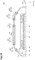
- FIG. 10 illustrates a second variation of the coil device 10.
- a second portion 43f of a conductive pattern 43B is aligned spaced from a first portion 43e along the Z direction.
- the coil device 10B is different from the coil device 10A in that the second portion 43f is provided on the outer surface 22b.
- the second portion 43f may be exposed to rainwater and the like.
- the second portion 43f may be covered from above by a waterproof film.
- the aspect of the coil device 10B according to this variation also achieves the configuration in which the second portion 43f overlaps the first portion 43e in the Z direction, so that the same effects as those of the coil device 10A can be obtained.
- a through hole in the cover 22 for forming a via to electrically connect the first portion 43e to the second portion 43f.
- a through hole penetrating in the Z direction may be formed in the cover 22 at the turn back position RP (see FIG. 8 ) of the conductive pattern 43B, and a via formed of an electrically conductive material may be provided inside the through hole.
- the first portion 43e provided on the inner surface 22a can be electrically connected to the second portion 43f provided on the outer surface 22b by forming such a via.
- the connection wire Cb connected to the second portion 43f is connected to the detection part 52 inside the casing 20, for example, through the through hole formed in the cover 22.
- the detection part 52 is formed outside the casing 20
- a different through hole may be formed in the cover 22 so that the connection wire Ca connected to the first portion 43e is connected to the detection part 52 therethrough.
- the first portion 43e and the second portion 43f may be arranged interchanged with each other. That is, the first portion 43e may be arranged on the outer surface 22b, and the second portion 43f may be arranged on the inner surface 22a.
- FIGS. 11 and 12 illustrate a third variation of the coil device 10.
- a first portion 43g and a second portion 43h of a conductive pattern 43C extend to an edge part of the inner surface 22a closer to the base 21.
- the first portion 43g and the second portion 43h are arranged side by side along the Y direction on the inner surface 22a, and extend along the Z direction toward the base 21.
- the cover 22 is removably attached to the base 21.
- a detection part 52A has a pair of connection parts Cd and Ce.
- Each of the connection parts Cd and Ce is, for example, a spring-like metal terminal projecting from the detection part 52A toward the inner surface 22a.
- the connection parts Cd and Ce contact the first portion 43g and the second portion 43h, respectively, by spring pressure.
- the connection parts Cd and Ce are thus electrically connected to the first portion 43g and the second portion 43h, respectively.
- a contact between the connection part Cd and the first portion 43g is the input part 41, and a contact between the connection part Ce and the second portion 43h is the output part 42.
- the connection parts Cd and Ce are electrically connected to a positive terminal and a negative terminal, respectively, of the detection power source 51.
- connection parts Cd and Ce are electrically connected to the input part 41 and the output part 42, respectively, by the cover 22 being attached to the base 21. Specifically, when the cover 22 is attached to the base 21, the connection parts Cd and Ce contact the first portion 43g and the second portion 43h, respectively. The connection parts Cd and Ce are thus electrically connected to the input part 41 and the output part 42, respectively. When the cover 22 is removed from the base 21, the respective contacts between the connection parts Cd and Ce and the first portion 43g and the second portion 43h are released. The connection parts Cd and Ce are thus electrically disconnected from the input part 41 and the output part 42, respectively.
- the cover 22 in which the deformation has occurred may be removed, and a new cover 22 with no deformation may be attached to the base 21.
- the pair of connection parts Cd and Ce are electrically connected to the input part 41 and the output part 42, respectively, by the cover 22 being attached to the base 21. This facilitates connecting of the detection part 52A to the conductive pattern 43C when attaching a new cover 22 to the base 21.
- FIGS. 13 and 14 illustrate a fourth variation of the coil device 10.
- a coil device 10D according to this variation has a configuration in which the configuration of the coil device 10A illustrated in FIGS. 8 and 9 is combined with the configuration of the coil device 10C illustrated in FIGS. 11 and 12 .
- a first portion 43i, the insulating member F, and a second portion 43j extend to the edge part of the inner surface 22a closer to the base 21.
- an electrical conductor P such as a metal film is interposed between the inner surface 22a and the first portion 43i.
- the electrical conductor P is formed, for example, of a metal material such as copper or aluminum.
- the electrical conductor P is provided in contact with the inner surface 22a.
- the electrical conductor P is also in contact with the first portion 43i, and is electrically connected to the first portion 43i.
- the electrical conductor P extends in the Y direction from a region between the inner surface 22a and the first portion 43i in the X direction.
- the connection part Cd of the detection part 52A is electrically connected to the first portion 43i via the electrical conductor P by the connection part Cd contacting an extended portion of the electrical conductor P.
- the connection part Ce is electrically connected to the second portion 43j by contacting the second portion 43j.
- FIG. 15 illustrates a fifth variation of the coil device 10.
- a conductive part 40E of a coil device 10E includes a crossing portion CP in which a second portion 43m of a conductive pattern 43E three-dimensionally crosses a first portion 43k.
- FIG. 16 illustrates an XZ cross-section of the crossing portion CP. As illustrated in FIG. 16 , the crossing portion CP is arranged side by side with and spaced from the first portion 43k in the Z direction, and crosses the first portion 43k when viewed in the Z direction.
- the crossing portion CP and the first portion 43k may be insulated by being spaced from each other, or by an insulating member such as an insulating sheet being interposed between the crossing portion CP and the first portion 43k.
- the other portions of the second portion 43m other than the crossing portion CP are arranged side by side with the first portion 43k along directions intersecting the Z direction (the X direction and the Y direction in the example illustrated in FIG. 15 ), and extend along the direction of extension of the first portion 43k.
- the first portion 43k and the second portion 43m can be alternately arranged by the second portion 43m including the crossing portion CP.
- the first portion 43k and the second portion 43m are alternately arranged along the X direction.
- a pair of the first portion 43k and the second portion 43m close to each other in the X direction is considered as one set, a plurality of sets (11 sets in FIG. 15 ) are aligned in the X direction.
- an induced voltage is generated as described above.
- the direction of the induced voltage generated in one of two adjacent sets is opposite the direction of the induced voltage generated in the other set, so that the induced voltages generated in these sets are cancelled.
- the entire induced voltage Ei generated between the input part 41 and the output part 42 can be reduced, so that the impact of the induced voltage Ei on the accuracy of electrical resistance measurement of the conductive part 40 by the detection part 52 can be reduced. That is, the likelihood of false detections by the detection part 52 caused by the generation of the induced voltage Ei can be further reduced.
- the crossing portion CP since the first portion 43k and the second portion 43m are aligned spaced apart along the Z direction, the normal direction of the surface region R surrounded by the conductive pattern 43E is substantially at a right angle to the direction of the magnetic field H, similarly to the coil device 10A according to the first variation.
- the induced voltage Ei generated at the crossing portion CP is thus very small.
- the second portion 43m may be closely adhered to the inner surface 22a and the first portion 43k may be arranged side by side with and spaced from the second portion 43m in the Z direction, in a manner that is the opposite of the configuration of the cross-sectional view illustrated in FIG. 16 .
- FIG. 17 illustrates a sixth variation of the coil device 10.
- the coil device 10F includes a plurality of (two in the example illustrated in FIG. 17 ) conductive parts 40F and 40G, and a plurality of (two in the example illustrated in FIG. 17 ) detection parts 52B and 52C.
- a conductive pattern 43F of the conductive part 40F is provided in a region on one side of the cover 22 in the X direction
- a conductive pattern 43G of the conductive part 40G is provided in a region on the other side of the cover 22 in the X direction.
- the input part 41 and the output part 42 of the conductive part 40F are electrically connected to the detection part 52B, and the input part 41 and the output part 42 of the conductive part 40G are electrically connected to the detection part 52C.
- the detection part 52B when deformation occurs in the region on one side of the cover 22 in the X direction, it is detected by the detection part 52B, and when deformation occurs in the region on the other side of the cover 22 in the X direction, it is detected by the detection part 52C.
- the region in which the conductive pattern 43F is provided and the region in which the conductive pattern 43G is provided are divided in the X direction.
- the region in which the conductive pattern 43F is provided and the region in which the conductive pattern 43G is provided may be divided in the Y direction or in any other direction or at any location as long as the conductive pattern 43F and the conductive pattern 43G are provided across the entire region of the cover 22.
- the coil device 10 is applied to the wireless power supply system 1 for charging the battery of a vehicle.
- the coil device may be applied to wireless power supply systems for charging batteries of movable objects other than vehicles, such as underwater vessels.
- the coil device may also be applied to wireless power supply systems for charging batteries of objects other than movable objects, such as consumer electronics, or may be applied to induction heating systems or eddy current flaw detection systems.
- the detection device composed of the conductive part and the detection part may be applied to devices other than the coil device, and may be applied to other devices which have no coils.
- the configuration of the coil device is not limited to the embodiment and the variations above, and may be appropriately changed without departing from the scope of the claims.
- the power transmitting coil is a circular coil
- the power transmitting coil may be other types of coils, such as a solenoid coil in which a conductive wire is helically wound in three-dimensional space.
- the shape, location, and arrangement of the ferrite plate may also be changed according to the type of the coil.
- the conductive pattern 43 includes the portions P1 that extend in the X direction and the portions P2 that extend in the Y direction.
- the directions in which the conductive pattern 43 extend are not limited to those in this example, and may be appropriately changed.
- the conductive pattern 43 may extend in directions oblique to the X direction and the Y direction as long as the entire inner surface 22a is covered, such as in a conductive pattern 43H of a conductive part 40H of a coil device 10H illustrated in FIG. 18 .
- a detection part 52D may have an electric power converter 59 as illustrated in FIG. 19 .
- the electric power converter 59 is provided between the detection power source 51 and the conductive part 40, and is connected to the connection wires Ca and Cb.
- the electric power converter 59 converts the electric power received from the detection power source 51 into electric power suitable for abnormality detection by the conductive part 40.
- the electric power converter 59 may be a DC/DC converter that converts DC power supplied from the detection power source 51 into DC power having a voltage different from the voltage of the first DC power.
- the electric power converter 59 may be a transformer that converts AC power supplied from the detection power source 51 into AC power having a voltage different from the voltage of the first AC power.
- the electric power converter 59 may be an inverter that converts the DC power supplied from the detection power source 51 into AC power having a frequency different from the frequency of the high frequency AC power supplied by the drive power source 30 (that is, a frequency time varying the magnetic field generated by the power transmitting coil C2).
- a conductive pattern 43J of a conductive part 40J may have portions extending in directions intersecting the directions of extension of the fibers as illustrated in FIG. 20.
- FIG. 20 is an enlarged top view of a portion of the conductive pattern 43J.
- the conductive pattern 43J extends in a zigzag manner in the X direction and the Y direction so as to follow the directions perpendicular to the directions of extension of the fibers.
- the directions of cracks in the casing 20 tend to be along the directions of extension of the fibers.
- the base is not limited to a plate-shaped member that ensures the general rigidity of the coil device.
- the cover may have rigidity, if the general rigidity of the coil device is ensured by the combination of the base and the cover, and the function as the coil device can be exhibited.
- a casing 20A may be composed of a combination of a bottomed rectangular tube-shaped base 21A having a depth in the Z direction and a plate-shaped cover 22A.
- the base and the cover may have other shapes. For example, as illustrated in FIG.
- a casing 20B may be composed of a combination of a bottomed rectangular tube-shaped base 21B having a depth less than the depth of the base 21A and a bowl-shaped cover 22B provided so as to close an opening of the base 21B.
Landscapes
- Engineering & Computer Science (AREA)
- Power Engineering (AREA)
- Transportation (AREA)
- Mechanical Engineering (AREA)
- Computer Networks & Wireless Communication (AREA)
- Life Sciences & Earth Sciences (AREA)
- Sustainable Development (AREA)
- Sustainable Energy (AREA)
- Electric Propulsion And Braking For Vehicles (AREA)
- Charge And Discharge Circuits For Batteries Or The Like (AREA)
Abstract
Description
- The present disclosure relates to a coil device, a power supply device, and a detection device.
-
Patent Literatures Patent Literatures Patent Literature 3 discloses a technique capable of detecting that a hole has been formed in a surface of a case which accommodates electrical equipment. The technique disclosed inPatent Literature 3 enables detection of whether a hole has been formed in the case by detecting whether an electrically conductive pattern formed on an inner surface of the case has been cut. -
- Patent Literature 1:
Japanese Unexamined Patent Publication No. 2016-1940 - Patent Literature 2:
Japanese Unexamined Patent Publication No. 2014-197926 - Patent Literature 3:
Japanese Unexamined Patent Publication No. 2000-150685 - For example, when the coil device is used as a charging facility for movable objects such as vehicles or drones, a power receiving side coil device may be installed in the movable object and a power transmitting side coil device may be installed outdoors. When the coil device installed outdoors is exposed to wind and rain, rainwater and the like may intrude into the casing of the coil device and cause performance degradation of the coil device such as reduction in insulating properties of the inside of the casing. It is thus important to ensure the seal of the casing so that rainwater and the like do not intrude into the casing.
- However, when the movable object impacts the coil device, the seal of the casing may be impaired due to the damage to the casing. If the coil device is operated in such a condition in which its performance may be degraded, power transmission or reception by the coil device tend to become unstable.
Patent Literatures Patent Literatures - A coil device according to one aspect of the present disclosure includes a coil generating a magnetic field, a casing accommodating the coil, a conductive part including an input part, an output part, and a conductive pattern connecting the input part to the output part, the conductive part being provided on the casing, and electrically insulated from the casing, and a detection part electrically connected to the input part and the output part, energizing the conductive pattern via the input part and the output part, and detecting deformation in the casing based on an energized state of the conductive pattern.
- The present disclosure provides a coil device, a power supply device, and a detection device which are capable of achieving stable power transmission or reception..
-
-
FIG. 1 is a side view illustrating a wireless power supply system having a coil device according to an embodiment. -
FIG. 2 is a top view illustrating the coil device. -
FIG. 3 is a cross-sectional view taken along line III-III shown inFIG. 2 . -
FIG. 4 is a diagram for describing a surface region surrounded by a conductive pattern. -
FIG. 5 is a diagram illustrating a configuration of a detection part. -
FIG. 6 is an example of a flow chart illustrating a detection method of the detection part. -
FIG. 7 is another example of the flow chart illustrating the detection method of the detection part. -
FIG. 8 is a top view illustrating a first variation of the coil device. -
FIG. 9 is a cross-sectional view taken along line IX-IX shown inFIG. 8 . -
FIG. 10 is a cross-sectional view illustrating a second variation of the coil device. -
FIG. 11 is a cross-sectional view illustrating a third variation of the coil device. -
FIG. 12 is a diagram of an inner surface of a cover seen from the detection part side of the coil device illustrated inFIG. 11 . -
FIG. 13 is a cross-sectional view illustrating a fourth variation of the coil device. -
FIG. 14 is a diagram of the inner surface of the cover seen from the detection part side of the coil device illustrated inFIG. 13 . -
FIG. 15 is a top view illustrating a fifth variation of the coil device. -
FIG. 16 is a cross-sectional view illustrating a crossing portion of the coil device illustrated inFIG. 15 . -
FIG. 17 is a top view illustrating a sixth variation of the coil device. -
FIG. 18 is a top view illustrating a variation of the conductive pattern. -
FIG. 19 is a diagram illustrating a variation of the detection part. -
FIG. 20 is an enlarged top view illustrating another variation of the conductive pattern. -
FIG. 21(a) is a cross-sectional view illustrating a variation of a casing.FIG. 21(b) is a cross-sectional view illustrating another variation of the casing. - A coil device according to one aspect of the present disclosure includes a coil generating a magnetic field, a casing accommodating the coil, a conductive part including an input part, an output part, and a conductive pattern connecting the input part to the output part, the conductive part being provided on the casing, and electrically insulated from the casing, and a detection part electrically connected to the input part and the output part, energizing the conductive pattern via the input part and the output part, and detecting deformation in the casing based on an energized state of the conductive pattern.
- In this coil device, the detection part energizes the conductive pattern of the conductive part provided on the casing. When damage or a break occurs in the conductive pattern in this state, the energized state of the conductive pattern becomes abnormal. For example, when the conductive pattern breaks, no electric current will flow in the conductive pattern, and electrical resistance between the input part and the output part will be infinite. In such a case, it is likely that deformation such as damage or a crack has occurred in the casing. Accordingly, the detection part detects the deformation in the casing on the basis of the energized state of the conductive pattern. When the deformation in the casing can be detected, actions such as stopping the operation of the coil device can be taken. Thus, situations can be suppressed in which the coil device is operated in a state in which deformation has occurred in the casing, that is, in a state in which performance may be degraded. As a result, situations in which power transmission or reception by the coil is unstable can be suppressed.
- In some aspects, the conductive pattern may include a first portion and a second portion arranged side by side on a pattern arrangement surface of the casing. Electric currents in the first portion and in the second portion flow in opposite directions when energized. In this case, an increase in an area of a surface region surrounded by the first portion and the second portion can be suppressed. An induced voltage generated by a magnetic field linking with the surface region is defined by a product of a component of the magnetic field in a normal direction of the surface region and the area of the surface region. An increase in the induced voltage can thus be suppressed by suppressing the increase in the area of the surface region. By suppressing the increase in the induced voltage in this manner, the impact of the induced voltage on the accuracy of detection by the detection part can be suppressed. This reduces the likelihood of false detections by the detection part caused by the generation of the induced voltage.
- In some aspects, the second portion may be arranged side by side with the first portion along a direction intersecting a normal direction of the pattern arrangement surface, and may extend along a direction of extension of the first portion. In this case, the increase in the area of the surface region surrounded by the first portion and the second portion can be effectively suppressed. The increase in the induced voltage can thus be effectively suppressed, and the impact of the induced voltage on the accuracy of detection by the detection part can be effectively suppressed. As a result, the likelihood of false detections by the detection part caused by the generation of the induced voltage can be further reduced.
- In some aspects, the second portion may be arranged side by side with the first portion along a direction intersecting a normal direction of the pattern arrangement surface, and may extend along a direction of extension of the first portion. In this case, the normal direction of the surface region of the conductive pattern surrounded by the first portion and the second portion can be substantially at a right angle to a direction of the magnetic field. The induced voltage generated by the magnetic field linking with the surface region is defined, as described above, by the product of the component of the magnetic field in the normal direction of the surface region and the area of the surface region. Thus, in the case in which the normal direction of the surface region is at a right angle to the direction of the magnetic field, the component of the magnetic field in the normal direction of the surface region is 0, and the induced voltage is also 0. In this configuration, since the normal direction of the surface region can be substantially at a right angle to the direction of the magnetic field, the induced voltage can be closer to 0, and the impact of the induced voltage on the accuracy of detection by the detection part can be minimized. This even further reduces the likelihood of false detections by the detection part caused by the generation of the induced voltage.
- In some aspects, the second portion may include a crossing portion crossing the first portion when viewed in a normal direction of the pattern arrangement surface, and may be arranged side by side with the first portion along the normal direction at the crossing portion. In this case, the impact of the induced voltage on the accuracy of detection by the detection part can be further minimized by the second portion including the crossing portion. That is, the likelihood of false detections by the detection part caused by the generation of the induced voltage can be further reduced.
- In some aspects, the conductive pattern may include a portion extending in one direction of in-plane directions of the pattern arrangement surface, and a portion extending in another of the in-plane directions intersecting the one direction. In this configuration, when damage or cracks occur in the one direction of the pattern arrangement surface, the detection part can detect the deformation in the casing using the portion of the conductive pattern extending in the other direction. When damage or cracks occur in the other direction of the pattern arrangement surface, the detection part can detect the deformation in the casing using the portion of the conductive pattern extending in the one direction. Thus, regardless of whether damage or cracks occur in the one direction or the other direction of the pattern arrangement surface, the detection part can more reliably detect the deformation in the casing on the basis of the energized state of the conductive pattern.
- In some aspects, the pattern arrangement surface may be an inner surface of the casing facing the coil. In this case, situations in which the conductive part degrades due to exposure to rainwater and the like can be avoided. Additionally, since the conductive part is provided on the inner surface of the casing, the conductive part and the detection part can be electrically connected without forming a through hole in the casing. Situations in which the seal of the casing fails can thus be suppressed. As a result, situations in which the coil device is operated in a state in which performance may be degraded can be more reliably suppressed, and situations in which the power transmission or reception by the coil is unstable can be more reliably suppressed.
- In some aspects, the casing may include a cover and a base defining an accommodation space for accommodating the coil. The cover may be removably attached to the base, and the input part and the output part may be provided on the cover. The detection part may include a pair of connection parts provided on the base, and the pair of connection parts may be electrically connected to the input part and the output part, respectively, by the cover being attached to the base. In a case in which deformation occurs in the cover of the casing, the cover in which the deformation has occurred may be removed, and a new cover with no deformation may be attached to the base. In the configuration above, the pair of connection parts of the detection part are electrically connected to the input part and the output part, respectively, of the conductive part by the cover being attached to the base. This facilitates connecting the detection part to the conductive part when attaching a new cover to the base.
- A power supply device according to one aspect of the present disclosure includes any one of the coil devices described above, and a power source part supplying electric power to the coil, wherein the power source part stops supplying electric power to the coil when the detection part detects the deformation in the casing. In this power supply device, situations in which the coil device is operated in a state in which deformation has occurred in the casing, that is, in a state in which performance may be degraded can be more reliably suppressed. Thus, situations in which the power transmission or reception by the coil is unstable can be more reliably suppressed.
- A detection device according to one aspect of the present disclosure detects deformation in a casing of a coil device for wireless power supply, and includes a conductive part including an input part, an output part, and a conductive pattern connecting the input part to the output part, the conductive part being provided on the casing, and electrically insulated from the casing, and a detection part electrically connected to the input part and the output part, energizing the conductive pattern via the input part and the output part, and detecting the deformation in the casing based on an energized state of the conductive pattern.
- In this detection device, the detection part energizes the conductive pattern of the conductive part provided on the casing. When damage or a break occurs in the conductive pattern in this state, the energized state of the conductive pattern becomes abnormal. For example, when the conductive pattern breaks, no electric current will flow in the conductive pattern, and electrical resistance between the input part and the output part will be infinite. In such a case, it is likely that deformation such as damage or a crack has occurred in the casing. Accordingly, the detection part detects the deformation in the casing on the basis of the energized state of the conductive pattern. When the deformation in the casing can be detected, actions such as stopping the operation of the coil device can be taken. Thus, situations can be suppressed in which the coil device is operated in a situation in which deformation has occurred in the casing, that is, in a state in which performance may be degraded. As a result, situations in which the power transmission or reception is unstable can be suppressed.
- Embodiments of the present disclosure will be described in detail below with reference to the accompanying drawings. Like elements are given like reference signs in the description of the drawings and redundant explanation is omitted.
- As shown in
FIG. 1 , acoil device 10 is used, for example, as apower receiving device 11 or apower transmitting device 12 in a wirelesspower supply system 1. The wirelesspower supply system 1, for example, charges a battery installed in a movable object V such as a vehicle or a drone. Thecoil device 10 may be used both as thepower receiving device 11 and thepower transmitting device 12. - When the
coil device 10 is used as thepower transmitting device 12, thecoil device 10 as the power transmittingcoil device 12 is secured, for example, to an outdoor road surface G. Adrive power source 30 of a power source part 5 (seeFIG. 2 ) is connected to a power transmitting coil C2 of thecoil device 10. Thepower source part 5 includes thedrive power source 30, and adetection power source 51 and a control part 53 (seeFIG. 2 ) which are described later. Thepower source part 5 and thecoil device 10 compose apower supply device 2. When thecoil device 10 is used as thepower receiving device 11, thecoil device 10 as thepower receiving device 11 is secured, for example, to a chassis of a vehicle. A power receiving coil C1 of thepower receiving device 11 is connected to a battery via a receiving circuit and a charging circuit, and the like. - When the
power transmitting device 12 and thepower receiving device 11 face each other in an up-down direction, the power transmitting coil C2 and the power receiving coil C1 are electromagnetically coupled to form an electromagnetic coupling circuit. Electric power is thus wirelessly supplied from the power transmitting coil C2 to the power receiving coil C1. In other words, the power receiving coil C1 wirelessly receives electric power from the power transmitting coil C2. The electromagnetic coupling circuit may be a circuit that transmits and receives power by "electromagnetic induction," or a circuit that transmits and receives power by "magnetic resonance." - The
coil device 10 will be described in further detail below with an aspect using thecoil device 10 as thepower transmitting device 12 as an example. In the description below, the up-down direction (for example, vertical direction) in which thepower transmitting device 12 and thepower receiving device 11 face each other is referred to as a Z direction, one direction of in-plane directions perpendicular to the Z direction is referred to as an X direction, and another direction of the in-plane directions perpendicular to the one direction is referred to as a Y direction. - As shown in
FIGS. 2 and3 , thecoil device 10 includes acasing 20, the power transmitting coil C2, aconductive part 40, and adetection part 52. Theconductive part 40 and thedetection part 52 compose adetection device 60. Thecasing 20 is, for example, a flat box-shaped member, and accommodates at least the power transmitting coil C2. As shown inFIG. 3 , thecasing 20 has abase 21 and acover 22 which define an accommodation space for accommodating the power transmitting coil C2. - The
base 21 is a plate-shaped member installed on the road surface G. The base 21 may or may not be secured to the road surface G. The power transmitting coil C2 is provided on thebase 21. The base 21 faces thecover 22 via the power transmitting coil C2 in the Z direction. Thebase 21 ensures the general rigidity of thecoil device 10. The base 21 can be made of various materials such as a resin material or a metal material as long as the general rigidity of thecoil device 10 is ensured. The base 21 may be made to be able to shield magnetic field leakage by making all or a portion of the base 21 from a metal material having low permeability such as aluminum or copper. - The
cover 22 is sealingly attached to the base 21 so as to cover the power transmitting coil C2. The space between the base 21 and thecover 22 is sealed, for example, by an O-ring or a sealing member. Thecover 22 may be removably attached or non-removably secured to thebase 21. The electromagnetic coupling between the power transmitting coil C2 and the power receiving coil C1 is achieved through thecover 22. Thecover 22 is thus formed of a non-magnetic and non-electrically conductive material that does not affect the electromagnetic coupling to enable highly efficient wireless power supply. The non-magnetic and non-electrically conductive material is, for example, a resin material such as glass fiber reinforced plastics (GFRP). Thecover 22 need not be entirely formed of the non-magnetic and non-electrically conductive material. For example, when the electromagnetic coupling between the power transmitting coil C2 and the power receiving coil C1 is achieved through only a portion of thecover 22, only this portion may be formed of the non-magnetic and non-electrically conductive material. In this case, the other portions of thecover 22 other than this portion may be formed of a material that is not non-magnetic and non-electrically conductive. - The
cover 22 has, for example, an opening on a side toward the base 21 in the Z direction, and covers the power transmitting coil C2 on thebase 21. An XZ cross-section of thecover 22 is not limited to a trapezoid shape as shown inFIG. 3 , and may be of other shapes such as rectangular. Thecover 22 includes aninner surface 22a that faces the power transmitting coil C2 side, and anouter surface 22b that faces a side opposite the power transmitting coil C2. Theinner surface 22a and theouter surface 22b compose the surface of thecasing 20. For example, theinner surface 22a and theouter surface 22b each has a portion parallel to an XY plane, and portions inclined relative to the XY plane. The normal directions of theinner surface 22a and theouter surface 22b either match the Z direction or have a Z direction component. Thecover 22 is formed, for example, of a non-electrically conductive material. Thus, theinner surface 22a and theouter surface 22b each forms an insulating surface having electrical insulating properties. - The power transmitting coil C2 is formed, for example, of a
conductive wire 25 spirally wound in the same plane. The power transmitting coil C2 is, for example, a circular coil. In the circular coil, theconductive wire 25 is wound so as to surround the periphery of a winding axis (coil axis). For example, the winding axis extends in the Z direction, and the winding direction of theconductive wire 25 extends spirally in the XY plane. The power transmitting coil C2 generates a magnetic field by being supplied with electric power from thedrive power source 30. Magnetic field lines generated from the power transmitting coil C2 extend toward the power receiving coil C1 and link with the power receiving coil C1. The direction of these magnetic field lines has a Z direction component at thecover 22. The power receiving coil C1 generates an induced current by the magnetic field lines linking with the power receiving coil C1. Thepower receiving device 11 thus wirelessly receives electric power from thepower transmitting device 12. - In the case in which the power transmitting coil C2 is a circular coil, the
conductive wire 25 may be single-layered or multi-layered. The power transmitting coil C2 viewed in the Z direction may have various shapes, such as rectangular, circular, or elliptic. For example, a litz wire in which a plurality of conductor strands insulated from each other are twisted together and high frequency resistance is suppressed by a skin effect or a proximity effect, or a copper or aluminum solid wire may be used as theconductive wire 25. - As shown in
FIG. 3 , the power transmitting coil C2 is, for example, fitted in a groove of abobbin 26 which is a flat plate-shaped member. Thebobbin 26 is formed of a non-magnetic and non-electrically conductive material. For example, silicone or polyphenylene sulfide resin may be usedas the material of thebobbin 26. The position of the power transmitting coil C2 inside thecasing 20 is determined by thebobbin 26 being secured to thebase 21 via acoil holding member 28. Thecoil holding member 28 is hollow, and aferrite plate 27 provided between thebobbin 26 and thebase 21 is held in a hollow section of thecoil holding member 28. Thecoil holding member 28 is formed, for example, of the same material as thebobbin 26. Theferrite plate 27 is, for example, a rectangular flat plate-shaped ferrite core. Theferrite plate 27 is magnetic, and directs and concentrates the magnetic field lines generated from the power transmitting coil C2. - The
drive power source 30 is electrically connected to the power transmitting coil C2. Thedrive power source 30 supplies electric power, which is necessary to wirelessly supply power to the movable object V, to the power transmitting coil C2. Thedrive power source 30, for example, receives single phase AC power such as commercial AC power, and converts the single phase AC power into DC power by a rectifier circuit and a smoothing circuit. Thedrive power source 30 then converts the DC power into high frequency AC power by an inverter circuit, and supplies the high frequency AC power to the power transmitting coil C2. The magnetic field generated from the power transmitting coil C2 with this high frequency AC power is a sinusoidally time-varying AC magnetic field. The high frequency AC power has a frequency of, for example, about 100 kHz, but not limited to this. The high frequency AC power may have a frequency of lower than 100 kHz (for example, 10 kHz), or a frequency of higher than 100 kHz (for example, a few MHz). - The
conductive part 40 is provided on thecasing 20, and is electrically insulated from thecasing 20. Theconductive part 40 being electrically insulated from thecasing 20 includes both a case in which at least a portion of thecasing 20 on which theconductive part 40 is provided is an insulator, and a case in which an insulating member such as an insulating sheet is interposed between thecasing 20 and theconductive part 40. In the case in which an insulating member is interposed between thecasing 20 and theconductive part 40, the insulating member may be provided on thecasing 20 or theconductive part 40. - The
conductive part 40 is provided, for example, on theinner surface 22a of thecover 22 of thecasing 20. A portion of theconductive part 40 may extend to an edge part of theinner surface 22a closer to thebase 21. Theconductive part 40 may be either directly provided on theinner surface 22a, or indirectly provided on theinner surface 22a via another member. The position at which theconductive part 40 is provided on thecasing 20 is not limited. - As illustrated in
FIGS. 2 and3 , theconductive part 40 has aninput part 41, anoutput part 42, and aconductive pattern 43. Theinput part 41 and theoutput part 42 are portions that are electrically connected to thedetection part 52 described later. Theconductive pattern 43 is a linear wiring pattern that continues from theinput part 41 to theoutput part 42. Theconductive pattern 43 is formed, for example, of an electrically conductive material such as copper or aluminum. Theconductive pattern 43 and thedetection part 52 form an electrical closed circuit. Theconductive pattern 43 may be formed on theinner surface 22a by methods such as deposition or adhesion. In the case in which theconductive pattern 43 is formed on theinner surface 22a by methods such as deposition or adhesion, theconductive pattern 43 can be closely adhered to theinner surface 22a. Thus, when deformation such as fractures or fissures (cracks) occur in thecover 22, cracks or breaks also tend to occur in theconductive pattern 43. Theconductive pattern 43 extends so as to meander across theinner surface 22a in a predetermined direction. Theconductive pattern 43 which extends from theinput part 41 turns back at a predetermined position (turn back position RP) of theinner surface 22a, and reaches theoutput part 42. Theinner surface 22a is a pattern arrangement surface on which theconductive pattern 43 is arranged. In a case in which theconductive pattern 43 is arranged on theouter surface 22b, theouter surface 22b is the pattern arrangement surface. In a case in which theconductive pattern 43 is arranged on both theinner surface 22a and theouter surface 22b, both theinner surface 22a and theouter surface 22b are the pattern arrangement surfaces. - The
conductive pattern 43 includes afirst portion 43a that is connected to theinput part 41, and asecond portion 43b that is connected to theoutput part 42. Thefirst portion 43a and thesecond portion 43b are close to each other. Thefirst portion 43a and thesecond portion 43b are arranged side by side, spaced apart by a distance necessary for electrical insulation. Thefirst portion 43a extends from theinput part 41 to the turn back position RP. Thesecond portion 43b extends from the turn back position RP to theoutput part 42 so as to trace backwards the same path as the path of thefirst portion 43a from theinput part 41 to the turn back position RP, spaced apart from thefirst portion 43a by a spacing distance. Thus, when energized, in the portions in which thesecond portion 43b and thefirst portion 43a are close to each other, the electric current in thesecond portion 43b flows in the direction opposite the direction in which the electric current in thefirst portion 43a flows. Thefirst portion 43a and thesecond portion 43b are connected to each other via anotherportion 43x of theconductive pattern 43 positioned at the turn back position RP. A width of thesecond portion 43b in a width direction (that is, a direction perpendicular to a direction of extension) may be the same as a width of thefirst portion 43a in the width direction, or may be different from the width of thefirst portion 43a. - The path along which the
conductive pattern 43 including thefirst portion 43a and thesecond portion 43b extends meanders such that theconductive pattern 43 is present across the entireinner surface 22a. When deformation occurs in an arbitrary position of thecover 22 and theconductive pattern 43 passes through that position, a break or the like may occur in theconductive pattern 43 due to the deformation in thecover 22. In the example illustrated inFIG. 2 , theconductive pattern 43 includes portions P1 that extend along the X direction, and portions P2 that extend along the Y direction. The portions P1 that extend along the X direction and the portions P2 that extend along the Y direction are alternately connected. - As illustrated in
FIG. 4 , a distance W between thefirst portion 43a and thesecond portion 43b is minimized to the extent that electrical insulation between thefirst portion 43a and thesecond portion 43b can be secured. Thus, an area A of a surface region R surrounded by theconductive pattern 43 can be minimized. When the high frequency AC power is supplied to the power transmitting coil C2 for wireless power supply, and the magnetic field lines generated from the power transmitting coil C2 link with the surface region R, an induced voltage is generated between theinput part 41 and theoutput part 42. The induced voltage is defined by a product of the area A of the surface region R and a component of the magnetic field in a normal direction of the surface region R. The component of the magnetic field in the normal direction of the surface region R is a resolved component being the magnitude (intensity) of the magnetic field resolved in the normal direction. The area A of the surface region R is, as illustrated inFIG. 4 , defined by a product of a length L of thefirst portion 43a or thesecond portion 43b in the direction of extension and the distance W between thefirst portion 43a and thesecond portion 43b in the direction perpendicular to the direction of extension. - Assuming that the magnetic field generated from the power transmitting coil C2 is a spatially homogeneous magnetic field sinusoidally time-varying at a frequency f, this magnetic field H is represented by formula (1) below. In formula (1), C is a constant, and t is time. The component of the magnetic field H in the normal direction of the surface region R is represented by H sin θ, where θ is an angle between the surface region R and the direction of the magnetic field H. Thus, an induced current Ei is represented by a product of the area A of the surface region R and the component H sin θ of the magnetic field H in the normal direction of the surface region R, as per formula (2) below. In this embodiment, the surface region R surrounded by the
first portion 43a and thesecond portion 43b lies along the XY plane, and the direction of the magnetic field H is generally along the Z direction. Thus, the direction of the magnetic field H is at a right angle to (θ = 90°) or at an angle close to a right angle to the surface region R. In such a case in which the direction of the magnetic field H is perpendicular to the surface region R, that is, in the case in which the direction of the magnetic field H is along the normal direction of the surface region R, the induced voltage Ei is defined by a product of the area A of the surface region R and the magnetic field H. On the other hand, in a case in which the direction of the magnetic field H is along the surface region R (θ= 0°), that is, in the case in which the direction of the magnetic field H is at a right angle to the normal direction of the surface region R, the induced voltage Ei is 0.
[Formula 1]

- When the induced voltage Ei defined as above is high, the
detection part 52 may make false detections as described later. It is thus preferable to adjust the induced voltage Ei to be minimized. To reduce the induced voltage Ei, the area A of the surface region R is reduced, as shown in formula (2). Consequently, arranging theconductive pattern 43 on theinner surface 22a such that the area A of the surface region R is small can reduce the likelihood of thedetection part 52 making false detections. - To reduce the area A of the surface region R, the length L of the
first portion 43a and thesecond portion 43b in the direction of extension is reduced, and the distance W between thefirst portion 43a and thesecond portion 43b is reduced. However, reducing the length L of thefirst portion 43a and thesecond portion 43b in the direction of extension will make it difficult to extend theconductive pattern 43 across a large area of theinner surface 22a. In this case, deformation in thecover 22 may not be detected when the deformation occurs in a portion of thecover 22 across which theconductive pattern 43 does not extend, since no breaks or the like will occur in theconductive pattern 43. Thus, in this embodiment, the area A of the surface region R is reduced by minimizing the distance W between thefirst portion 43a and thesecond portion 43b. - The
detection part 52 is electrically connected to theconductive part 40. Thedetection part 52 utilizes theconductive part 40 to detect deformation that occurs in thecasing 20. As illustrated inFIG. 5 , A pair of connection wires Ca and Cb connected to thedetection part 52. The connection wire Ca connects a positive terminal of thedetection part 52 to theinput part 41. The connection wire Cb connects a negative terminal of thedetection part 52 to theoutput part 42. - The
detection power source 51 of thepower source part 5 supplies electric power to thedetection part 52 according to instructions from thecontrol part 53 of thepower source part 5. When electric power is supplied from thedetection power source 51, electric current flows in theconductive pattern 43 and a voltage is generated between theinput part 41 and theoutput part 42. The electric power may be either direct current or alternating current. When thedetection power source 51 is an AC power source, a frequency f1 and a modulation frequency f2 are set so that they are very different from each other, where f1 is the frequency of the AC power source, and f2 is the modulation frequency of the magnetic field that wirelessly supplies power from the power transmitting coil C2 to the power receiving coil C1. Additionally, a filter which has a frequency selectivity that passes a signal of the frequency f1 and prevents the passing of a signal of the modulation frequency f2 is provided in thedetection part 52. Accordingly, the impact of the magnetic field that wirelessly supplies power from the power transmitting coil C2 to the power receiving coil C1 on the detection of deformation in thecasing 20 based on an energized state of theconductive pattern 43 can be reduced. - The
detection power source 51 may be provided inside or outside thecasing 20. In the case in which thedetection power source 51 is provided outside thecasing 20, thedetection power source 51 may be positioned close to or away from thecasing 20. Thedetection part 52 is protected from rainwater and the like outside thecasing 20 by being provided inside thecasing 20. It would also be unnecessary to pass the connection wire Ca and the connection wire Cb through thecasing 20. However, thedetection part 52 may be provided outside thecasing 20, with the connection wire Ca and the connection wire Cb made to pass through thecasing 20. Similarly, thecontrol part 53 may be provided inside or outside thecasing 20. In the case in which thecontrol part 53 is provided outside thecasing 20, thecontrol part 53 may be positioned close to or away from thecasing 20. - The
detection part 52 is provided, for example, on thebase 21, and is operated by electric power being supplied from thedetection power source 51. Thedetection part 52 is electrically connected to one end of each of the pair of connection wires Ca and Cb. Thedetection part 52 detects deformation that occurs in thecasing 20 on the basis of the energized state of theconductive pattern 43. An "energized state" of theconductive pattern 43 is the electrical resistance between theinput part 41 and theoutput part 42 to which theconductive pattern 43 is connected. "Deformation" of thecasing 20 includes cracks, fractures, damage, or the like that occurs in thecasing 20 that may form a path through which fluid such as water or oil, or gas such as corrosive gas intrudes into thecasing 20 from outside. - The
detection part 52 includes ameasurement part 55, adetermination part 57, and a stabilizedpower source 58. The stabilizedpower source 58 is provided to operate themeasurement part 55 and thedetermination part 57. The stabilizedpower source 58 supplies electric power of a constant voltage to themeasurement part 55 and thedetermination part 57. Themeasurement part 55 includes, for example, acurrent meter 55a, avoltage meter 55b, and acalculation part 56. Thecurrent meter 55a measures a current value flowing in theconductive pattern 43 between theinput part 41 and theoutput part 42. Thevoltage meter 55b measures a voltage value between theinput part 41 and theoutput part 42. The measured current value and voltage value are output to thecalculation part 56. In the example illustrated inFIG. 5 , themeasurement part 55 is composed of thecurrent meter 55a and thevoltage meter 55b, but the configuration of themeasurement part 55 is not limited to the example illustrated inFIG. 5 , and may vary as appropriate. - The
current meter 55a measures the current value (Im) that flows through theconductive part 40. Thevoltage meter 55b is connected to the connection wire Ca connected to theinput part 41 and the connection wire Cb connected to theoutput part 42, and measures the voltage value (Vm) between theinput part 41 and theoutput part 42. Thecalculation part 56 calculates a value obtained by dividing the voltage value Vm by the current value Im, that is, the value of Vm/Im, and outputs the value of Vm/Im to thedetermination part 57. The value of Vm/Im is equal to the electrical resistance between theinput part 41 and theoutput part 42. An example of thecurrent meter 55a includes a current meter that measures the magnetic field generated along with the electric current using a Hall element. An example of thevoltage meter 55b includes a voltage meter that measures using an A/D converter. - The
conductive part 40 is electrically insulated from thecasing 20, and thefirst portion 43a and thesecond portion 43b are electrically insulated from each other. Thus, when thedetection power source 51 applies a voltage between theinput part 41 and theoutput part 42, an electric current flows along a path of entering from theinput part 41, flowing along thefirst portion 43a, passing the turn back position RP, returning along thesecond portion 43b, and exiting from theoutput part 42. Consequently, short-circuiting between thefirst portion 43a and thesecond portion 43b does not occur. That is, a short circuit current does not flow between thefirst portion 43a and thesecond portion 43b. As such, the electrical resistance of theconductive pattern 43 can be measured by thecurrent meter 55a measuring the current value Im that flows in theconductive pattern 43, and thecalculation part 56 calculating the value of Vm/Im. - The
determination part 57 is composed of a computer including, for example, hardware such as a central processing unit (CPU), a read only memory (ROM), and a random access memory (RAM), and software such as a program stored in the ROM. Thedetermination part 57 determines whether deformation has occurred in thecasing 20 by determining whether the energized state of theconductive pattern 43 is abnormal by the electrical resistance output from thecalculation part 56. Thedetermination part 57 determines whether the energized state of theconductive pattern 43 is abnormal, for example, by comparing the electrical resistance to a preset threshold. This threshold is reference electrical resistance for determining the energized state of theconductive pattern 43. When the electrical resistance exceeds the threshold, thedetermination part 57 determines that the energized state of theconductive pattern 43 is abnormal. When the electrical resistance does not exceed the threshold, thedetermination part 57 determines that the energized state of theconductive pattern 43 is not abnormal. - For example, when the
conductive pattern 43 breaks, no electric current flows in theconductive pattern 43, so that the electrical resistance becomes infinite and exceeds the threshold. The electrical resistance may also exceed the threshold in a case in which theconductive pattern 43 is damaged without breaking. The case in which theconductive pattern 43 is damaged without breaking refers is, for example, a case in which a portion of theconductive pattern 43 is torn, a case in which theconductive pattern 43 is stretched and thinned, or the like. In such cases, the cross-sectional area of a damaged portion of theconductive pattern 43 perpendicular to the direction of extension of theconductive pattern 43 is reduced. Accordingly, the electrical resistance may increase and exceed the threshold. - When the electrical resistance exceeds the threshold, the
determination part 57 determines that the energized state of theconductive pattern 43 is abnormal, and determines that damage, a break, or the like has occurred in theconductive pattern 43. Since theconductive pattern 43 is formed closely adhered to theinner surface 22a, it can be assumed that the damage, break, or the like in theconductive pattern 43 has occurred due to deformation in thecover 22. Thus, when the electrical resistance exceeds the threshold, thedetermination part 57 determines that deformation has occurred in thecasing 20, and outputs a detection signal D1 indicating that deformation has occurred in thecasing 20 to thecontrol part 53. When the electrical resistance does not exceed the threshold, thedetermination part 57 determines that the energized state of theconductive pattern 43 is not abnormal, and determines that no damage, breaks, or the like have occurred in theconductive pattern 43. In this case, thedetermination part 57 determines that no deformation has occurred in thecasing 20. - In a case in which detection by the
detection part 52 is performed while the power transmitting coil C2 is transmitting power, the induced voltage Ei generated by the magnetic field lines linking with the surface region R is applied between theinput part 41 and theoutput part 42, in addition to the voltage from thedetection power source 51. In this case, the voltage value measured by thevoltage meter 55b is a value obtained by adding the induced voltage Ei to a voltage Es applied from thedetection power source 51, or by subtracting the induced voltage Ei from the voltage Es. The measured electrical resistance is thus offset by (1±Ei/Es) times compared to a case in which the power transmitting coil C2 is not transmitting power. Consequently, when the induced voltage Ei increases, it is difficult for thedetermination part 57 to accurately compare the electrical resistance according to the voltage applied from thedetection power source 51 to the threshold. Thus, as described above, by arranging theconductive pattern 43 on theinner surface 22a so that the area A of the surface region R is small, the induced voltage Ei can be reduced. This reduces the impact of the induced voltage Ei on the determination accuracy of thedetermination part 57, and reduces the likelihood of false detections by thedetection part 52. - Rt is threshold electrical resistance, and Rn is the electrical resistance of the
conductive part 40 when no deformation has occurred in thecasing 20. It is assumed that, when no deformation has occurred in thecasing 20, the measured values of the electrical resistance of theconductive part 40 detected by thedetection part 52 vary in a range of (Rn-N1) to (Rn+N2) by being affected by the induced voltage Ei when power is transmitted by transmitting coil C2. N1 and N2 indicate error components of the electrical resistance caused by periodic variation of the induced voltage. In this case, in order to satisfy (Rn+N2) < Rt, the induced voltage Ei may be reduced so that N2 is reduced. To achieve this, theconductive pattern 43 may be arranged on theinner surface 22a such that the induced voltage Ei is small. N1 and N2 depend, not only on the induced voltage Ei, but also on the circuit structure of thedetection part 52. However, once the circuit structure of thedetection part 52 is determined, N1 and N2 can be reduced by reducing the induced voltage Ei. - The
control part 53 is composed of a computer including, for example, hardware such as a CPU, a ROM, and a RAM, and software such as a program stored in the ROM. Thecontrol part 53 controls operations of thedetection power source 51 and thedrive power source 30, and issues a warning to anadministrator 100 who manages the operation state of thecoil device 10. Thecontrol part 53 is electrically connected to thedetection power source 51 and thedrive power source 30, and is capable of transmitting and receiving control signals to and from thedetection power source 51 and thedrive power source 30. Thecontrol part 53 may be connected to thedetection power source 51 and thedrive power source 30 so as to be able to transmit and receive the control signals using a wired, wireless, network communication system, or the like. Thecontrol part 53 outputs a control signal D2 to thedetection power source 51 to instruct starting or stopping of the power supply from thedetection power source 51. - The
control part 53 also outputs a control signal D4 to thedetection power source 51 to instruct starting or stopping of the power supply from thedrive power source 30. Upon receiving the detection signal D1 from thedetermination part 57, thecontrol part 53 issues a warning D3 to theadministrator 100 and outputs the control signal D4 to thedrive power source 30 to instruct stopping of the power supply to the power transmitting coil C2. Thecontrol part 53 issuing the warning D3 to theadministrator 100 upon receiving the detection signal D1 thus enables theadministrator 100 to know that deformation has occurred in thecasing 20 early on. Accordingly, theadministrator 100 is capable of responding quickly such as by replacing thecover 22 or thecoil device 10. - When the
control part 53 receives the detection signal D1, thecontrol part 53 may perform only one of issuing the warning D3 to theadministrator 100, or outputting the control signal D4 to thedrive power source 30 to instruct stopping of the power supply to the power transmitting coil C2. In a case in which a plurality of thecoil devices 10 is used for the wirelesspower supply system 1, thecontrol part 53 may issue warnings having identification (ID) numbers to theadministrator 100 to identify thecoil devices 10. This enables theadministrator 100 to recognize from whichcoil device 10 the warning was issued. - A detection method by the
detection part 52 will now be described with reference toFIGS. 6 and7 . The example illustrated inFIG. 6 mainly considers the situation in which detection by thedetection part 52 is performed while power is being supplied to the power transmitting coil C2. The example illustrated inFIG. 7 considers the situation in which detection by thedetection part 52 is performed before power is supplied to the power transmitting coil C2. The example illustrated inFIG. 6 is described first. - As illustrated in
FIG. 6 , thedetection power source 51 supplies electric power to thedetection part 52 according to the control signal D2 (step S1). Theconductive pattern 43 is thus energized. Thedetermination part 57 then determines whether there is deformation in thecasing 20 on the basis of the energized state of the conductive pattern 43 (step S2). Specifically, themeasurement part 55 measures the electrical resistance between theinput part 41 and theoutput part 42, and thedetermination part 57 determines whether that electrical resistance exceeds the threshold. If thedetermination part 57 determines that the electrical resistance does not exceed the threshold, thedetermination part 57 determines that no deformation has occurred in the casing 20 (No in step S2). In this case, steps S1 and S2 are repeated. - If the
determination part 57 determines that the electrical resistance exceeds the threshold, thedetermination part 57 determines that deformation has occurred in the casing 20 (Yes in step S2). In this case, thedetermination part 57 outputs the detection signal D1 indicating that deformation has occurred in thecasing 20 to thecontrol part 53. Upon receiving the detection signal D1, thecontrol part 53 issues the warning D3 to the administrator 100 (step S3). Thecontrol part 53 then checks whether thedrive power source 30 is supplying electric power to the power transmitting coil C2 (step S4). If thedrive power source 30 is not supplying electric power to the power transmitting coil C2 (No in step S4), steps S1, S2, S3, and S4 are repeated. If, however, thedrive power source 30 is supplying electric power to the power transmitting coil C2 (Yes in step S4), thecontrol part 53 outputs the control signal D4 to thedrive power source 30 to instruct stopping of the power supply to the power transmitting coil C2, and thedrive power source 30 stops the power supply to the power transmitting coil C2 upon receiving the control signal D4 (step S5). - The example illustrated in
FIG. 7 is described next. In this example, thecontrol part 53 checks whether thedrive power source 30 will start the power supply to the power transmitting coil C2 (step S11). If thedrive power source 30 will not start the power supply to the power transmitting coil C2 (No in step S11), step S11 is repeated. If, however, thedrive power source 30 is about to start the power supply to the power transmitting coil C2 (Yes in step S11), thecontrol part 53 outputs the control signal D2 to thedetection power source 51 to instruct starting of the power supply to thedetection part 52. Thedetection power source 51 starts the power supply to thedetection part 52 upon receiving the control signal D2 (step S12). Theconductive pattern 43 is thus energized. - The
determination part 57 then determines whether deformation has occurred in thecasing 20 on the basis of the energized state of the conductive pattern 43 (step S13). Specifically, themeasurement part 55 measures the electrical resistance between theinput part 41 and theoutput part 42, and thedetermination part 57 determines whether that electrical resistance exceeds the threshold. If thedetermination part 57 determines that the electrical resistance does not exceed the threshold, thedetermination part 57 determines that no deformation has occurred in the casing 20 (No in step S13). In this case, thecontrol part 53 outputs the control signal D2 to thedetection power source 51 to instruct stopping of the power supply to thedetection part 52. Thedetection power source 51 stops the power supply to thedetection part 52 upon receiving the control signal D2 (step S15). - The
control part 53 then outputs the control signal D4 to thedrive power source 30 to start the power supply to the power transmitting coil C2, and thedrive power source 30 starts the power supply to the power transmitting coil C2 upon receiving the control signal D4 (step S16). When an event occurs indicating that the power supply should be stopped, such as when the battery of the vehicle is fully charged or when a predetermined charging time has passed, thecontrol part 53 outputs the control signal D4 to thedrive power source 30 to stop the power supply to the power transmitting coil C2. Thedetection power source 30 stops the power supply to the power transmitting coil C2 upon receiving the control signal D4 (step S17). If, however, thedetermination part 57 determines that the electrical resistance exceeds the threshold, thedetermination part 57 determines that deformation has occurred in the casing 20 (Yes in step S13). In this case, thedetermination part 57 outputs the detection signal D1 indicating that deformation has occurred in thecasing 20 to thecontrol part 53. Upon receiving the detection signal D1, thecontrol part 53 issues the warning D3 to theadministrator 100. Thecontrol part 53 also outputs the control signal D2 to thedetection power source 51 to instruct stopping of the power supply to thedetection part 52. Upon receiving the control signal D2, thedetection power source 51 stops the power supply to the detection part 52 (step S14). The process returns to step S11 without starting the power supply to the power transmitting coil C2. In the example illustrated inFIG. 7 , the detection by thedetection part 52 is performed before starting the power supply to the power transmitting coil C2, so that it is unnecessary to continually supply power from thedetection power source 51 to thedetection part 52 to perform the detection by thedetection part 52. Power consumption required to supply power from thedetection power source 51 to thedetection part 52 can thus be reduced. - The operation and effects obtained by the
coil device 10 and thedetection device 60 described above will be described. In thecoil device 10 and thedetection device 60, thedetection part 52 energizes theconductive pattern 43 of theconductive part 40 provided on thecasing 20. When damage or a break occurs in theconductive pattern 43 in this state, the energized state of theconductive pattern 43 becomes abnormal. For example, when theconductive pattern 43 breaks, no electric current will flow in theconductive pattern 43, and the electrical resistance between theinput part 41 and theoutput part 42 will be infinite. Alternatively, when theconductive pattern 43 is stretched and thinned, the electrical resistance between theinput part 41 and theoutput part 42 will increase. In such cases, since thecasing 20 and theconductive pattern 43 are closely adhered, deformation in thecasing 20 and a break in theconductive pattern 43 will occur at the same time, and thus it is likely that deformation such as damage or a crack has occurred in thecasing 20. Accordingly, thedetection part 52 detects the deformation in thecasing 20 on the basis of the energized state of theconductive pattern 43. That is, thedetection part 52 detects whether deformation has occurred in thecasing 20 by detecting the electrical resistance between theinput part 41 and theoutput part 42. If deformation in thecasing 20 can be detected, actions such as stopping the operation of thecoil device 10 can be taken. Thus, situations in which thecoil device 10 is operated in a state in which deformation has occurred in thecasing 20, that is, in a state in which performance may be degraded can be suppressed. As a result, situations in which the power transmission by the power transmitting coil C2 is unstable can be suppressed. - The
conductive pattern 43 extends so as to meander across the entireinner surface 22a. Thus, no matter what position the deformation occurs in thecover 22, theconductive pattern 43 will be present in that position, so that damage or breaks in theconductive pattern 43 will more reliably occur with the deformation in thecover 22. As a result, the detection of the deformation in thecover 22 based on the energized state of theconductive pattern 43 can be more reliably performed. That is, situations in which the deformation in thecover 22 fails to be detected by relying on the position at which the deformation occurs in thecover 22 can be suppressed. - The
conductive part 40 is electrically insulated from thecasing 20, and thefirst portion 43a and thesecond portion 43b are electrically insulated from each other. Thus, when electric power is supplied between theinput part 41 and theoutput part 42, electric current flows along the direction of extension of theconductive pattern 43. That is, a short circuit current does not flow between thefirst portion 43a and thesecond portion 43b. Consequently, the electrical resistance of theconductive pattern 43 can be correctly measured by thevoltage meter 55b measuring the voltage value Vm between theinput part 41 and theoutput part 42, thecurrent meter 55a measuring the current value Im that flows in theconductive pattern 43, and thecalculation part 56 calculating the value of Vm/Im. - In the
coil device 10, theconductive pattern 43 includes thefirst portion 43a and thesecond portion 43b arranged side by side on theinner surface 22a, and the electric currents in thefirst portion 43a and in thesecond portion 43b flow in opposite directions when energized. This configuration enables an increase in the area A of the surface region R surrounded by thefirst portion 43a and thesecond portion 43b to be suppressed. As described above, the induced voltage Ei generated by the magnetic field linking with the surface region R is defined by the product of the component of the magnetic field in the normal direction of the surface region R and the area A of the surface region R. An increase in the induced voltage Ei can thus be suppressed by suppressing the increase in the area A of the surface region R. By suppressing the increase in the induced voltage Ei in this manner, the impact of the induced voltage Ei on the accuracy of electrical resistance measurement of theconductive part 40 by thedetection part 52 can be suppressed. This reduces the likelihood of false detections by thedetection part 52 caused by the generation of the induced voltage Ei. Although a magnetic field that electromagnetically couples the power transmitting coil C2 and the power receiving coil C1 is generated with the wireless power supply, the likelihood of false detections by thedetection part 52 can also be reduced during the wireless power supply. - In the
coil device 10, thesecond portion 43b of theconductive pattern 43 is arranged side by side with thefirst portion 43a along directions intersecting the normal direction of theinner surface 22a (that is, the X direction and the Y direction), and extends along the direction of extension of thefirst portion 43a. This configuration enables the increase in the area A of the surface region R of theconductive pattern 43 surrounded by thefirst portion 43a and thesecond portion 43b to be effectively suppressed. Accordingly, the increase in the induced voltage Ei can be effectively suppressed. By suppressing the increase in the induced voltage Ei in this manner, the impact of the induced voltage Ei on the accuracy of electrical resistance measurement of theconductive part 40 by thedetection part 52 can be effectively suppressed. This further reduces the likelihood of false detections by thedetection part 52 caused by the generation of the induced voltage Ei. - In the
coil device 10, theconductive pattern 43 includes portions P1 that extend along the X direction, and portions P2 that extend along the Y direction. This configuration enables thedetection part 52 to detect the deformation in thecasing 20 using the portions P1 of theconductive pattern 43 when damage or cracks occur on theinner surface 22a in the Y direction. When damage or cracks occur on theinner surface 22a in the X direction, thedetection part 52 can detect the deformation in thecasing 20 using the portions P2 of theconductive pattern 43. Thedetection part 52 can thus more reliably detect the deformation in thecasing 20 on the basis of the energized state of theconductive pattern 43 regardless of whether the damage or cracks occur on theinner surface 22a in the X direction or the Y direction. - In the
coil device 10, theconductive part 40 is provided on theinner surface 22a of thecover 22. Thus, situations in which theconductive part 40 degrades due to exposure to rainwater and the like can be avoided. Additionally, since theconductive part 40 is provided on theinner surface 22a of thecasing 20, by providing thedetection part 52 inside thecasing 20, theconductive part 40 and thedetection part 52 can be electrically connected without forming a through hole in thecasing 20. Situations in which the seal of thecasing 20 fails can thus be suppressed. As a result, situations in which thecoil device 10 is operated in a state in which performance may be degraded can be more reliably suppressed, and situations in which the power transmission by the power transmitting coil C2 is unstable can be more reliably suppressed. - In the
power supply device 2, thecontrol part 53 of thepower source part 5 stops the power supply to the power transmitting coil C2 when thedetection part 52 detects deformation. According to this configuration, situations in which thecoil device 10 is operated in a state in which deformation has occurred in thecasing 20, that is, in a state in which performance may be degraded can be more reliably suppressed. Thus, situations in which the power transmission by the power transmitting coil C2 is unstable can be more reliably suppressed. - Although one embodiment of the present disclosure has been described above, the present disclosure is not limited thereto.
FIGS. 8 and9 illustrate a first variation of thecoil device 10. The difference between acoil device 10A according to this variation and thecoil device 10 according to the embodiment above is the arrangement relation of the first portion and the second portion of the conductive pattern. In aconductive part 40A of thecoil device 10A, asecond portion 43d of aconductive pattern 43A is arranged side by side with and spaced apart from afirst portion 43c along the Z direction, and extends so as to overlap thefirst portion 43c when viewed in the Z direction. - The
second portion 43d is arranged on a side of thefirst portion 43c closer to the power transmitting coil C2 in the Z direction. An insulating member F such as an insulating film is interposed between thefirst portion 43c and thesecond portion 43d. Thefirst portion 43c and thesecond portion 43d are electrically insulated by the insulating member F. In such a case in which thefirst portion 43c and thesecond portion 43d are arranged overlapping each other in the Z direction, the normal direction of the surface region R (seeFIG. 4 ) surrounded by theconductive pattern 43A is perpendicular to the direction of extension of the magnetic field lines. - The induced current Ei generated between the
input part 41 and theoutput part 42 by the magnetic field lines linking with the surface region R is defined as the product of the area A of the surface region R and the component H sin θ of the magnetic field H in the normal direction of the surface region R. Thus, in the case in which the normal direction of the surface region R is perpendicular to the direction of extension of the magnetic field lines, the component H sin θ of the magnetic field H in the normal direction of the surface region R is 0, and the induced voltage Ei is also 0. The configuration of thecoil device 10A enables the normal direction of the surface region R surrounded by theconductive pattern 43A to be substantially at a right angle to the direction of the magnetic field H, so that the induced voltage Ei can be closer to 0. Thecoil device 10A thus even further reduces the likelihood of false detections by thedetection part 52 caused by the generation of the induced voltage Ei. Additionally, thefirst portion 43c is closely adhered to thecasing 20. Consequently, similarly to thecoil device 10, when deformation occurs in thecasing 20, a break will also occur in thefirst portion 43c, so that the deformation in thecasing 20 can be detected from a conductive state of theconductive pattern 43A. Thefirst portion 43c and thesecond portion 43d may be arranged interchanged with each other. In this case, thesecond portion 43d will be closely adhered to the casing 20 (specifically, theinner surface 22a of the cover 22), and thefirst portion 43c will be arranged on a side of thesecond portion 43d closer to the power transmitting coil C2 in the Z direction. AlthoughFIG. 9 illustrates an example in which the thickness of the insulating member F is uniform, the thickness of the insulating member F may vary by location as long as thefirst portion 43c and thesecond portion 43d are electrically insulated. -
FIG. 10 illustrates a second variation of thecoil device 10. In acoil device 10B according to this variation, similarly to thecoil device 10A, asecond portion 43f of aconductive pattern 43B is aligned spaced from afirst portion 43e along the Z direction. However, thecoil device 10B is different from thecoil device 10A in that thesecond portion 43f is provided on theouter surface 22b. As illustrated inFIG. 10 , in the case in which thesecond portion 43f is provided on theouter surface 22b, thesecond portion 43f may be exposed to rainwater and the like. Thus, to suppress the degradation of thesecond portion 43f due to contact with rainwater and the like, thesecond portion 43f may be covered from above by a waterproof film. The aspect of thecoil device 10B according to this variation also achieves the configuration in which thesecond portion 43f overlaps thefirst portion 43e in the Z direction, so that the same effects as those of thecoil device 10A can be obtained. - In the
coil device 10B, it is necessary to form a through hole in thecover 22 for forming a via to electrically connect thefirst portion 43e to thesecond portion 43f. For example, a through hole penetrating in the Z direction may be formed in thecover 22 at the turn back position RP (seeFIG. 8 ) of theconductive pattern 43B, and a via formed of an electrically conductive material may be provided inside the through hole. Thefirst portion 43e provided on theinner surface 22a can be electrically connected to thesecond portion 43f provided on theouter surface 22b by forming such a via. The connection wire Cb connected to thesecond portion 43f is connected to thedetection part 52 inside thecasing 20, for example, through the through hole formed in thecover 22. In a case in which thedetection part 52 is formed outside thecasing 20, instead of forming a though hole to pass the connection wire Cb connected to thesecond portion 43f therethrough, a different through hole may be formed in thecover 22 so that the connection wire Ca connected to thefirst portion 43e is connected to thedetection part 52 therethrough. Thefirst portion 43e and thesecond portion 43f may be arranged interchanged with each other. That is, thefirst portion 43e may be arranged on theouter surface 22b, and thesecond portion 43f may be arranged on theinner surface 22a. -
FIGS. 11 and12 illustrate a third variation of thecoil device 10. In acoil device 10C according to this variation, unlike thecoil device 10, afirst portion 43g and asecond portion 43h of aconductive pattern 43C extend to an edge part of theinner surface 22a closer to thebase 21. As illustrated inFIG. 12 , thefirst portion 43g and thesecond portion 43h are arranged side by side along the Y direction on theinner surface 22a, and extend along the Z direction toward thebase 21. In thecoil device 10C, thecover 22 is removably attached to thebase 21. - In the
coil device 10C, adetection part 52A has a pair of connection parts Cd and Ce. Each of the connection parts Cd and Ce is, for example, a spring-like metal terminal projecting from thedetection part 52A toward theinner surface 22a. The connection parts Cd and Ce contact thefirst portion 43g and thesecond portion 43h, respectively, by spring pressure. The connection parts Cd and Ce are thus electrically connected to thefirst portion 43g and thesecond portion 43h, respectively. A contact between the connection part Cd and thefirst portion 43g is theinput part 41, and a contact between the connection part Ce and thesecond portion 43h is theoutput part 42. Additionally, the connection parts Cd and Ce are electrically connected to a positive terminal and a negative terminal, respectively, of thedetection power source 51. - The connection parts Cd and Ce are electrically connected to the
input part 41 and theoutput part 42, respectively, by thecover 22 being attached to thebase 21. Specifically, when thecover 22 is attached to thebase 21, the connection parts Cd and Ce contact thefirst portion 43g and thesecond portion 43h, respectively. The connection parts Cd and Ce are thus electrically connected to theinput part 41 and theoutput part 42, respectively. When thecover 22 is removed from thebase 21, the respective contacts between the connection parts Cd and Ce and thefirst portion 43g and thesecond portion 43h are released. The connection parts Cd and Ce are thus electrically disconnected from theinput part 41 and theoutput part 42, respectively. - When deformation occurs in the
cover 22 of thecasing 20, thecover 22 in which the deformation has occurred may be removed, and anew cover 22 with no deformation may be attached to thebase 21. In thecoil device 10C, the pair of connection parts Cd and Ce are electrically connected to theinput part 41 and theoutput part 42, respectively, by thecover 22 being attached to thebase 21. This facilitates connecting of thedetection part 52A to theconductive pattern 43C when attaching anew cover 22 to thebase 21. -
FIGS. 13 and14 illustrate a fourth variation of thecoil device 10. Acoil device 10D according to this variation has a configuration in which the configuration of thecoil device 10A illustrated inFIGS. 8 and9 is combined with the configuration of thecoil device 10C illustrated inFIGS. 11 and12 . In thecoil device 10D, afirst portion 43i, the insulating member F, and asecond portion 43j extend to the edge part of theinner surface 22a closer to thebase 21. As illustrated inFIGS. 13 and14 , in thecoil device 10D, an electrical conductor P such as a metal film is interposed between theinner surface 22a and thefirst portion 43i. The electrical conductor P is formed, for example, of a metal material such as copper or aluminum. The electrical conductor P is provided in contact with theinner surface 22a. The electrical conductor P is also in contact with thefirst portion 43i, and is electrically connected to thefirst portion 43i. - As illustrated in
FIG. 14 , the electrical conductor P extends in the Y direction from a region between theinner surface 22a and thefirst portion 43i in the X direction. The connection part Cd of thedetection part 52A is electrically connected to thefirst portion 43i via the electrical conductor P by the connection part Cd contacting an extended portion of the electrical conductor P. Additionally, the connection part Ce is electrically connected to thesecond portion 43j by contacting thesecond portion 43j. This aspect enables the effects of both thecoil device 10A and thecoil device 10C described above to be obtained. -
FIG. 15 illustrates a fifth variation of thecoil device 10. Unlike theconductive part 40 of thecoil device 10 according to the embodiment above, aconductive part 40E of acoil device 10E according to this variation includes a crossing portion CP in which asecond portion 43m of aconductive pattern 43E three-dimensionally crosses afirst portion 43k.FIG. 16 illustrates an XZ cross-section of the crossing portion CP. As illustrated inFIG. 16 , the crossing portion CP is arranged side by side with and spaced from thefirst portion 43k in the Z direction, and crosses thefirst portion 43k when viewed in the Z direction. The crossing portion CP and thefirst portion 43k may be insulated by being spaced from each other, or by an insulating member such as an insulating sheet being interposed between the crossing portion CP and thefirst portion 43k. The other portions of thesecond portion 43m other than the crossing portion CP are arranged side by side with thefirst portion 43k along directions intersecting the Z direction (the X direction and the Y direction in the example illustrated inFIG. 15 ), and extend along the direction of extension of thefirst portion 43k. - The
first portion 43k and thesecond portion 43m can be alternately arranged by thesecond portion 43m including the crossing portion CP. In the example illustrated inFIG. 15 , thefirst portion 43k and thesecond portion 43m are alternately arranged along the X direction. When a pair of thefirst portion 43k and thesecond portion 43m close to each other in the X direction is considered as one set, a plurality of sets (11 sets inFIG. 15 ) are aligned in the X direction. In each set, when the magnetic field lines link with the surface region R surrounded by thefirst portion 43k and thesecond portion 43m, an induced voltage is generated as described above. In this case, the direction of the induced voltage generated in one of two adjacent sets is opposite the direction of the induced voltage generated in the other set, so that the induced voltages generated in these sets are cancelled. As a result, the entire induced voltage Ei generated between theinput part 41 and theoutput part 42 can be reduced, so that the impact of the induced voltage Ei on the accuracy of electrical resistance measurement of theconductive part 40 by thedetection part 52 can be reduced. That is, the likelihood of false detections by thedetection part 52 caused by the generation of the induced voltage Ei can be further reduced. At the crossing portion CP, since thefirst portion 43k and thesecond portion 43m are aligned spaced apart along the Z direction, the normal direction of the surface region R surrounded by theconductive pattern 43E is substantially at a right angle to the direction of the magnetic field H, similarly to thecoil device 10A according to the first variation. The induced voltage Ei generated at the crossing portion CP is thus very small. Although a plurality of the crossing portions CP is illustrated inFIG. 15 , in a part (some) or all of the plurality of the crossing portions CP, thesecond portion 43m may be closely adhered to theinner surface 22a and thefirst portion 43k may be arranged side by side with and spaced from thesecond portion 43m in the Z direction, in a manner that is the opposite of the configuration of the cross-sectional view illustrated inFIG. 16 . -
FIG. 17 illustrates a sixth variation of thecoil device 10. The difference between acoil device 10F according to this variation and thecoil device 10 according to the embodiment above is the numbers of the conductive parts and the detection parts of the coil device. As illustrated inFIG. 17 , thecoil device 10F includes a plurality of (two in the example illustrated inFIG. 17 )conductive parts FIG. 17 )detection parts conductive pattern 43F of theconductive part 40F is provided in a region on one side of thecover 22 in the X direction, and aconductive pattern 43G of theconductive part 40G is provided in a region on the other side of thecover 22 in the X direction. Theinput part 41 and theoutput part 42 of theconductive part 40F are electrically connected to thedetection part 52B, and theinput part 41 and theoutput part 42 of theconductive part 40G are electrically connected to thedetection part 52C. In thecoil device 10F, when deformation occurs in the region on one side of thecover 22 in the X direction, it is detected by thedetection part 52B, and when deformation occurs in the region on the other side of thecover 22 in the X direction, it is detected by thedetection part 52C. The same effects as those of the embodiment above can also be obtained by this aspect. In this example, the region in which theconductive pattern 43F is provided and the region in which theconductive pattern 43G is provided are divided in the X direction. However, the region in which theconductive pattern 43F is provided and the region in which theconductive pattern 43G is provided may be divided in the Y direction or in any other direction or at any location as long as theconductive pattern 43F and theconductive pattern 43G are provided across the entire region of thecover 22. There may be three or more of the conductive parts and the detection parts, which may be provided across the entire region of thecover 22. - In the embodiment and the variations above, the case in which the
coil device 10 is applied to the wirelesspower supply system 1 for charging the battery of a vehicle is described. However, the coil device may be applied to wireless power supply systems for charging batteries of movable objects other than vehicles, such as underwater vessels. The coil device may also be applied to wireless power supply systems for charging batteries of objects other than movable objects, such as consumer electronics, or may be applied to induction heating systems or eddy current flaw detection systems. The detection device composed of the conductive part and the detection part may be applied to devices other than the coil device, and may be applied to other devices which have no coils. - The configuration of the coil device is not limited to the embodiment and the variations above, and may be appropriately changed without departing from the scope of the claims. For example, in the embodiment and the variations above, the case in which the power transmitting coil is a circular coil has been described. However, the power transmitting coil may be other types of coils, such as a solenoid coil in which a conductive wire is helically wound in three-dimensional space. The shape, location, and arrangement of the ferrite plate may also be changed according to the type of the coil.
- In the embodiment and the variations above, an example in which the
conductive pattern 43 includes the portions P1 that extend in the X direction and the portions P2 that extend in the Y direction has been described. However, the directions in which theconductive pattern 43 extend are not limited to those in this example, and may be appropriately changed. For example, theconductive pattern 43 may extend in directions oblique to the X direction and the Y direction as long as the entireinner surface 22a is covered, such as in aconductive pattern 43H of aconductive part 40H of acoil device 10H illustrated inFIG. 18 . - The configuration of the detection part is not limited to those of the embodiment and the variations above. For example, a
detection part 52D may have anelectric power converter 59 as illustrated inFIG. 19 . In this case, theelectric power converter 59 is provided between thedetection power source 51 and theconductive part 40, and is connected to the connection wires Ca and Cb. Theelectric power converter 59 converts the electric power received from thedetection power source 51 into electric power suitable for abnormality detection by theconductive part 40. Theelectric power converter 59, for example, may be a DC/DC converter that converts DC power supplied from thedetection power source 51 into DC power having a voltage different from the voltage of the first DC power. Alternatively, theelectric power converter 59 may be a transformer that converts AC power supplied from thedetection power source 51 into AC power having a voltage different from the voltage of the first AC power. Alternatively, theelectric power converter 59 may be an inverter that converts the DC power supplied from thedetection power source 51 into AC power having a frequency different from the frequency of the high frequency AC power supplied by the drive power source 30 (that is, a frequency time varying the magnetic field generated by the power transmitting coil C2). - In a case in which the
casing 20 is formed of a resin including fibers such as a glass-fiber reinforced resin, aconductive pattern 43J of aconductive part 40J may have portions extending in directions intersecting the directions of extension of the fibers as illustrated inFIG. 20. FIG. 20 is an enlarged top view of a portion of theconductive pattern 43J. In the example illustrated inFIG. 20 , theconductive pattern 43J extends in a zigzag manner in the X direction and the Y direction so as to follow the directions perpendicular to the directions of extension of the fibers. The directions of cracks in thecasing 20 tend to be along the directions of extension of the fibers. Thus, the detection of deformation in thecasing 20 based on the energized state of theconductive pattern 43J can be more reliably performed as described above by theconductive pattern 43J having portions extending along the directions intersecting the directions of extension of the fibers. - The configuration of the casing is not limited to those of the embodiment and the variations above. For example, the base is not limited to a plate-shaped member that ensures the general rigidity of the coil device. The cover may have rigidity, if the general rigidity of the coil device is ensured by the combination of the base and the cover, and the function as the coil device can be exhibited. Alternatively, as shown in
FIG. 21(a) , acasing 20A may be composed of a combination of a bottomed rectangular tube-shaped base 21A having a depth in the Z direction and a plate-shapedcover 22A. Alternatively, the base and the cover may have other shapes. For example, as illustrated inFIG. 21(b) , acasing 20B may be composed of a combination of a bottomed rectangular tube-shapedbase 21B having a depth less than the depth of the base 21A and a bowl-shapedcover 22B provided so as to close an opening of thebase 21B. -
- 2 Power supply device
- 5 Power source part
- 10, 10A, 10B, 10C, 10D, 10E, 10F, 10H Coil device
- 20 Casing
- 21 Base
- 22 Cover
- 22a Inner surface
- 40, 40A, 40E, 40F, 40G, 40H, 40J Conductive part
- 41 Input part
- 42 Output part
- 43, 43A, 43B, 43C, 43E, 43F, 43G, 43H, 43J Conductive pattern
- 43a, 43c, 43e, 43g, 43i, 43k First portion
- 43b, 43d, 43f, 43h, 43j, 43m Second portion
- 52, 52A, 52B, 52C, 52D Detection part
- 53 Control part
- 60 Detection device
- Cd, Ce Connection part
- CP Crossing portion
- PI, P2 Portion
- R Surface region
Claims (10)
- A coil device comprising:a coil generating a magnetic field;a casing accommodating the coil;a conductive part including an input part, an output part, and a conductive pattern connecting the input part to the output part, the conductive part being provided on the casing, and electrically insulated from the casing; anda detection part electrically connected to the input part and the output part, energizing the conductive pattern via the input part and the output part, and detecting deformation in the casing based on an energized state of the conductive pattern.
- The coil device according to claim 1, wherein the conductive pattern includes a first portion and a second portion arranged side by side on a pattern arrangement surface of the casing, and wherein electric currents in the first portion and in the second portion flow in opposite directions when energized.
- The coil device according to claim 2, wherein the second portion is arranged side by side with the first portion along a direction intersecting a normal direction of the pattern arrangement surface, and extends along a direction of extension of the first portion.
- The coil device according to claim 2, wherein the second portion is arranged side by side with the first portion along a normal direction of the pattern arrangement surface, and extends so as to overlap the first portion when viewed in the normal direction.
- The coil device according to claim 2, wherein the second portion includes a crossing portion crossing the first portion when viewed in a normal direction of the pattern arrangement surface, and is arranged side by side with the first portion along the normal direction at the crossing portion.
- The coil device according to any one of claims 2 to 5, wherein the conductive pattern includes a portion extending in one direction of in-plane directions of the pattern arrangement surface, and a portion extending in another of the in-plane directions intersecting the one direction.
- The coil device according to any one of claims 2 to 6, wherein the pattern arrangement surface is an inner surface of the casing facing the coil.
- The coil device according to any one of claims 1 to 7, wherein the casing includes a cover and a base defining an accommodation space for accommodating the coil, wherein the cover is removably attached to the base, wherein the input part and the output part are provided on the cover, wherein the detection part includes a pair of connection parts provided on the base, and wherein the pair of connection parts are electrically connected to the input part and the output part, respectively, by the cover being attached to the base.
- A power supply device comprising:the coil device according to any one of claims 1 to 8; anda power source part supplying electric power to the coil,wherein the power source part stops supplying electric power to the coil when the detection part detects the deformation in the casing.
- A detection device detecting deformation in a casing of a coil device for wireless power supply, the detection device comprising:a conductive part including an input part, an output part, and a conductive pattern connecting the input part to the output part, the conductive part being provided on the casing, and electrically insulated from the casing; anda detection part electrically connected to the input part and the output part, energizing the conductive pattern via the input part and the output part, and detecting the deformation in the casing based on an energized state of the conductive pattern.
Applications Claiming Priority (2)
| Application Number | Priority Date | Filing Date | Title |
|---|---|---|---|
| JP2019153605 | 2019-08-26 | ||
| PCT/JP2020/030229 WO2021039351A1 (en) | 2019-08-26 | 2020-08-06 | Coil device, electricity supply device, and detection device |
Publications (2)
| Publication Number | Publication Date |
|---|---|
| EP4023483A1 true EP4023483A1 (en) | 2022-07-06 |
| EP4023483A4 EP4023483A4 (en) | 2023-09-06 |
Family
ID=74685869
Family Applications (1)
| Application Number | Title | Priority Date | Filing Date |
|---|---|---|---|
| EP20859110.7A Pending EP4023483A4 (en) | 2019-08-26 | 2020-08-06 | Coil device, electricity supply device, and detection device |
Country Status (4)
| Country | Link |
|---|---|
| US (1) | US20220258621A1 (en) |
| EP (1) | EP4023483A4 (en) |
| JP (1) | JP7001206B2 (en) |
| WO (1) | WO2021039351A1 (en) |
Family Cites Families (10)
| Publication number | Priority date | Publication date | Assignee | Title |
|---|---|---|---|---|
| JP2000150685A (en) | 1998-11-18 | 2000-05-30 | Itaya Seisakusho:Kk | Electronic device protecting apparatus |
| JP5082737B2 (en) * | 2007-10-09 | 2012-11-28 | パナソニック株式会社 | Information processing apparatus and information theft prevention method |
| JP2010020657A (en) | 2008-07-14 | 2010-01-28 | Panasonic Corp | Portable information processing device |
| JP5508639B2 (en) | 2010-10-28 | 2014-06-04 | トヨタ自動車株式会社 | Power supply control device for vehicle |
| DE102011103439B3 (en) | 2011-06-07 | 2012-08-30 | Audi Ag | Motor vehicle with a memory for electrical energy, which is inductively charged via a coil whose housing comprises a device for detecting damage |
| JP2014121124A (en) | 2012-12-14 | 2014-06-30 | Nissan Motor Co Ltd | Non-contact electric power supply device and housing cracking detection method |
| DE102012025273A1 (en) * | 2012-12-21 | 2014-06-26 | Daimler Ag | Secondary transformer device for attachment to motor car for inductively coupling with primary transformer device, has spacer designed so that damage to spacer by alteration of physical quantity measured by measuring unit is prevented |
| JP6024565B2 (en) | 2013-03-29 | 2016-11-16 | 日産自動車株式会社 | Power supply device and power transmission unit of power supply device |
| DE102014017068A1 (en) * | 2013-12-20 | 2015-06-25 | Sew-Eurodrive Gmbh & Co Kg | Vehicle with secondary part |
| JP6131915B2 (en) | 2014-06-11 | 2017-05-24 | トヨタ自動車株式会社 | Power transmission device and power reception device |
-
2020
- 2020-08-06 US US17/626,225 patent/US20220258621A1/en active Pending
- 2020-08-06 EP EP20859110.7A patent/EP4023483A4/en active Pending
- 2020-08-06 WO PCT/JP2020/030229 patent/WO2021039351A1/en unknown
- 2020-08-06 JP JP2021536715A patent/JP7001206B2/en active Active
Also Published As
| Publication number | Publication date |
|---|---|
| JP7001206B2 (en) | 2022-01-19 |
| WO2021039351A1 (en) | 2021-03-04 |
| EP4023483A4 (en) | 2023-09-06 |
| US20220258621A1 (en) | 2022-08-18 |
| JPWO2021039351A1 (en) | 2021-11-04 |
Similar Documents
| Publication | Publication Date | Title |
|---|---|---|
| CN105052013B (en) | Foreign matter detection device and method for non-contact power supply device | |
| US11264834B2 (en) | Coil apparatus | |
| EP2879140B1 (en) | Coil unit and apparatus for detecting foreign matter | |
| US20150276965A1 (en) | Metal foreign object detection system for inductive power transmission systems | |
| EP3779517B1 (en) | Detection device | |
| US10270290B2 (en) | Power supply device | |
| EP3806117A1 (en) | Coil module, wireless charging transmission apparatus, receiving apparatus, system, and terminal | |
| EP3251886B1 (en) | Parking assistance device and parking assistance method | |
| US11211189B2 (en) | Coil device | |
| EP4023483A1 (en) | Coil device, electricity supply device, and detection device | |
| CN111082537A (en) | Foreign matter detection device and wireless charging system | |
| US11912149B2 (en) | Misalignment detection device and coil device | |
| US20230098196A1 (en) | Sensor, Circuit Breaker, Charging Cable and Charging Station | |
| CN109164341A (en) | Enameled wire earth detector | |
| JP7452285B2 (en) | coil device | |
| US20140312889A1 (en) | Magnet evaluation device and method | |
| CN211720336U (en) | Foreign matter detection device and wireless charging system | |
| CN207441455U (en) | A kind of aviation external power current transformer with error protection structure | |
| US20230296713A1 (en) | Transformer monitoring apparatus | |
| JP2023132300A (en) | Abnormality diagnostic system, and abnormality diagnostic method | |
| US20120244804A1 (en) | Communication device and electronic equipment | |
| JP2021063731A (en) | Disconnection detection device |
Legal Events
| Date | Code | Title | Description |
|---|---|---|---|
| STAA | Information on the status of an ep patent application or granted ep patent |
Free format text: STATUS: THE INTERNATIONAL PUBLICATION HAS BEEN MADE |
|
| PUAI | Public reference made under article 153(3) epc to a published international application that has entered the european phase |
Free format text: ORIGINAL CODE: 0009012 |
|
| STAA | Information on the status of an ep patent application or granted ep patent |
Free format text: STATUS: REQUEST FOR EXAMINATION WAS MADE |
|
| 17P | Request for examination filed |
Effective date: 20211214 |
|
| AK | Designated contracting states |
Kind code of ref document: A1 Designated state(s): AL AT BE BG CH CY CZ DE DK EE ES FI FR GB GR HR HU IE IS IT LI LT LU LV MC MK MT NL NO PL PT RO RS SE SI SK SM TR |
|
| DAV | Request for validation of the european patent (deleted) | ||
| DAX | Request for extension of the european patent (deleted) | ||
| REG | Reference to a national code |
Ref country code: DE Ref legal event code: R079 Free format text: PREVIOUS MAIN CLASS: B60L0005000000 Ipc: H01F0038140000 |
|
| A4 | Supplementary search report drawn up and despatched |
Effective date: 20230804 |
|
| RIC1 | Information provided on ipc code assigned before grant |
Ipc: H02J 50/00 20160101ALI20230731BHEP Ipc: B60M 7/00 20060101ALI20230731BHEP Ipc: B60L 53/60 20190101ALI20230731BHEP Ipc: B60L 53/12 20190101ALI20230731BHEP Ipc: H02J 50/10 20160101ALI20230731BHEP Ipc: B60L 5/00 20060101ALI20230731BHEP Ipc: H01F 27/40 20060101ALI20230731BHEP Ipc: H01F 27/02 20060101ALI20230731BHEP Ipc: H01F 38/14 20060101AFI20230731BHEP |