EP4022879B1 - Electronic device including housing and method of producing the housing - Google Patents
Electronic device including housing and method of producing the housing Download PDFInfo
- Publication number
- EP4022879B1 EP4022879B1 EP20876671.7A EP20876671A EP4022879B1 EP 4022879 B1 EP4022879 B1 EP 4022879B1 EP 20876671 A EP20876671 A EP 20876671A EP 4022879 B1 EP4022879 B1 EP 4022879B1
- Authority
- EP
- European Patent Office
- Prior art keywords
- pattern
- layer
- plate
- electronic device
- curved
- Prior art date
- Legal status (The legal status is an assumption and is not a legal conclusion. Google has not performed a legal analysis and makes no representation as to the accuracy of the status listed.)
- Active
Links
Images






Classifications
-
- H—ELECTRICITY
- H05—ELECTRIC TECHNIQUES NOT OTHERWISE PROVIDED FOR
- H05K—PRINTED CIRCUITS; CASINGS OR CONSTRUCTIONAL DETAILS OF ELECTRIC APPARATUS; MANUFACTURE OF ASSEMBLAGES OF ELECTRICAL COMPONENTS
- H05K5/00—Casings, cabinets or drawers for electric apparatus
- H05K5/10—Casings, cabinets or drawers for electric apparatus comprising several parts forming a closed casing
-
- B—PERFORMING OPERATIONS; TRANSPORTING
- B29—WORKING OF PLASTICS; WORKING OF SUBSTANCES IN A PLASTIC STATE IN GENERAL
- B29C—SHAPING OR JOINING OF PLASTICS; SHAPING OF MATERIAL IN A PLASTIC STATE, NOT OTHERWISE PROVIDED FOR; AFTER-TREATMENT OF THE SHAPED PRODUCTS, e.g. REPAIRING
- B29C45/00—Injection moulding, i.e. forcing the required volume of moulding material through a nozzle into a closed mould; Apparatus therefor
- B29C45/17—Component parts, details or accessories; Auxiliary operations
- B29C45/26—Moulds
- B29C45/37—Mould cavity walls, i.e. the inner surface forming the mould cavity, e.g. linings
- B29C45/372—Mould cavity walls, i.e. the inner surface forming the mould cavity, e.g. linings provided with means for marking or patterning, e.g. numbering articles
-
- H—ELECTRICITY
- H04—ELECTRIC COMMUNICATION TECHNIQUE
- H04M—TELEPHONIC COMMUNICATION
- H04M1/00—Substation equipment, e.g. for use by subscribers
- H04M1/02—Constructional features of telephone sets
- H04M1/0202—Portable telephone sets, e.g. cordless phones, mobile phones or bar type handsets
-
- H—ELECTRICITY
- H04—ELECTRIC COMMUNICATION TECHNIQUE
- H04M—TELEPHONIC COMMUNICATION
- H04M1/00—Substation equipment, e.g. for use by subscribers
- H04M1/02—Constructional features of telephone sets
- H04M1/0202—Portable telephone sets, e.g. cordless phones, mobile phones or bar type handsets
- H04M1/0279—Improving the user comfort or ergonomics
- H04M1/0283—Improving the user comfort or ergonomics for providing a decorative aspect, e.g. customization of casings, exchangeable faceplate
-
- B—PERFORMING OPERATIONS; TRANSPORTING
- B29—WORKING OF PLASTICS; WORKING OF SUBSTANCES IN A PLASTIC STATE IN GENERAL
- B29L—INDEXING SCHEME ASSOCIATED WITH SUBCLASS B29C, RELATING TO PARTICULAR ARTICLES
- B29L2031/00—Other particular articles
- B29L2031/34—Electrical apparatus, e.g. sparking plugs or parts thereof
- B29L2031/3475—Displays, monitors, TV-sets, computer screens
-
- B—PERFORMING OPERATIONS; TRANSPORTING
- B29—WORKING OF PLASTICS; WORKING OF SUBSTANCES IN A PLASTIC STATE IN GENERAL
- B29L—INDEXING SCHEME ASSOCIATED WITH SUBCLASS B29C, RELATING TO PARTICULAR ARTICLES
- B29L2031/00—Other particular articles
- B29L2031/34—Electrical apparatus, e.g. sparking plugs or parts thereof
- B29L2031/3481—Housings or casings incorporating or embedding electric or electronic elements
Definitions
- An embodiment of the disclosure relates to electronic devices, and more particular, to an electronic device having a housing on which patterns are deposited during manufacturing.
- Design aesthetics increasingly differentiate competing electronic devices to consumers, as these devices become increasingly upscale in specification. As a result, there is impetus to form the external housing of these devices to produce a visually pleasing design with a luxurious texture.
- a visually pleasing surface texture may be implemented by disposing a film (e.g., a deco film) on a surface of the housing.
- a film e.g., a deco film
- the surface of the housing may be formed having a shape including edges or corners where several different surfaces meet.
- the film does not adhere evenly at the edges or corners, resulting in a bonding failure such as folding or wrinkles.
- the visual surface texture may be implemented by disposing a patterned layer on a surface of the housing through ultraviolet (UV) molding.
- UV ultraviolet
- the surface of the housing is not flat, and includes edges or corners where several disparate surfaces meet, it may be difficult to perform a uniform rolling application of the molding liquid (e.g., a UV curable resin) to form the layer properly on the surface during UV molding.
- the molding liquid e.g., a UV curable resin
- An embodiment of the disclosure provides an electronic device including a housing and a method of producing the housing for easily implementing a visual surface texture without a restriction on a surface shape of the housing.
- an electronic device includes a housing including: a first plate forming a front surface of the housing, a second plate integrally forming a rear surface and side surface of the housing, wherein a space is enclosed between the front surface, side surface and rear surface, and wherein the second plate includes a first surface forming the side and rear surfaces of the housing, and a second surface disposed opposite to the first surface, and a display disposed in the space and at least partially visible through the first plate, wherein at least a portion of the second surface includes a pattern having surface roughness having a height of 0.1 ⁇ m to 1 ⁇ m, and wherein the second plate includes a light transmittance rate of 70% to 100%.
- an electronic device includes a housing defining a front surface, a rear surface, and a side surface, and a space enclosed between the front surface and the rear surface, wherein the housing includes: a first plate forming the front surface, a second plate forming the rear surface and the side surface, integrally extending from the side surface to the rear surface, wherein the second plate includes a first surface forming the rear surface and a second surface disposed opposite to the first surface, a first layer bonded to the second plate within the space and including at least one pattern, wherein the first layer is disposed at the second surface between the second surface and the second layer, and a second layer bonded to the first layer, the second layer including at least one color; and a display disposed in the space and at least partially visible through the first plate, wherein at least a portion of the second surface includes a pattern having surface roughness having a height of 0.1 ⁇ m to 1 ⁇ m.
- a singular form of a noun corresponding to an item may include one or more of the things, unless the relevant context clearly indicates otherwise.
- each of such phrases as “A or B”, “at least one of A and B”, “at least one of A or B”, “A, B, or C”, “at least one of A, B, and C”, and “at least one of A, B, or C” may include any one of, or all possible combinations of the items enumerated together in a corresponding one of the phrases.
- FIG. 1A is a perspective view illustrating a front surface of a mobile electronic device 100 according to an embodiment of the disclosure.
- FIG. 1B is a perspective view illustrating a rear surface of the electronic device 100 of FIG. 1A according to an embodiment of the disclosure.
- an electronic device 100 may include a housing 110 that includes a front surface 110A, a rear surface 110B, and a lateral surface 110C that surrounds a space between the front surface 110A and the rear surface 110B.
- the housing 110 may refer to a structure that forms at least a part of the front surface 110A, the rear surface 110B, and the lateral surface 110C.
- the front surface 110A may be formed of a first plate (or front plate) 120 (e.g., a glass plate or polymer plate coated with a variety of coating layers) at least a part of which is substantially transparent.
- the first plate 120 may be referred to the term "first housing part”.
- the rear surface 110B and the side surface 110C may be formed by the second plate 130.
- the second plate 130 may be extended integrally from the rear surface 110B to the side surface 110C.
- the second plate 130 may include a first surface 131 including the rear surface 110B and the side surface 110C, and a second surface (not illustrated) disposed opposite to the first surface 131.
- Various layers may be disposed at the second surface. At least one of the various layers disposed at the second surface may be made of an opaque material to cover the inside of the electronic device 100.
- the second plate 130 may also be referred to as a "second housing portion".
- the electronic device 100 may include at least one of a display 101, audio modules 103, 107 and 114, sensor module 104, camera modules 105, 112 and 113, key input devices 117, and connector holes 108 and 109.
- the electronic device 100 may omit at least one (e.g., the key input devices 117) of the above components, or may further include other components (e.g., a fingerprint sensor or a light emitting device).
- the display 101 may be exposed through a substantial portion of the front plate 120, for example.
- outlines (i.e., edges and corners) of the display 101 may have substantially the same form as those of the first plate 120.
- the spacing between the outline of the display 101 and the outline of the first plate 120 may be substantially unchanged in order to enlarge the exposed area of the display 101.
- a recess or opening may be formed in a portion of a display area of the display 101 to accommodate or to be aligned with at least one of audio modules (e.g., the audio module 114), sensor module (e.g., the sensor module 104), and camera modules (e.g., the camera module 105).
- at least one of the audio modules (e.g., the audio module 114), the sensor modules (e.g., the sensor module 104), and the camera modules (e.g., the camera module 105) may be disposed on the back of the display area of the display 101.
- the display 101 may be combined with, or adjacent to, a touch sensing circuit, a pressure sensor capable of measuring the touch strength (pressure), and/or a digitizer for detecting a stylus pen.
- the audio modules 103, 107 and 114 may correspond to a first audio module 103, a second audio module 107, and a third audio module 114.
- the first audio module 103 may include a microphone for acquiring external sounds and a microphone hole of the housing 110 corresponding to the microphone.
- the first audio module 103 may include a plurality of microphones to sense a sound direction.
- the second audio module 107 may include an external speaker and a speaker hole of the housing 110 corresponding to the external speaker.
- the third audio module 114 may include a call speaker (e.g. a call receiver) and a speaker hole of the housing 110 corresponding to the call speaker.
- the microphone hole and the speaker holes may be implemented as a single hole, or a speaker (e.g., a piezo speaker) may be provided without a speaker hole.
- the sensor module 104 may generate electrical signals or data corresponding to an internal operating state of the electronic device 100 or to an external environmental condition.
- the sensor module 104 may include, for example, a proximity sensor that generate signals of a proximity of an external object based on lights that pass through a part of the front surface 110A of the housing 110.
- the sensor module 104 may include a biometric sensor, such as a fingerprint sensor, that generate signals of biometric data based on lights that pass through a part of the front surface 110A of the housing 110.
- the fingerprint sensor may be disposed on the back of the display area of the display 101.
- the electronic device 100 may include another sensor module, such as a heart rate monitor (HRM) sensor or a fingerprint sensor, disposed on the rear surface 110B of the housing 110.
- the electronic device 100 may further include at least one of a gesture sensor, a gyro sensor, an air pressure sensor, a magnetic sensor, an acceleration sensor, a grip sensor, a color sensor, an infrared (IR) sensor, a biometric sensor, a temperature sensor, a humidity sensor, or an illuminance sensor (e.g., the sensor module 104).
- the camera modules 105, 112 and 113 may include a first camera device (e.g., the camera module 105), a second camera device (e.g., the camera module 112), and/or a flash (e.g., the camera module 113).
- the first camera device may generate image signals based on lights that pass through a part of the front surface 110A of the housing 110.
- the second camera device and the flash may be disposed on the rear surface 110B of the housing 110.
- the camera module 105 or the camera module 112 may include one or more lenses, an image sensor, and/or an image signal processor.
- the flash may include, for example, a light emitting diode or a xenon lamp.
- two or more lenses (infrared cameras, wide angle and telephoto lenses) and image sensors may be disposed on one side of the electronic device 100.
- the connector holes 108 and 109 may include a first connector hole (e.g., the connector hole 108) adapted for a connector (e.g., a universal serial bus (USB) connector) for transmitting and receiving power and/or data to and from an external electronic device, and/or a second connector hole (e.g., the connector hole 109) adapted for a connector (e.g., an earphone jack) for transmitting and receiving an audio signal to and from an external electronic device.
- a connector e.g., a universal serial bus (USB) connector
- USB universal serial bus
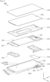
- the electronic device 100 may include a first plate (or first housing portion) 120, second plate (or second housing portion) 130, first support member 211 (e.g., bracket), display 101, first substrate assembly 241, second substrate assembly 242, battery 250, second support member 261, third support member 262, or antenna structure 270.
- the electronic device 100 may omit at least one (e.g., the first support member 211, the second support member 261, or the third support member 262) of the components or may additionally include other components.
- At least one of the components of the electronic device 100 may be the same as or similar to at least one of the components of the electronic device 100 of FIGS. 1A or 1B , and repeated descriptions thereof will be omitted below.
- the display 101 may be, for example, coupled to one surface of the first support member 211 and be disposed between the first support member 211 and the first plate 120.
- the first substrate assembly 241 and the second substrate assembly 242 may be, for example, coupled to the other surface of the first support member 211 and be interposed between the first support member 211 and the second plate 130.
- the second substrate assembly 242 when viewed from above the first plate 120, the second substrate assembly 242 may be disposed to be spaced apart from the first substrate assembly 241 with the battery 250 interposed therebetween.
- the second substrate assembly 242 may include a second printed circuit board electrically connected to the first printed circuit board of the first substrate assembly 241.
- the second substrate assembly 242 may include various electronic components electrically connected to the second printed circuit board.
- An electronic component may be disposed at the second printed circuit board or may be electrically connected to the second printed circuit board through an electrical path such as a cable or an FPCB.
- the electronic component may include a USB connector using the first connector hole 108, an earphone jack using the second connector hole 109, a microphone using the microphone hole 203, or a speaker using a speaker hole 207.
- the third support member 262 when viewed from above the first plate 120, the third support member 262 may be disposed to be spaced apart from the second support member 261 with the battery 250 interposed therebetween.
- the third support member 262 may be disposed between the first support member 211 and the second plate 130, and be coupled to the first support member 211 through a fastening element such as a bolt.
- At least a portion of the second substrate assembly 242 may be disposed between the first support member 211 and the third support member 262, and the third support member 262 may cover the second substrate assembly 242 for protection.
- the conductive pattern of the antenna structure 270 may be electrically connected to a wireless communication circuit disposed at the first substrate assembly 241.
- the conductive pattern may be used for short-range wireless communication such as near field communication (NFC).
- the conductive pattern may be used for magnetic secure transmission (MST) for transmitting and/or receiving a magnetic signal.
- NFC near field communication
- MST magnetic secure transmission
- the display 101 may include an opening 1011 formed in at least a partial area corresponding to an optical sensor (e.g., the first camera device 105 or the biometric sensor) disposed inside the electronic device 100.
- the opening 1011 may be formed as, for example, a notch shape.
- the opening 1011 may be implemented in the form of a through hole.
- the optical sensor may receive external light through the opening 1011 of the display 101 and a partial area of the first plate 120 aligned therewith.
- the opening 1011 of the display 101 may be replaced with a substantially transparent area formed by changing a pixel structure and/or a wiring structure.
- the second plate 130 may include a first surface 131 (see FIG. 1B ) including the rear surface 110B and the side surface 110C and a second surface 132 disposed opposite to the first surface 131.
- the second surface 132 may be formed in a shape along the first surface 131 and include, for example, a portion 110D along the rear surface 110B and a portion 110E along the side surface 110C.
- the housing 110 may include a rear plate forming the rear surface 110B and a side bezel structure (or side member) forming the side surface 110C instead of the second plate 130.
- the rear plate and the side bezel structure may include a fine pattern that enables viewing of monochromatic lights of visible light through a spectrum.
- FIGS. 4A and 4B are cross-sectional views illustrating a die 400 according to an embodiment.
- the die 400 may include a first template 410, a second template 420, or a core block (or core) 430.
- the first template 410 may be a mold base including a cavity in which a molten resin may flow.
- the first template 410 may be a fixed bolster plate or a cavity plate.
- the first template 410 may include the cavity, which is an empty space in the form of a hollow in a direction from the second template 420 toward the first template 410 (e.g., +z axis direction).
- a cavity block including a cavity may be disposed at the first template 410 instead of a structure of forming a cavity in the first template 410.
- the core block 430 may include a third molding surface 431 that serves to form a second surface of a mold-injected structure.
- the molding space 500 may be formed by the first molding surface 411, the second molding surface 421, and the third molding surface 431.
- the die is not limited to the embodiment of FIGS. 4A and 4B , and may be implemented in various other structures to form the molding space 500.
- the gate 450 and/or the runner 460 may be formed, for example, in a space between the first template 410 and the second template 420 in a closed state of the die 400, as illustrated in FIGS. 4A and 4B .
- the position, number, or shape of gates or runners is not limited to the embodiment of FIG. 4A and may be various.
- the first curved space 521, the second curved space 522, the third curved space 523, and the fourth curved space 524 may be curved in a -z axis direction.
- the first curved space 521 and the second curved space 522 may be extended parallel to each other.
- the third curved space 523 and the fourth curved space 524 may be extended parallel to each other.
- the first curved space 521 may connect one end of the third curved space 523 and one end of the fourth curved space 524
- the second curved space 522 may connect the other end of the third curved space 523 and the other end of the fourth curved space 524.
- the molding space 500 may include a curved corner space connecting the first curved space 521 and the third curved space 523, a curved corner space connecting the first curved space 521 and the fourth curved space 524, a curved corner space connecting the second curved space 522 and the third curved space 523, and a curved corner space connecting the second curved space 522 and the fourth curved space 524.
- the first curved space 521 and the second curved space 522 when viewed in an x-z cross-section, may be at least partially symmetrical to each other with the flat space 510 interposed therebetween.
- the third curved space 523 and the fourth curved space 524 may be at least partially symmetrical to each other with the flat space 510 interposed therebetween.
- the die parting line 401 may be positioned so that one surface of the curved spaces 521, 522, 523, and 524 may be formed by the first molding surface 411 of the first template 410 and the second molding surface 421 of the second template 420.
- the die parting line 401 and the gate 450 related thereto according to the embodiment of FIG. 5 prevent the die 400 from having a locking structure such as an undercut; thus, the mold-injected structure may be taken out from the die 400.
- a molten resin may be injected into the molding space 500 in a state in which the die 400 is closed, as illustrated in FIGS. 4A and 4B .
- the molten resin occupying the molding space may be solidified by circulating cooling water through the die 400.
- the mold-injected structure may be disposed at the core block 430.
- the mold-injected structure may include an extension portion formed through the gate 450. When an ejector pin pushes the extension portion, the mold-injected structure may be separated from the core block 430.
- the gate 450 may be formed as a fan gate.
- the fan gate when viewed in the -z axis direction, is a gate in a form in which a portion connected to the molding space 500 is widened, and a flow tip thereof may be formed to be wide and uniform.
- the fan gate may reduce molding defects when the structure is mold-injected through the molding space 500 of a form having the flat space 510 and the curved spaces 521, 522, 523, and 524.
- the second template 420 may include one side space 425 of the gate 450.
- the one side space 425 may have a shape in which a width in the y-axis direction increases toward a portion connected to the molding space 500.
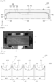
- a pattern 600 (e.g., uneven surface) including a plurality of dimples 611, 612, 613, and 614 may be formed at the third molding surface 431 of the core block 430.
- the dimples may refer to recessed grooves. According to certain embodiments, dimples may be referred to by other terms of the same level, such as a pit or a recess. According to an embodiment, the dimple may separate a spectrum of light according to a wavelength by a diffraction phenomenon of light. According to certain embodiments, the plurality of dimples may be arranged in various directions along at least a portion of the third molding surface 431.
- some of the plurality of dimples 611, 612, 613, and 614 and other dimples may be formed in different shapes.
- some of the diameters A1, A2, A3, and A4 of the plurality of dimples 611, 612, 613, and 614 may be different from others.
- some of the depths H1, H2, H3, and H4 of the plurality of dimples 611, 612, 613, and 614 may be different from others.
- a cross-sectional shape of some of the plurality of dimples and a cross-sectional shape of others thereof may be different from each other.
- FIGS. 7A, 7B, and 7C are cross-sectional views illustrating patterns formed at a third molding surface 431 of a core block 430 according to certain embodiments.
- FIG. 8 is a diagram illustrating a third molding surface 431 including a pattern 800 according to certain embodiments.
- the pattern 800 may include a plurality of slits 811, 812, 813, 814, and 815 arranged at intervals.
- the slit 811, 812, 813, 814, or 815 may have various cross-sectional shapes such as a rectangle, a trapezoid, or a triangle.
- the third molding surface 431 of the core block 430 may have surface roughness having a height of about 1 ⁇ m or less by the pattern 600.
- the depths H1, H2, H3, and H4 of the plurality of dimples 611, 612, 613, and 614 may be formed in about 1 ⁇ m or less.
- depths H11, H12, H13, and H14 of the plurality of dimples 711, 712, 713, and 714 are formed in about 1 ⁇ m or less, and the third molding surface 431 of the core block 430 may have surface roughness having a height of about 1 ⁇ m or less.
- the depths of the plurality of slits 811, 812, 813, 814, and 815 are formed in about 1 ⁇ m or less; thus, the third molding surface 431 of the core block 430 may have surface roughness having a height of about 1 ⁇ m or less.
- burrs may be, for example, a residue remaining in a protruding shape around dimples or slits after forming the dimples or slits. Because the pulse width equal to or less than the preset or specified value is shorter than a heat propagation time of a material forming the core block 430, thermal damage or structural change of the material may not be caused, thereby reducing occurrence of the burr.
- a laser may be radiated to the core block 430 within an extremely short time, such as a pulse width equal to or less than the preset or specified value; thus, a heat diffusion phenomenon may be reduced to reduce occurrence of the burr.
- a laser having a pulse width less than or equal to the preset or specified value may include a femto second laser.
- the femto second laser may refer to a laser having a pulse width having "ultrashort" pulses, less than a picosecond, and defined in the domain of femtoseconds (10 -15 seconds).
- the plurality of slits 811, 812, 813, 814, and 815 of FIG. 8 are formed using a femtosecond laser, generation of burrs may be reduced.
- a pattern is formed using a laser having a pulse width equal to or less than the preset or specified value, residues may be generated around the dimples or slits, but such residues may be in the form of fine powder that may be easily removed by washing.
- a dimple 900 is formed using a laser (e.g., femtosecond laser) having a pulse width equal to or less than a preset or specified value, residuals such as burrs may be prevented from formation in a peripheral portion 901 of the dimple 900.
- a laser e.g., femtosecond laser
- burrs are prevented from forming at the third molding surface 431 of the core block 430 illustrated in FIG. 5 , and a pattern having surface roughness having a height of about 1 ⁇ m or less may be formed.
- One surface of the structure mold-injected through the die 400 of FIG. 4A may have a pattern in which the third molding surface 431 of the core block 430 is imprinted.
- One surface in which the pattern is disposed in the mold-injected structure may have surface roughness having a height of about 1 ⁇ m or less to correspond to the pattern of the third molding surface 431.
- the surface roughness may be the maximum value average roughness in which a maximum height Rmax from a lowest point to a highest point is about 1 ⁇ m or less.
- one surface in which the pattern is disposed may have surface roughness of about 0.1 ⁇ m to 1 ⁇ m.
- one surface in which the pattern is disposed separates a spectrum of light according to a wavelength by a diffraction phenomenon of light to enable viewing of monochromatic lights of visible light.
- a dimple may be formed at the molding surface of the die using a microsecond laser.
- a laser e.g., femtosecond laser
- a dimple is formed using a microsecond laser having a pulse width of microseconds (10 -6 seconds)
- residues such as burrs may be formed in a periphery of the dimple.
- burrs may be formed at the periphery of the dimple.
- dimples may be formed at the molding surface of the die using chemical corrosion.
- a laser e.g., femtosecond laser
- residues such as burrs may be formed at the periphery of the dimple.
- dimples may be formed at the molding surface of the die using electrical corrosion.
- a laser e.g., femtosecond laser
- residues such as burrs may be formed at the periphery of the dimple.
- the pattern imprinted in the mold-injected structure through the die 400 of FIG. 4A may have a shape rendering formation of a spectrum difficult because of the presence of burrs.
- a structure for the housing of the electronic device may be injection molded through the die (e.g., the die 400 of FIG. 4A ).
- FIG. 10 is a plan view illustrating a structure 1000 that is mold-injected through the die illustrated in FIG. 4A , according to an embodiment.
- the mold-injected structure 1000 may include a flat portion 1010 and a curved border portion 1020 extending at least partially along an edge of the flat portion 1010.
- the flat portion 1010 may be formed through the flat space 510 of the molding space 500.
- a first distance D1 in which the first curved border 1021 and the second curved border 1022 are spaced apart from each other may be different from a second distance D2 in which the third curved border 1023 and the fourth curved border 1024 are spaced apart from each other.
- the first distance D1 may be smaller than the second distance D2.
- the mold-injected structure 1000 may include a mark (e.g., parting line (not illustrated)) formed along the die parting line 401 because of the die parting line 401 of the die 400 illustrated in FIG. 4A .
- the mold-injected structure 1000 may include an extension portion 1030 corresponding to the gate 450 (e.g., fan gate) of FIG. 4A disposed along at least a portion of the die parting line.
- the extension portion 1030 may be connected to the second curved border 1022.
- the extension portion 1030 may be removed through post-processing.
- the die may include, for example, a space (e.g., auxiliary cavity) connected to the molding space, so as to receive an overflow of the molten resin when the resin is filled into the molding space (e.g., the molding space 500 of FIG. 4A or 4B ) through a gate.
- the structure 1100 mold-injected through the die may include an extension portion 1130 of a shape at least partially disposed along the curved border portion 1020, when viewed from above the flat portion 1010 (e.g., viewed in the z-axis direction).
- the extension portion 1130 may be made of the molten resin that overflows during injection molding through the die.
- post-processing of a structure mold-injected through the die may be performed.
- FIG. 12 is a diagram illustrating at least a portion of a state in which an extension portion 1030 formed by a gate of a die is removed from the structure 1000 of FIG. 10 according to an embodiment.
- a trace 1200 of an area where the extension portion 1030 is removed may remain at a surface 1201 of the second curved border 1022.
- the structure 1000 may include a first surface 1001 (e.g., the first surface 131 of FIG. 1B ) and a second surface 1002 (e.g., the second surface 132 of FIG. 2 ) disposed opposite to the first surface 1001.
- film lamination, coating, or polishing may be performed at the first surface 1001 of the structure 1000.
- the second surface 1002 may have a pattern formed by imprinting a molding surface (e.g., the third molding surface 431 of FIG. 5 ) of the die.
- a material used for film lamination or coating in relation to the trace 1200 may be selected in consideration of transparency.
- various post-processes e.g., film lamination, coating, or polishing
- various post-processes may be performed to reduce the degree to which the removal trace is visible.
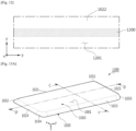
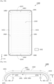
- FIG. 13A is a diagram illustrating a plate 1300 formed by removing the extension portion 1030 formed by the gate of the die from the structure 1000 of FIG. 10 according to an embodiment.
- FIG. 13B is a plan view illustrating a plate 1300 of FIG. 13A according to an embodiment.
- the second housing portion 130 may be formed based on the plate 1300 of FIG. 13A , and the curved border portion 1020 may be seamlessly extended with bending from the flat portion 1010 toward the first plate 120.
- the plate 1300 may be formed to be substantially transparent and include, for example, various materials such as glass or polymer.
- the second surface 1002 may include a first edge 1051, a second edge 1052 extended opposite to the first edge 1051, a third edge 1053 connecting one of the first edge 1051 and one of the second edge 1052, and a fourth edge 1054 connecting the other end of the first edge 1051 and the other end of the second edge 1052 and extended opposite to the third edge 1053.
- the second surface 1002 may include a first plane 1050 formed by the flat portion 1010, a first curved surface 1061 adjacent first edge 1051 and formed by the first curved border 1021, a second curved surface 1062 adjacent second edge 1052 and formed by the second curved border 1022, a third curved surface 1063 adjacent edge 1053 and formed by the third curved border 1023, or a fourth curved surface 1064 adjacent fourth edge 1054 and formed by the fourth curved border 1024.
- the first plane 1050 may include a first boundary 1055 connected to a first curved surface 1061, a second boundary 1056 connected to the second curved surface 1062, a third boundary 1057 connected to a third curved surface 1063, or a fourth boundary 1058 connected to a fourth curved surface 1064.
- the first boundary 1055 and the second boundary 1056 may be parallel, and the third boundary 1057 and the fourth boundary 1058 may be parallel.
- the first curved surface 1061 may extended, for example, from the first boundary 1055 to the first edge 1051 to seamlessly connect to the first plane 1050.
- the first edge 1051 may be disposed apart from the first boundary 1055 by a first height H1 in a +z axis direction, which is the direction of the first plane 1050.
- the first edge 1051 may be disposed apart from the first boundary 1055 by a first width W1 in the +x axis direction perpendicular to the +z axis direction.
- the shape of the first curved surface 1061 may vary according to a curvature of each point between the first boundary 1055 and the first edge 1051.
- the second curved surface 1062 may be extended, for example, from the second boundary 1056 to the second edge 1052 to be seamlessly connected to the first plane 1050.
- the second edge 1052 may be disposed apart from the second boundary 1056 by a second height H2 in the +z axis direction.
- the second edge 1052 may be disposed apart from the second boundary 1056 by a second width W2 in the -x axis direction.
- the shape of the second curved surface 1062 may vary according to a curvature of each point between the second boundary 1056 and the second edge 1052.
- the first curved surface 1061 and the second curved surface 1062 may be symmetrical with one another, and with the first plane 1050 interposed therebetween.
- the fourth curved surface 1064 may be, for example, extended from the fourth boundary 1058 to the fourth edge 1054 to seamlessly connect to the first plane 1050.
- the fourth edge 1054 may be disposed apart from the fourth boundary 1058 by a fourth height H4 in the +z axis direction.
- the fourth edge 1054 may be disposed apart from the fourth boundary 1058 by a fourth width W4 in the -y axis direction.
- the shape of the fourth curved surface 1064 may vary according to a curvature of each point between the fourth boundary 1058 and the fourth edge 1054.
- the third curved surface 1063 and the fourth curved surface 1064 may be symmetrical to one another, with the first plane 1050 interposed therebetween.
- At least two of the first height H1, the second height H2, the third height H3, and the fourth height H4 may be different from each other.
- the second surface 1002 may include a first corner curved surface 1081 that seamlessly connects a first curved surface 1061 and a third curved surface 1063 at the first corner 1031.
- the second surface 1002 may include a second corner curved surface 1082 that seamlessly connects the first curved surface 1061 and a fourth curved surface 1064 at the second corner 1032.
- the second surface 1002 may include a third curved surface 1083 that seamlessly connects a second curved surface 1062 and the third corner curved surface 1063 at the third corner 1033.
- the second surface 1002 may include a fourth corner curved surface 1084 that seamlessly connects the second curved surface 1062 and the fourth curved surface 1064 at the fourth corner 1034.
- a shape of the first surface 1001 may vary according to a thickness of the plate 1300 from the first edge 1051 to the second edge 1052.
- a shape of the first surface 1001 may vary according to a thickness of the plate 1300 from the third edge 1053 to the fourth edge 1054.
- FIG. 15 is a cross-sectional view illustrating a pattern formed at the second surface 1002 of the plate 1300 of FIG. 13A according to an embodiment.
- the second surface 1002 of the plate 1300 may have a pattern 1500 in which the third molding surface 431 of the core block 430 is imprinted.
- the pattern 1500 may include protrusions 1511, 1512, 1513, and 1514 having a convex shape, in a direction oriented from the first surface 1001 (see FIG. 14A or 14B ) to the second surface 1002, so as to correspond to the plurality of dimples 611, 612, 613, and 614 of FIG. 6 .
- FIG. 15 illustrates only a part of the second surface 1002, and the pattern 1500 may be formed in at least a part of the second surface 1002.
- the pattern 1500 may be formed in at least a portion of the first plane 1050, the first curved surface 1061, the second curved surface 1062, the third curved surface 1063, the first corner curved surface 1081, the second corner curved surface 1082, the third corner curved surface 1083, and/or the fourth corner curved surface 1084 of FIG. 13B .
- the plate 1300 mold-injected through the die may be implemented with a material capable of passing light.
- the pattern 1500 separates a spectrum of light according to a wavelength by a diffraction phenomenon of light to implement a visual surface texture that makes monochromatic lights of visible light visible.
- the mold-injected plate 1300 may be implemented with various materials.
- the mold-injected plate 1300 has light transmittance of 70% or more and/or may have a haze value of about 20% or less so that the visual surface texture by a spectrum may be visible.
- post-processing according to operation 330 may include processing of disposing various layers at the second surface 1002 of the plate 1300 illustrated in FIG. 13B .
- FIG. 16 is a cross-sectional view illustrating the second housing portion 130 of FIG. 2 according to an embodiment.
- the first color layer 1610 is a translucent thin film layer and may implement a color. According to certain embodiments, the first color layer 1610 may serve to increase surface reflectivity.
- the first color layer 1610 may be disposed at the second surface 1002 of the plate 1300 through various deposition methods such as physical vapor deposition (PVD). Physical vapor deposition may vaporize various metal materials such as indium, titanium oxide, aluminum oxide, or silicon oxide in a vacuum, thereby coating vaporized metal atoms on the second surface 1002 of the plate 1300.
- PVD physical vapor deposition
- the second color layer 1620 is an opaque thin film layer and may implement a color. A color of the second color layer 1620 may make a color of the first color layer 1610 appear darker.
- the second housing portion 130 is disposed at the electronic device (e.g., the electronic device 100 of FIG. 1A )
- the second color layer 1620 may serve as a shield to hide the inside of the electronic device.
- At least one layer included in the decoration layer 1600 may include various materials for shielding electromagnetic waves (e.g., EMI shielding).
- the second housing portion 130 may further include various other layers, or some layers may be omitted. According to certain embodiments (not illustrated), the second housing portion 130 may be disposed at the first surface 1001 (see FIGS. 14A and 14B ) of the plate 1300 to include various layers for visual effects (see FIG. 12 ). According to certain embodiments (not illustrated), the stacking order of the first color layer 1610 and the second color layer 1620 may be changed.
- the second housing portion 130 may have a plurality of first color layers or a plurality of second color layers.
- the pattern 1500 e.g., diffraction grating
- the pattern 1500 formed at the second surface 1002 separates a spectrum of light according to a wavelength by a diffraction phenomenon of light to implement a visual surface texture that makes monochromatic lights 1602 of visible light visible. Because of a thickness between the first surface 1001 and the second surface 1002 and the pattern 1500 formed at the second surface 1002, a visual surface texture having a sense of depth may be visible.
- a material of the plate 1300 and/or the decoration layer 1600 may be selected in consideration of a refractive index between the plate 1300 and the decoration layer 1600. As the refractive index difference between the plate 1300 and the decoration layer 1600 increases, reflectivity of the interface between the plate 1300 and the decoration layer 1600 may increase. For example, as reflectivity of the interface between the plate 1300 and the decoration layer 1600 increases, an amount of light reflected and/or diffracted at the interface increases, thereby making it easier to implement a visual surface texture. According to certain embodiments, at least a portion of the decoration layer 1600 may include various reflective materials.
- the pattern 1500 of the second surface 1002 of the plate 1300 in which the pattern formed at the third molding surface 431 is imprinted may include pattern shapes 1671, 1672, and 1673 by the burrs. These pattern shapes 1671, 1672, and 1673 may make formation of a spectrum difficult. Further, the pattern shapes due to the burrs may enable the second surface 1002 to have surface roughness in which heights H51, H52, and H53 exceed about 1 ⁇ m.
- FIG. 17 is a diagram illustrating a cross-sectional curve 1700 of the plate 1300 of FIG. 13A according to an embodiment.
- a pattern e.g., the pattern 1500 of FIG. 15
- the second surface 1002 see FIG. 13A
- the plate 1300 may have surface roughness having a height of about 1 ⁇ m or less (e.g., about 0.333 ⁇ m).
- FIGS. 18A , 18B, and 18C are diagrams illustrating various visual surface textures viewed through the second housing portion 130 of FIG. 2 according to certain embodiments.
- the pattern formed at the second surface 1002 of the plate 1300 illustrated in FIG. 13B may vary according to a pattern formed at the molding surface of the die. Based on various patterns formed at the second surface 1002 of the plate 1300 illustrated in FIG. 13B , various visual surface textures through a spectrum may be viewed as illustrated in FIG. 18A , 18B, or 18C .
- residues such as burrs may be formed at the periphery of the dimple.
- a surface of the structure on which the molded surface is imprinted through injection molding may have difficulty in separating a spectrum of light according to a wavelength because of the burrs.
- a pattern (e.g., the pattern 600 of FIG. 6 , the pattern 701 of FIG. 7A , the pattern 702 of FIG. 7B , the pattern 703 of FIG. 7C , or the pattern 800 of FIG. 8 ) may be formed in at least a portion of the first molding surface 411 and the second molding surface 421 of the die 400.
- the first surface 1001 of the plate e.g., the plate 1300 of FIG. 16
- mold-injected through the die 400 may have a pattern in which the first molding surface 411 and/or the second molding surface 421 is imprinted.
- Various layers such as the decoration layer 1600 of FIG. 16 may be disposed at the first surface 1001.
- a visual surface texture in which monochromatic lights of visible light are visible may be implemented through the first surface 1001 including the pattern.
- a pattern for facilitating a spectrum by reducing occurrence of burrs may be formed.
- a surface of a structure having a pattern formed using a laser having a pulse width less than or equal to the preset or specified value may have surface roughness forming a height of about 1 ⁇ m or less.
- the housing forming an external shape of the electronic device may be produced by a method of forming a UV molding layer having a fine pattern at the surface of the structure through UV molding.
- a UV molding liquid e.g., UV curable resin
- the housing may be produced by disposing a film having a fine pattern in the die and then injecting a resin to form a member bonded to the film.
- a resin to form a member bonded to the film.
- the housing (e.g., the second housing portion 130 of FIG. 2 ) may not use a film having a fine pattern or a layer through UV molding and may have a fine pattern for a visual surface texture without restrictions on the surface shape of the housing.
- FIG. 19 is a cross-sectional view illustrating the second housing portion 130 of FIG. 2 according to another embodiment.
- the visual effect may include, for example, various visual characteristics such as a visual texture (or visual surface texture), a visual pattern, or a visual color that the user feels for the second housing portion 130 when viewed toward the first surface 1001.
- various visual effects may be provided to the user because of medium characteristics of a structure (e.g., layer structure) formed with a plurality of layers included in the second housing portion 130.
- the visual effect may be, for example, implemented in various ways based on various light phenomena in which light incident on the first surface 1001 is reflected, refracted, scattered, or dispersed by the layer structure of the second housing portion 130.
- the visual effect may be variously implemented based on, for example, light transmittance and refractive index of each layer, and reflectivity at an interface between layers.
- the laminated film may be bonded to the plate 1300.
- the second layer 1920 may be disposed at the laminated film.
- a primer may be positioned between the plate 1300 and the transparent adhesive layer 1912. After applying a primer to the second surface 1002 of the plate 1300, the first layer 1910 may be bonded to the primer.
- the plate 1300 and the transparent adhesive layer 1912 may be bonded to each other without gaps or bubbles by the primer.
- the primer may be, for example, formed in a thin film of about 1 ⁇ m or less having a shape following the first pattern (e.g., the pattern 1500 of FIG. 15 ) of the second surface 1002 of the plate 1300.
- the primer may include a material having bonding affinity with the plate 1300 and the transparent adhesive layer 1912.
- the primer may have a color, and when light is incident on the first surface 1001, a visually unique color of the second housing portion 130 may be implemented by the primer.
- the base film 1911 is, for example, a film that serves as a basis for disposing at least one layer, and may be, for example, formed with various polymers such as polycarbonate (PC) or polyethylene terephthalate (PET).
- the base film (or polymer film) 1911 may include a substantially transparent or translucent material.
- a transparent adhesive layer 1912 for bonding to the plate 1300 may be disposed at one surface of the base film 1911, and the pattern layer 1913 may be disposed at the other surface of the base film 1911.
- the visual effect by the first layer 1910 may be substantially implemented by the pattern layer 1913.
- the pattern layer 1913 may be formed through UV molding.
- the pattern layer 1913 e.g., UV molding layer
- the UV molding layer may have a second pattern in which a die pattern (e.g., uneven pattern) is substantially imprinted.
- the second pattern may include, for example, an uneven surface including a plurality of dimples or a plurality of slits.
- the second pattern of the UV molding layer may be, for example, positioned at an interface between the first layer 1910 and the second layer 1920.
- a primer may be positioned between the base film 1911 and the UV molding layer (e.g., the pattern layer 1913).
- a molding layer e.g., UV molding layer
- a second pattern may be formed by applying a primer to the base film 1911, applying a photocurable resin to the primer, and radiating light (e.g., ultraviolet rays) in a designated band to a photocurable resin.
- the base film 1911 and the UV molding layer may be bonded without gaps or bubbles by the primer.
- the primer may include a material having bonding affinity with the base film 1911 and the UV molding layer.
- the second pattern of the UV molding layer may implement a visual texture that enables viewing of monochromatic lights of visible light by separating a spectrum of light according to a wavelength by a diffraction phenomenon of light.
- the second pattern e.g., diffraction grating
- the second pattern formed at the interface may implement a visual texture that enables viewing of monochromatic lights of visible light by separating a spectrum of light according to a wavelength by a diffraction phenomenon of light.
- the pattern layer 1913 may include a gradient pattern for a visual effect of the gradient.
- the gradient pattern may be printed on the base film 1911.
- the pattern layer 1913 may include a UV molding layer and a layer including a gradient pattern.
- the layer including the gradient pattern may be, for example, positioned between the base film 1911 and the UV molding layer.
- the second pattern of the UV molding layer may be positioned at an interface between the first layer 1910 and the second layer 1920.
- the transparent adhesive layer 1912 may include, for example, an optically transparent adhesive material such as an optical clear adhesive (OCA).
- OCA optical clear adhesive
- a release film protecting the transparent adhesive layer 1912 may be separated, thereby exposing the transparent adhesive layer 1912.
- the transparent adhesive layer 1912 may reduce an air gap between the plate 1300 and the base film 1911.
- deformation or loss of light may occur because of the difference in refractive index between different media (e.g., the plate 1300, air gap, and the base film 1911); thus, a quality of the visual effect by the plate 1300, the first layer 1910, and/or the second layer 1920 may be deteriorated.
- the difference in refractive index between the transparent adhesive layer 1912 and a medium layer in contact therewith may be reduced; thus, reflectivity of the interface between the transparent adhesive layer 1912 and the medium layer in contact therewith may be deteriorated. Accordingly, it is possible to reduce reflection at the interface and deformation or loss of light resulting therefrom, thereby securing a quality of the visual effect by the plate 1300, the first layer 1910, and/or the second layer 1920.
- the first color layer 1921 may implement, for example, a color as a translucent thin film layer.
- the first color layer 1921 may serve to increase surface reflectivity.
- the first color layer 1921 may be disposed at the first layer 1910 through various deposition methods such as physical vapor deposition (PVD).
- PVD physical vapor deposition
- various metal materials such as indium, titanium oxide, aluminum oxide, or silicon oxide may be vaporized in a vacuum so that vaporized metal atoms may be coated on the surface of the first layer 1910.
- the second color layer 1922 may implement, for example, a color as an opaque thin film layer.
- the color of the second color layer 1922 may make the color of the first color layer 1921 appear darker.
- the second housing portion 130 is disposed at the electronic device (e.g., the electronic device 100 of FIG. 1A )
- the second color layer 1922 may serve as a shield to prevent the inside of the electronic device from being viewed.
Landscapes
- Engineering & Computer Science (AREA)
- Signal Processing (AREA)
- Manufacturing & Machinery (AREA)
- Mechanical Engineering (AREA)
- Microelectronics & Electronic Packaging (AREA)
- Telephone Set Structure (AREA)
Description
- An embodiment of the disclosure relates to electronic devices, and more particular, to an electronic device having a housing on which patterns are deposited during manufacturing.
- Design aesthetics increasingly differentiate competing electronic devices to consumers, as these devices become increasingly upscale in specification. As a result, there is impetus to form the external housing of these devices to produce a visually pleasing design with a luxurious texture.
- For example, a visually pleasing surface texture may be implemented by disposing a film (e.g., a deco film) on a surface of the housing.
- The surface of the housing may be formed having a shape including edges or corners where several different surfaces meet. When a flat-shaped film is bonded to the surface, the film does not adhere evenly at the edges or corners, resulting in a bonding failure such as folding or wrinkles.
- In another example, the visual surface texture may be implemented by disposing a patterned layer on a surface of the housing through ultraviolet (UV) molding. However, when the surface of the housing is not flat, and includes edges or corners where several disparate surfaces meet, it may be difficult to perform a uniform rolling application of the molding liquid (e.g., a UV curable resin) to form the layer properly on the surface during UV molding.
- An embodiment of the disclosure provides an electronic device including a housing and a method of producing the housing for easily implementing a visual surface texture without a restriction on a surface shape of the housing.
- According to an embodiment of the disclosure, an electronic device includes a housing including: a first plate forming a front surface of the housing, a second plate integrally forming a rear surface and side surface of the housing, wherein a space is enclosed between the front surface, side surface and rear surface, and wherein the second plate includes a first surface forming the side and rear surfaces of the housing, and a second surface disposed opposite to the first surface, and a display disposed in the space and at least partially visible through the first plate, wherein at least a portion of the second surface includes a pattern having surface roughness having a height of 0.1 µm to 1 µm, and wherein the second plate includes a light transmittance rate of 70% to 100%.
- According to certain embodiments of the disclosure, an electronic device includes a housing defining a front surface, a rear surface, and a side surface, and a space enclosed between the front surface and the rear surface, wherein the housing includes: a first plate forming the front surface, a second plate forming the rear surface and the side surface, integrally extending from the side surface to the rear surface, wherein the second plate includes a first surface forming the rear surface and a second surface disposed opposite to the first surface, a first layer bonded to the second plate within the space and including at least one pattern, wherein the first layer is disposed at the second surface between the second surface and the second layer, and a second layer bonded to the first layer, the second layer including at least one color; and a display disposed in the space and at least partially visible through the first plate, wherein at least a portion of the second surface includes a pattern having surface roughness having a height of 0.1 µm to 1 µm.
- According to an embodiment of the disclosure, by forming a pattern having surface roughness having a height of about 0.1 µm to 1 µm at the surface of the housing, a visual surface texture can be implemented using a diffraction phenomenon without a restriction on a surface shape and without a film or a UV molding layer having a fine pattern.
- In addition, effects obtained or predicted by certain embodiments of the disclosure will be disclosed either directly or implicitly in the detailed description of the embodiments of the disclosure. For example, various effects predicted according to certain embodiments of the disclosure will be disclosed within the detailed description to be described later.
- In the drawings, the same or similar reference numerals may be used for the same or similar components.
-
FIG. 1A is a perspective view illustrating a front surface of a mobile electronic device according to an embodiment. -
FIG. 1B is a perspective view illustrating a rear surface of the electronic device ofFIG. 1A according to an embodiment. -
FIG. 2 is an exploded perspective view illustrating the electronic device ofFIG. 1A according to an embodiment. -
FIG. 3 is a flowchart illustrating a production flow of a cover according to an embodiment. -
FIGS. 4A and4B are cross-sectional views illustrating a die according to an embodiment. -
FIG. 5 is a diagram illustrating a second template and a core block of a die according to an embodiment. -
FIG. 6 is a cross-sectional view illustrating a pattern formed at a third molding surface of a core block according to an embodiment. -
FIGS. 7A, 7B, and 7C are cross-sectional views illustrating patterns formed at a third molding surface of a core block according to certain embodiments. -
FIG. 8 is a diagram illustrating a third molding surface including a pattern according to certain embodiments. -
FIG. 9 is a diagram illustrating a dimple formed at a third molding surface ofFIG. 5 using a laser having a pulse width equal to or less than a preset or specified value according to an embodiment. -
FIG. 10 is a plan view illustrating a structure mold-injected through the die ofFIG. 4A according to an embodiment. -
FIG. 11 is a plan view illustrating a structure mold-injected through a die according to certain embodiments. -
FIG. 12 is a diagram illustrating a state in which an extension portion formed by a gate of a die is removed from the structure ofFIG. 10 according to an embodiment. -
FIG. 13A is a diagram illustrating a plate formed by removing an extension portion formed by a gate of a die from the structure ofFIG. 10 according to an embodiment. -
FIG. 13B is a plan view illustrating the plate ofFIG. 13A according to an embodiment. -
FIG. 14A is a cross-sectional view taken along line C-C' in the plate ofFIG. 13A according to an embodiment. -
FIG. 14B is a cross-sectional view taken along line D-D' in the plate ofFIG. 13A according to an embodiment. -
FIG. 15 is a cross-sectional view illustrating a pattern formed at a second surface of the plate ofFIG. 13A according to an embodiment. -
FIG. 16 is a cross-sectional view illustrating a second housing portion ofFIG. 2 according to an embodiment. -
FIG. 17 is a graph illustrating a cross-sectional curve of the plate ofFIG. 13A according to an embodiment. -
FIGS. 18A ,18B, and 18C are diagrams illustrating various visual surface textures viewed through the second housing portion ofFIG. 2 according to certain embodiments. -
FIG. 19 is a cross-sectional view illustrating a second housing portion ofFIG. 2 according to another embodiment. - The following description with reference to the accompanying drawings is provided to assist in a comprehensive understanding of certain embodiments of the disclosure as defined by the claims and their equivalents. It includes various specific details to assist in that understanding but these are to be regarded as mere examples. Accordingly, those of ordinary skill in the art will recognize that various changes and modifications of the certain embodiments described herein can be made without departing from the disclosure. In addition, descriptions of well-known functions and implementations are omitted for clarity and conciseness.
- The terms and words used in the following description and claims are not limited to the bibliographical meanings, but, are merely used by the inventor to enable a clear and consistent understanding of the disclosure. Accordingly, it should be apparent to those skilled in the art that the following description of certain embodiments of the disclosure is provided for illustration purpose only and not for the purpose of limiting the disclosure as defined by the appended claims and their equivalents.
- With regard to the description of the drawings, similar reference numerals may be used to refer to similar or related elements.
- A singular form of a noun corresponding to an item may include one or more of the things, unless the relevant context clearly indicates otherwise. As used herein, each of such phrases as "A or B", "at least one of A and B", "at least one of A or B", "A, B, or C", "at least one of A, B, and C", and "at least one of A, B, or C" may include any one of, or all possible combinations of the items enumerated together in a corresponding one of the phrases.
- As used herein, such terms as "1st" and "2nd", or "first" and "second" may be used to simply distinguish a corresponding component from another, and does not limit the components in other aspect (e.g., importance or order). If an element (e.g., a first element) is referred to, with or without the term "operatively" or "communicatively", as "coupled with", "coupled to", "connected with", or "connected to" another element (e.g., a second element), it means that the element may be coupled with the other element directly (e.g., wiredly), wirelessly, or via a third element.
- An electronic device according to an embodiment may be one of various types of electronic devices. The electronic device may include a portable communication device (e.g., a smart phone), a computer device, a portable multimedia device, a portable medical device, a camera, a wearable device, or a home appliance. However, the electronic device is not limited to any of those described above.
-
FIG. 1A is a perspective view illustrating a front surface of a mobileelectronic device 100 according to an embodiment of the disclosure. -
FIG. 1B is a perspective view illustrating a rear surface of theelectronic device 100 ofFIG. 1A according to an embodiment of the disclosure. - Referring to
FIGS. 1A and 1B , according to an embodiment, anelectronic device 100 may include ahousing 110 that includes afront surface 110A, arear surface 110B, and alateral surface 110C that surrounds a space between thefront surface 110A and therear surface 110B. According to another embodiment, thehousing 110 may refer to a structure that forms at least a part of thefront surface 110A, therear surface 110B, and thelateral surface 110C. - According to an embodiment, the
front surface 110A may be formed of a first plate (or front plate) 120 (e.g., a glass plate or polymer plate coated with a variety of coating layers) at least a part of which is substantially transparent. Thefirst plate 120 may be referred to the term "first housing part". - According to an embodiment, the
rear surface 110B and theside surface 110C may be formed by thesecond plate 130. For example, thesecond plate 130 may be extended integrally from therear surface 110B to theside surface 110C. Thesecond plate 130 may include afirst surface 131 including therear surface 110B and theside surface 110C, and a second surface (not illustrated) disposed opposite to thefirst surface 131. Various layers may be disposed at the second surface. At least one of the various layers disposed at the second surface may be made of an opaque material to cover the inside of theelectronic device 100. In the following description, thesecond plate 130 may also be referred to as a "second housing portion". - According to an embodiment, the
electronic device 100 may include at least one of adisplay 101,audio modules sensor module 104,camera modules key input devices 117, andconnector holes electronic device 100 may omit at least one (e.g., the key input devices 117) of the above components, or may further include other components (e.g., a fingerprint sensor or a light emitting device). - The
display 101 may be exposed through a substantial portion of thefront plate 120, for example. In certain embodiments, outlines (i.e., edges and corners) of thedisplay 101 may have substantially the same form as those of thefirst plate 120. In another embodiment (not shown), the spacing between the outline of thedisplay 101 and the outline of thefirst plate 120 may be substantially unchanged in order to enlarge the exposed area of thedisplay 101. - In another embodiment (not shown), a recess or opening may be formed in a portion of a display area of the
display 101 to accommodate or to be aligned with at least one of audio modules (e.g., the audio module 114), sensor module (e.g., the sensor module 104), and camera modules (e.g., the camera module 105). In another embodiment (not shown), at least one of the audio modules (e.g., the audio module 114), the sensor modules (e.g., the sensor module 104), and the camera modules (e.g., the camera module 105) may be disposed on the back of the display area of thedisplay 101. In another embodiment (not shown), thedisplay 101 may be combined with, or adjacent to, a touch sensing circuit, a pressure sensor capable of measuring the touch strength (pressure), and/or a digitizer for detecting a stylus pen. - The
audio modules first audio module 103, asecond audio module 107, and athird audio module 114. Thefirst audio module 103 may include a microphone for acquiring external sounds and a microphone hole of thehousing 110 corresponding to the microphone. In certain embodiments, thefirst audio module 103 may include a plurality of microphones to sense a sound direction. Thesecond audio module 107 may include an external speaker and a speaker hole of thehousing 110 corresponding to the external speaker. Thethird audio module 114 may include a call speaker (e.g. a call receiver) and a speaker hole of thehousing 110 corresponding to the call speaker. In certain embodiments, the microphone hole and the speaker holes may be implemented as a single hole, or a speaker (e.g., a piezo speaker) may be provided without a speaker hole. - The
sensor module 104 may generate electrical signals or data corresponding to an internal operating state of theelectronic device 100 or to an external environmental condition. Thesensor module 104 may include, for example, a proximity sensor that generate signals of a proximity of an external object based on lights that pass through a part of thefront surface 110A of thehousing 110. In certain embodiments, thesensor module 104 may include a biometric sensor, such as a fingerprint sensor, that generate signals of biometric data based on lights that pass through a part of thefront surface 110A of thehousing 110. In certain embodiments, the fingerprint sensor may be disposed on the back of the display area of thedisplay 101. In certain embodiments (not shown), theelectronic device 100 may include another sensor module, such as a heart rate monitor (HRM) sensor or a fingerprint sensor, disposed on therear surface 110B of thehousing 110. Theelectronic device 100 may further include at least one of a gesture sensor, a gyro sensor, an air pressure sensor, a magnetic sensor, an acceleration sensor, a grip sensor, a color sensor, an infrared (IR) sensor, a biometric sensor, a temperature sensor, a humidity sensor, or an illuminance sensor (e.g., the sensor module 104). - The
camera modules front surface 110A of thehousing 110. The second camera device and the flash may be disposed on therear surface 110B of thehousing 110. Thecamera module 105 or thecamera module 112 may include one or more lenses, an image sensor, and/or an image signal processor. The flash may include, for example, a light emitting diode or a xenon lamp. In certain embodiments, two or more lenses (infrared cameras, wide angle and telephoto lenses) and image sensors may be disposed on one side of theelectronic device 100. - The
key input devices 117 may be disposed on thelateral surface 110C of thehousing 110. In another embodiment, theelectronic device 100 may not include some or all of thekey input devices 117 described above, and thekey input devices 117 which are not included may be implemented in another form such as a soft key on thedisplay 101. In certain embodiments, thekey input devices 117 may include a sensor module (not shown) disposed on therear surface 110B of thehousing 110. - The light emitting device (not shown) may be disposed on the
front surface 110A of thehousing 110, for example. For example, the light emitting device may provide status information of theelectronic device 100 in an optical form. In certain embodiments, the light emitting device may provide a light source associated with the operation of thecamera module 105. The light emitting device may include, for example, a light emitting diode (LED), an infrared (IR) LED, or a xenon lamp. - The connector holes 108 and 109 may include a first connector hole (e.g., the connector hole 108) adapted for a connector (e.g., a universal serial bus (USB) connector) for transmitting and receiving power and/or data to and from an external electronic device, and/or a second connector hole (e.g., the connector hole 109) adapted for a connector (e.g., an earphone jack) for transmitting and receiving an audio signal to and from an external electronic device.
-
FIG. 2 is an exploded perspective view illustrating theelectronic device 100 ofFIG. 1A according to an embodiment. - With reference to
FIG. 2 , according to an embodiment, theelectronic device 100 may include a first plate (or first housing portion) 120, second plate (or second housing portion) 130, first support member 211 (e.g., bracket),display 101,first substrate assembly 241,second substrate assembly 242,battery 250,second support member 261,third support member 262, orantenna structure 270. In some embodiments, theelectronic device 100 may omit at least one (e.g., thefirst support member 211, thesecond support member 261, or the third support member 262) of the components or may additionally include other components. At least one of the components of theelectronic device 100 may be the same as or similar to at least one of the components of theelectronic device 100 ofFIGS. 1A or 1B , and repeated descriptions thereof will be omitted below. - The
first support member 211 may be, for example, disposed inside theelectronic device 100 to be connected to thesecond plate 130. Thefirst support member 211 may be made of, for example, a metal material and/or a non-metal (e.g., polymer) material. - The
display 101 may be, for example, coupled to one surface of thefirst support member 211 and be disposed between thefirst support member 211 and thefirst plate 120. Thefirst substrate assembly 241 and thesecond substrate assembly 242 may be, for example, coupled to the other surface of thefirst support member 211 and be interposed between thefirst support member 211 and thesecond plate 130. - According to an embodiment, the
first substrate assembly 241 may include a first printed circuit board (PCB). Thedisplay 101 or thefirst camera device 105 may be electrically connected to the first printed circuit board through various electrical paths such as a flexible printed circuit board (FPCB). Thefirst substrate assembly 241 may include various electronic components electrically connected to the first printed circuit board. An electronic component may be disposed at the first printed circuit board or may be electrically connected to the first printed circuit board through an electrical path such as a cable or an FPCB. - According to certain embodiments, the
first substrate assembly 241 may include a main PCB, a slave PCB disposed to partially overlap with the main PCB, and an in-terposer substrate between the main PCB and the slave PCB, when viewed from above thefirst plate 120. - According to an embodiment, when viewed from above the
first plate 120, thesecond substrate assembly 242 may be disposed to be spaced apart from thefirst substrate assembly 241 with thebattery 250 interposed therebetween. Thesecond substrate assembly 242 may include a second printed circuit board electrically connected to the first printed circuit board of thefirst substrate assembly 241. Thesecond substrate assembly 242 may include various electronic components electrically connected to the second printed circuit board. An electronic component may be disposed at the second printed circuit board or may be electrically connected to the second printed circuit board through an electrical path such as a cable or an FPCB. According to an embodiment, the electronic component may include a USB connector using thefirst connector hole 108, an earphone jack using thesecond connector hole 109, a microphone using themicrophone hole 203, or a speaker using aspeaker hole 207. - According to an embodiment, the
battery 250 may be disposed between thefirst support member 211 and thesecond plate 130, and be coupled to thefirst support member 211. Thebattery 250 is a device for supplying power to at least one component of theelectronic device 100, and may include, for example, a non-rechargeable primary cell, a rechargeable secondary cell, or a fuel cell. At least a portion of thebattery 250 may be, for example, disposed on substantially the same plane as that of a first printed circuit board of thefirst substrate assembly 241 or a second printed circuit board of thesecond substrate assembly 242. Thebattery 250 may be integrally disposed inside theelectronic device 100 or may be disposed detachably from theelectronic device 100. - According to an embodiment, the
second support member 261 may be disposed between thefirst support member 211 and thesecond plate 130 and be coupled to thefirst support member 211 through a fastening element such as a bolt. At least a portion of thefirst substrate assembly 241 may be disposed between thefirst support member 211 and thesecond support member 261, and thesecond support member 261 may cover thefirst substrate assembly 241 for protection. - According to an embodiment, when viewed from above the
first plate 120, thethird support member 262 may be disposed to be spaced apart from thesecond support member 261 with thebattery 250 interposed therebetween. Thethird support member 262 may be disposed between thefirst support member 211 and thesecond plate 130, and be coupled to thefirst support member 211 through a fastening element such as a bolt. At least a portion of thesecond substrate assembly 242 may be disposed between thefirst support member 211 and thethird support member 262, and thethird support member 262 may cover thesecond substrate assembly 242 for protection. - According to an embodiment, the
second support member 261 and/or thethird support member 262 may be made of a metal material and/or a non-metal material (e.g., polymer). According to certain embodiments, thesecond support member 261 and/or thethird support member 262 may be referred to as a rear case. - According to an embodiment, the
antenna structure 270 may be disposed between thesecond support member 261 and the second plate. Theantenna structure 270 may be implemented in the form of a film such as an FPCB. According to an embodiment, theantenna structure 270 may include at least one conductive pattern used as a loop type radiator. For example, the at least one conductive pattern may include a planar spiral conductive pattern (e.g., planar coil or pattern coil). - According to an embodiment, the conductive pattern of the
antenna structure 270 may be electrically connected to a wireless communication circuit disposed at thefirst substrate assembly 241. The conductive pattern may be used for short-range wireless communication such as near field communication (NFC). The conductive pattern may be used for magnetic secure transmission (MST) for transmitting and/or receiving a magnetic signal. - According to certain embodiments, the conductive pattern of the
antenna structure 270 may be electrically connected to a power transmission and reception circuit disposed at thefirst substrate assembly 241. The power transmission and reception circuit may wirelessly receive power from an external electronic device through a conductive pattern or may wirelessly transmit power to the external electronic device. The power transmission and reception circuit may include, for example, a power management integrated circuit (PMIC) or a charger integrated circuit (IC), and charge thebattery 250 using power received through a conductive pattern. - According to an embodiment, the
display 101 may include anopening 1011 formed in at least a partial area corresponding to an optical sensor (e.g., thefirst camera device 105 or the biometric sensor) disposed inside theelectronic device 100. Theopening 1011 may be formed as, for example, a notch shape. According to some embodiments, theopening 1011 may be implemented in the form of a through hole. The optical sensor may receive external light through theopening 1011 of thedisplay 101 and a partial area of thefirst plate 120 aligned therewith. According to certain embodiments (not illustrated), theopening 1011 of thedisplay 101 may be replaced with a substantially transparent area formed by changing a pixel structure and/or a wiring structure. - According to an embodiment, the
second plate 130 may include amicrophone hole 203, aspeaker hole 207, orconnector holes second plate 130 may includeopenings 102 for disposing to expose thesecond camera device 112 and theflash 113 included in thefirst substrate assembly 241 at therear surface 110B. According to an embodiment, thesecond plate 130 may includeopenings 106 for disposing thekey input devices 117. - According to an embodiment, the
second plate 130 may include a first surface 131 (seeFIG. 1B ) including therear surface 110B and theside surface 110C and asecond surface 132 disposed opposite to thefirst surface 131. Thesecond surface 132 may be formed in a shape along thefirst surface 131 and include, for example, a portion 110D along therear surface 110B and aportion 110E along theside surface 110C. - According to an embodiment, a fine pattern may be formed in the
second surface 132 or inside thesecond plate 130 close to thesecond surface 132. The fine pattern may separate a spectrum of light according to a wavelength by a diffraction phenomenon of light. Thesecond plate 130 may enable viewing of monochromatic lights of visible light through the fine pattern. Thesecond plate 130 may further include one or more layers stacked on thesecond surface 132 to provide a visual effect. - According to some embodiments (not illustrated), the
housing 110 may include a rear plate forming therear surface 110B and a side bezel structure (or side member) forming theside surface 110C instead of thesecond plate 130. According to certain embodiments, the rear plate and the side bezel structure may include a fine pattern that enables viewing of monochromatic lights of visible light through a spectrum. -
FIG. 3 is a flowchart illustrating aproduction flow 300 of a cover according to an embodiment.FIGS. 4A ,4B, 5, 6 ,7A, 7B, 7C ,8, 9 ,10 ,11 ,12, 13A ,13B, 14A ,14B, 15, 16 ,17, 18A ,18B, and 18C are diagrams illustrating theproduction flow 300 ofFIG. 3 according to an embodiment. - With reference to
FIG. 3 , according to an embodiment, inoperation 310, a pattern may be formed at a molding surface of a die, the pattern having surface roughness having a height of about 1 µm (micrometer) or less. For example, the surface roughness may be determined as a maximum average roughness, in which a maximum height Rmax from a lowest point to a highest point is about 1 µm or less. According to an embodiment, a molding surface of the die may include a pattern having surface roughness of about 0.1 µm to 1 µm. The molding surface of the die is a surface on which a molten resin contacts during injection molding, and may form an outer surface of a mold-injected structure. Inoperation 330, a structure for the housing of the electronic device may be injection molded through the die (e.g., thedie 400 ofFIG. 4A ). According to an embodiment, inoperation 350, post-processing of a structure mold-injected through the die may be performed. -
FIGS. 4A and4B are cross-sectional views illustrating adie 400 according to an embodiment. - With reference to
FIGS. 4A and4B , for example, thedie 400 may include afirst template 410, asecond template 420, or a core block (or core) 430. - According to an embodiment, the
first template 410 may be a mold base including a cavity in which a molten resin may flow. For example, thefirst template 410 may be a fixed bolster plate or a cavity plate. Thefirst template 410 may include the cavity, which is an empty space in the form of a hollow in a direction from thesecond template 420 toward the first template 410 (e.g., +z axis direction). According to certain embodiments (not illustrated), a cavity block including a cavity may be disposed at thefirst template 410 instead of a structure of forming a cavity in thefirst template 410. - According to an embodiment, the
second template 420 may be a mold base in which thecore block 430 is disposed. For example, thesecond template 420 may be a moving bolster plate or a core plate. Thecore block 430 may form amolding space 500 together with the cavity of thefirst template 410. - The mold-injected structure (not illustrated) may include, for example, a first surface and a second surface disposed opposite to the first surface. According to an embodiment, the
first template 410 may include afirst molding surface 411 forming a part of the cavity, and thefirst molding surface 411 may serve to form a part of the first surface of the mold-injected structure. According to an embodiment, thesecond template 420 may include asecond molding surface 421 forming a part of the cavity, and thesecond molding surface 421 may serve to form a part of the first surface of the mold-injected structure. Thesecond molding surface 421 may be disposed along an edge of thefirst molding surface 411. According to an embodiment, thecore block 430 may include athird molding surface 431 that serves to form a second surface of a mold-injected structure. Themolding space 500 may be formed by thefirst molding surface 411, thesecond molding surface 421, and thethird molding surface 431. According to certain embodiments, the die is not limited to the embodiment ofFIGS. 4A and4B , and may be implemented in various other structures to form themolding space 500. - According to an embodiment, a fine pattern (e.g., uneven surface) may be formed at the
third molding surface 431 of thecore block 430.FIG. 5 illustrates asecond template 420 and acore block 430 of thedie 400 according to an embodiment. With reference toFIG. 5 , a fine pattern formed at thethird molding surface 431 of thecore block 430 may separate a spectrum of light according to a wavelength by a diffraction phenomenon of light. For example, when viewing thethird molding surface 431, monochromatic lights of visible light may be viewed through the fine pattern. According to an embodiment, the structure mold-injected through thedie 400 ofFIG. 4A may have a pattern in which thethird molding surface 431 of thecore block 430 is imprinted and enables viewing of monochromatic lights of visible light by separating a spectrum of light according to a wavelength by a diffraction phenomenon of light. - With reference to
FIG. 4A , thedie 400 may include, for example, arunner 460, which is a flow passage between a sprue bush (e.g., a die inlet device for injecting a molten resin) (not illustrated) and themolding space 500. Thedie 400 may include, for example, agate 450, which is an inlet that enables a molten resin to flow from therunner 460 to themolding space 500. During injection molding, the molten resin may enter into themolding space 500 through the sprue bush, therunner 460, and thegate 450. Thegate 450 and/or therunner 460 may be formed, for example, in a space between thefirst template 410 and thesecond template 420 in a closed state of thedie 400, as illustrated inFIGS. 4A and4B . According to certain embodiments, the position, number, or shape of gates or runners is not limited to the embodiment ofFIG. 4A and may be various. - With reference to
FIG. 4A , in an embodiment, when viewed in an x-z cross-section, themolding space 500 may include aflat space 510 and a firstcurved space 521 and a secondcurved space 522 connected to theflat space 510 and disposed at both sides with theflat space 510 interposed therebetween. With reference toFIG. 4B , in an embodiment, when viewed in a y-z cross-section, themolding space 500 may include a thirdcurved space 523 and a fourthcurved space 524 connected to theflat space 510 and disposed at both sides with theflat space 510 interposed therebetween. The firstcurved space 521, the secondcurved space 522, the thirdcurved space 523, and the fourthcurved space 524 may be curved in a -z axis direction. When viewed in an x-y plane, the firstcurved space 521 and the secondcurved space 522 may be extended parallel to each other. When viewed in the x-y plane, the thirdcurved space 523 and the fourthcurved space 524 may be extended parallel to each other. The firstcurved space 521 may connect one end of the thirdcurved space 523 and one end of the fourthcurved space 524, and the secondcurved space 522 may connect the other end of the thirdcurved space 523 and the other end of the fourthcurved space 524. According to certain embodiments (not illustrated), themolding space 500 may include a curved corner space connecting the firstcurved space 521 and the thirdcurved space 523, a curved corner space connecting the firstcurved space 521 and the fourthcurved space 524, a curved corner space connecting the secondcurved space 522 and the thirdcurved space 523, and a curved corner space connecting the secondcurved space 522 and the fourthcurved space 524. According to certain embodiments, when viewed in an x-z cross-section, the firstcurved space 521 and the secondcurved space 522 may be at least partially symmetrical to each other with theflat space 510 interposed therebetween. According to certain embodiments, when viewed in a y-z cross-section, the thirdcurved space 523 and the fourthcurved space 524 may be at least partially symmetrical to each other with theflat space 510 interposed therebetween. - With reference to
FIG. 4A , in an embodiment, thegate 450 may be implemented in the form of a side gate disposed at adie parting line 401. For example, thegate 450 may be disposed next to themolding space 500 on thedie parting line 401. Thedie parting line 401 may indicate a portion in which thefirst template 410 and thesecond template 420 are divided so that the mold-injected structure may be taken out by opening thedie 400. According to an embodiment, thedie parting line 401 may be positioned to correspond to thecurved spaces die parting line 401 may be positioned so that one surface of thecurved spaces first molding surface 411 of thefirst template 410 and thesecond molding surface 421 of thesecond template 420. Thedie parting line 401 and thegate 450 related thereto according to the embodiment ofFIG. 5 prevent the die 400 from having a locking structure such as an undercut; thus, the mold-injected structure may be taken out from thedie 400. - According to an embodiment, a molten resin may be injected into the
molding space 500 in a state in which thedie 400 is closed, as illustrated inFIGS. 4A and4B . The molten resin occupying the molding space may be solidified by circulating cooling water through thedie 400. After the solidification, when thesecond template 420 is transferred and thedie 400 is opened, the mold-injected structure may be disposed at thecore block 430. The mold-injected structure may include an extension portion formed through thegate 450. When an ejector pin pushes the extension portion, the mold-injected structure may be separated from thecore block 430. When a part of thethird molding surface 431 is implemented as a part of the ejector pin, the pattern imprinted in the structure may be damaged by pressing one surface (the surface in which the pattern of thethird molding surface 431 is imprinted) of the structure in which the ejector pin is mold-injected. When a part of thethird molding surface 431 is implemented as a part of the ejector pin, polishing may be performed so that the surface of the ejector pin may be smoothly connected to a peripheral surface area of thethird molding surface 431. The pattern formed in thethird molding surface 431 may be damaged by the polishing. Thegate 450 in the form of a side gate and a structure related thereto according to an embodiment may enable the structure to be easily taken out of thedie 400 without damage to a pattern formed in the mold-injected structure. - According to certain embodiments, the
gate 450 may be formed as a fan gate. For example, when viewed in the -z axis direction, the fan gate is a gate in a form in which a portion connected to themolding space 500 is widened, and a flow tip thereof may be formed to be wide and uniform. The fan gate may reduce molding defects when the structure is mold-injected through themolding space 500 of a form having theflat space 510 and thecurved spaces FIGS. 4B and 5 , thesecond template 420 may include oneside space 425 of thegate 450. The oneside space 425 may have a shape in which a width in the y-axis direction increases toward a portion connected to themolding space 500. -
FIG. 6 is a cross-sectional view illustrating a pattern formed at athird molding surface 431 of acore block 430 according to an embodiment. - With reference to
FIG. 6 , in an embodiment, a pattern 600 (e.g., uneven surface) including a plurality ofdimples third molding surface 431 of thecore block 430. The dimples may refer to recessed grooves. According to certain embodiments, dimples may be referred to by other terms of the same level, such as a pit or a recess. According to an embodiment, the dimple may separate a spectrum of light according to a wavelength by a diffraction phenomenon of light. According to certain embodiments, the plurality of dimples may be arranged in various directions along at least a portion of thethird molding surface 431. - According to an embodiment, the plurality of
dimples dimples dimples dimples dimples - In certain embodiments (not illustrated), some of the plurality of
dimples dimples dimples - According to certain embodiments (not illustrated), when viewed in cross-section, the plurality of dimples are not limited to a round space or a hemispherical space, and may be implemented in various other cross-sectional shapes.
-
FIGS. 7A, 7B, and 7C are cross-sectional views illustrating patterns formed at athird molding surface 431 of acore block 430 according to certain embodiments. - With reference to
FIG. 7A , in certain embodiments, a plurality ofdimples pattern 701 formed at thethird molding surface 431 of thecore block 430 may each be a rectangle when viewed in cross-section. With reference toFIG. 7B , in certain embodiments, a plurality ofdimples pattern 702 formed at thethird molding surface 431 of thecore block 430 may each be a trapezoid when viewed in cross-section. With reference toFIG. 7C , in certain embodiments, a plurality ofdimples pattern 703 formed at thethird molding surface 431 of thecore block 430 may each be a triangle when viewed in cross-section. According to certain embodiments, the plurality of dimples may be formed in various other cross-sectional shapes. - According to certain embodiments (not illustrated), the pattern formed at the
third molding surface 431 of thecore block 430 may be implemented in a form different from that of the plurality of dimples illustrated inFIG. 6 ,7A, 7B, or 7C . -
FIG. 8 is a diagram illustrating athird molding surface 431 including apattern 800 according to certain embodiments. With reference toFIG. 8 , thepattern 800 may include a plurality ofslits FIG. 8 , theslit - With reference to
FIG. 6 , in an embodiment, thethird molding surface 431 of thecore block 430 may have surface roughness having a height of about 1 µm or less by thepattern 600. For example, the depths H1, H2, H3, and H4 of the plurality ofdimples FIG. 7A , depths H11, H12, H13, and H14 of the plurality ofdimples third molding surface 431 of thecore block 430 may have surface roughness having a height of about 1 µm or less. In certain embodiments, with reference toFIG. 7B , depths H21, H22, H23, and H24 of the plurality ofdimples third molding surface 431 of thecore block 430 may have surface roughness having a height of about 1 µm or less. In certain embodiments, with reference toFIG. 7C , when depths H31, H32, H33, and H34 of the plurality ofdimples third molding surface 431 of thecore block 430 may have surface roughness having a height of about 1 µm or less. In certain embodiments, with reference toFIG. 8 , the depths of the plurality ofslits third molding surface 431 of thecore block 430 may have surface roughness having a height of about 1 µm or less. - According to an embodiment, the
pattern 600 ofFIG. 6 , thepattern 701 ofFIG. 7A , thepattern 702 ofFIG. 7B , thepattern 703 ofFIG. 7C , or thepattern 800 ofFIG. 8 may be formed by using a laser having a pulse width less than or equal to a preset or specified value (e.g., an interval of a time at which an amplitude becomes 1/2 in a rise time and a fall time of the pulse). When the plurality ofdimples FIG. 6 , the plurality ofdimples FIG. 7A , and the plurality ofdimples FIG. 7B , or the plurality ofslits FIG. 8 are processed using a laser having a pulse width equal to or less than the preset or specified value, occurrence of burrs may be reduced. The burr may be, for example, a residue remaining in a protruding shape around dimples or slits after forming the dimples or slits. Because the pulse width equal to or less than the preset or specified value is shorter than a heat propagation time of a material forming thecore block 430, thermal damage or structural change of the material may not be caused, thereby reducing occurrence of the burr. A laser may be radiated to thecore block 430 within an extremely short time, such as a pulse width equal to or less than the preset or specified value; thus, a heat diffusion phenomenon may be reduced to reduce occurrence of the burr. - According to an embodiment, a laser having a pulse width less than or equal to the preset or specified value may include a femto second laser. The femto second laser may refer to a laser having a pulse width having "ultrashort" pulses, less than a picosecond, and defined in the domain of femtoseconds (10-15 seconds). When the plurality of
dimples FIG. 6 , the plurality ofdimples FIG. 7A , the plurality ofdimples FIG. 7B , or the plurality ofslits FIG. 8 are formed using a femtosecond laser, generation of burrs may be reduced. When a pattern is formed using a laser having a pulse width equal to or less than the preset or specified value, residues may be generated around the dimples or slits, but such residues may be in the form of fine powder that may be easily removed by washing. -
FIG. 9 is a diagram illustrating adimple 900 formed at thethird molding surface 431 ofFIG. 5 using a laser having a pulse width equal to or less than a preset or specified value according to an embodiment. - With reference to
FIG. 9 , when adimple 900 is formed using a laser (e.g., femtosecond laser) having a pulse width equal to or less than a preset or specified value, residuals such as burrs may be prevented from formation in aperipheral portion 901 of thedimple 900. - According to an embodiment, when a laser (e.g., femtosecond laser) having a pulse width equal to or less than a preset or specified value is used, burrs are prevented from forming at the
third molding surface 431 of thecore block 430 illustrated inFIG. 5 , and a pattern having surface roughness having a height of about 1 µm or less may be formed. One surface of the structure mold-injected through thedie 400 ofFIG. 4A may have a pattern in which thethird molding surface 431 of thecore block 430 is imprinted. One surface in which the pattern is disposed in the mold-injected structure may have surface roughness having a height of about 1 µm or less to correspond to the pattern of thethird molding surface 431. For example, the surface roughness may be the maximum value average roughness in which a maximum height Rmax from a lowest point to a highest point is about 1 µm or less. According to an embodiment, in the mold-injected structure, one surface in which the pattern is disposed may have surface roughness of about 0.1 µm to 1 µm. In the mold-injected structure, one surface in which the pattern is disposed separates a spectrum of light according to a wavelength by a diffraction phenomenon of light to enable viewing of monochromatic lights of visible light. - For example, a dimple may be formed at the molding surface of the die using a microsecond laser. Compared with when the
dimple 900 is formed using a laser (e.g., femtosecond laser) having a pulse width equal to or less than a preset or specified value according to the embodiment ofFIG. 9 , when a dimple is formed using a microsecond laser having a pulse width of microseconds (10-6 seconds), residues such as burrs may be formed in a periphery of the dimple. According to certain embodiments, even when the dimple is formed using various other lasers having a pulse width greater than a preset or specified value, burrs may be formed at the periphery of the dimple. - According to certain embodiments, a pattern including dimples or slits may be formed at the molding surface of the die using various other methods, but compared with a method of using a laser having a pulse width equal to or less than a preset or specified value, the potential occurrence of burrs may be high.
- For example, dimples may be formed at the molding surface of the die using chemical corrosion. Compared with when the
dimple 900 is formed using a laser (e.g., femtosecond laser) having a pulse width equal to or less than a preset or specified value according to the embodiment ofFIG. 9 , when the dimple is formed using chemical corrosion such as etching, residues such as burrs may be formed at the periphery of the dimple. - For example, dimples may be formed at the molding surface of the die using electrical corrosion. Compared with when the
dimple 900 is formed using a laser (e.g., femtosecond laser) having a pulse width equal to or less than a preset or specified value according to the embodiment ofFIG. 9 , when a dimple is formed at the molding surface of the die using electrical corrosion such as corrosion by electricity discharging, residues such as burrs may be formed at the periphery of the dimple. - According to an embodiment, when the pattern formed at the
third molding surface 431 of thecore block 430 illustrated inFIG. 5 includes burrs, the pattern imprinted in the mold-injected structure through thedie 400 ofFIG. 4A may have a shape rendering formation of a spectrum difficult because of the presence of burrs. - With reference to
FIG. 3 , according to an embodiment, inoperation 330, a structure for the housing of the electronic device may be injection molded through the die (e.g., thedie 400 ofFIG. 4A ). - The mold-injected structure may include, for example, at least one corner connecting a planar portion (or flat portion) and two curved borders that are not parallel to each other (e.g., forming an acute angle, a right angle, or an obtuse angle) and extended to be bent from the planar portion.
-
FIG. 10 is a plan view illustrating astructure 1000 that is mold-injected through the die illustrated inFIG. 4A , according to an embodiment. - With reference to
FIG. 10 , in an embodiment, the mold-injectedstructure 1000 may include aflat portion 1010 and acurved border portion 1020 extending at least partially along an edge of theflat portion 1010. With reference toFIGS. 4A ,4B , and10 , theflat portion 1010 may be formed through theflat space 510 of themolding space 500. According to an embodiment, acurved border portion 1020 may include a firstcurved border 1021, a secondcurved border 1022 disposed opposite to the firstcurved border 1021, a thirdcurved border 1023 connecting one end of the firstcurved border 1021 and one end of the secondcurved border 1022, or a fourthcurved border 1024 connecting the other end of the firstcurved border 1021 and the other end of the secondcurved border 1022 and disposed opposite to the thirdcurved border 1023. With reference toFIGS. 4A ,4B , and10 , the firstcurved border 1021 may be formed through the firstcurved space 521 of themolding space 500. The secondcurved border 1022 may be formed through the secondcurved space 522 ofFIG. 4A . The thirdcurved border 1023 may be formed through the thirdcurved space 523 ofFIG. 4B . The fourthcurved border 1024 may be formed through the fourthcurved space 524 ofFIG. 4B . When viewed from above the flat portion 1010 (e.g., viewed in the z-axis direction), the firstcurved border 1021 or the secondcurved border 1022 may be substantially orthogonal to the thirdcurved border 1023 or the fourthcurved border 1024. For example, when viewed from above theflat portion 1010, the firstcurved border 1021 may be parallel to the secondcurved border 1022, and the thirdcurved border 1023 may be parallel to the fourthcurved border 1024. According to an embodiment, when viewed from above theflat portion 1010, a first distance D1 in which the firstcurved border 1021 and the secondcurved border 1022 are spaced apart from each other may be different from a second distance D2 in which the thirdcurved border 1023 and the fourthcurved border 1024 are spaced apart from each other. For example, the first distance D1 may be smaller than the second distance D2. - According to an embodiment, the
curved border portion 1020 may include afirst corner 1031 seamlessly connecting the firstcurved border 1021 and the thirdcurved border 1023. Thecurved border portion 1020 may include asecond corner 1032 seamlessly connecting the firstcurved border 1021 and the fourthcurved border 1024. Thecurved border portion 1020 may include athird corner 1033 seamlessly connecting the secondcurved border 1022 and the thirdcurved border 1023. Thecurved border portion 1020 may include afourth corner 1034 seamlessly connecting the secondcurved border 1022 and the fourthcurved border 1024. - According to an embodiment, the mold-injected
structure 1000 may include a mark (e.g., parting line (not illustrated)) formed along thedie parting line 401 because of thedie parting line 401 of the die 400 illustrated inFIG. 4A . According to an embodiment, the mold-injectedstructure 1000 may include anextension portion 1030 corresponding to the gate 450 (e.g., fan gate) ofFIG. 4A disposed along at least a portion of the die parting line. At a cross-section of line B-B', theextension portion 1030 may be connected to the secondcurved border 1022. According to an embodiment, theextension portion 1030 may be removed through post-processing. -
FIG. 11 is a plan view illustrating astructure 1100 mold-injected through a die according to certain embodiments. - The die may include, for example, a space (e.g., auxiliary cavity) connected to the molding space, so as to receive an overflow of the molten resin when the resin is filled into the molding space (e.g., the
molding space 500 ofFIG. 4A or4B ) through a gate. With reference toFIG. 11 , thestructure 1100 mold-injected through the die may include anextension portion 1130 of a shape at least partially disposed along thecurved border portion 1020, when viewed from above the flat portion 1010 (e.g., viewed in the z-axis direction). Theextension portion 1130 may be made of the molten resin that overflows during injection molding through the die. According to certain embodiments, the die may have an injection molding structure that permits overflow while having a side gate (e.g., fan gate) such as thegate 450 ofFIG. 4A . The injection molding method using overflow reduces molding defects when the structure is formed through a molding space (e.g., themolding space 500 ofFIGS. 4A and4B ) of a shape having a flat space (e.g., theflat space 510 ofFIGS. 4A and4B ) and curved spaces (e.g., thecurved spaces FIGS. 4A and4B ). According to an embodiment, theextension portion 1130 may be removed through post-processing. - With reference to
FIG. 3 , according to an embodiment, inoperation 350, post-processing of a structure mold-injected through the die may be performed. - In the embodiment of
FIG. 10 , the post-processing may include removing theextension portion 1030 from the mold-injectedstructure 1000. In the embodiment ofFIG. 11 , the post-processing may include removing theextension portion 1130 from the mold-injectedstructure 1100. -
FIG. 12 is a diagram illustrating at least a portion of a state in which anextension portion 1030 formed by a gate of a die is removed from thestructure 1000 ofFIG. 10 according to an embodiment. With reference toFIGS. 10 and12 , when theextension portion 1030 is removed from thestructure 1000, atrace 1200 of an area where theextension portion 1030 is removed may remain at asurface 1201 of the secondcurved border 1022. With reference toFIG. 10 , at a cross-section of line B-B' thestructure 1000 may include a first surface 1001 (e.g., thefirst surface 131 ofFIG. 1B ) and a second surface 1002 (e.g., thesecond surface 132 ofFIG. 2 ) disposed opposite to thefirst surface 1001. According to an embodiment, in order to reduce the degree to which thetrace 1200 is visible, film lamination, coating, or polishing may be performed at thefirst surface 1001 of thestructure 1000. According to an embodiment, thesecond surface 1002 may have a pattern formed by imprinting a molding surface (e.g., thethird molding surface 431 ofFIG. 5 ) of the die. In order to enable light to pass through thefirst surface 1001 and reach thesecond surface 1002, a material used for film lamination or coating in relation to thetrace 1200 may be selected in consideration of transparency. According to certain embodiments, even in thestructure 1100 of the embodiment ofFIG. 11 , after removing theextension portion 1130 from thecurved border portion 1020, various post-processes (e.g., film lamination, coating, or polishing) may be performed to reduce the degree to which the removal trace is visible. -
FIG. 13A is a diagram illustrating aplate 1300 formed by removing theextension portion 1030 formed by the gate of the die from thestructure 1000 ofFIG. 10 according to an embodiment.FIG. 13B is a plan view illustrating aplate 1300 ofFIG. 13A according to an embodiment. - With reference to
FIG. 13A , in an embodiment, theplate 1300 may include aflat portion 1010 and acurved border portion 1020. Thecurved border portion 1020 may include a firstcurved border 1021, secondcurved border 1022, thirdcurved border 1023, fourthcurved border 1024,first corner 1031,second corner 1032,third corner 1033, orfourth corner 1034. - With reference to
FIGS. 1A, 1B ,2 , and13A , in an embodiment, thesecond housing portion 130 may be formed based on theplate 1300 ofFIG. 13A , and thecurved border portion 1020 may be seamlessly extended with bending from theflat portion 1010 toward thefirst plate 120. Theplate 1300 may be formed to be substantially transparent and include, for example, various materials such as glass or polymer. -
FIG. 14A is a cross-sectional view taken along line C-C' in theplate 1300 ofFIG. 13A according to an embodiment.FIG. 14B is a cross-sectional view taken along line D-D' in theplate 1300 ofFIG. 13A according to an embodiment. With reference toFIGS. 13A ,13B ,14A , and14B , in an embodiment, theplate 1300 may include afirst surface 1001 and a second surface 1002may be disposed opposite to each other. Thesecond surface 1002 may include afirst edge 1051, asecond edge 1052 extended opposite to thefirst edge 1051, athird edge 1053 connecting one of thefirst edge 1051 and one of thesecond edge 1052, and afourth edge 1054 connecting the other end of thefirst edge 1051 and the other end of thesecond edge 1052 and extended opposite to thethird edge 1053. Thesecond surface 1002 may include afirst plane 1050 formed by theflat portion 1010, a firstcurved surface 1061 adjacentfirst edge 1051 and formed by the firstcurved border 1021, a secondcurved surface 1062 adjacentsecond edge 1052 and formed by the secondcurved border 1022, a thirdcurved surface 1063adjacent edge 1053 and formed by the thirdcurved border 1023, or a fourthcurved surface 1064 adjacentfourth edge 1054 and formed by the fourthcurved border 1024. Thefirst plane 1050 may include afirst boundary 1055 connected to a firstcurved surface 1061, asecond boundary 1056 connected to the secondcurved surface 1062, athird boundary 1057 connected to a thirdcurved surface 1063, or afourth boundary 1058 connected to a fourthcurved surface 1064. Thefirst boundary 1055 and thesecond boundary 1056 may be parallel, and thethird boundary 1057 and thefourth boundary 1058 may be parallel. - With reference to
FIG. 14A , the firstcurved surface 1061 may extended, for example, from thefirst boundary 1055 to thefirst edge 1051 to seamlessly connect to thefirst plane 1050. According to an embodiment, thefirst edge 1051 may be disposed apart from thefirst boundary 1055 by a first height H1 in a +z axis direction, which is the direction of thefirst plane 1050. Thefirst edge 1051 may be disposed apart from thefirst boundary 1055 by a first width W1 in the +x axis direction perpendicular to the +z axis direction. The shape of the firstcurved surface 1061 may vary according to a curvature of each point between thefirst boundary 1055 and thefirst edge 1051. - With reference to
FIG. 14A , the secondcurved surface 1062 may be extended, for example, from thesecond boundary 1056 to thesecond edge 1052 to be seamlessly connected to thefirst plane 1050. According to an embodiment, thesecond edge 1052 may be disposed apart from thesecond boundary 1056 by a second height H2 in the +z axis direction. Thesecond edge 1052 may be disposed apart from thesecond boundary 1056 by a second width W2 in the -x axis direction. According to certain embodiments, the shape of the secondcurved surface 1062 may vary according to a curvature of each point between thesecond boundary 1056 and thesecond edge 1052. According to an embodiment, when viewed in cross-section, the firstcurved surface 1061 and the secondcurved surface 1062 may be symmetrical with one another, and with thefirst plane 1050 interposed therebetween. - With reference to
FIG. 14B , the thirdcurved surface 1063 may be extended, for example, from thethird boundary 1057 to thethird edge 1053 to seamlessly connect to thefirst plane 1050. According to an embodiment, thethird edge 1053 may be disposed apart from thethird boundary 1057 by a third height H3 in the +z axis direction. Thethird edge 1053 may be disposed apart from thethird boundary 1057 by a third width W3 in the +y axis direction. According to certain embodiments, the shape of the thirdcurved surface 1063 may vary according to a curvature of each point between thethird boundary 1057 and thethird edge 1053. - With reference to
FIG. 14B , the fourthcurved surface 1064 may be, for example, extended from thefourth boundary 1058 to thefourth edge 1054 to seamlessly connect to thefirst plane 1050. According to an embodiment, thefourth edge 1054 may be disposed apart from thefourth boundary 1058 by a fourth height H4 in the +z axis direction. Thefourth edge 1054 may be disposed apart from thefourth boundary 1058 by a fourth width W4 in the -y axis direction. According to certain embodiments, the shape of the fourthcurved surface 1064 may vary according to a curvature of each point between thefourth boundary 1058 and thefourth edge 1054. According to an embodiment, when viewed in cross-section, the thirdcurved surface 1063 and the fourthcurved surface 1064 may be symmetrical to one another, with thefirst plane 1050 interposed therebetween. - According to certain embodiments, the first height H1, the second height H2, the third height H3, or the fourth height H4 may be about 1 mm or more and 10 mm or less.
- According to certain embodiments (not illustrated), at least two of the first height H1, the second height H2, the third height H3, and the fourth height H4 may be different from each other.
- With reference to
FIGS. 13A and13B , in an embodiment, thesecond surface 1002 may include a first corner curvedsurface 1081 that seamlessly connects a firstcurved surface 1061 and a thirdcurved surface 1063 at thefirst corner 1031. Thesecond surface 1002 may include a second corner curvedsurface 1082 that seamlessly connects the firstcurved surface 1061 and a fourthcurved surface 1064 at thesecond corner 1032. Thesecond surface 1002 may include a thirdcurved surface 1083 that seamlessly connects a secondcurved surface 1062 and the third corner curvedsurface 1063 at thethird corner 1033. Thesecond surface 1002 may include a fourth corner curved surface 1084 that seamlessly connects the secondcurved surface 1062 and the fourthcurved surface 1064 at thefourth corner 1034. - With reference to
FIGS. 14A and14B , a shape of thefirst surface 1001 may vary according to a thickness of theplate 1300 from thefirst edge 1051 to thesecond edge 1052. A shape of thefirst surface 1001 may vary according to a thickness of theplate 1300 from thethird edge 1053 to thefourth edge 1054. -
FIG. 15 is a cross-sectional view illustrating a pattern formed at thesecond surface 1002 of theplate 1300 ofFIG. 13A according to an embodiment. - In an embodiment, with reference to
FIGS. 6 and15 , thesecond surface 1002 of theplate 1300 may have apattern 1500 in which thethird molding surface 431 of thecore block 430 is imprinted. For example, thepattern 1500 may includeprotrusions FIG. 14A or14B ) to thesecond surface 1002, so as to correspond to the plurality ofdimples FIG. 6 .FIG. 15 illustrates only a part of thesecond surface 1002, and thepattern 1500 may be formed in at least a part of thesecond surface 1002. For example, thepattern 1500 may be formed in at least a portion of thefirst plane 1050, the firstcurved surface 1061, the secondcurved surface 1062, the thirdcurved surface 1063, the first corner curvedsurface 1081, the second corner curvedsurface 1082, the third corner curvedsurface 1083, and/or the fourth corner curved surface 1084 ofFIG. 13B . - According to an embodiment, a pattern formed at the
third molding surface 431 of thecore block 430 illustrated inFIG. 5 is imprinted on thesecond surface 1002 of theplate 1300; thus, thesecond surface 1002 may have surface roughness having heights H41, H42, and H43 of about 1 µm or less. - According to an embodiment, the
plate 1300 mold-injected through the die may be implemented with a material capable of passing light. When light passes through the first surface 1001 (seeFIG. 14A or14B ) and reaches thesecond surface 1002, thepattern 1500 separates a spectrum of light according to a wavelength by a diffraction phenomenon of light to implement a visual surface texture that makes monochromatic lights of visible light visible. - According to certain embodiments, because light transmittance is higher and a haze value is lower, an amount of light passing through the first surface 1001 (see
FIG. 14A or14B ) and reaching thesecond surface 1002 increases; thus, in consideration that it is easy to implement a visual surface texture by a spectrum, the mold-injectedplate 1300 may be implemented with various materials. According to the invention, the mold-injectedplate 1300 has light transmittance of 70% or more and/or may have a haze value of about 20% or less so that the visual surface texture by a spectrum may be visible. - With reference to
FIG. 3 , in certain embodiments, post-processing according tooperation 330 may include processing of forming theopenings microphone hole 203, thespeaker hole 207, and/or the connector holes 108 and 109 ofFIG. 2 in theplate 1300 ofFIG. 13A . - With reference to
FIG. 3 , in certain embodiments, post-processing according tooperation 330 may include processing of disposing various layers at thesecond surface 1002 of theplate 1300 illustrated inFIG. 13B . -
FIG. 16 is a cross-sectional view illustrating thesecond housing portion 130 ofFIG. 2 according to an embodiment. - With reference to
FIG. 16 , thesecond housing portion 130 may include aplate 1300 and adecoration layer 1600 disposed at thesecond surface 1002 of theplate 1300 to provide a visual effect. According to an embodiment, thedecoration layer 1600 may include at least one layer, for example, afirst color layer 1610 and/or asecond color layer 1620. - According to an embodiment, the
first color layer 1610 is a translucent thin film layer and may implement a color. According to certain embodiments, thefirst color layer 1610 may serve to increase surface reflectivity. For example, thefirst color layer 1610 may be disposed at thesecond surface 1002 of theplate 1300 through various deposition methods such as physical vapor deposition (PVD). Physical vapor deposition may vaporize various metal materials such as indium, titanium oxide, aluminum oxide, or silicon oxide in a vacuum, thereby coating vaporized metal atoms on thesecond surface 1002 of theplate 1300. - According to an embodiment, the
second color layer 1620 is an opaque thin film layer and may implement a color. A color of thesecond color layer 1620 may make a color of thefirst color layer 1610 appear darker. When thesecond housing portion 130 is disposed at the electronic device (e.g., theelectronic device 100 ofFIG. 1A ), thesecond color layer 1620 may serve as a shield to hide the inside of the electronic device. - According to certain embodiments, at least one layer included in the
decoration layer 1600 may include various materials for shielding electromagnetic waves (e.g., EMI shielding). - According to certain embodiments (not illustrated), the
second housing portion 130 may further include various other layers, or some layers may be omitted. According to certain embodiments (not illustrated), thesecond housing portion 130 may be disposed at the first surface 1001 (seeFIGS. 14A and14B ) of theplate 1300 to include various layers for visual effects (seeFIG. 12 ). According to certain embodiments (not illustrated), the stacking order of thefirst color layer 1610 and thesecond color layer 1620 may be changed. - According to certain embodiments (not illustrated), the
second housing portion 130 may have a plurality of first color layers or a plurality of second color layers. - According to an embodiment, when light 1601 passes through the first surface 1001 (see
FIG. 14A or14B ) to reach thesecond surface 1002, or an interface between theplate 1300 and thedecoration layer 1600, the pattern 1500 (e.g., diffraction grating) formed at thesecond surface 1002 separates a spectrum of light according to a wavelength by a diffraction phenomenon of light to implement a visual surface texture that makesmonochromatic lights 1602 of visible light visible. Because of a thickness between thefirst surface 1001 and thesecond surface 1002 and thepattern 1500 formed at thesecond surface 1002, a visual surface texture having a sense of depth may be visible. - According to certain embodiments, a material of the
plate 1300 and/or thedecoration layer 1600 may be selected in consideration of a refractive index between theplate 1300 and thedecoration layer 1600. As the refractive index difference between theplate 1300 and thedecoration layer 1600 increases, reflectivity of the interface between theplate 1300 and thedecoration layer 1600 may increase. For example, as reflectivity of the interface between theplate 1300 and thedecoration layer 1600 increases, an amount of light reflected and/or diffracted at the interface increases, thereby making it easier to implement a visual surface texture. According to certain embodiments, at least a portion of thedecoration layer 1600 may include various reflective materials. - According to an embodiment, when the pattern formed at the
third molding surface 431 of thecore block 430 illustrated inFIG. 5 includes burrs, thepattern 1500 of thesecond surface 1002 of theplate 1300 in which the pattern formed at thethird molding surface 431 is imprinted may include pattern shapes 1671, 1672, and 1673 by the burrs. These pattern shapes 1671, 1672, and 1673 may make formation of a spectrum difficult. Further, the pattern shapes due to the burrs may enable thesecond surface 1002 to have surface roughness in which heights H51, H52, and H53 exceed about 1 µm. -
FIG. 17 is a diagram illustrating across-sectional curve 1700 of theplate 1300 ofFIG. 13A according to an embodiment. With reference toFIG. 17 , a pattern (e.g., thepattern 1500 ofFIG. 15 ) formed at the second surface 1002 (seeFIG. 13A ) of theplate 1300 may have surface roughness having a height of about 1 µm or less (e.g., about 0.333 µm). -
FIGS. 18A ,18B, and 18C are diagrams illustrating various visual surface textures viewed through thesecond housing portion 130 ofFIG. 2 according to certain embodiments. - According to certain embodiments, the pattern formed at the
second surface 1002 of theplate 1300 illustrated inFIG. 13B may vary according to a pattern formed at the molding surface of the die. Based on various patterns formed at thesecond surface 1002 of theplate 1300 illustrated inFIG. 13B , various visual surface textures through a spectrum may be viewed as illustrated inFIG. 18A ,18B, or 18C . - For example, when dimples are formed at the molding surface of the die using corrosion (e.g., chemical corrosion or electrical corrosion) or a laser (e.g., microsecond laser or nanosecond laser) with a pulse width greater than a preset or specified value, residues such as burrs may be formed at the periphery of the dimple. A surface of the structure on which the molded surface is imprinted through injection molding may have difficulty in separating a spectrum of light according to a wavelength because of the burrs.
- According to certain embodiments (not illustrated), with reference to
FIGS. 4A and4B , a pattern (e.g., thepattern 600 ofFIG. 6 , thepattern 701 ofFIG. 7A , thepattern 702 ofFIG. 7B , thepattern 703 ofFIG. 7C , or thepattern 800 ofFIG. 8 ) may be formed in at least a portion of thefirst molding surface 411 and thesecond molding surface 421 of thedie 400. Thefirst surface 1001 of the plate (e.g., theplate 1300 ofFIG. 16 ) mold-injected through thedie 400 may have a pattern in which thefirst molding surface 411 and/or thesecond molding surface 421 is imprinted. Various layers such as thedecoration layer 1600 ofFIG. 16 may be disposed at thefirst surface 1001. A visual surface texture in which monochromatic lights of visible light are visible may be implemented through thefirst surface 1001 including the pattern. - According to certain embodiments (not illustrated), the disclosure is not limited to a method in which the pattern is imprinted in the structure mold-injected based on a pattern (e.g., the
pattern 600 ofFIG. 6 , thepattern 701 ofFIG. 7A , thepattern 702 ofFIG. 7B , thepattern 703 ofFIG. 7C , or thepattern 800 ofFIG. 8 ) formed at the molding surface of the die, and the pattern may be directly formed at the surface of the structure. For example, a pattern may be formed using a laser (e.g., femtosecond laser) having a pulse width equal to or less than a preset or specified value at the surface of the structure. When using a laser having a pulse width equal to or less than the preset or specified value, a pattern for facilitating a spectrum by reducing occurrence of burrs may be formed. A surface of a structure having a pattern formed using a laser having a pulse width less than or equal to the preset or specified value may have surface roughness forming a height of about 1 µm or less. - As an example, the housing forming an external shape of the electronic device may be produced by a method of forming a UV molding layer having a fine pattern at the surface of the structure through UV molding. However, when the surface of the structure is not a flat shape, such as having edges or corners where several surfaces meet, it may be difficult to perform rolling that uniformly spreads a UV molding liquid (e.g., UV curable resin) at the surface during UV molding.
- As another example, the housing may be produced by laminating a layer having a fine pattern through UV molding and various other layers on a sheet (e.g., a plate material to be a basis for disposing layers) and then thermoforming through the die. However, it may be difficult to secure a yield because of poor dimensional stability such as shape deformation in thermoforming. Further, when a shape such as an edge or a corner where several surfaces meet is formed, a crack may easily occur.
- As another example, the housing may be produced by attaching a film having a fine pattern to the structure. However, the surface of the structure may have edges or corners where several surfaces meet, and when the flat film is bonded to the surface, the film may not adhere evenly at the edges or corners, resulting in bonding defects such as folding or wrinkles.
- As another example, the housing may be produced by disposing a film having a fine pattern in the die and then injecting a resin to form a member bonded to the film. However, when the flat film is deformed into a shape having edges or corners where several surfaces meet in the die, defects such as folding may occur.
- According to an embodiment, the housing (e.g., the
second housing portion 130 ofFIG. 2 ) may not use a film having a fine pattern or a layer through UV molding and may have a fine pattern for a visual surface texture without restrictions on the surface shape of the housing. -
FIG. 19 is a cross-sectional view illustrating thesecond housing portion 130 ofFIG. 2 according to another embodiment. - With reference to
FIG. 19 , for example, thesecond housing portion 130 may include aplate 1300 and adecoration layer 1900 disposed at thesecond surface 1002 of theplate 1300 to provide a visual effect. According to an embodiment, thedecoration layer 1900 may include afirst layer 1910 and/or asecond layer 1920. Thefirst layer 1910 may be positioned between theplate 1300 and thesecond layer 1920. When light is incident on thefirst surface 1001, various visual effects by theplate 1300, thefirst layer 1910, and/or thesecond layer 1920 may be provided to the user. "Visual effect is provided to the user" may be understood as "visual effect is perceived by the user or transferred to the user". The visual effect may include, for example, various visual characteristics such as a visual texture (or visual surface texture), a visual pattern, or a visual color that the user feels for thesecond housing portion 130 when viewed toward thefirst surface 1001. When light is incident on thefirst surface 1001, various visual effects may be provided to the user because of medium characteristics of a structure (e.g., layer structure) formed with a plurality of layers included in thesecond housing portion 130. The visual effect may be, for example, implemented in various ways based on various light phenomena in which light incident on thefirst surface 1001 is reflected, refracted, scattered, or dispersed by the layer structure of thesecond housing portion 130. The visual effect may be variously implemented based on, for example, light transmittance and refractive index of each layer, and reflectivity at an interface between layers. - According to an embodiment, after a laminated film including the
first layer 1910 and thesecond layer 1920 is produced, the laminated film may be bonded to theplate 1300. According to some embodiments, after the laminated film including thefirst layer 1910 is bonded to the plate, thesecond layer 1920 may be disposed at the laminated film. - According to an embodiment, the
second surface 1002 of theplate 1300 may include a first pattern (e.g., thepattern 1500 ofFIG. 15 ) for separating a spectrum of light according to a wavelength to implement a visual effect that enables viewing of monochromatic lights of visible light. The first pattern included in thesecond surface 1002 may imprint, for example, a pattern formed at thethird molding surface 431 of thecore block 430 illustrated inFIG. 5 , thereby having surface roughness of about 1 µm or less. When light passes through thefirst surface 1001 and reaches thesecond surface 1002 or the interface between theplate 1300 and thefirst layer 1910, a first pattern (e.g., diffraction grating) formed at thesecond surface 1002 may provide a user with a first visual texture that enables viewing of monochromatic lights of visible light by separating a spectrum of light according to a wavelength. Because of a thickness between thefirst surface 1001 and thesecond surface 1002, and a first pattern formed at thesecond surface 1002, a first visual texture may be provided to the user with a sense of depth. The sense of depth may be defined as perception of a distance (e.g., distance perception or depth perception) in which a visual effect such as a visual texture or a visual pattern is visually transferred to a user. - According to an embodiment, the
first layer 1910 may include abase film 1911, atransparent adhesive layer 1912, and apattern layer 1913. Thetransparent adhesive layer 1912 may be positioned between theplate 1300 and thebase film 1911. Thebase film 1911 may be positioned between thetransparent adhesive layer 1912 and thepattern layer 1913. - According to certain embodiments (not illustrated), a primer may be positioned between the
plate 1300 and thetransparent adhesive layer 1912. After applying a primer to thesecond surface 1002 of theplate 1300, thefirst layer 1910 may be bonded to the primer. Theplate 1300 and thetransparent adhesive layer 1912 may be bonded to each other without gaps or bubbles by the primer. The primer may be, for example, formed in a thin film of about 1 µm or less having a shape following the first pattern (e.g., thepattern 1500 ofFIG. 15 ) of thesecond surface 1002 of theplate 1300. The primer may include a material having bonding affinity with theplate 1300 and thetransparent adhesive layer 1912. According to certain embodiments, the primer may have a color, and when light is incident on thefirst surface 1001, a visually unique color of thesecond housing portion 130 may be implemented by the primer. - The
base film 1911 is, for example, a film that serves as a basis for disposing at least one layer, and may be, for example, formed with various polymers such as polycarbonate (PC) or polyethylene terephthalate (PET). The base film (or polymer film) 1911 may include a substantially transparent or translucent material. Atransparent adhesive layer 1912 for bonding to theplate 1300 may be disposed at one surface of thebase film 1911, and thepattern layer 1913 may be disposed at the other surface of thebase film 1911. The visual effect by thefirst layer 1910 may be substantially implemented by thepattern layer 1913. - According to an embodiment, the
pattern layer 1913 may be formed through UV molding. For example, the pattern layer 1913 (e.g., UV molding layer) may be formed by injecting an ultraviolet curable resin into the die to which a pattern is applied, placing and pressing thebase film 1911 on the die to which an ultraviolet curable resin is injected, and radiating and curing ultraviolet rays. The UV molding layer may have a second pattern in which a die pattern (e.g., uneven pattern) is substantially imprinted. The second pattern may include, for example, an uneven surface including a plurality of dimples or a plurality of slits. The second pattern of the UV molding layer may be, for example, positioned at an interface between thefirst layer 1910 and thesecond layer 1920. The visual effect (e.g., visual color) implemented by thesecond layer 1920 may be transferred to the user by adding a visual texture (or visual pattern) by the second pattern. According to an embodiment, a first visual texture by thesecond surface 1002 of theplate 1300 and a second visual texture by thesecond layer 1920 may be added and transferred to the user. The first visual texture and the second visual texture may be transferred to the user with different senses of depth. According to certain embodiments, thepattern layer 1913 may replace the UV molding layer or may further include at least one added another molding layer. The other molding layer may be a molding layer cured by using ultraviolet rays or light of various other bands. - According to some embodiments (not illustrated), a primer may be positioned between the
base film 1911 and the UV molding layer (e.g., the pattern layer 1913). For example, a molding layer (e.g., UV molding layer) including a second pattern may be formed by applying a primer to thebase film 1911, applying a photocurable resin to the primer, and radiating light (e.g., ultraviolet rays) in a designated band to a photocurable resin. Thebase film 1911 and the UV molding layer may be bonded without gaps or bubbles by the primer. The primer may include a material having bonding affinity with thebase film 1911 and the UV molding layer. - According to certain embodiments, the second pattern of the UV molding layer (e.g., the pattern layer 1913) may implement a visual texture that enables viewing of monochromatic lights of visible light by separating a spectrum of light according to a wavelength by a diffraction phenomenon of light. When light passes through the
first surface 1001 and reaches an interface between the UV molding layer and thesecond layer 1920, the second pattern (e.g., diffraction grating) formed at the interface may implement a visual texture that enables viewing of monochromatic lights of visible light by separating a spectrum of light according to a wavelength by a diffraction phenomenon of light. - According to certain embodiments, the
pattern layer 1913 may include a gradient pattern for a visual effect of the gradient. For example, the gradient pattern may be printed on thebase film 1911. - According to certain embodiments, the
pattern layer 1913 may include a UV molding layer and a layer including a gradient pattern. The layer including the gradient pattern may be, for example, positioned between thebase film 1911 and the UV molding layer. The second pattern of the UV molding layer may be positioned at an interface between thefirst layer 1910 and thesecond layer 1920. - The
transparent adhesive layer 1912 may include, for example, an optically transparent adhesive material such as an optical clear adhesive (OCA). When thefirst layer 1910 is bonded to theplate 1300, a release film protecting thetransparent adhesive layer 1912 may be separated, thereby exposing thetransparent adhesive layer 1912. Thetransparent adhesive layer 1912 may reduce an air gap between theplate 1300 and thebase film 1911. For example, when there is an air gap between theplate 1300 and thebase film 1911, deformation or loss of light may occur because of the difference in refractive index between different media (e.g., theplate 1300, air gap, and the base film 1911); thus, a quality of the visual effect by theplate 1300, thefirst layer 1910, and/or thesecond layer 1920 may be deteriorated. According to an embodiment, when theplate 1300 and thefirst layer 1910 are coupled without an air gap because of thetransparent adhesive layer 1912, the difference in refractive index between thetransparent adhesive layer 1912 and a medium layer in contact therewith may be reduced; thus, reflectivity of the interface between thetransparent adhesive layer 1912 and the medium layer in contact therewith may be deteriorated. Accordingly, it is possible to reduce reflection at the interface and deformation or loss of light resulting therefrom, thereby securing a quality of the visual effect by theplate 1300, thefirst layer 1910, and/or thesecond layer 1920. - According to certain embodiments, when the
plate 1300 and thefirst layer 1910 are bonded, in order to reduce generation of bubbles because of surface roughness of thesecond surface 1002 of the plate 1300 (e.g., uneven surface having surface roughness of about 1 µm or less), thetransparent adhesive layer 1912 may use a liquid adhesive such as an optical clear resin (OCR) or a super view resin (SVR). - According to an embodiment, the
second layer 1920 may include afirst color layer 1921 and/or asecond color layer 1922. - The first color layer 1921 (e.g., the
first color layer 1610 ofFIG. 16 ) may implement, for example, a color as a translucent thin film layer. According to certain embodiments, thefirst color layer 1921 may serve to increase surface reflectivity. For example, thefirst color layer 1921 may be disposed at thefirst layer 1910 through various deposition methods such as physical vapor deposition (PVD). In the physical vapor deposition, various metal materials such as indium, titanium oxide, aluminum oxide, or silicon oxide may be vaporized in a vacuum so that vaporized metal atoms may be coated on the surface of thefirst layer 1910. - The second color layer 1922 (e.g., the
second color layer 1620 ofFIG. 16 ) may implement, for example, a color as an opaque thin film layer. The color of thesecond color layer 1922 may make the color of thefirst color layer 1921 appear darker. When thesecond housing portion 130 is disposed at the electronic device (e.g., theelectronic device 100 ofFIG. 1A ), thesecond color layer 1922 may serve as a shield to prevent the inside of the electronic device from being viewed. - According to certain embodiments (not illustrated), the
second plate 130 may further include various other layers, or some layers may be omitted. According to certain embodiments (not illustrated), thesecond plate 130 may be disposed at the first surface 1001 (seeFIGS. 14A and14B ) of theplate 1300 to include various layers for visual effects (seeFIG. 12 ). According to certain embodiments (not illustrated), the stacking order of thefirst color layer 1921 and thesecond color layer 1922 may be changed. - According to certain embodiments, at least one of a plurality of layers between the
first surface 1001 and thesecond layer 1920 may have a color. "Have a color" may be understood as the opposite concept of "be colorless or transparent that can transfer or pass all or most of the colors". When light is incident on thefirst surface 1001, a color of at least one layer may be visually provided to the user. - In addition, effects obtained or predicted by certain embodiments of the disclosure will be disclosed either directly or implicitly in the detailed description of the embodiments of the disclosure. For example, various effects predicted according to certain embodiments of the disclosure will be disclosed within the detailed description to be described later.
- The embodiments of the disclosure disclosed in this specification and drawings only present a specific example in order to easily describe the technical contents according to an embodiment of the disclosure and to help an understanding of the embodiments of the disclosure, and they do not intend to limit the scope of the embodiments of the disclosure.
Claims (14)
- An electronic device (100), comprising:a housing (110) including:a first plate (120) forming a front surface (110A) of the housing,a second plate (130, 1300) integrally forming a rear surface (110B) and side surface (110C, 1201) of the housing (110),wherein a space is enclosed between the front surface (110A), side surface (110B) and rear surface (110C), andwherein the second plate (130) includes a first surface (131) forming the side (110C) and rear (110B) surfaces of the housing (110), and a second surface (132, 1002) disposed opposite to the first surface (131); anda display (101) disposed in the space and at least partially visible through the first plate (120),wherein at least a portion of the second surface (132, 1002) includes a pattern (1500) having surface roughness having a height of 0.1 µm to 1 µm, andwherein the second plate (130, 1300) includes a light transmittance rate of 70% to 100%.
- The electronic device (100) of claim 1, wherein the pattern (1500) includes a plurality of dimples or a plurality of slits.
- The electronic device (100) of claim 1, wherein the second plate (130, 1300) includes a haze value of 0% to 20%.
- The electronic device (100) of claim 1, wherein the pattern (1500) includes a parting line (401) formed at least partially along the side surface (110C, 1201).
- The electronic device (100) of claim 4, wherein the side surface (110C, 1201) includes a trace (1200) in which an injection portion, molded at a gate (450) of a die, is removed on the parting line.
- The electronic device (100) of claim 5, wherein the second plate (130) further includes a transparent layer disposed on the first surface (131) and covering the trace (1200).
- The electronic device (100) of claim 4, wherein the pattern (1500) is formed in a die (400), and imprinted on to the second surface is using a laser having a pulse width equal to or less than a preset or specified value.
- The electronic device (100) of claim 7, wherein the laser comprises a femto laser having an ultrashort pulse width less than a picosecond, and defined in femtoseconds.
- The electronic device (100) of claim 1, wherein the second plate (130) further comprises at least one color layer (1600, 1920) disposed at the second surface (132, 1002).
- The electronic device (100) of claim 1, wherein the second plate (130) further comprises:a first layer (1910) disposed at the second surface (132, 1002) and including at least one pattern; anda second layer (1920) disposed at the first layer and including at least one color.
- The electronic device (100) of claim 10, wherein the first layer (1910) comprises:a polymer film (1911);a transparent adhesive layer (1912) disposed between the second surface (132, 1002) and the polymer film (1911); anda pattern layer (1913) bonded to the polymer film (1911), and including the at least one pattern.
- The electronic device (100) of claim 11, wherein the pattern layer (1913) includes an ultraviolet, UV, molding layer forming the at least one pattern at an interface between the first layer (1910) and the second layer (1920).
- The electronic device (100) of claim 1, wherein the rear surface (110B) includes a flat portion (1010), and the side surface (110C, 1201) includes a curved border portion (1020),
wherein the curved border portion (1020) includes:a first curved border (1021), a second curved border (1022) disposed opposite to the first curved border (1021), a third curved border (1023) connecting one end of the first curved border (1021) and one end of the second curved border (1022), and a fourth curved border (1024) connecting the other end of the first curved border (1021) and the other end of the second curved border (1022) and disposed opposite to the third curved border (1023), andwherein a distance from terminal edges of the first curved border (1021), the second curved border (1022), the third curved border (1023), or the fourth curved border (1024) from a plane of the flat portion (1010) is 1 mm to 10 mm. - A method (300) for producing a housing of an electronic device, the method comprising:forming (310) a pattern having surface roughness having a height of 0.1 µm to 1 µm at a molding surface of a die using a laser; andinjection molding (330) a structure of the housing through the die,wherein the housing includes a second plate including a first surface and a second surface disposed within the electronic device at a side opposite to that of the first surface,the second surface has surface roughness having a height of 0.1 µm to 1 µm by imprinting the pattern, andthe second plate includes a light transmittance rate of 70% to 100%.
Applications Claiming Priority (3)
| Application Number | Priority Date | Filing Date | Title |
|---|---|---|---|
| KR20190128592 | 2019-10-16 | ||
| KR1020200091272A KR102836442B1 (en) | 2019-10-16 | 2020-07-22 | Electronic device including housing, and manufacturing method of the housing |
| PCT/KR2020/013973 WO2021075838A1 (en) | 2019-10-16 | 2020-10-14 | Electronic device including housing and method of producing the housing |
Publications (3)
| Publication Number | Publication Date |
|---|---|
| EP4022879A1 EP4022879A1 (en) | 2022-07-06 |
| EP4022879A4 EP4022879A4 (en) | 2022-11-09 |
| EP4022879B1 true EP4022879B1 (en) | 2025-04-09 |
Family
ID=75491563
Family Applications (1)
| Application Number | Title | Priority Date | Filing Date |
|---|---|---|---|
| EP20876671.7A Active EP4022879B1 (en) | 2019-10-16 | 2020-10-14 | Electronic device including housing and method of producing the housing |
Country Status (3)
| Country | Link |
|---|---|
| US (1) | US11903147B2 (en) |
| EP (1) | EP4022879B1 (en) |
| WO (1) | WO2021075838A1 (en) |
Family Cites Families (14)
| Publication number | Priority date | Publication date | Assignee | Title |
|---|---|---|---|---|
| JP3258972B2 (en) * | 1999-03-18 | 2002-02-18 | 三洋電機株式会社 | Portable wireless communication device |
| DE10236810A1 (en) * | 2002-08-10 | 2004-02-26 | Leonhard Kurz Gmbh & Co. Kg | Decorative component, especially a mobile telephone housing, comprises a base member with a surface decorative element, with a transparent structured layer |
| DE102005006074B4 (en) * | 2005-02-10 | 2009-12-10 | Leonhard Kurz Gmbh & Co. Kg | Decorated injection molded article and method of making the decorated injection molded article |
| JP2010231002A (en) | 2009-03-27 | 2010-10-14 | Toppan Printing Co Ltd | Display and labeled goods |
| KR101918983B1 (en) | 2011-08-17 | 2019-02-08 | 엘지전자 주식회사 | Method for manufacturing terminal case, terminal case and mobile terminal having the same |
| KR20140058006A (en) | 2012-11-05 | 2014-05-14 | 삼성전기주식회사 | Electronic pen input sysme and input method using the same |
| KR102055330B1 (en) | 2013-03-13 | 2020-01-22 | 삼성전자주식회사 | Case and manufacturing method thereof |
| CN104582352B (en) | 2013-10-25 | 2017-06-13 | 富鼎电子科技(嘉善)有限公司 | Electronic device housing and its space pattern structure of use |
| US9970223B2 (en) | 2016-05-17 | 2018-05-15 | David R. Hall | Articulating prop |
| WO2018136057A1 (en) | 2017-01-19 | 2018-07-26 | Hewlett-Packard Development Company, L.P. | Input pen gesture-based display control |
| KR102490522B1 (en) | 2017-11-14 | 2023-01-19 | 삼성전자주식회사 | Cover glass and electronic device with the same, and manufacturing method of cover glass |
| CN110936675B (en) * | 2018-09-25 | 2022-04-15 | 比亚迪股份有限公司 | An electronic device casing and electronic device |
| CN110712340A (en) * | 2019-10-10 | 2020-01-21 | 深圳市山本光电股份有限公司 | Mold, shell and manufacturing method of texture on curved surface shell |
| EP4050869B1 (en) * | 2019-11-01 | 2025-12-24 | Guangdong Oppo Mobile Telecommunications Corp., Ltd. | Electronic device housing and manufacturing method therefor, and electronic device |
-
2020
- 2020-10-14 EP EP20876671.7A patent/EP4022879B1/en active Active
- 2020-10-14 WO PCT/KR2020/013973 patent/WO2021075838A1/en not_active Ceased
- 2020-10-14 US US17/069,965 patent/US11903147B2/en active Active
Also Published As
| Publication number | Publication date |
|---|---|
| WO2021075838A1 (en) | 2021-04-22 |
| EP4022879A1 (en) | 2022-07-06 |
| US20210120681A1 (en) | 2021-04-22 |
| EP4022879A4 (en) | 2022-11-09 |
| US11903147B2 (en) | 2024-02-13 |
Similar Documents
| Publication | Publication Date | Title |
|---|---|---|
| KR102836442B1 (en) | Electronic device including housing, and manufacturing method of the housing | |
| US11825614B2 (en) | Housing and mobile terminal | |
| KR102794470B1 (en) | Housing, manufacturing method thereof, and electronic device including the same | |
| KR102769167B1 (en) | Glass member and electronic device including the same | |
| US8481144B2 (en) | Complex sheet structure and cover lens assembly | |
| CN113614672B (en) | Electronic device including rear plate and manufacturing method thereof | |
| US20230111297A1 (en) | Electronic device housing and electronic device including thereof | |
| TW201801885A (en) | Multilayer structure with embedded multilayer electronics | |
| KR102051148B1 (en) | Component module and manufacturing method thereof | |
| US20200236796A1 (en) | Housing, method of producing the same, and electronic device including the same | |
| KR102855362B1 (en) | Electronic device including housing, and manufacturing method of housing | |
| US11903147B2 (en) | Electronic device including housing and method of producing the housing | |
| KR20130092431A (en) | Input device | |
| KR102847030B1 (en) | Electronic device with back cover | |
| KR20210002898A (en) | External member and electronic device including the same | |
| KR20200008727A (en) | Curved glass and electronic device including the same | |
| JP2013221985A (en) | Display cover member and manufacturing method of the same | |
| KR20210122449A (en) | Electronic device including housing, and manufacturing method of housing | |
| KR20130092433A (en) | Component module | |
| CN208093560U (en) | Manufacture the molding die of photosensory assembly | |
| EP4216684B1 (en) | Electronic device comprising housing, and housing manufacturing method | |
| CN102236445A (en) | Composite sheet structure and cover mirror lamination structure for touch panel | |
| KR102883126B1 (en) | Glass forming device | |
| EP4383962A1 (en) | Electronic device housing including projections and electronic device including same | |
| US20220219364A1 (en) | Cover plate including pattern and electronic device including the same |
Legal Events
| Date | Code | Title | Description |
|---|---|---|---|
| STAA | Information on the status of an ep patent application or granted ep patent |
Free format text: STATUS: THE INTERNATIONAL PUBLICATION HAS BEEN MADE |
|
| PUAI | Public reference made under article 153(3) epc to a published international application that has entered the european phase |
Free format text: ORIGINAL CODE: 0009012 |
|
| STAA | Information on the status of an ep patent application or granted ep patent |
Free format text: STATUS: REQUEST FOR EXAMINATION WAS MADE |
|
| 17P | Request for examination filed |
Effective date: 20220328 |
|
| AK | Designated contracting states |
Kind code of ref document: A1 Designated state(s): AL AT BE BG CH CY CZ DE DK EE ES FI FR GB GR HR HU IE IS IT LI LT LU LV MC MK MT NL NO PL PT RO RS SE SI SK SM TR |
|
| A4 | Supplementary search report drawn up and despatched |
Effective date: 20221010 |
|
| RIC1 | Information provided on ipc code assigned before grant |
Ipc: B29L 31/34 20060101ALI20221004BHEP Ipc: B29C 45/37 20060101ALI20221004BHEP Ipc: H04M 1/02 20060101AFI20221004BHEP |
|
| DAV | Request for validation of the european patent (deleted) | ||
| DAX | Request for extension of the european patent (deleted) | ||
| GRAP | Despatch of communication of intention to grant a patent |
Free format text: ORIGINAL CODE: EPIDOSNIGR1 |
|
| STAA | Information on the status of an ep patent application or granted ep patent |
Free format text: STATUS: GRANT OF PATENT IS INTENDED |
|
| INTG | Intention to grant announced |
Effective date: 20241120 |
|
| GRAS | Grant fee paid |
Free format text: ORIGINAL CODE: EPIDOSNIGR3 |
|
| GRAA | (expected) grant |
Free format text: ORIGINAL CODE: 0009210 |
|
| STAA | Information on the status of an ep patent application or granted ep patent |
Free format text: STATUS: THE PATENT HAS BEEN GRANTED |
|
| AK | Designated contracting states |
Kind code of ref document: B1 Designated state(s): AL AT BE BG CH CY CZ DE DK EE ES FI FR GB GR HR HU IE IS IT LI LT LU LV MC MK MT NL NO PL PT RO RS SE SI SK SM TR |
|
| REG | Reference to a national code |
Ref country code: GB Ref legal event code: FG4D |
|
| REG | Reference to a national code |
Ref country code: CH Ref legal event code: EP |
|
| REG | Reference to a national code |
Ref country code: DE Ref legal event code: R096 Ref document number: 602020049297 Country of ref document: DE |
|
| REG | Reference to a national code |
Ref country code: IE Ref legal event code: FG4D |
|
| REG | Reference to a national code |
Ref country code: NL Ref legal event code: FP |
|
| REG | Reference to a national code |
Ref country code: AT Ref legal event code: MK05 Ref document number: 1784613 Country of ref document: AT Kind code of ref document: T Effective date: 20250409 |
|
| PG25 | Lapsed in a contracting state [announced via postgrant information from national office to epo] |
Ref country code: FI Free format text: LAPSE BECAUSE OF FAILURE TO SUBMIT A TRANSLATION OF THE DESCRIPTION OR TO PAY THE FEE WITHIN THE PRESCRIBED TIME-LIMIT Effective date: 20250409 Ref country code: PT Free format text: LAPSE BECAUSE OF FAILURE TO SUBMIT A TRANSLATION OF THE DESCRIPTION OR TO PAY THE FEE WITHIN THE PRESCRIBED TIME-LIMIT Effective date: 20250811 Ref country code: ES Free format text: LAPSE BECAUSE OF FAILURE TO SUBMIT A TRANSLATION OF THE DESCRIPTION OR TO PAY THE FEE WITHIN THE PRESCRIBED TIME-LIMIT Effective date: 20250409 |
|
| REG | Reference to a national code |
Ref country code: LT Ref legal event code: MG9D |
|
| PG25 | Lapsed in a contracting state [announced via postgrant information from national office to epo] |
Ref country code: GR Free format text: LAPSE BECAUSE OF FAILURE TO SUBMIT A TRANSLATION OF THE DESCRIPTION OR TO PAY THE FEE WITHIN THE PRESCRIBED TIME-LIMIT Effective date: 20250710 Ref country code: NO Free format text: LAPSE BECAUSE OF FAILURE TO SUBMIT A TRANSLATION OF THE DESCRIPTION OR TO PAY THE FEE WITHIN THE PRESCRIBED TIME-LIMIT Effective date: 20250709 |
|
| PG25 | Lapsed in a contracting state [announced via postgrant information from national office to epo] |
Ref country code: PL Free format text: LAPSE BECAUSE OF FAILURE TO SUBMIT A TRANSLATION OF THE DESCRIPTION OR TO PAY THE FEE WITHIN THE PRESCRIBED TIME-LIMIT Effective date: 20250409 |
|
| PGFP | Annual fee paid to national office [announced via postgrant information from national office to epo] |
Ref country code: NL Payment date: 20250922 Year of fee payment: 6 |
|
| PG25 | Lapsed in a contracting state [announced via postgrant information from national office to epo] |
Ref country code: BG Free format text: LAPSE BECAUSE OF FAILURE TO SUBMIT A TRANSLATION OF THE DESCRIPTION OR TO PAY THE FEE WITHIN THE PRESCRIBED TIME-LIMIT Effective date: 20250409 |
|
| PGFP | Annual fee paid to national office [announced via postgrant information from national office to epo] |
Ref country code: GB Payment date: 20250922 Year of fee payment: 6 |
|
| PG25 | Lapsed in a contracting state [announced via postgrant information from national office to epo] |
Ref country code: HR Free format text: LAPSE BECAUSE OF FAILURE TO SUBMIT A TRANSLATION OF THE DESCRIPTION OR TO PAY THE FEE WITHIN THE PRESCRIBED TIME-LIMIT Effective date: 20250409 |
|
| PG25 | Lapsed in a contracting state [announced via postgrant information from national office to epo] |
Ref country code: AT Free format text: LAPSE BECAUSE OF FAILURE TO SUBMIT A TRANSLATION OF THE DESCRIPTION OR TO PAY THE FEE WITHIN THE PRESCRIBED TIME-LIMIT Effective date: 20250409 |
|
| PG25 | Lapsed in a contracting state [announced via postgrant information from national office to epo] |
Ref country code: RS Free format text: LAPSE BECAUSE OF FAILURE TO SUBMIT A TRANSLATION OF THE DESCRIPTION OR TO PAY THE FEE WITHIN THE PRESCRIBED TIME-LIMIT Effective date: 20250709 |
|
| PG25 | Lapsed in a contracting state [announced via postgrant information from national office to epo] |
Ref country code: IS Free format text: LAPSE BECAUSE OF FAILURE TO SUBMIT A TRANSLATION OF THE DESCRIPTION OR TO PAY THE FEE WITHIN THE PRESCRIBED TIME-LIMIT Effective date: 20250809 |
|
| PG25 | Lapsed in a contracting state [announced via postgrant information from national office to epo] |
Ref country code: LV Free format text: LAPSE BECAUSE OF FAILURE TO SUBMIT A TRANSLATION OF THE DESCRIPTION OR TO PAY THE FEE WITHIN THE PRESCRIBED TIME-LIMIT Effective date: 20250409 |
|
| PGFP | Annual fee paid to national office [announced via postgrant information from national office to epo] |
Ref country code: DE Payment date: 20250922 Year of fee payment: 6 |
|
| REG | Reference to a national code |
Ref country code: DE Ref legal event code: R097 Ref document number: 602020049297 Country of ref document: DE |
|
| PG25 | Lapsed in a contracting state [announced via postgrant information from national office to epo] |
Ref country code: DK Free format text: LAPSE BECAUSE OF FAILURE TO SUBMIT A TRANSLATION OF THE DESCRIPTION OR TO PAY THE FEE WITHIN THE PRESCRIBED TIME-LIMIT Effective date: 20250409 Ref country code: SM Free format text: LAPSE BECAUSE OF FAILURE TO SUBMIT A TRANSLATION OF THE DESCRIPTION OR TO PAY THE FEE WITHIN THE PRESCRIBED TIME-LIMIT Effective date: 20250409 |
|
| PG25 | Lapsed in a contracting state [announced via postgrant information from national office to epo] |
Ref country code: CZ Free format text: LAPSE BECAUSE OF FAILURE TO SUBMIT A TRANSLATION OF THE DESCRIPTION OR TO PAY THE FEE WITHIN THE PRESCRIBED TIME-LIMIT Effective date: 20250409 |
|
| PG25 | Lapsed in a contracting state [announced via postgrant information from national office to epo] |
Ref country code: EE Free format text: LAPSE BECAUSE OF FAILURE TO SUBMIT A TRANSLATION OF THE DESCRIPTION OR TO PAY THE FEE WITHIN THE PRESCRIBED TIME-LIMIT Effective date: 20250409 |
|
| PG25 | Lapsed in a contracting state [announced via postgrant information from national office to epo] |
Ref country code: SK Free format text: LAPSE BECAUSE OF FAILURE TO SUBMIT A TRANSLATION OF THE DESCRIPTION OR TO PAY THE FEE WITHIN THE PRESCRIBED TIME-LIMIT Effective date: 20250409 Ref country code: RO Free format text: LAPSE BECAUSE OF FAILURE TO SUBMIT A TRANSLATION OF THE DESCRIPTION OR TO PAY THE FEE WITHIN THE PRESCRIBED TIME-LIMIT Effective date: 20250409 |
|
| PG25 | Lapsed in a contracting state [announced via postgrant information from national office to epo] |
Ref country code: IT Free format text: LAPSE BECAUSE OF FAILURE TO SUBMIT A TRANSLATION OF THE DESCRIPTION OR TO PAY THE FEE WITHIN THE PRESCRIBED TIME-LIMIT Effective date: 20250409 |
|
| PLBE | No opposition filed within time limit |
Free format text: ORIGINAL CODE: 0009261 |
|
| STAA | Information on the status of an ep patent application or granted ep patent |
Free format text: STATUS: NO OPPOSITION FILED WITHIN TIME LIMIT |
|
| REG | Reference to a national code |
Ref country code: CH Ref legal event code: L10 Free format text: ST27 STATUS EVENT CODE: U-0-0-L10-L00 (AS PROVIDED BY THE NATIONAL OFFICE) Effective date: 20260218 |
|
| 26N | No opposition filed |
Effective date: 20260112 |