EP4022690B1 - Superconductor thermal filter - Google Patents
Superconductor thermal filter Download PDFInfo
- Publication number
- EP4022690B1 EP4022690B1 EP20754110.3A EP20754110A EP4022690B1 EP 4022690 B1 EP4022690 B1 EP 4022690B1 EP 20754110 A EP20754110 A EP 20754110A EP 4022690 B1 EP4022690 B1 EP 4022690B1
- Authority
- EP
- European Patent Office
- Prior art keywords
- superconductor
- layer
- energy bandgap
- normal metal
- metal layer
- Prior art date
- Legal status (The legal status is an assumption and is not a legal conclusion. Google has not performed a legal analysis and makes no representation as to the accuracy of the status listed.)
- Active
Links
Images


Classifications
-
- H—ELECTRICITY
- H10—SEMICONDUCTOR DEVICES; ELECTRIC SOLID-STATE DEVICES NOT OTHERWISE PROVIDED FOR
- H10N—ELECTRIC SOLID-STATE DEVICES NOT OTHERWISE PROVIDED FOR
- H10N60/00—Superconducting devices
- H10N60/10—Junction-based devices
- H10N60/12—Josephson-effect devices
-
- F—MECHANICAL ENGINEERING; LIGHTING; HEATING; WEAPONS; BLASTING
- F25—REFRIGERATION OR COOLING; COMBINED HEATING AND REFRIGERATION SYSTEMS; HEAT PUMP SYSTEMS; MANUFACTURE OR STORAGE OF ICE; LIQUEFACTION SOLIDIFICATION OF GASES
- F25B—REFRIGERATION MACHINES, PLANTS OR SYSTEMS; COMBINED HEATING AND REFRIGERATION SYSTEMS; HEAT PUMP SYSTEMS
- F25B21/00—Machines, plants or systems, using electric or magnetic effects
-
- F—MECHANICAL ENGINEERING; LIGHTING; HEATING; WEAPONS; BLASTING
- F25—REFRIGERATION OR COOLING; COMBINED HEATING AND REFRIGERATION SYSTEMS; HEAT PUMP SYSTEMS; MANUFACTURE OR STORAGE OF ICE; LIQUEFACTION SOLIDIFICATION OF GASES
- F25B—REFRIGERATION MACHINES, PLANTS OR SYSTEMS; COMBINED HEATING AND REFRIGERATION SYSTEMS; HEAT PUMP SYSTEMS
- F25B21/00—Machines, plants or systems, using electric or magnetic effects
- F25B21/02—Machines, plants or systems, using electric or magnetic effects using Peltier effect; using Nernst-Ettinghausen effect
-
- H—ELECTRICITY
- H10—SEMICONDUCTOR DEVICES; ELECTRIC SOLID-STATE DEVICES NOT OTHERWISE PROVIDED FOR
- H10N—ELECTRIC SOLID-STATE DEVICES NOT OTHERWISE PROVIDED FOR
- H10N60/00—Superconducting devices
- H10N60/01—Manufacture or treatment
- H10N60/0912—Manufacture or treatment of Josephson-effect devices
-
- H—ELECTRICITY
- H10—SEMICONDUCTOR DEVICES; ELECTRIC SOLID-STATE DEVICES NOT OTHERWISE PROVIDED FOR
- H10N—ELECTRIC SOLID-STATE DEVICES NOT OTHERWISE PROVIDED FOR
- H10N60/00—Superconducting devices
- H10N60/10—Junction-based devices
-
- H—ELECTRICITY
- H10—SEMICONDUCTOR DEVICES; ELECTRIC SOLID-STATE DEVICES NOT OTHERWISE PROVIDED FOR
- H10N—ELECTRIC SOLID-STATE DEVICES NOT OTHERWISE PROVIDED FOR
- H10N60/00—Superconducting devices
- H10N60/80—Constructional details
- H10N60/85—Superconducting active materials
-
- H—ELECTRICITY
- H10—SEMICONDUCTOR DEVICES; ELECTRIC SOLID-STATE DEVICES NOT OTHERWISE PROVIDED FOR
- H10W—GENERIC PACKAGES, INTERCONNECTIONS, CONNECTORS OR OTHER CONSTRUCTIONAL DETAILS OF DEVICES COVERED BY CLASS H10
- H10W40/00—Arrangements for thermal protection or thermal control
- H10W40/20—Arrangements for cooling
- H10W40/25—Arrangements for cooling characterised by their materials
-
- B—PERFORMING OPERATIONS; TRANSPORTING
- B82—NANOTECHNOLOGY
- B82Y—SPECIFIC USES OR APPLICATIONS OF NANOSTRUCTURES; MEASUREMENT OR ANALYSIS OF NANOSTRUCTURES; MANUFACTURE OR TREATMENT OF NANOSTRUCTURES
- B82Y99/00—Subject matter not provided for in other groups of this subclass
-
- F—MECHANICAL ENGINEERING; LIGHTING; HEATING; WEAPONS; BLASTING
- F25—REFRIGERATION OR COOLING; COMBINED HEATING AND REFRIGERATION SYSTEMS; HEAT PUMP SYSTEMS; MANUFACTURE OR STORAGE OF ICE; LIQUEFACTION SOLIDIFICATION OF GASES
- F25B—REFRIGERATION MACHINES, PLANTS OR SYSTEMS; COMBINED HEATING AND REFRIGERATION SYSTEMS; HEAT PUMP SYSTEMS
- F25B2321/00—Details of machines, plants or systems, using electric or magnetic effects
- F25B2321/003—Details of machines, plants or systems, using electric or magnetic effects by using thermionic electron cooling effects
-
- F—MECHANICAL ENGINEERING; LIGHTING; HEATING; WEAPONS; BLASTING
- F25—REFRIGERATION OR COOLING; COMBINED HEATING AND REFRIGERATION SYSTEMS; HEAT PUMP SYSTEMS; MANUFACTURE OR STORAGE OF ICE; LIQUEFACTION SOLIDIFICATION OF GASES
- F25B—REFRIGERATION MACHINES, PLANTS OR SYSTEMS; COMBINED HEATING AND REFRIGERATION SYSTEMS; HEAT PUMP SYSTEMS
- F25B2400/00—Component parts or details not otherwise provided for in this subclass
- F25B2400/15—Microelectro-mechanical devices
-
- H—ELECTRICITY
- H10—SEMICONDUCTOR DEVICES; ELECTRIC SOLID-STATE DEVICES NOT OTHERWISE PROVIDED FOR
- H10W—GENERIC PACKAGES, INTERCONNECTIONS, CONNECTORS OR OTHER CONSTRUCTIONAL DETAILS OF DEVICES COVERED BY CLASS H10
- H10W72/00—Interconnections or connectors in packages
- H10W72/20—Bump connectors, e.g. solder bumps or copper pillars; Dummy bumps; Thermal bumps
- H10W72/221—Structures or relative sizes
- H10W72/222—Multilayered bumps, e.g. a coating on top and side surfaces of a bump core
-
- H—ELECTRICITY
- H10—SEMICONDUCTOR DEVICES; ELECTRIC SOLID-STATE DEVICES NOT OTHERWISE PROVIDED FOR
- H10W—GENERIC PACKAGES, INTERCONNECTIONS, CONNECTORS OR OTHER CONSTRUCTIONAL DETAILS OF DEVICES COVERED BY CLASS H10
- H10W72/00—Interconnections or connectors in packages
- H10W72/20—Bump connectors, e.g. solder bumps or copper pillars; Dummy bumps; Thermal bumps
- H10W72/29—Bond pads specially adapted therefor
-
- H—ELECTRICITY
- H10—SEMICONDUCTOR DEVICES; ELECTRIC SOLID-STATE DEVICES NOT OTHERWISE PROVIDED FOR
- H10W—GENERIC PACKAGES, INTERCONNECTIONS, CONNECTORS OR OTHER CONSTRUCTIONAL DETAILS OF DEVICES COVERED BY CLASS H10
- H10W72/00—Interconnections or connectors in packages
- H10W72/90—Bond pads, in general
-
- H—ELECTRICITY
- H10—SEMICONDUCTOR DEVICES; ELECTRIC SOLID-STATE DEVICES NOT OTHERWISE PROVIDED FOR
- H10W—GENERIC PACKAGES, INTERCONNECTIONS, CONNECTORS OR OTHER CONSTRUCTIONAL DETAILS OF DEVICES COVERED BY CLASS H10
- H10W90/00—Package configurations
- H10W90/701—Package configurations characterised by the relative positions of pads or connectors relative to package parts
- H10W90/721—Package configurations characterised by the relative positions of pads or connectors relative to package parts of bump connectors
- H10W90/722—Package configurations characterised by the relative positions of pads or connectors relative to package parts of bump connectors between stacked chips
-
- Y—GENERAL TAGGING OF NEW TECHNOLOGICAL DEVELOPMENTS; GENERAL TAGGING OF CROSS-SECTIONAL TECHNOLOGIES SPANNING OVER SEVERAL SECTIONS OF THE IPC; TECHNICAL SUBJECTS COVERED BY FORMER USPC CROSS-REFERENCE ART COLLECTIONS [XRACs] AND DIGESTS
- Y02—TECHNOLOGIES OR APPLICATIONS FOR MITIGATION OR ADAPTATION AGAINST CLIMATE CHANGE
- Y02B—CLIMATE CHANGE MITIGATION TECHNOLOGIES RELATED TO BUILDINGS, e.g. HOUSING, HOUSE APPLIANCES OR RELATED END-USER APPLICATIONS
- Y02B30/00—Energy efficient heating, ventilation or air conditioning [HVAC]
Definitions
- the present invention relates generally to superconductors, and more particularly to a superconductor thermal filter.
- NIS cryo-coolers are built from the same materials as Josephson junctions used in the superconducting circuitry and by the same lithography fabrication foundry tools, and are fundamentally completely compatible with the Josephson junction components. They could be integrated alongside the Josephson junctions themselves, fabricated concurrently.
- NIS coolers have a very limited temperature throw, with a maximum temperature difference between hot and cold sides of ⁇ 150 mK.
- NIS coolers full performance
- the low quasi-particle relaxation rate and thermal conductivity in a superconductor bind these hot particles in the vicinity of the junction and lead to severe overheating in the superconducting electrodes.
- This device is referred to as a normal metal - insulator -superconductor - normal metal (NISN) junction.
- NISN normal metal - insulator -superconductor - normal metal
- phonon heat generated in the quasiparticle trap can migrate back to the superconducting electrodes also limiting the temperature difference between the hot side and cold sides of the NISN junction solid state cooler.
- Known devices are described in H. Courtois et al., "High-performance electronic cooling with superconducting tunnel junctions", Comptes Rendus Physique, vol. 17, p. 1139-1145, (2016 ); H.Q. Nguyen et al., "A robust platform cooled by superconducting electronic refrigerators", Applied Physics Letters, vol. 106, 012601, p. 1-5, (2015 ); H.Q.
- a superconductor thermal filter in one example, includes a normal metal layer having a first side and a second side, an insulating layer overlying the first side of the normal metal layer, and a multilayer superconductor structure having a first side overlying a side of the insulting layer opposite the side that overlies the normal metal layer.
- the multilayer superconductor structure comprises a plurality of superconductor layers with each superconductor layer having a smaller superconducting energy band gap than the preceding superconductor as the superconductor layers extend away from the normal metal layer.
- the superconductor thermal filter further comprises a normal metal layer quasiparticle trap having a first side and a second side with the first side being disposed on a second side of the multilayer superconductor structure.
- a bias voltage is applied between the normal metal layer and the normal metal layer quasiparticle trap to remove hot electrons from the normal metal layer through each superconductor layer of the multilayer superconductor structure to the normal metal layer quasiparticle trap.
- a method of forming a superconductor thermal filter.
- the method comprises providing a normal metal layer having a first side and a second side, disposing an insulating layer overlying the first side of the normal metal layer, and disposing a multilayer superconductor structure having a first side overlying a side of the insulting layer opposite the side that overlies the normal metal layer.
- the multilayer superconductor structure comprises a plurality of superconductor layers with each superconductor layer having a smaller superconducting energy band gap than the preceding superconductor as the superconductor layers extend away from the normal metal layer.
- the method further comprises disposing a normal metal layer quasiparticle trap with a first side and a second side with the first side being disposed on a second side of the multilayer superconductor structure.
- the disclosure relates to a superconductor thermal filter composed of a plurality of layers of individual superconducting materials.
- Each superconductor layer has a smaller superconducting energy band gap than the preceding material when moving from a cold temperature side to a hot temperature side.
- the effect of this is that as "hot" electrons (quasiparticles) progress from one layer to another they will fall into each material with a smaller energy band gap and be unable to travel back into the larger energy band gap material.
- the superconductor thermal filter can be can be a normal metal - insulator -superconductor (NIS) junction device or a normal metal - insulator -superconductor- normal metal (NISN) junction device in which the superconductor portion is formed from a plurality of different superconductor layers with decreasing energy band gaps from a cold temperature side to a hot temperature side.
- a normal metal is a metal that does not superconduct at cryogenic operating temperatures.
- This superconductor thermal filter functions as a band gap filter and also serves to prevent the backwards flow of quasi particles, and phonons.
- a "hot" electron and phonon filter for use with a NISN junction is disclosed.
- the filter is formed from a plurality of layers of superconducting material preventing the backward flow of "hot” electrons and phonons from the normal metal trap into the NIS junction.
- quasi-particle unpaired electron like particles in a superconductor
- a plurality of superconducting material layers provide a strong bandgap thermal filter by providing multiple bandgaps that the hot electrons and interfacial thermal boundary resistance that the hot phonons need to overcome to return heat to the normal metal layer on the cold side of the superconductor thermal filter.
- Phonons are quantized lattice vibrations that carry the heat in superconductors, and partially carry heat in normal metals. Normal metals will also carry heat by electrons. Each time the heat encounters a superconductor layer, the heat primarily is carried by phonons as vibrations. The vibrations have a dominant wavelength based on the specific material and its current temperature.
- Superconductors can proximitize each other. Therefore a thickness greater than 4 coherence lengths is desired to ensure that the layers function correctly. There is also a thermal boundary resistance mismatch between the superconductors. This will be tuned to block the dominant phonon wavelength which will prevent phonons from the "hot" electron trap from flowing into the NIS Junction.
- the dominant phonon wavelength is an approximation that at any temperature the heat is predominately carried by a single frequency vmax of the phonon vibrations.
- Thermal boundary resistance is a measure of an interface's resistance to thermal flow. Owing to differences in electronic and vibrational properties in different materials, when an energy carrier (phonon or electron, depending on the material) attempts to traverse the interface, it will scatter at the interface. The probability of transmission after scattering will depend on the available energy states on side 1 and side 2 of the interface.
- the superconductor thermal filter can be employed to separate circuitry residing on different superconducting structures in a multi-chip device.
- the superconductor thermal filter can be a bump bond structure or part of a bump bond structure that also bonds two chips together in a multi-chip device.
- the superconductor thermal filter can be employed in a solid state cooler device that can be employed in a refrigeration system.
- the solid state cooler devices can form a last refrigeration stage in a plurality of refrigeration stages to provide cooling down to milliKelvin temperatures.
- the solid state cooler can be a NIS or a NISN device.
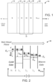
- FIG. 1 illustrates an example schematic illustration of a side-view of a cross-section of a superconductor thermal filter 10.
- the superconductor thermal filter 10 can be configured as a refrigeration stage employed in a cryogenic cooling application in which the superconductor thermal cooler is configured as a solid state device that is one of a plurality of solid state cooler devices placed around a refrigeration container that resides in a vacuum and holds superconducting circuitry.
- the plurality of solid state devices can provide the final stage in a cryogenic refrigeration system, and allow for efficient cooling by removal of heat from a cold side of the refrigeration stage, and prevent the return of heat from the hot side of the last refrigeration stage within a plurality of refrigeration stages.
- the superconductor thermal filter 10 can be employed as a connecting structure between two devices, such that the connecting structure is a multilayer connector or a bump bond structure.
- the superconductor thermal filter 10 is a NISN device with the superconductor portion being a multilayer superconductor structure 15.
- the superconductor thermal filter 10 includes a normal metal layer 12 disposed on a cold side of the superconductor thermal filter 10.
- the normal metal layer 12 is seperated from a first or cold side of the multilayer superconductor structure 15 by an insulator layer 14.
- a normal metal quasiparticle trap 22 is disposed on a second or hot side of the multilayer superconductor structure 15.
- the multilayer superconductor structure 15 includes a first superconductor layer 16 (S1) with a first energy bandgap, a second superconductor layer 18 (S2) with a second energy bandgap and a third superconductor layer (S3) with a third energy bandgap.
- the first energy bandgap is greater than the second energy bandgap, and the second energy bandgap is greather than the third energy bandgap.
- FIG. 2 illustrates a graph 34 that shows the principle of operation and the net heat flow of the superconductor thermal filter 10 of FIG. 1 , where hot electrons in the normal metal layer 12 above the Fermi level tunnel across the insulatator layer 14 into the first superconductor layer 16, thus removing heat from the normal metal layer 12.
- the hot electrons then move readily to the second superconductor layer 18 since it has a lower energy bandgap that the first supeconductor layer 16. These hot electrons then move readily to the third superconductor layer 20 since it has a lower energy bandgap that the second supeconductor layer 18. Finally, the hot electrons move into the normal metal quasiparticle trap 22 on the hot side of the superconductor thermal filter 10.
- the decreasing superconducting energy gaps reduces the quasiparticle backflow, while the use of a quasiparticle trap prevents the quasi particles from reintegrating into phonons while in the superconducting material.
- Each superconductor layer can be selected to have a thickness greater than 4 coherence lengths to ensure that the layers functions as a superconductor correctly.
- Each superconductor layer can also be selected to have a thermal boundary resistance mismatch between the interfaces of the superconductor layers.
- Each superconductor layer can be seleced to have a film layer thickness that is 1 ⁇ 4 wavelength (or a multiple) of its respective dominant phonon wavelenght based on its operating temperature. This allows for the superconductor structure to behave as a phonon filter where constructive interference at each layer minimizes the phonon heat flow.
- the normal metal layers can be formed of a normal metal such as from one of gold, titanium, chromium, platinum, or another metal that is above its superconducting transition temperature or a combination thereof.
- the superconductor material layers can be formed of indium, niobium, tin, molybdenum, titanium, aluminum, or some other superconducting metal.
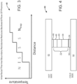
- FIG. 3 illustrates a graph 40 of temperature versus distance of the superconductor thermal filter 10 of FIG. 1 .
- the graph 40 illustrates the temperature increases through each layer of the NISN device.
- Each superconductor layer of the superconductor structure 15 is also selected to have a thermal boundary resistance mismatch between the interfaces of the superconductor layers. This provides for a well defined step function of temperature versus distance of the superconductor thermal filter 10 of FIG. 1 .
- FIG. 4 illustrates a schematic cross-sectional view of an example of a multichip superconductor structure 50 showing a single multilayer superconductor bump bond structure 70
- FIG. 5 shows the multichip superconducting structure 50 with a plurality of the single multilayer superconductor bump bond structures 70.
- the multichip superconducting structure 50 includes a first superconducting device 52 (e.g., bottom device or main device) connected to a second superconducting device 62 (e.g., top device or auxiliary device), through the plurality of multilayer superconductor bump bond structures 70.
- a multichip superconductor structure could include multiple superconductor devices connected to another superconductor device.
- a superconductor device can be a substrate wafer, a package device for passing signals to another device, an integrated circuit (IC), or a variety of other types of superconductor devices.
- IC integrated circuit
- the first superconductor device 52 includes a plurality of first normal metal contact pads 56 disposed at or near a top side of the first superconductor device 52.
- the second superconductor device 62 includes a plurality of second normal metal contact pads 66 disposed at or near a bottom side of the second superconductor device 62.
- the first superconductor device 52 is electrically and mechanically coupled to the second superconductor device 62 by the plurality of multilayer superconducting bump bond structures 70 that bond the devices to one another through corresponding normal metal contact pads of the first and second superconductor devices 52 and 62, respectively.
- An insulating layer 54 resides between each of the plurality of first normal metal contact pads 56 and the corresponding multilayer superconducting bump bond structure 70.
- the normal metal contact pads and the insulating layers are shown as residing above the superconducting devices, they could reside within the superconducting devices.
- Each multilayer superconducting bump bond structure 70 includes a first superconductor layer 58 with a first energy bandgap, a second superconductor layer 60 with a second energy bandgap and a third superconductor layer 68 with a third energy bandgap.
- the first energy bandgap is greater than the second energy bandgap, and the second energy bandgap is greather than the third energy bandgap.
- the plurality of first normal metal contact pads 56 reside on a cold side of the multichip superconductor structure 50, while the plurality of second normal metal contact pads 66 reside on a hot side of the multichip superconductor structure 50.
- the superconducting metal material of the first, second and third superconductor metal layers 20 are selected to provide a good thermal boundary resistance at each superconductor material layer interface to inhibit the flow of heat.
- the thickness of each metal layer can be selected to be greater than a thickness of at least 4 coherence lengths of the type of superconducting metal in the superconductor metal layer to assure that the superconductor metal layer retains its superconducting properties.
- Each superconductor layer can be seleced to have a film layer thickness that is 1 ⁇ 4 wavelength (or a multiple) of its respective dominant phonon wavelenght based on its operating temperature.
- FIG. 6 illustrates a schematic cross-sectional view of an example of a solid state cooler device 100 that employs a superconductor thermal filter.
- the solid state cooler device 100 can be configured as a refrigeration stage employed in a cryogenic cooling application in which the solid state structure is one of a plurality of solid state cooler devices disposed about a refrigeration container that resides in a vacuum and holds superconducting circuitry.
- the plurality of solid state structures can provide the final stage in a cryogenic refrigeration system, and allow for efficient cooling by removal of heat from a cold side of the refrigeration stage, and prevent the return of heat from the hot side of the last refrigeration stage within a plurality of refrigeration stages.
- the solid state cooler device can include a NIS junction or a NISN junction. The return of heat extracted from the cold side of the solid state cooler device is mitigated by employing a multilayer superconductor structure having superconductor layers of decreasing bandgaps from the cold side to the hot side.
- the solid state cooler device 100 includes a substrate 102 that is disposed on a hot side of a refrigeration stage.
- a first conductive pad 104 is disposed on the substrate 102, and a second conductive pad 106 is disposed on the substrate 102.
- the first conductive pad 104 is spaced apart from the second conductive pad 106 by a gap 108.
- a first multilayer superconductor structure 115 includes a first side (or cold side) configured to face the cold side of the refrigerator stage and a second side (or hot side) configured to face the hot side of the refrigeration stage.
- the second side of the first multilayer superconductor structure 115 is disposed on and in contact with the first conductive pad 104.
- a second multilayer superconductor structure 125 includes a first side facing the cold side of the refrigeration stage, and a second side facing the hot side of the refrigeration stage. The second side of the second multilayer superconductor structure 125 is disposed on and in contact with the second conductive pad 106.
- the first multilayer superconductor structure 115 includes a first superconductor layer 114 with a first energy bandgap, a second superconductor layer 112 with a second energy bandgap and a third superconductor layer 110 with a third energy bandgap.
- the first energy bandgap is greater than the second energy bandgap, and the second energy bandgap is greather than the third energy bandgap.
- the second multilayer superconductor structure 125 includes a fourth superconductor layer 124 with a fourth energy bandgap, a fifth superconductor layer 122 with a fifth energy bandgap and a sixth superconductor layer 120 with a sixth energy bandgap.
- the fourth energy bandgap is greater than the fifth energy bandgap, and the fifth energy bandgap is greather than the sixth energy bandgap.
- a first insulating layer 116 is disposed between a surface of the first side of first multilayer superconductor structure 115, and a first end of a normal metal layer 118, and a second insulating layer 128 is disposed between a surface of the first side of the second multilayer superconductor structure 125, and a second end of the normal metal layer 118.
- a bias voltage is applied between the first conductive pad 104 and the second conductive pad 106 to remove hot electrons from the normal metal layer 118. The bias voltage raises the energy level of the hot electrons on the normal metal layer 118.
- the first conductive pad 104 and the second conductive pad 106 can be formed from a normal metal or a superconducting metal.
- the first conductive pad 104 and the second conductive pad 106 act as a quasi-particle trap when formed of a normal metal.
- the normal metal layers can be formed of a normal metal such as from one of gold, titanium, chromium, platinum, or another metal that is above its superconducting transition temperature or a combination thereof.
- the superconductor material layers can be formed of indium, niobium, tin, molybdenum, titanium, aluminum, or some other superconducting metal.
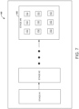
- FIG. 7 illustrates a block diagram of a refrigeration system 140 that employs solid state devices such as the solid state device 100 of FIG. 6 .
- the refrigeration system 140 includes a plurality of stages labeled stage #1 to stage #N, where N is an integer greater than or equal to 2.
- Each refrigeration stage provides an additional temperature drop from the previous stage, such that the Nth stage is the final stage and provides the last temperature drop and lowest temperature of the refrigeration system 140.
- the Nth stage is a first or intermediary stage as opposed to the last stage.
- Stage #N in the refrigeration system 140 includes a refrigeration container 150 with a plurality of solid state devices 152 similar to that illustrated in FIG. 6 disposed about the container and cooperating to provide the final lowest temperature of the refrigeration system 140 within the container 150.
- the container 150 can be in a vacuum environment and be configured to house superconducting circuitry.
- one or more of the other stages employ solid state devices similar to those in stage #N to provide incremental temperature drops across the refrigeration system 140.
- the refrigeration container 150 can be formed of a normal metal that provides the final normal metal layer of each solid state device 152.
- FIG. 8 illustrates an example of a method 200 for providing a superconductor thermal filter.
- a normal metal layer is provided having a first side and a second side.
- an insulating layer is disposed overlying the first side of the normal metal layer.
- a multilayer superconductor structure is disposed having a first side overlying a side of the insulting layer opposite the side that overlies the normal metal layer.
- the multilayer superconductor structure includes a plurality of superconductor layers with each superconductor layer having a smaller superconducting energy band gap than the preceding superconductor as the superconductor layers extend away from the normal metal layer.
- a normal metal layer quasiparticle trap is disposed with a first side disposed on a second side of the multilayer superconductor structure.
- a bias voltage is applied between the normal metal layer and the normal metal layer quasiparticle trap to remove hot electrons from the normal metal layer through each superconductor layer of the multilayer superconductor structure to the normal metal layer quasiparticle trap.
- overlay For purposes of simplification of explanation the terms “overlay”, “overlaying”, “underlay” and “underlying” (and derivatives) are employed throughout this disclosure to denote a relative position of two adjacent surfaces in a selected orientation. Additionally, the terms “top” and “bottom” employed throughout this disclosure denote opposing surfaces in the selected orientation. Similarly, the terms “upper” and “lower” denote relative positions in the selected orientation are for purposes of illustration. In fact, the examples used throughout this disclosure denote one selected orientation. In the described examples, however, the selected orientation is arbitrary and other orientations are possible (e.g., upside down, rotated by 90 degrees, etc.) within the scope of the present disclosure.
Landscapes
- Engineering & Computer Science (AREA)
- Physics & Mathematics (AREA)
- Mechanical Engineering (AREA)
- Thermal Sciences (AREA)
- General Engineering & Computer Science (AREA)
- Manufacturing & Machinery (AREA)
- Superconductor Devices And Manufacturing Methods Thereof (AREA)
Description
- The present invention relates generally to superconductors, and more particularly to a superconductor thermal filter.
- Solid-state electron cooling by the tunneling of "hot" electrons across a normal metal - insulator -superconductor (NIS) junction, using a bias voltage, has been proven to work below 1K, substantially operating like the more familiar near roomtemperature expensive Peltier thermo-electric refrigerator. These NIS cryo-coolers are built from the same materials as Josephson junctions used in the superconducting circuitry and by the same lithography fabrication foundry tools, and are fundamentally completely compatible with the Josephson junction components. They could be integrated alongside the Josephson junctions themselves, fabricated concurrently. However, currently NIS coolers have a very limited temperature throw, with a maximum temperature difference between hot and cold sides of ~150 mK.
- One of the main limitations to NIS coolers' full performance is the presence in the superconducting leads of non-equilibrium quasi-particles arising from the high current running through the device. The low quasi-particle relaxation rate and thermal conductivity in a superconductor bind these hot particles in the vicinity of the junction and lead to severe overheating in the superconducting electrodes. There are several methods for reducing the accumulation of quasi-particles in a superconductor. The most common method is to use a normal metal coupled to the superconductor referred to as a quasiparticle trap, such that quasi-particles migrate to the normal metal and relax their energy there through electron-electron and electron-phonon interaction. This device is referred to as a normal metal - insulator -superconductor - normal metal (NISN) junction. However, phonon heat generated in the quasiparticle trap can migrate back to the superconducting electrodes also limiting the temperature difference between the hot side and cold sides of the NISN junction solid state cooler. Known devices are described in H. Courtois et al., "High-performance electronic cooling with superconducting tunnel junctions", Comptes Rendus Physique, vol. 17, p. 1139-1145, (2016); H.Q. Nguyen et al., "A robust platform cooled by superconducting electronic refrigerators", Applied Physics Letters, vol. 106, 012601, p. 1-5, (2015); H.Q. Nguyen et al., "A cascade electronic refrigerator using superconducting tunnel junctions", arXiv:1605.00830v1 [cond-mat.mes-hall], p. 1-7, (2016); Ian Jasper Agulo et al., "Effective electron microrefrigeration by superconductor-insulator-normal metal tunnel junctions with advanced geometry of electrodes and normal metal traps", Nanotechnology, vol. 15, p. S224-S228, (2004);
US 6 581 387 B1 ; M. Camarasa-Gómez et al., "Superconducting cascade electron refrigerator", Applied Physics Letters, vol. 104, 192601, p. 1-5, (2014). - In one example, a superconductor thermal filter is provided that includes a normal metal layer having a first side and a second side, an insulating layer overlying the first side of the normal metal layer, and a multilayer superconductor structure having a first side overlying a side of the insulting layer opposite the side that overlies the normal metal layer. The multilayer superconductor structure comprises a plurality of superconductor layers with each superconductor layer having a smaller superconducting energy band gap than the preceding superconductor as the superconductor layers extend away from the normal metal layer. The superconductor thermal filter further comprises a normal metal layer quasiparticle trap having a first side and a second side with the first side being disposed on a second side of the multilayer superconductor structure. A bias voltage is applied between the normal metal layer and the normal metal layer quasiparticle trap to remove hot electrons from the normal metal layer through each superconductor layer of the multilayer superconductor structure to the normal metal layer quasiparticle trap.
- In another example, a method is disclosed of forming a superconductor thermal filter. The method comprises providing a normal metal layer having a first side and a second side, disposing an insulating layer overlying the first side of the normal metal layer, and disposing a multilayer superconductor structure having a first side overlying a side of the insulting layer opposite the side that overlies the normal metal layer. The multilayer superconductor structure comprises a plurality of superconductor layers with each superconductor layer having a smaller superconducting energy band gap than the preceding superconductor as the superconductor layers extend away from the normal metal layer. The method further comprises disposing a normal metal layer quasiparticle trap with a first side and a second side with the first side being disposed on a second side of the multilayer superconductor structure.
-
-
FIG. 1 illustrates an example schematic illustration of a side-view of a cross-section of a superconductor thermal filter. -
FIG. 2 illustrates a graph that shows the principle of operation and the net heat flow of the superconductor thermal filter ofFIG. 1 -
FIG. 3 illustrates a graph of temperature versus distance of the superconductor thermal filter ofFIG. 1 . -
FIG. 4 illustrates a schematic cross-sectional view of an example of a multichip superconductor structure showing a single multilayer superconductor bump bond structure. -
FIG. 5 illustrates a schematic cross-sectional view of the multichip superconducting structure ofFIG. 4 with a plurality of the single multilayer superconductor bump bond structures. -
FIG. 6 illustrates a schematic cross-sectional view of an example of a solid state cooler device that employs a superconductor thermal filter. -
FIG. 7 illustrates a block diagram of a refrigeration system that employs solid state devices such as the solid state device ofFIG. 6 . -
FIG. 8 illustrates a method of forming a superconductor thermal filter. - The disclosure relates to a superconductor thermal filter composed of a plurality of layers of individual superconducting materials. Each superconductor layer has a smaller superconducting energy band gap than the preceding material when moving from a cold temperature side to a hot temperature side. The effect of this is that as "hot" electrons (quasiparticles) progress from one layer to another they will fall into each material with a smaller energy band gap and be unable to travel back into the larger energy band gap material. The superconductor thermal filter can be can be a normal metal - insulator -superconductor (NIS) junction device or a normal metal - insulator -superconductor- normal metal (NISN) junction device in which the superconductor portion is formed from a plurality of different superconductor layers with decreasing energy band gaps from a cold temperature side to a hot temperature side. A normal metal is a metal that does not superconduct at cryogenic operating temperatures. This superconductor thermal filter functions as a band gap filter and also serves to prevent the backwards flow of quasi particles, and phonons.
- In one example, a "hot" electron and phonon filter for use with a NISN junction is disclosed. The filter is formed from a plurality of layers of superconducting material preventing the backward flow of "hot" electrons and phonons from the normal metal trap into the NIS junction. In the current state of the art there is nothing to prevent the backwards flow of quasi-particle (unpaired electron like particles in a superconductor) from a quasi-particle trap back into the superconductor. Furthermore, there is only a single thermal boundary resistance to prevent the flow of phonons passing into the superconductor. In the present examples, a plurality of superconducting material layers provide a strong bandgap thermal filter by providing multiple bandgaps that the hot electrons and interfacial thermal boundary resistance that the hot phonons need to overcome to return heat to the normal metal layer on the cold side of the superconductor thermal filter.
- Phonons are quantized lattice vibrations that carry the heat in superconductors, and partially carry heat in normal metals. Normal metals will also carry heat by electrons. Each time the heat encounters a superconductor layer, the heat primarily is carried by phonons as vibrations. The vibrations have a dominant wavelength based on the specific material and its current temperature.
- Superconductors can proximitize each other. Therefore a thickness greater than 4 coherence lengths is desired to ensure that the layers function correctly. There is also a thermal boundary resistance mismatch between the superconductors. This will be tuned to block the dominant phonon wavelength which will prevent phonons from the "hot" electron trap from flowing into the NIS Junction. The dominant phonon wavelength is an approximation that at any temperature the heat is predominately carried by a single frequency vmax of the phonon vibrations. The dominant phonon wavelength is then found as λdom= v/ vmax where v is the speed of sound. Similar to optical fibers, by choosing film layer thicknesses that are ¼ wavelength (or a multiple), a phonon filter can be setup where constructive interference at each layer minimizes the phonon heat flow.
- Thermal boundary resistance, or Kapitza resistance, is a measure of an interface's resistance to thermal flow. Owing to differences in electronic and vibrational properties in different materials, when an energy carrier (phonon or electron, depending on the material) attempts to traverse the interface, it will scatter at the interface. The probability of transmission after scattering will depend on the available energy states on
side 1 andside 2 of the interface. - In one example, the superconductor thermal filter can be employed to separate circuitry residing on different superconducting structures in a multi-chip device. The superconductor thermal filter can be a bump bond structure or part of a bump bond structure that also bonds two chips together in a multi-chip device. In another example, the superconductor thermal filter can be employed in a solid state cooler device that can be employed in a refrigeration system. The solid state cooler devices can form a last refrigeration stage in a plurality of refrigeration stages to provide cooling down to milliKelvin temperatures. The solid state cooler can be a NIS or a NISN device.
-
FIG. 1 illustrates an example schematic illustration of a side-view of a cross-section of a superconductorthermal filter 10. The superconductorthermal filter 10 can be configured as a refrigeration stage employed in a cryogenic cooling application in which the superconductor thermal cooler is configured as a solid state device that is one of a plurality of solid state cooler devices placed around a refrigeration container that resides in a vacuum and holds superconducting circuitry. The plurality of solid state devices can provide the final stage in a cryogenic refrigeration system, and allow for efficient cooling by removal of heat from a cold side of the refrigeration stage, and prevent the return of heat from the hot side of the last refrigeration stage within a plurality of refrigeration stages. Alternatively, the superconductorthermal filter 10 can be employed as a connecting structure between two devices, such that the connecting structure is a multilayer connector or a bump bond structure. - The superconductor
thermal filter 10 is a NISN device with the superconductor portion being amultilayer superconductor structure 15. The superconductorthermal filter 10 includes anormal metal layer 12 disposed on a cold side of the superconductorthermal filter 10. Thenormal metal layer 12 is seperated from a first or cold side of themultilayer superconductor structure 15 by aninsulator layer 14. A normalmetal quasiparticle trap 22 is disposed on a second or hot side of themultilayer superconductor structure 15. Themultilayer superconductor structure 15 includes a first superconductor layer 16 (S1) with a first energy bandgap, a second superconductor layer 18 (S2) with a second energy bandgap and a third superconductor layer (S3) with a third energy bandgap. The first energy bandgap is greater than the second energy bandgap, and the second energy bandgap is greather than the third energy bandgap. - A bias voltage (+V/-V) is applied between the
normal metal layer 12 disposed on the cold side of the superconductorthermal filter 10 and the normalmetal quasiparticle trap 22 disposed on the hot side of the superconductorthermal filter 10. The bias voltage (V+/ -V) raises the energy level of the hot electrons on thenormal metal layer 12.FIG. 2 illustrates a graph 34 that shows the principle of operation and the net heat flow of the superconductorthermal filter 10 ofFIG. 1 , where hot electrons in thenormal metal layer 12 above the Fermi level tunnel across theinsulatator layer 14 into thefirst superconductor layer 16, thus removing heat from thenormal metal layer 12. The hot electrons then move readily to thesecond superconductor layer 18 since it has a lower energy bandgap that thefirst supeconductor layer 16. These hot electrons then move readily to thethird superconductor layer 20 since it has a lower energy bandgap that thesecond supeconductor layer 18. Finally, the hot electrons move into the normalmetal quasiparticle trap 22 on the hot side of the superconductorthermal filter 10. The decreasing superconducting energy gaps reduces the quasiparticle backflow, while the use of a quasiparticle trap prevents the quasi particles from reintegrating into phonons while in the superconducting material. - In one example, the
first superconductor layer 16 is formed of niobium (Nb) with a superconducting energy bandgap of 2Δ=30.5 × 10⁻⁴ eV, thesecond superconductor layer 18 is formed of tin (Sn) with a superconducting energy bandgap of 2Δ=11.5 × 10⁻⁴ eV, and thethird superconductor layer 20 is formed of aluminum (Al) with a superconducting energy bandgap of 2Δ=3.4 × 10⁻⁴ eV. In yet another example, thefirst superconductor layer 16 is formed of aluminum (Al) with a superconducting energy bandgap of 2Δ=3.4 × 10⁻⁴ eV, thesecond superconductor layer 18 is formed of molybdenum (Mo) with a superconducting energy bandgap of 2Δ=2.7 × 10⁻⁴ eV, and thethird superconductor layer 20 is formed of titanium (Ti) with a superconducting energy bandgap of 2Δ=1.2 × 10⁻⁴ eV. It is to be appreciated that a variety of different superconducting material layers and a different number of superconducting material layers could be employed as long as they are selected to having progressinginly decreasing superconducting energy bandgaps from thenormal metal layer 12 to the normal metallayer quasiparticle trap 22. - Each superconductor layer can be selected to have a thickness greater than 4 coherence lengths to ensure that the layers functions as a superconductor correctly. Each superconductor layer can also be selected to have a thermal boundary resistance mismatch between the interfaces of the superconductor layers. Each superconductor layer can be seleced to have a film layer thickness that is ¼ wavelength (or a multiple) of its respective dominant phonon wavelenght based on its operating temperature. This allows for the superconductor structure to behave as a phonon filter where constructive interference at each layer minimizes the phonon heat flow. The normal metal layers can be formed of a normal metal such as from one of gold, titanium, chromium, platinum, or another metal that is above its superconducting transition temperature or a combination thereof. The superconductor material layers can be formed of indium, niobium, tin, molybdenum, titanium, aluminum, or some other superconducting metal.
-
FIG. 3 illustrates agraph 40 of temperature versus distance of the superconductorthermal filter 10 ofFIG. 1 . Thegraph 40 illustrates the temperature increases through each layer of the NISN device. Each superconductor layer of thesuperconductor structure 15 is also selected to have a thermal boundary resistance mismatch between the interfaces of the superconductor layers. This provides for a well defined step function of temperature versus distance of the superconductorthermal filter 10 ofFIG. 1 . -
FIG. 4 illustrates a schematic cross-sectional view of an example of amultichip superconductor structure 50 showing a single multilayer superconductorbump bond structure 70, whileFIG. 5 shows the multichipsuperconducting structure 50 with a plurality of the single multilayer superconductorbump bond structures 70. The multichipsuperconducting structure 50 includes a first superconducting device 52 (e.g., bottom device or main device) connected to a second superconducting device 62 (e.g., top device or auxiliary device), through the plurality of multilayer superconductorbump bond structures 70. A multichip superconductor structure could include multiple superconductor devices connected to another superconductor device. A superconductor device can be a substrate wafer, a package device for passing signals to another device, an integrated circuit (IC), or a variety of other types of superconductor devices. - The
first superconductor device 52 includes a plurality of first normalmetal contact pads 56 disposed at or near a top side of thefirst superconductor device 52. Thesecond superconductor device 62 includes a plurality of second normalmetal contact pads 66 disposed at or near a bottom side of thesecond superconductor device 62. Thefirst superconductor device 52 is electrically and mechanically coupled to thesecond superconductor device 62 by the plurality of multilayer superconductingbump bond structures 70 that bond the devices to one another through corresponding normal metal contact pads of the first andsecond superconductor devices layer 54 resides between each of the plurality of first normalmetal contact pads 56 and the corresponding multilayer superconductingbump bond structure 70. The multilayer superconductingbump bond structure 70 along with the insulatinglayer 54 and the normalmetal contact pads device 50. Although, the normal metal contact pads and the insulating layers are shown as residing above the superconducting devices, they could reside within the superconducting devices. - Each multilayer superconducting
bump bond structure 70 includes afirst superconductor layer 58 with a first energy bandgap, asecond superconductor layer 60 with a second energy bandgap and athird superconductor layer 68 with a third energy bandgap. The first energy bandgap is greater than the second energy bandgap, and the second energy bandgap is greather than the third energy bandgap. The plurality of first normalmetal contact pads 56 reside on a cold side of themultichip superconductor structure 50, while the plurality of second normalmetal contact pads 66 reside on a hot side of themultichip superconductor structure 50. Furthermore, the superconducting metal material of the first, second and thirdsuperconductor metal layers 20 are selected to provide a good thermal boundary resistance at each superconductor material layer interface to inhibit the flow of heat. The thickness of each metal layer can be selected to be greater than a thickness of at least 4 coherence lengths of the type of superconducting metal in the superconductor metal layer to assure that the superconductor metal layer retains its superconducting properties. Each superconductor layer can be seleced to have a film layer thickness that is ¼ wavelength (or a multiple) of its respective dominant phonon wavelenght based on its operating temperature. -
FIG. 6 illustrates a schematic cross-sectional view of an example of a solid statecooler device 100 that employs a superconductor thermal filter. The solid statecooler device 100 can be configured as a refrigeration stage employed in a cryogenic cooling application in which the solid state structure is one of a plurality of solid state cooler devices disposed about a refrigeration container that resides in a vacuum and holds superconducting circuitry. The plurality of solid state structures can provide the final stage in a cryogenic refrigeration system, and allow for efficient cooling by removal of heat from a cold side of the refrigeration stage, and prevent the return of heat from the hot side of the last refrigeration stage within a plurality of refrigeration stages. The solid state cooler device can include a NIS junction or a NISN junction. The return of heat extracted from the cold side of the solid state cooler device is mitigated by employing a multilayer superconductor structure having superconductor layers of decreasing bandgaps from the cold side to the hot side. - As illustrated in
FIG. 6 , the solid statecooler device 100 includes asubstrate 102 that is disposed on a hot side of a refrigeration stage. A firstconductive pad 104 is disposed on thesubstrate 102, and a secondconductive pad 106 is disposed on thesubstrate 102. The firstconductive pad 104 is spaced apart from the secondconductive pad 106 by agap 108. A firstmultilayer superconductor structure 115 includes a first side (or cold side) configured to face the cold side of the refrigerator stage and a second side (or hot side) configured to face the hot side of the refrigeration stage. The second side of the firstmultilayer superconductor structure 115 is disposed on and in contact with the firstconductive pad 104. A secondmultilayer superconductor structure 125 includes a first side facing the cold side of the refrigeration stage, and a second side facing the hot side of the refrigeration stage. The second side of the secondmultilayer superconductor structure 125 is disposed on and in contact with the secondconductive pad 106. - The first
multilayer superconductor structure 115 includes afirst superconductor layer 114 with a first energy bandgap, asecond superconductor layer 112 with a second energy bandgap and athird superconductor layer 110 with a third energy bandgap. The first energy bandgap is greater than the second energy bandgap, and the second energy bandgap is greather than the third energy bandgap. The secondmultilayer superconductor structure 125 includes afourth superconductor layer 124 with a fourth energy bandgap, afifth superconductor layer 122 with a fifth energy bandgap and asixth superconductor layer 120 with a sixth energy bandgap. The fourth energy bandgap is greater than the fifth energy bandgap, and the fifth energy bandgap is greather than the sixth energy bandgap. - A first insulating
layer 116 is disposed between a surface of the first side of firstmultilayer superconductor structure 115, and a first end of anormal metal layer 118, and a second insulatinglayer 128 is disposed between a surface of the first side of the secondmultilayer superconductor structure 125, and a second end of thenormal metal layer 118. A bias voltage is applied between the firstconductive pad 104 and the secondconductive pad 106 to remove hot electrons from thenormal metal layer 118. The bias voltage raises the energy level of the hot electrons on thenormal metal layer 118. The firstconductive pad 104 and the secondconductive pad 106 can be formed from a normal metal or a superconducting metal. The firstconductive pad 104 and the secondconductive pad 106 act as a quasi-particle trap when formed of a normal metal. - The normal metal layers can be formed of a normal metal such as from one of gold, titanium, chromium, platinum, or another metal that is above its superconducting transition temperature or a combination thereof. The superconductor material layers can be formed of indium, niobium, tin, molybdenum, titanium, aluminum, or some other superconducting metal.
-
FIG. 7 illustrates a block diagram of arefrigeration system 140 that employs solid state devices such as thesolid state device 100 ofFIG. 6 . Therefrigeration system 140 includes a plurality of stages labeledstage # 1 to stage #N, where N is an integer greater than or equal to 2. Each refrigeration stage provides an additional temperature drop from the previous stage, such that the Nth stage is the final stage and provides the last temperature drop and lowest temperature of therefrigeration system 140. In other examples, the Nth stage is a first or intermediary stage as opposed to the last stage. Stage #N in therefrigeration system 140 includes arefrigeration container 150 with a plurality ofsolid state devices 152 similar to that illustrated inFIG. 6 disposed about the container and cooperating to provide the final lowest temperature of therefrigeration system 140 within thecontainer 150. Thecontainer 150 can be in a vacuum environment and be configured to house superconducting circuitry. In another example, one or more of the other stages employ solid state devices similar to those in stage #N to provide incremental temperature drops across therefrigeration system 140. In other examples, therefrigeration container 150 can be formed of a normal metal that provides the final normal metal layer of eachsolid state device 152. -
FIG. 8 illustrates an example of amethod 200 for providing a superconductor thermal filter. At 210, a normal metal layer is provided having a first side and a second side. At 220, an insulating layer is disposed overlying the first side of the normal metal layer. At 230, a multilayer superconductor structure is disposed having a first side overlying a side of the insulting layer opposite the side that overlies the normal metal layer. The multilayer superconductor structure includes a plurality of superconductor layers with each superconductor layer having a smaller superconducting energy band gap than the preceding superconductor as the superconductor layers extend away from the normal metal layer. At 240, a normal metal layer quasiparticle trap is disposed with a first side disposed on a second side of the multilayer superconductor structure. Next, at 250, a bias voltage is applied between the normal metal layer and the normal metal layer quasiparticle trap to remove hot electrons from the normal metal layer through each superconductor layer of the multilayer superconductor structure to the normal metal layer quasiparticle trap. - For purposes of simplification of explanation the terms "overlay", "overlaying", "underlay" and "underlying" (and derivatives) are employed throughout this disclosure to denote a relative position of two adjacent surfaces in a selected orientation. Additionally, the terms "top" and "bottom" employed throughout this disclosure denote opposing surfaces in the selected orientation. Similarly, the terms "upper" and "lower" denote relative positions in the selected orientation are for purposes of illustration. In fact, the examples used throughout this disclosure denote one selected orientation. In the described examples, however, the selected orientation is arbitrary and other orientations are possible (e.g., upside down, rotated by 90 degrees, etc.) within the scope of the present disclosure.
- Described above are examples of the subject disclosure. It is, of course, not possible to describe every conceivable combination of components or methodologies for purposes of describing the subject disclosure, but one of ordinary skill in the art may recognize that many further combinations and permutations of the subject disclosure are possible. Accordingly, the subject disclosure is intended to embrace all such alterations, modifications and variations that fall within the invention as defined by the claims. In addition, where the disclosure or claims recite "a," "an," "a first," or "another" element, or the equivalent thereof, it should be interpreted to include one or more than one such element, neither requiring nor excluding two or more such elements. Furthermore, to the extent that the term "includes" is used in either the detailed description or the claims, such term is intended to be inclusive in a manner similar to the term "comprising" as "comprising" is interpreted when employed as a transitional word in a claim. Finally, the term "based on" is interpreted to mean at least based in part.
Claims (15)
- A superconductor thermal filter (10) comprising:a normal metal layer (12) having a first side and a second side;an insulating layer (14) overlying the first side of the normal metal layera multilayer superconductor structure having a first side overlying a side of the insulating layer opposite the side that overlies the normal metal layer, anda normal metal layer quasiparticle trap (22) having a first side and a second side, the first side being disposed on a second side of the multilayer superconductor structure;wherein a bias voltage is applicable between the normal metal layer and the normal metal layer quasiparticle trap to remove hot electrons from the normal metal layer through each superconductor layer of the multilayer superconductor structure to the normal metal layer quasiparticle trap,characterised by the multilayer superconductor structure comprised of a plurality of superconductor layers (16, 18, 20) with each superconductor layer having a smaller superconducting energy band gap than the preceding superconductor layer extending away from the normal metal layer.
- The superconductor thermal filter (10) of claim 1, wherein the multilayer superconductor structure comprises a first superconductor layer (16) with a first energy bandgap, a second superconductor layer (18) with a second energy bandgap and a third superconductor layer (20) with a third energy bandgap, such that the first energy bandgap is greater than the second energy bandgap, and the second energy bandgap is greater than the third energy bandgap.
- The superconductor thermal filter (10) of claim 2, wherein the first superconductor layer (16) is formed of niobium, Nb, with a superconducting energy bandgap of 2Δ=30.5 × 10⁻⁴ eV, the second superconductor layer (18) is formed of tin, Sn, with a superconducting energy bandgap of 2Δ=11.5 × 10⁻⁴ eV, and the third superconductor layer (20) is formed of aluminum, Al with a superconducting energy bandgap of 2Δ=3.4 × 10⁻⁴ eV.
- The superconductor thermal filter (10) of claim 2, wherein the first superconductor layer (16) is formed of aluminum, Al, with a superconducting energy bandgap of 2Δ=3.4 × 10⁻⁴ eV, the second superconductor layer (18) is formed of molybdenum, Mo, with a superconducting energy bandgap of 2Δ=2.7 × 10⁻⁴ eV, and the third superconductor layer (20) is formed of titanium, Ti, with a superconducting energy bandgap of 2Δ=1.2 × 10⁻⁴ eV.
- The superconductor thermal filter (10) of claim 1, wherein each of the plurality of superconductor layers has a thickness thicker than 4 coherence lengths associated with the respective superconductor of the respective superconductor layer.
- The superconductor thermal filter (10) of claim 1, wherein each of the plurality of superconductor layers is selected to have a thermal boundary resistance mismatch between the interfaces of adjoining superconductor layers.
- The superconductor thermal filter (10) of claim 1, wherein at least one of the plurality of superconducting layers has a film layer thickness that is ¼ wavelength or a multiple of a ¼ wavelength of the dominant phonon associated with the operating temperature of the respective superconductor layer.
- A solid state cooler (100) comprising the superconductor thermal filter (10) as claimed in claim 1.
- A multichip device (50) comprising a first device (52) coupled to a second device (62) by at least a portion of the superconductor thermal filter (10) as claimed in claim 1
- A refrigeration system (140) comprising a plurality of refrigeration stages, wherein at least one stage of the refrigeration system comprises a refrigeration container (150) and a plurality of superconductor thermal filters (152) as claimed in claim 1 disposed about the refrigeration container.
- The superconductor thermal filter (10) of claim 1, wherein exposing the second side of the normal metal layer quasiparticle trap to a first environment at a first temperature holds a second environment on the second side of the normal metal layer to a second temperature that is less than the first temperature.
- A method (200) of forming a superconductor thermal filter (10), the method comprising:providing (210) a normal metal layer (12) having a first side and a second sidedisposing (220) an insulating layer (14) overlying the first side of the normal metal layerdisposing (230) a multilayer superconductor structure having a first side overlying a side of the insulating layer opposite the side that overlies the normal metal layer, the multilayer superconductor structure comprised of a plurality of superconductor layers (16, 18, 20); anddisposing (240) a normal metal layer quasiparticle trap (22) 2. with a first side and a second side, the first side being disposed on a second side of the multilayer superconductor structure,characterised by each superconductor layer having a smaller superconducting energy band gap than the preceding superconductor layer as the superconductor layers extend away from the normal metal layer.
- The method (200) of claim 12, further comprising applying (250) a bias voltage between the normal metal layer (12) and the normal metal layer quasiparticle trap (22) to remove hot electrons from the normal metal layer through each superconductor layer (16, 18, 20) of the multilayer superconductor structure to the normal metal layer quasiparticle trap.
- The method (200) of claim 12, wherein the multilayer superconductor structure comprises a first superconductor layer (16) with a first energy bandgap, a second superconductor layer (18) with a second energy bandgap and a third superconductor layer (20) with a third energy bandgap, such that the first energy bandgap is greater than the second energy bandgap, and the second energy bandgap is greather than the third energy bandgap.
- The method (200) of claim 14, wherein one of:the first superconductor layer (16) is formed of niobium, Nb, with a superconducting energy bandgap of 2Δ=30.5 × 10⁻⁴ eV, the second superconductor layer (18) is formed of tin, Sn, with a superconducting energy bandgap of 2Δ=11.5 × 10⁻⁴ eV, and the third superconductor layer (20) is formed of aluminum, Al, with a superconducting energy bandgap of 2Δ=3.4 × 10⁻⁴ eV; andthe first superconductor layer (16) is formed of aluminum, Al, with a superconducting energy bandgap of 2Δ=3.4 × 10⁻⁴ eV, the second superconductor layer (18) is formed of molybdenum, Mo, with a superconducting energy bandgap of 2Δ=2.7 × 10⁻⁴ eV, and the third superconductor layer (20) is formed of titanium, Ti, with a superconducting energy bandgap of 2Δ=1.2 × 10⁻⁴ eV.
Applications Claiming Priority (2)
| Application Number | Priority Date | Filing Date | Title |
|---|---|---|---|
| US16/554,155 US11189773B2 (en) | 2019-08-28 | 2019-08-28 | Superconductor thermal filter |
| PCT/US2020/043394 WO2021040923A1 (en) | 2019-08-28 | 2020-07-24 | Superconductor thermal filter |
Publications (2)
| Publication Number | Publication Date |
|---|---|
| EP4022690A1 EP4022690A1 (en) | 2022-07-06 |
| EP4022690B1 true EP4022690B1 (en) | 2023-11-15 |
Family
ID=72039698
Family Applications (1)
| Application Number | Title | Priority Date | Filing Date |
|---|---|---|---|
| EP20754110.3A Active EP4022690B1 (en) | 2019-08-28 | 2020-07-24 | Superconductor thermal filter |
Country Status (3)
| Country | Link |
|---|---|
| US (1) | US11189773B2 (en) |
| EP (1) | EP4022690B1 (en) |
| WO (1) | WO2021040923A1 (en) |
Families Citing this family (9)
| Publication number | Priority date | Publication date | Assignee | Title |
|---|---|---|---|---|
| US11333413B2 (en) | 2019-08-28 | 2022-05-17 | Northrop Grumman Systems Corporation | Solid state cooler device |
| US11302857B2 (en) * | 2019-11-19 | 2022-04-12 | International Business Machines Corporation | Cryogenic refrigeration for low temperature devices |
| US11211542B2 (en) * | 2019-11-19 | 2021-12-28 | International Business Machines Corporation | Cryogenic refrigeration for low temperature devices |
| US11600760B2 (en) | 2019-11-26 | 2023-03-07 | Northrop Grumman Systems Corporation | Cooler device with aluminum oxide insulators |
| US20210280763A1 (en) * | 2019-12-23 | 2021-09-09 | Microsoft Technology Licensing, Llc | Superconductor heterostructures for semiconductor-superconductor hybrid structures |
| US10998485B1 (en) | 2020-01-13 | 2021-05-04 | Northrop Grumman Systems Corporation | Cooler device with superconductor shunts |
| US11950510B2 (en) * | 2022-02-03 | 2024-04-02 | Northrop Grumman Systems Corporation | Superconductor junction for a solid state cooler |
| US20260036345A1 (en) * | 2023-08-01 | 2026-02-05 | Northrop Grumman Systems Corporation | Solid-State Cooler Device with Normal Metal Substrates |
| US12426504B2 (en) * | 2023-08-01 | 2025-09-23 | Northrop Grumman Systems Corporation | Solid-state cooler device with grid point contacts |
Family Cites Families (6)
| Publication number | Priority date | Publication date | Assignee | Title |
|---|---|---|---|---|
| JP3980682B2 (en) | 1996-07-22 | 2007-09-26 | 三洋電機株式会社 | Method for forming oxide superconducting device |
| FI964700A0 (en) * | 1996-11-26 | 1996-11-26 | Jukka Pekola | Mikroavkylningsapparat |
| US6581387B1 (en) | 2001-02-12 | 2003-06-24 | The United States Of America As Represented By The United States Department Of Energy | Solid-state microrefrigerator |
| US8301214B1 (en) | 2010-01-08 | 2012-10-30 | Hypres, Inc. | System and method for providing multi-conductive layer metallic interconnects for superconducting integrated circuits |
| FI20165492A (en) | 2015-12-29 | 2017-06-30 | Aalto-Korkeakoulusäätiö (Aalto Univ Foundation) | Circuit set, system and method for cooling electric quantum devices |
| US11333413B2 (en) | 2019-08-28 | 2022-05-17 | Northrop Grumman Systems Corporation | Solid state cooler device |
-
2019
- 2019-08-28 US US16/554,155 patent/US11189773B2/en active Active
-
2020
- 2020-07-24 WO PCT/US2020/043394 patent/WO2021040923A1/en not_active Ceased
- 2020-07-24 EP EP20754110.3A patent/EP4022690B1/en active Active
Also Published As
| Publication number | Publication date |
|---|---|
| EP4022690A1 (en) | 2022-07-06 |
| US11189773B2 (en) | 2021-11-30 |
| WO2021040923A1 (en) | 2021-03-04 |
| US20210066571A1 (en) | 2021-03-04 |
Similar Documents
| Publication | Publication Date | Title |
|---|---|---|
| US11189773B2 (en) | Superconductor thermal filter | |
| EP4022691B1 (en) | Solid state cooler device | |
| EP4066286B1 (en) | Cooler device with aluminum oxide insulators | |
| US20050150535A1 (en) | Method for forming a thin-film thermoelectric device including a phonon-blocking thermal conductor | |
| EP4091205B1 (en) | Cooler device with superconductor shunts and method of fabrication of the cooler device | |
| Van Duzer | Superconductor—semiconductor hybrid devices, circuits and systems | |
| EP4298874A1 (en) | A thermalization arrangement at cryogenic temperatures | |
| US11950510B2 (en) | Superconductor junction for a solid state cooler | |
| Van Duzer et al. | Semiconductor-superconductor hybrid electronics | |
| US12426504B2 (en) | Solid-state cooler device with grid point contacts | |
| US20260036345A1 (en) | Solid-State Cooler Device with Normal Metal Substrates | |
| Silver et al. | Applications of high temperature superconductors | |
| Bose et al. | An explanation for the rise in Tc in the Tl and Bi-based high-temperature superconductors | |
| WO2025158106A1 (en) | Indium attached bumps | |
| Shibani et al. | Electronic Specific Heat of Multi Levels Superconductors Based on the BCS Theory | |
| Priyanka et al. | Mechanism of superconductivity. | |
| Ullom et al. | A new idea for a solid-state microrefrigerator operating near 100 mK | |
| Shunmugavel | Rapid single flux quantum logic in high temperature superconductor technology | |
| JPH0284780A (en) | semiconductor equipment |
Legal Events
| Date | Code | Title | Description |
|---|---|---|---|
| STAA | Information on the status of an ep patent application or granted ep patent |
Free format text: STATUS: UNKNOWN |
|
| STAA | Information on the status of an ep patent application or granted ep patent |
Free format text: STATUS: THE INTERNATIONAL PUBLICATION HAS BEEN MADE |
|
| PUAI | Public reference made under article 153(3) epc to a published international application that has entered the european phase |
Free format text: ORIGINAL CODE: 0009012 |
|
| STAA | Information on the status of an ep patent application or granted ep patent |
Free format text: STATUS: REQUEST FOR EXAMINATION WAS MADE |
|
| 17P | Request for examination filed |
Effective date: 20220128 |
|
| AK | Designated contracting states |
Kind code of ref document: A1 Designated state(s): AL AT BE BG CH CY CZ DE DK EE ES FI FR GB GR HR HU IE IS IT LI LT LU LV MC MK MT NL NO PL PT RO RS SE SI SK SM TR |
|
| DAV | Request for validation of the european patent (deleted) | ||
| DAX | Request for extension of the european patent (deleted) | ||
| REG | Reference to a national code |
Ref country code: DE Ref legal event code: R079 Free format text: PREVIOUS MAIN CLASS: H01L0039220000 Ipc: B82Y0099000000 Ref country code: DE Ref legal event code: R079 Ref document number: 602020021153 Country of ref document: DE Free format text: PREVIOUS MAIN CLASS: H01L0039220000 Ipc: B82Y0099000000 |
|
| REG | Reference to a national code |
Ref country code: DE Ref legal event code: R079 Free format text: PREVIOUS MAIN CLASS: B82Y0099000000 Ipc: H01L0023340000 Ref document number: 602020021153 Country of ref document: DE |
|
| RIC1 | Information provided on ipc code assigned before grant |
Ipc: H10N 60/01 20230101ALI20230315BHEP Ipc: H10N 60/10 20230101ALI20230315BHEP Ipc: H01L 23/00 20060101ALI20230315BHEP Ipc: H01L 23/373 20060101ALI20230315BHEP Ipc: F25B 21/00 20060101ALI20230315BHEP Ipc: B82Y 99/00 20110101AFI20230315BHEP |
|
| RIC1 | Information provided on ipc code assigned before grant |
Ipc: H01L 23/00 20060101ALN20230330BHEP Ipc: H10N 60/01 20230101ALI20230330BHEP Ipc: H10N 60/10 20230101ALI20230330BHEP Ipc: H01L 23/373 20060101ALI20230330BHEP Ipc: F25B 21/00 20060101ALI20230330BHEP Ipc: B82Y 99/00 20110101ALI20230330BHEP Ipc: H01L 23/34 20060101AFI20230330BHEP |
|
| RIC1 | Information provided on ipc code assigned before grant |
Ipc: H01L 23/00 20060101ALN20230331BHEP Ipc: H10N 60/01 20230101ALI20230331BHEP Ipc: H10N 60/10 20230101ALI20230331BHEP Ipc: H01L 23/373 20060101ALI20230331BHEP Ipc: F25B 21/00 20060101ALI20230331BHEP Ipc: B82Y 99/00 20110101ALI20230331BHEP Ipc: H01L 23/34 20060101AFI20230331BHEP |
|
| RIC1 | Information provided on ipc code assigned before grant |
Ipc: H01L 23/00 20060101ALN20230418BHEP Ipc: H10N 60/01 20230101ALI20230418BHEP Ipc: H10N 60/10 20230101ALI20230418BHEP Ipc: H01L 23/373 20060101ALI20230418BHEP Ipc: F25B 21/00 20060101ALI20230418BHEP Ipc: B82Y 99/00 20110101ALI20230418BHEP Ipc: H01L 23/34 20060101AFI20230418BHEP |
|
| GRAP | Despatch of communication of intention to grant a patent |
Free format text: ORIGINAL CODE: EPIDOSNIGR1 |
|
| STAA | Information on the status of an ep patent application or granted ep patent |
Free format text: STATUS: GRANT OF PATENT IS INTENDED |
|
| RIC1 | Information provided on ipc code assigned before grant |
Ipc: H01L 23/00 20060101ALN20230503BHEP Ipc: H10N 60/01 20230101ALI20230503BHEP Ipc: H10N 60/10 20230101ALI20230503BHEP Ipc: H01L 23/373 20060101ALI20230503BHEP Ipc: F25B 21/00 20060101ALI20230503BHEP Ipc: B82Y 99/00 20110101ALI20230503BHEP Ipc: H01L 23/34 20060101AFI20230503BHEP |
|
| INTG | Intention to grant announced |
Effective date: 20230530 |
|
| P01 | Opt-out of the competence of the unified patent court (upc) registered |
Effective date: 20230607 |
|
| GRAS | Grant fee paid |
Free format text: ORIGINAL CODE: EPIDOSNIGR3 |
|
| GRAA | (expected) grant |
Free format text: ORIGINAL CODE: 0009210 |
|
| STAA | Information on the status of an ep patent application or granted ep patent |
Free format text: STATUS: THE PATENT HAS BEEN GRANTED |
|
| AK | Designated contracting states |
Kind code of ref document: B1 Designated state(s): AL AT BE BG CH CY CZ DE DK EE ES FI FR GB GR HR HU IE IS IT LI LT LU LV MC MK MT NL NO PL PT RO RS SE SI SK SM TR |
|
| REG | Reference to a national code |
Ref country code: CH Ref legal event code: EP Ref country code: GB Ref legal event code: FG4D |
|
| REG | Reference to a national code |
Ref country code: DE Ref legal event code: R096 Ref document number: 602020021153 Country of ref document: DE |
|
| REG | Reference to a national code |
Ref country code: IE Ref legal event code: FG4D |
|
| REG | Reference to a national code |
Ref country code: NL Ref legal event code: FP |
|
| REG | Reference to a national code |
Ref country code: LT Ref legal event code: MG9D |
|
| PG25 | Lapsed in a contracting state [announced via postgrant information from national office to epo] |
Ref country code: GR Free format text: LAPSE BECAUSE OF FAILURE TO SUBMIT A TRANSLATION OF THE DESCRIPTION OR TO PAY THE FEE WITHIN THE PRESCRIBED TIME-LIMIT Effective date: 20240216 |
|
| PG25 | Lapsed in a contracting state [announced via postgrant information from national office to epo] |
Ref country code: IS Free format text: LAPSE BECAUSE OF FAILURE TO SUBMIT A TRANSLATION OF THE DESCRIPTION OR TO PAY THE FEE WITHIN THE PRESCRIBED TIME-LIMIT Effective date: 20240315 |
|
| PG25 | Lapsed in a contracting state [announced via postgrant information from national office to epo] |
Ref country code: LT Free format text: LAPSE BECAUSE OF FAILURE TO SUBMIT A TRANSLATION OF THE DESCRIPTION OR TO PAY THE FEE WITHIN THE PRESCRIBED TIME-LIMIT Effective date: 20231115 |
|
| REG | Reference to a national code |
Ref country code: AT Ref legal event code: MK05 Ref document number: 1632590 Country of ref document: AT Kind code of ref document: T Effective date: 20231115 |
|
| PG25 | Lapsed in a contracting state [announced via postgrant information from national office to epo] |
Ref country code: AT Free format text: LAPSE BECAUSE OF FAILURE TO SUBMIT A TRANSLATION OF THE DESCRIPTION OR TO PAY THE FEE WITHIN THE PRESCRIBED TIME-LIMIT Effective date: 20231115 |
|
| PG25 | Lapsed in a contracting state [announced via postgrant information from national office to epo] |
Ref country code: ES Free format text: LAPSE BECAUSE OF FAILURE TO SUBMIT A TRANSLATION OF THE DESCRIPTION OR TO PAY THE FEE WITHIN THE PRESCRIBED TIME-LIMIT Effective date: 20231115 |
|
| PG25 | Lapsed in a contracting state [announced via postgrant information from national office to epo] |
Ref country code: LT Free format text: LAPSE BECAUSE OF FAILURE TO SUBMIT A TRANSLATION OF THE DESCRIPTION OR TO PAY THE FEE WITHIN THE PRESCRIBED TIME-LIMIT Effective date: 20231115 Ref country code: IS Free format text: LAPSE BECAUSE OF FAILURE TO SUBMIT A TRANSLATION OF THE DESCRIPTION OR TO PAY THE FEE WITHIN THE PRESCRIBED TIME-LIMIT Effective date: 20240315 Ref country code: GR Free format text: LAPSE BECAUSE OF FAILURE TO SUBMIT A TRANSLATION OF THE DESCRIPTION OR TO PAY THE FEE WITHIN THE PRESCRIBED TIME-LIMIT Effective date: 20240216 Ref country code: ES Free format text: LAPSE BECAUSE OF FAILURE TO SUBMIT A TRANSLATION OF THE DESCRIPTION OR TO PAY THE FEE WITHIN THE PRESCRIBED TIME-LIMIT Effective date: 20231115 Ref country code: BG Free format text: LAPSE BECAUSE OF FAILURE TO SUBMIT A TRANSLATION OF THE DESCRIPTION OR TO PAY THE FEE WITHIN THE PRESCRIBED TIME-LIMIT Effective date: 20240215 Ref country code: AT Free format text: LAPSE BECAUSE OF FAILURE TO SUBMIT A TRANSLATION OF THE DESCRIPTION OR TO PAY THE FEE WITHIN THE PRESCRIBED TIME-LIMIT Effective date: 20231115 Ref country code: PT Free format text: LAPSE BECAUSE OF FAILURE TO SUBMIT A TRANSLATION OF THE DESCRIPTION OR TO PAY THE FEE WITHIN THE PRESCRIBED TIME-LIMIT Effective date: 20240315 |
|
| PG25 | Lapsed in a contracting state [announced via postgrant information from national office to epo] |
Ref country code: SE Free format text: LAPSE BECAUSE OF FAILURE TO SUBMIT A TRANSLATION OF THE DESCRIPTION OR TO PAY THE FEE WITHIN THE PRESCRIBED TIME-LIMIT Effective date: 20231115 Ref country code: RS Free format text: LAPSE BECAUSE OF FAILURE TO SUBMIT A TRANSLATION OF THE DESCRIPTION OR TO PAY THE FEE WITHIN THE PRESCRIBED TIME-LIMIT Effective date: 20231115 Ref country code: PL Free format text: LAPSE BECAUSE OF FAILURE TO SUBMIT A TRANSLATION OF THE DESCRIPTION OR TO PAY THE FEE WITHIN THE PRESCRIBED TIME-LIMIT Effective date: 20231115 Ref country code: NO Free format text: LAPSE BECAUSE OF FAILURE TO SUBMIT A TRANSLATION OF THE DESCRIPTION OR TO PAY THE FEE WITHIN THE PRESCRIBED TIME-LIMIT Effective date: 20240215 Ref country code: LV Free format text: LAPSE BECAUSE OF FAILURE TO SUBMIT A TRANSLATION OF THE DESCRIPTION OR TO PAY THE FEE WITHIN THE PRESCRIBED TIME-LIMIT Effective date: 20231115 Ref country code: HR Free format text: LAPSE BECAUSE OF FAILURE TO SUBMIT A TRANSLATION OF THE DESCRIPTION OR TO PAY THE FEE WITHIN THE PRESCRIBED TIME-LIMIT Effective date: 20231115 |
|
| PG25 | Lapsed in a contracting state [announced via postgrant information from national office to epo] |
Ref country code: DK Free format text: LAPSE BECAUSE OF FAILURE TO SUBMIT A TRANSLATION OF THE DESCRIPTION OR TO PAY THE FEE WITHIN THE PRESCRIBED TIME-LIMIT Effective date: 20231115 |
|
| PG25 | Lapsed in a contracting state [announced via postgrant information from national office to epo] |
Ref country code: CZ Free format text: LAPSE BECAUSE OF FAILURE TO SUBMIT A TRANSLATION OF THE DESCRIPTION OR TO PAY THE FEE WITHIN THE PRESCRIBED TIME-LIMIT Effective date: 20231115 |
|
| PG25 | Lapsed in a contracting state [announced via postgrant information from national office to epo] |
Ref country code: SK Free format text: LAPSE BECAUSE OF FAILURE TO SUBMIT A TRANSLATION OF THE DESCRIPTION OR TO PAY THE FEE WITHIN THE PRESCRIBED TIME-LIMIT Effective date: 20231115 |
|
| PG25 | Lapsed in a contracting state [announced via postgrant information from national office to epo] |
Ref country code: SM Free format text: LAPSE BECAUSE OF FAILURE TO SUBMIT A TRANSLATION OF THE DESCRIPTION OR TO PAY THE FEE WITHIN THE PRESCRIBED TIME-LIMIT Effective date: 20231115 Ref country code: SK Free format text: LAPSE BECAUSE OF FAILURE TO SUBMIT A TRANSLATION OF THE DESCRIPTION OR TO PAY THE FEE WITHIN THE PRESCRIBED TIME-LIMIT Effective date: 20231115 Ref country code: RO Free format text: LAPSE BECAUSE OF FAILURE TO SUBMIT A TRANSLATION OF THE DESCRIPTION OR TO PAY THE FEE WITHIN THE PRESCRIBED TIME-LIMIT Effective date: 20231115 Ref country code: IT Free format text: LAPSE BECAUSE OF FAILURE TO SUBMIT A TRANSLATION OF THE DESCRIPTION OR TO PAY THE FEE WITHIN THE PRESCRIBED TIME-LIMIT Effective date: 20231115 Ref country code: EE Free format text: LAPSE BECAUSE OF FAILURE TO SUBMIT A TRANSLATION OF THE DESCRIPTION OR TO PAY THE FEE WITHIN THE PRESCRIBED TIME-LIMIT Effective date: 20231115 Ref country code: DK Free format text: LAPSE BECAUSE OF FAILURE TO SUBMIT A TRANSLATION OF THE DESCRIPTION OR TO PAY THE FEE WITHIN THE PRESCRIBED TIME-LIMIT Effective date: 20231115 Ref country code: CZ Free format text: LAPSE BECAUSE OF FAILURE TO SUBMIT A TRANSLATION OF THE DESCRIPTION OR TO PAY THE FEE WITHIN THE PRESCRIBED TIME-LIMIT Effective date: 20231115 |
|
| REG | Reference to a national code |
Ref country code: DE Ref legal event code: R097 Ref document number: 602020021153 Country of ref document: DE |
|
| PLBE | No opposition filed within time limit |
Free format text: ORIGINAL CODE: 0009261 |
|
| STAA | Information on the status of an ep patent application or granted ep patent |
Free format text: STATUS: NO OPPOSITION FILED WITHIN TIME LIMIT |
|
| 26N | No opposition filed |
Effective date: 20240819 |
|
| PG25 | Lapsed in a contracting state [announced via postgrant information from national office to epo] |
Ref country code: SI Free format text: LAPSE BECAUSE OF FAILURE TO SUBMIT A TRANSLATION OF THE DESCRIPTION OR TO PAY THE FEE WITHIN THE PRESCRIBED TIME-LIMIT Effective date: 20231115 |
|
| PG25 | Lapsed in a contracting state [announced via postgrant information from national office to epo] |
Ref country code: SI Free format text: LAPSE BECAUSE OF FAILURE TO SUBMIT A TRANSLATION OF THE DESCRIPTION OR TO PAY THE FEE WITHIN THE PRESCRIBED TIME-LIMIT Effective date: 20231115 |
|
| PG25 | Lapsed in a contracting state [announced via postgrant information from national office to epo] |
Ref country code: MC Free format text: LAPSE BECAUSE OF FAILURE TO SUBMIT A TRANSLATION OF THE DESCRIPTION OR TO PAY THE FEE WITHIN THE PRESCRIBED TIME-LIMIT Effective date: 20231115 |
|
| REG | Reference to a national code |
Ref country code: CH Ref legal event code: PL |
|
| PG25 | Lapsed in a contracting state [announced via postgrant information from national office to epo] |
Ref country code: LU Free format text: LAPSE BECAUSE OF NON-PAYMENT OF DUE FEES Effective date: 20240724 |
|
| PG25 | Lapsed in a contracting state [announced via postgrant information from national office to epo] |
Ref country code: LU Free format text: LAPSE BECAUSE OF NON-PAYMENT OF DUE FEES Effective date: 20240724 |
|
| PG25 | Lapsed in a contracting state [announced via postgrant information from national office to epo] |
Ref country code: CH Free format text: LAPSE BECAUSE OF NON-PAYMENT OF DUE FEES Effective date: 20240731 |
|
| PG25 | Lapsed in a contracting state [announced via postgrant information from national office to epo] |
Ref country code: FR Free format text: LAPSE BECAUSE OF NON-PAYMENT OF DUE FEES Effective date: 20240731 |
|
| PG25 | Lapsed in a contracting state [announced via postgrant information from national office to epo] |
Ref country code: IE Free format text: LAPSE BECAUSE OF NON-PAYMENT OF DUE FEES Effective date: 20240724 |
|
| PGFP | Annual fee paid to national office [announced via postgrant information from national office to epo] |
Ref country code: NL Payment date: 20250721 Year of fee payment: 6 |
|
| PG25 | Lapsed in a contracting state [announced via postgrant information from national office to epo] |
Ref country code: FI Free format text: LAPSE BECAUSE OF FAILURE TO SUBMIT A TRANSLATION OF THE DESCRIPTION OR TO PAY THE FEE WITHIN THE PRESCRIBED TIME-LIMIT Effective date: 20231115 |
|
| PGFP | Annual fee paid to national office [announced via postgrant information from national office to epo] |
Ref country code: DE Payment date: 20250722 Year of fee payment: 6 |
|
| PGFP | Annual fee paid to national office [announced via postgrant information from national office to epo] |
Ref country code: BE Payment date: 20250718 Year of fee payment: 6 Ref country code: GB Payment date: 20250724 Year of fee payment: 6 |
|
| REG | Reference to a national code |
Ref country code: DE Ref legal event code: R079 Ref document number: 602020021153 Country of ref document: DE Free format text: PREVIOUS MAIN CLASS: H01L0023340000 Ipc: H10W0040000000 |
|
| PG25 | Lapsed in a contracting state [announced via postgrant information from national office to epo] |
Ref country code: CY Free format text: LAPSE BECAUSE OF FAILURE TO SUBMIT A TRANSLATION OF THE DESCRIPTION OR TO PAY THE FEE WITHIN THE PRESCRIBED TIME-LIMIT; INVALID AB INITIO Effective date: 20200724 |
|
| PG25 | Lapsed in a contracting state [announced via postgrant information from national office to epo] |
Ref country code: HU Free format text: LAPSE BECAUSE OF FAILURE TO SUBMIT A TRANSLATION OF THE DESCRIPTION OR TO PAY THE FEE WITHIN THE PRESCRIBED TIME-LIMIT; INVALID AB INITIO Effective date: 20200724 |