EP4020807A1 - Isolated voltage detection with current limiters - Google Patents
Isolated voltage detection with current limiters Download PDFInfo
- Publication number
- EP4020807A1 EP4020807A1 EP21217063.3A EP21217063A EP4020807A1 EP 4020807 A1 EP4020807 A1 EP 4020807A1 EP 21217063 A EP21217063 A EP 21217063A EP 4020807 A1 EP4020807 A1 EP 4020807A1
- Authority
- EP
- European Patent Office
- Prior art keywords
- voltage input
- input node
- illuminator
- zener diode
- voltage
- Prior art date
- Legal status (The legal status is an assumption and is not a legal conclusion. Google has not performed a legal analysis and makes no representation as to the accuracy of the status listed.)
- Withdrawn
Links
Images


Classifications
-
- H—ELECTRICITY
- H03—ELECTRONIC CIRCUITRY
- H03K—PULSE TECHNIQUE
- H03K17/00—Electronic switching or gating, i.e. not by contact-making and –breaking
- H03K17/30—Modifications for providing a predetermined threshold before switching
-
- H—ELECTRICITY
- H05—ELECTRIC TECHNIQUES NOT OTHERWISE PROVIDED FOR
- H05B—ELECTRIC HEATING; ELECTRIC LIGHT SOURCES NOT OTHERWISE PROVIDED FOR; CIRCUIT ARRANGEMENTS FOR ELECTRIC LIGHT SOURCES, IN GENERAL
- H05B45/00—Circuit arrangements for operating light-emitting diodes [LED]
- H05B45/10—Controlling the intensity of the light
- H05B45/12—Controlling the intensity of the light using optical feedback
-
- G—PHYSICS
- G01—MEASURING; TESTING
- G01R—MEASURING ELECTRIC VARIABLES; MEASURING MAGNETIC VARIABLES
- G01R15/00—Details of measuring arrangements of the types provided for in groups G01R17/00 - G01R29/00, G01R33/00 - G01R33/26 or G01R35/00
- G01R15/14—Adaptations providing voltage or current isolation, e.g. for high-voltage or high-current networks
- G01R15/22—Adaptations providing voltage or current isolation, e.g. for high-voltage or high-current networks using light-emitting devices, e.g. LED, optocouplers
-
- G—PHYSICS
- G01—MEASURING; TESTING
- G01R—MEASURING ELECTRIC VARIABLES; MEASURING MAGNETIC VARIABLES
- G01R19/00—Arrangements for measuring currents or voltages or for indicating presence or sign thereof
- G01R19/165—Indicating that current or voltage is either above or below a predetermined value or within or outside a predetermined range of values
- G01R19/16504—Indicating that current or voltage is either above or below a predetermined value or within or outside a predetermined range of values characterised by the components employed
- G01R19/16523—Indicating that current or voltage is either above or below a predetermined value or within or outside a predetermined range of values characterised by the components employed using diodes, e.g. Zener diodes
-
- G—PHYSICS
- G05—CONTROLLING; REGULATING
- G05F—SYSTEMS FOR REGULATING ELECTRIC OR MAGNETIC VARIABLES
- G05F1/00—Automatic systems in which deviations of an electric quantity from one or more predetermined values are detected at the output of the system and fed back to a device within the system to restore the detected quantity to its predetermined value or values, i.e. retroactive systems
- G05F1/10—Regulating voltage or current
- G05F1/46—Regulating voltage or current wherein the variable actually regulated by the final control device is DC
- G05F1/56—Regulating voltage or current wherein the variable actually regulated by the final control device is DC using semiconductor devices in series with the load as final control devices
- G05F1/565—Regulating voltage or current wherein the variable actually regulated by the final control device is DC using semiconductor devices in series with the load as final control devices sensing a condition of the system or its load in addition to means responsive to deviations in the output of the system, e.g. current, voltage, power factor
- G05F1/569—Regulating voltage or current wherein the variable actually regulated by the final control device is DC using semiconductor devices in series with the load as final control devices sensing a condition of the system or its load in addition to means responsive to deviations in the output of the system, e.g. current, voltage, power factor for protection
- G05F1/573—Regulating voltage or current wherein the variable actually regulated by the final control device is DC using semiconductor devices in series with the load as final control devices sensing a condition of the system or its load in addition to means responsive to deviations in the output of the system, e.g. current, voltage, power factor for protection with overcurrent detector
-
- H—ELECTRICITY
- H03—ELECTRONIC CIRCUITRY
- H03K—PULSE TECHNIQUE
- H03K17/00—Electronic switching or gating, i.e. not by contact-making and –breaking
- H03K17/08—Modifications for protecting switching circuit against overcurrent or overvoltage
- H03K17/081—Modifications for protecting switching circuit against overcurrent or overvoltage without feedback from the output circuit to the control circuit
-
- H—ELECTRICITY
- H03—ELECTRONIC CIRCUITRY
- H03K—PULSE TECHNIQUE
- H03K17/00—Electronic switching or gating, i.e. not by contact-making and –breaking
- H03K17/51—Electronic switching or gating, i.e. not by contact-making and –breaking characterised by the components used
- H03K17/78—Electronic switching or gating, i.e. not by contact-making and –breaking characterised by the components used using opto-electronic devices, i.e. light-emitting and photoelectric devices electrically- or optically-coupled
-
- H—ELECTRICITY
- H05—ELECTRIC TECHNIQUES NOT OTHERWISE PROVIDED FOR
- H05B—ELECTRIC HEATING; ELECTRIC LIGHT SOURCES NOT OTHERWISE PROVIDED FOR; CIRCUIT ARRANGEMENTS FOR ELECTRIC LIGHT SOURCES, IN GENERAL
- H05B45/00—Circuit arrangements for operating light-emitting diodes [LED]
- H05B45/10—Controlling the intensity of the light
- H05B45/14—Controlling the intensity of the light using electrical feedback from LEDs or from LED modules
-
- H—ELECTRICITY
- H05—ELECTRIC TECHNIQUES NOT OTHERWISE PROVIDED FOR
- H05B—ELECTRIC HEATING; ELECTRIC LIGHT SOURCES NOT OTHERWISE PROVIDED FOR; CIRCUIT ARRANGEMENTS FOR ELECTRIC LIGHT SOURCES, IN GENERAL
- H05B45/00—Circuit arrangements for operating light-emitting diodes [LED]
- H05B45/30—Driver circuits
- H05B45/345—Current stabilisation; Maintaining constant current
-
- H—ELECTRICITY
- H05—ELECTRIC TECHNIQUES NOT OTHERWISE PROVIDED FOR
- H05B—ELECTRIC HEATING; ELECTRIC LIGHT SOURCES NOT OTHERWISE PROVIDED FOR; CIRCUIT ARRANGEMENTS FOR ELECTRIC LIGHT SOURCES, IN GENERAL
- H05B47/00—Circuit arrangements for operating light sources in general, i.e. where the type of light source is not relevant
- H05B47/20—Responsive to malfunctions or to light source life; for protection
- H05B47/25—Circuit arrangements for protecting against overcurrent
-
- F—MECHANICAL ENGINEERING; LIGHTING; HEATING; WEAPONS; BLASTING
- F24—HEATING; RANGES; VENTILATING
- F24C—DOMESTIC STOVES OR RANGES ; DETAILS OF DOMESTIC STOVES OR RANGES, OF GENERAL APPLICATION
- F24C7/00—Stoves or ranges heated by electric energy
- F24C7/08—Arrangement or mounting of control or safety devices
- F24C7/082—Arrangement or mounting of control or safety devices on ranges, e.g. control panels, illumination
- F24C7/085—Arrangement or mounting of control or safety devices on ranges, e.g. control panels, illumination on baking ovens
-
- G—PHYSICS
- G05—CONTROLLING; REGULATING
- G05F—SYSTEMS FOR REGULATING ELECTRIC OR MAGNETIC VARIABLES
- G05F1/00—Automatic systems in which deviations of an electric quantity from one or more predetermined values are detected at the output of the system and fed back to a device within the system to restore the detected quantity to its predetermined value or values, i.e. retroactive systems
- G05F1/10—Regulating voltage or current
- G05F1/46—Regulating voltage or current wherein the variable actually regulated by the final control device is DC
- G05F1/56—Regulating voltage or current wherein the variable actually regulated by the final control device is DC using semiconductor devices in series with the load as final control devices
- G05F1/565—Regulating voltage or current wherein the variable actually regulated by the final control device is DC using semiconductor devices in series with the load as final control devices sensing a condition of the system or its load in addition to means responsive to deviations in the output of the system, e.g. current, voltage, power factor
-
- G—PHYSICS
- G05—CONTROLLING; REGULATING
- G05F—SYSTEMS FOR REGULATING ELECTRIC OR MAGNETIC VARIABLES
- G05F1/00—Automatic systems in which deviations of an electric quantity from one or more predetermined values are detected at the output of the system and fed back to a device within the system to restore the detected quantity to its predetermined value or values, i.e. retroactive systems
- G05F1/10—Regulating voltage or current
- G05F1/46—Regulating voltage or current wherein the variable actually regulated by the final control device is DC
- G05F1/56—Regulating voltage or current wherein the variable actually regulated by the final control device is DC using semiconductor devices in series with the load as final control devices
- G05F1/565—Regulating voltage or current wherein the variable actually regulated by the final control device is DC using semiconductor devices in series with the load as final control devices sensing a condition of the system or its load in addition to means responsive to deviations in the output of the system, e.g. current, voltage, power factor
- G05F1/569—Regulating voltage or current wherein the variable actually regulated by the final control device is DC using semiconductor devices in series with the load as final control devices sensing a condition of the system or its load in addition to means responsive to deviations in the output of the system, e.g. current, voltage, power factor for protection
-
- H—ELECTRICITY
- H03—ELECTRONIC CIRCUITRY
- H03K—PULSE TECHNIQUE
- H03K17/00—Electronic switching or gating, i.e. not by contact-making and –breaking
- H03K17/08—Modifications for protecting switching circuit against overcurrent or overvoltage
- H03K2017/0806—Modifications for protecting switching circuit against overcurrent or overvoltage against excessive temperature
-
- H—ELECTRICITY
- H05—ELECTRIC TECHNIQUES NOT OTHERWISE PROVIDED FOR
- H05B—ELECTRIC HEATING; ELECTRIC LIGHT SOURCES NOT OTHERWISE PROVIDED FOR; CIRCUIT ARRANGEMENTS FOR ELECTRIC LIGHT SOURCES, IN GENERAL
- H05B41/00—Circuit arrangements or apparatus for igniting or operating discharge lamps
- H05B41/14—Circuit arrangements
- H05B41/26—Circuit arrangements in which the lamp is fed by power derived from DC by means of a converter, e.g. by high-voltage DC
- H05B41/28—Circuit arrangements in which the lamp is fed by power derived from DC by means of a converter, e.g. by high-voltage DC using static converters
- H05B41/282—Circuit arrangements in which the lamp is fed by power derived from DC by means of a converter, e.g. by high-voltage DC using static converters with semiconductor devices
- H05B41/285—Arrangements for protecting lamps or circuits against abnormal operating conditions
- H05B41/2851—Arrangements for protecting lamps or circuits against abnormal operating conditions for protecting the circuit against abnormal operating conditions
-
- H—ELECTRICITY
- H05—ELECTRIC TECHNIQUES NOT OTHERWISE PROVIDED FOR
- H05B—ELECTRIC HEATING; ELECTRIC LIGHT SOURCES NOT OTHERWISE PROVIDED FOR; CIRCUIT ARRANGEMENTS FOR ELECTRIC LIGHT SOURCES, IN GENERAL
- H05B6/00—Heating by electric, magnetic or electromagnetic fields
- H05B6/02—Induction heating
- H05B6/10—Induction heating apparatus, other than furnaces, for specific applications
- H05B6/12—Cooking devices
- H05B6/1209—Cooking devices induction cooking plates or the like and devices to be used in combination with them
- H05B6/1236—Cooking devices induction cooking plates or the like and devices to be used in combination with them adapted to induce current in a coil to supply power to a device and electrical heating devices powered in this way
Definitions
- the present disclosure relates to voltage detection, and more particularly to voltage detection such as used in ovens aboard aircraft.
- a voltage detection circuit is used to determine if an input voltage is above a certain level where the device (e.g. aircraft galley oven) will function properly.
- Traditional voltage detection circuits for this application have been built around an optical coupler to provide galvanic insulation. Generally, these circuits contain a Zener diode that defines a minimum voltage threshold to which the circuit has to respond. Once the threshold is reached resistors are intended to limit the current.
- a non-Zener diode is used to block reverse currents, resulting in the circuit only responding to half the sine wave. But in conventional circuits power can increase exponentially with input voltage resulting in runaway currents.
- a circuit comprises an optical coupling including an illuminator optically coupled to an optical sensor to output a voltage from the optical sensor based on intensity of illumination from the illuminator.
- the circuit includes a voltage input node with a resistance connected in series between the voltage input and a Zener diode.
- the Zener diode is oriented to block current from the voltage input node through the resistance below a threshold voltage, and to allow current from the voltage input node through the resistance above the threshold voltage.
- the Zener diode is operatively connected to the illuminator to power the illuminator.
- the circuit further comprises a current limiter connected between the voltage input node and the Zener diode to provide consistent current to the illuminator above the threshold voltage.
- the current limiter can include a switching component with a drain connected to the voltage input node.
- the current limiter can include a source connected to a first node in series between the Zener diode and the resistance and a gate connected to a second node in series between the resistance and the first node.
- the switching device can be a MOSFET.
- the source of the switching device can connect to the first node through a source resistor.
- the resistance can include two resistors connected in series with one another.
- the Zener diode can be a first Zener diode and the circuit can include a second Zener diode in series between the first and second node.
- the second Zener diode can be oriented in the same direction with respect to the voltage input node as is the first Zener diode.
- the circuit can include a third Zener diode in series between the second first node and the first Zener diode.
- the third Zener diode can be oriented in the same direction with respect to the voltage input node as are the first and second Zener diodes.
- the circuit can include a diode in series between the Zener diode and the illuminator, wherein the diode is oriented opposite the orientation of the Zener diode.
- the voltage input node can be a first voltage input node configured to provide voltage from a first phase of an electrical heated oven.
- the voltage input node can include a second input node configured to provide voltage from a second phase of the electrical heated oven.
- the illuminator can be a light emitting diode (LED) connected in series between the first voltage input node and the second voltage input node.
- the LED can be oriented to allow current flow from the first voltage input node to the second voltage input node.
- the circuit can include a parallel diode connected to the first and second voltage input nodes in parallel with the LED but with opposite orientation.
- a method includes powering an illuminator with current from a first voltage input node.
- the method includes sensing illumination level in illumination from the illuminator with a sensor and outputting output proportionate to illumination sensed by the sensor indicative of voltage detected at the voltage input node.
- the method can include limiting current between the voltage input node and the illuminator.
- powering the illuminator and outputting can be performed while maintaining galvanic insulation between the illuminator and the sensor.
- Limiting current can include using a switching component with a drain connected to the voltage input node, a source connected to a first node in series between a Zener diode and a resistance, and a gate connected to a second node in series between the resistance and the first node.
- the illuminator can include powering a light emitting diode (LED) connected between the voltage input node connected to a first phase heating element and a second voltage input node connected to a second phase heating element.
- LED light emitting diode
- FIG. 1 a schematic diagram of an embodiment of a circuit in accordance with the disclosure is shown in Fig. 1 and is designated generally by reference character 100.
- FIGs. 2-3 Other embodiments of systems in accordance with the disclosure, or aspects thereof, are provided in Figs. 2-3 , as will be described.
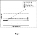
- the systems and methods described herein can be used in a system to tolerate higher input voltages without experiencing runaway currents (for example as illustrated in Fig. 3 ).
- a circuit 100 can comprise an optical coupling 102, including an illuminator 104 optically coupled to an optical sensor 106.
- the optical coupling 102 can be configured to output a voltage from the optical sensor 106 based on intensity of illumination from the illuminator 104.
- the circuit 100 can include a voltage input node 108, a Zener diode 134, and a resistance 110, where the resistance 110 can be connected in series between the voltage input node 108 and the Zener diode 134.
- the resistance 110 can include two resistors (e.g. 130, 132) connected in series with one another, for example as shown in Fig. 1 , however, any suitable number of resistors can be used.
- the Zener diode 134 can be oriented in the circuit 100 to block current from the voltage input node 108 through the resistance 110 below a threshold voltage and oriented to allow current from the voltage input node 108 through the resistance 110 above the threshold voltage.
- the Zener diode 134 can be operatively connected to the illuminator 104 to power the illuminator 104 with voltage from the voltage input node 108.
- the circuit 100 can further include a current limiter 114 connected between the voltage input node 108 and the Zener diode 134 to provide consistent current to the illuminator 104 above the threshold voltage.
- Zener diodes 112,136 can form the same Zener diode, for example, the circuit can include only two Zener diodes 112/136 and 134. By splitting the diodes 112,136, it is possible to reduce the max power of each diode and/or to select differing thresholds. Therefore, Zener diodes 112,136 will be hereafter referred to as a single component 112/136.
- the current limiter 114 can include a switching component 116.
- the switching component can include a drain 118 connected to the voltage input node 108, and a source 120 connected to a first node 122 in series between the Zener diode 112/136 and the resistance 110.
- the switching component can also include a gate 124 connected to a second node 126 in series between the resistance 110 and the first node 122.
- the switching component 116 can be a MOSFET, e.g. as shown in Fig. 1 , however any suitable switching component can be included.
- the source 120 of the switching component 116 can connect to the first node 122 through a source resistor 128.
- the Zener diode 112/136 can be a first Zener diode 112/136 and the circuit 100 can include a second Zener diode 134 in series between the first and second nodes 122 and 126. It is contemplated that the second Zener diode 134 can be oriented in the same direction with respect to the voltage input node 108 as is the first Zener diode 112/136. Further, the circuit 100 can include a non-Zener diode 138 in series between the Zener diode 112 and the illuminator 104, wherein the diode 138 is oriented opposite the orientation of the Zener diode 112/136.
- the voltage input node 108 can be a first voltage input node 140 configured to provide voltage from a first phase of an electrical heated oven 150.
- the circuit 100 can also include a second input node 142 configured to provide voltage from a second phase of the electrical heated oven 152.
- ovens 150 and 152 are shown schematically in Fig. 1 connected to voltage input nodes 140 and 142 respectively.
- the illuminator 104 can be a light emitting diode (LED)(e.g. as shown schematically in Fig. 1 ), however, any suitable illuminator can be used.
- the LED 104 can be connected in series between the first voltage input node 108 and the second voltage input node 142.
- the LED 104 can be oriented to allow current flow from the first voltage input node 108 to the second voltage input node 142.
- the circuit 100 can include a parallel diode 144 connected to the first and second voltage input nodes 140, 142 in parallel with the LED 104 but with opposite orientation.
- a method 200 includes, at box 202, limiting current between a voltage input node 108 and an illuminator 104.
- the method 200 can include powering the illuminator 104 with current from a first voltage input node 108,140,142.
- the method 200 can include sensing illumination level in illumination from the illuminator 104 with a sensor (e.g. optical sensor 106), as shown at box 206.
- the method 200 can include, as shown in box 208, outputting output proportionate to illumination sensed by the sensor 106 indicative of voltage detected at the voltage input node 108,140,142.
- powering the illuminator 104 e.g. box 202 and outputting (e.g. box 204) can be performed while maintaining galvanic insulation between the illuminator 104 and the sensor 106.
- a light emitting diode connected between the voltage input node 108 connected to a first phase heating element (e.g. oven 150) and a second voltage input node 142 connected to a second phase heating element (e.g. oven 152).
- a circuit as shown in Fig. 1 can tolerate higher input voltages without experiencing runaway currents than in traditional techniques.
- conventional circuits (conventional circuit not shown) included a neutral line for 3-phase power, without a current limiter.
- the current increases rapidly when the supply voltage increases (e.g. due to the removal of the neutral line).
- the circuit can be highly influenced by the large tolerance and non-linearity of the optocoupler current transfer ratio.
- power will increase exponentially with input voltage thus resulting in large power consumption in the series resistors and Zener diode.
- the circuit as shown in Fig. 1 having a current limiter therefore allows for better precision in voltage detection and assures a consistent current through the circuit at any voltage above the threshold.
- Fig. 3 shows graphically the current running through the circuit at any point in voltage.
- the upper threshold can be the current required to be certain that the voltage output provided by the circuit in Fig. 1 (e.g. optical sensor 106) is detectable, while taking into account the worst case situation (e.g. production tolerances (lowest LED efficiency, lowest sensitivity optical sensor), worst case temperature, and degradation due to aging.
- the lower threshold refers to a system where each component is in optimal condition (e.g., highest LED efficiency, highest sensitivity optical sensor), best case temperature, and no degradation due to aging.
- the threshold can be considered the tolerance due to the optical coupler.
Landscapes
- Engineering & Computer Science (AREA)
- Physics & Mathematics (AREA)
- General Physics & Mathematics (AREA)
- Electromagnetism (AREA)
- Radar, Positioning & Navigation (AREA)
- Automation & Control Theory (AREA)
- Computer Hardware Design (AREA)
- Microelectronics & Electronic Packaging (AREA)
- Measurement Of Current Or Voltage (AREA)
- Circuit Arrangement For Electric Light Sources In General (AREA)
Abstract
Description
- The present disclosure relates to voltage detection, and more particularly to voltage detection such as used in ovens aboard aircraft.
- A voltage detection circuit is used to determine if an input voltage is above a certain level where the device (e.g. aircraft galley oven) will function properly. Traditional voltage detection circuits for this application have been built around an optical coupler to provide galvanic insulation. Generally, these circuits contain a Zener diode that defines a minimum voltage threshold to which the circuit has to respond. Once the threshold is reached resistors are intended to limit the current. A non-Zener diode is used to block reverse currents, resulting in the circuit only responding to half the sine wave. But in conventional circuits power can increase exponentially with input voltage resulting in runaway currents.
- The conventional techniques have been considered satisfactory for their intended purpose. However, there is an ever present need for improved systems and methods for isolated voltage detection with improved voltage tolerance. This disclosure provides a solution for this need.
- A circuit comprises an optical coupling including an illuminator optically coupled to an optical sensor to output a voltage from the optical sensor based on intensity of illumination from the illuminator. The circuit includes a voltage input node with a resistance connected in series between the voltage input and a Zener diode. The Zener diode is oriented to block current from the voltage input node through the resistance below a threshold voltage, and to allow current from the voltage input node through the resistance above the threshold voltage. The Zener diode is operatively connected to the illuminator to power the illuminator. The circuit further comprises a current limiter connected between the voltage input node and the Zener diode to provide consistent current to the illuminator above the threshold voltage.
- The current limiter can include a switching component with a drain connected to the voltage input node. The current limiter can include a source connected to a first node in series between the Zener diode and the resistance and a gate connected to a second node in series between the resistance and the first node. The switching device can be a MOSFET. The source of the switching device can connect to the first node through a source resistor. The resistance can include two resistors connected in series with one another.
- The Zener diode can be a first Zener diode and the circuit can include a second Zener diode in series between the first and second node. The second Zener diode can be oriented in the same direction with respect to the voltage input node as is the first Zener diode. The circuit can include a third Zener diode in series between the second first node and the first Zener diode. The third Zener diode can be oriented in the same direction with respect to the voltage input node as are the first and second Zener diodes. The circuit can include a diode in series between the Zener diode and the illuminator, wherein the diode is oriented opposite the orientation of the Zener diode.
- The voltage input node can be a first voltage input node configured to provide voltage from a first phase of an electrical heated oven. The voltage input node can include a second input node configured to provide voltage from a second phase of the electrical heated oven.
- The illuminator can be a light emitting diode (LED) connected in series between the first voltage input node and the second voltage input node. The LED can be oriented to allow current flow from the first voltage input node to the second voltage input node. The circuit can include a parallel diode connected to the first and second voltage input nodes in parallel with the LED but with opposite orientation.
- A method includes powering an illuminator with current from a first voltage input node. The method includes sensing illumination level in illumination from the illuminator with a sensor and outputting output proportionate to illumination sensed by the sensor indicative of voltage detected at the voltage input node. The method can include limiting current between the voltage input node and the illuminator.
- In the method, powering the illuminator and outputting can be performed while maintaining galvanic insulation between the illuminator and the sensor. Limiting current can include using a switching component with a drain connected to the voltage input node, a source connected to a first node in series between a Zener diode and a resistance, and a gate connected to a second node in series between the resistance and the first node. The illuminator can include powering a light emitting diode (LED) connected between the voltage input node connected to a first phase heating element and a second voltage input node connected to a second phase heating element.
- These and other features of the systems and methods of the subject disclosure will become more readily apparent to those skilled in the art from the following detailed description of the embodiments taken in conjunction with the drawings.
- So that those skilled in the art to which the subject disclosure appertains will readily understand how to make and use the devices and methods of the subject disclosure without undue experimentation, embodiments thereof will be described in detail herein below with reference to certain figures, wherein:
-
Fig. 1 is a schematic circuit diagram of an embodiment of a circuit in accordance with the present disclosure, showing an isolated voltage detection circuit; -
Fig. 2 is a schematic diagram of a method for detecting voltage in a circuit; and -
Fig. 3 is a graphical view showing the current limiting effects of the system ofFig. 1 . - Reference will now be made to the drawings wherein like reference numerals identify similar structural features or aspects of the subject disclosure. For purposes of explanation and illustration, and not limitation, a schematic diagram of an embodiment of a circuit in accordance with the disclosure is shown in
Fig. 1 and is designated generally byreference character 100. Other embodiments of systems in accordance with the disclosure, or aspects thereof, are provided inFigs. 2-3 , as will be described. The systems and methods described herein can be used in a system to tolerate higher input voltages without experiencing runaway currents (for example as illustrated inFig. 3 ). - Referring to
Fig. 1 , acircuit 100 can comprise anoptical coupling 102, including anilluminator 104 optically coupled to anoptical sensor 106. Theoptical coupling 102 can be configured to output a voltage from theoptical sensor 106 based on intensity of illumination from theilluminator 104. Thecircuit 100 can include a voltage input node 108, a Zenerdiode 134, and aresistance 110, where theresistance 110 can be connected in series between the voltage input node 108 and the Zenerdiode 134. It is contemplated that theresistance 110 can include two resistors (e.g. 130, 132) connected in series with one another, for example as shown inFig. 1 , however, any suitable number of resistors can be used. - In embodiments, the Zener
diode 134 can be oriented in thecircuit 100 to block current from the voltage input node 108 through theresistance 110 below a threshold voltage and oriented to allow current from the voltage input node 108 through theresistance 110 above the threshold voltage. The Zenerdiode 134 can be operatively connected to theilluminator 104 to power theilluminator 104 with voltage from the voltage input node 108. In embodiments, thecircuit 100 can further include acurrent limiter 114 connected between the voltage input node 108 and the Zenerdiode 134 to provide consistent current to theilluminator 104 above the threshold voltage. While the circuit shows multiple Zenerdiodes diodes 112/136 and 134. By splitting the diodes 112,136, it is possible to reduce the max power of each diode and/or to select differing thresholds. Therefore, Zener diodes 112,136 will be hereafter referred to as asingle component 112/136. - The
current limiter 114 can include aswitching component 116. The switching component can include a drain 118 connected to the voltage input node 108, and a source 120 connected to afirst node 122 in series between the Zenerdiode 112/136 and theresistance 110. The switching component can also include agate 124 connected to asecond node 126 in series between theresistance 110 and thefirst node 122. In embodiments, theswitching component 116 can be a MOSFET, e.g. as shown inFig. 1 , however any suitable switching component can be included. The source 120 of theswitching component 116 can connect to thefirst node 122 through asource resistor 128. - In embodiments, the
Zener diode 112/136 can be afirst Zener diode 112/136 and thecircuit 100 can include asecond Zener diode 134 in series between the first andsecond nodes second Zener diode 134 can be oriented in the same direction with respect to the voltage input node 108 as is thefirst Zener diode 112/136. Further, thecircuit 100 can include anon-Zener diode 138 in series between theZener diode 112 and theilluminator 104, wherein thediode 138 is oriented opposite the orientation of theZener diode 112/136. - As shown in
Fig. 1 , the voltage input node 108 can be a first voltage input node 140 configured to provide voltage from a first phase of an electricalheated oven 150. In embodiments, thecircuit 100 can also include asecond input node 142 configured to provide voltage from a second phase of the electricalheated oven 152. For the sake of clarity,ovens Fig. 1 connected tovoltage input nodes 140 and 142 respectively. - In embodiments, the
illuminator 104 can be a light emitting diode (LED)(e.g. as shown schematically inFig. 1 ), however, any suitable illuminator can be used. TheLED 104 can be connected in series between the first voltage input node 108 and the secondvoltage input node 142. TheLED 104 can be oriented to allow current flow from the first voltage input node 108 to the secondvoltage input node 142. In further embodiments, thecircuit 100 can include aparallel diode 144 connected to the first and secondvoltage input nodes 140, 142 in parallel with theLED 104 but with opposite orientation. - Referring now to
Fig. 2 , amethod 200 includes, atbox 202, limiting current between a voltage input node 108 and anilluminator 104. Atbox 204, themethod 200 can include powering theilluminator 104 with current from a first voltage input node 108,140,142. Themethod 200 can include sensing illumination level in illumination from theilluminator 104 with a sensor (e.g. optical sensor 106), as shown atbox 206. In embodiments, themethod 200 can include, as shown inbox 208, outputting output proportionate to illumination sensed by thesensor 106 indicative of voltage detected at the voltage input node 108,140,142. - In the
method 200, powering the illuminator 104 (e.g. box 202) and outputting (e.g. box 204) can be performed while maintaining galvanic insulation between the illuminator 104 and thesensor 106. Limiting current (e.g. box 208) can include using aswitching component 116 with a drain 118 connected to the voltage input node 108, a source 120 connected to afirst node 122 in series between aZener diode 112/136 and aresistance 110, and agate 124 connected to asecond node 126 in series between theresistance 110 and thefirst node 122. Powering the illuminator 104 (e.g. as in box 202) can include powering a light emitting diode (LED) connected between the voltage input node 108 connected to a first phase heating element (e.g. oven 150) and a secondvoltage input node 142 connected to a second phase heating element (e.g. oven 152). - Turning to
Fig. 3 , a circuit as shown inFig. 1 can tolerate higher input voltages without experiencing runaway currents than in traditional techniques. For example, conventional circuits (conventional circuit not shown) included a neutral line for 3-phase power, without a current limiter. In that case, the current increases rapidly when the supply voltage increases (e.g. due to the removal of the neutral line). As a result the circuit can be highly influenced by the large tolerance and non-linearity of the optocoupler current transfer ratio. Further, without a current limiter as in the conventional circuit, power will increase exponentially with input voltage thus resulting in large power consumption in the series resistors and Zener diode. The circuit as shown inFig. 1 having a current limiter therefore allows for better precision in voltage detection and assures a consistent current through the circuit at any voltage above the threshold. - More particularly,
Fig. 3 shows graphically the current running through the circuit at any point in voltage. The upper threshold can be the current required to be certain that the voltage output provided by the circuit inFig. 1 (e.g. optical sensor 106) is detectable, while taking into account the worst case situation (e.g. production tolerances (lowest LED efficiency, lowest sensitivity optical sensor), worst case temperature, and degradation due to aging. The lower threshold refers to a system where each component is in optimal condition (e.g., highest LED efficiency, highest sensitivity optical sensor), best case temperature, and no degradation due to aging. The threshold can be considered the tolerance due to the optical coupler. - The methods and systems of the present disclosure, as described above and shown in the drawings, provide for increased precision in voltage detection and increased voltage tolerance. While the apparatus and methods of the subject disclosure have been shown and described with reference to embodiments, those skilled in the art will readily appreciate that changes and/or modifications may be made thereto without departing from the scope of the invention as defined by the claims.
Claims (15)
- A circuit comprising:an optical coupling (102) including an illuminator (104) optically coupled to an optical sensor (106) to output a voltage from the optical sensor based on intensity of illumination from the illuminator;a voltage input node (108) with a resistance (110) connected in series between the voltage input and a Zener diode (112, 136) oriented to block current from the voltage input node through the resistance below a threshold voltage, and to allow current from the voltage input node through the resistance above the threshold voltage, wherein the Zener diode is operatively connected to the illuminator to power the illuminator; anda current limiter (114) connected between the voltage input node and the Zener diode to provide consistent current to the illuminator above the threshold voltage.
- The circuit as recited in claim 1, wherein the current limiter includes a switching component (116) with a drain (118) connected to the voltage input node, a source (120) connected to a first node (122) in series between the Zener diode and the resistance, and a gate (124) connected to a second node (126) in series between the resistance and the first node.
- The circuit as recited in claim 2, wherein the switching component is a MOSFET.
- The circuit as recited in claim 2 or 3, wherein the source of the switching component connects to the first node through a source resistor (128).
- The circuit as recited in any of claims 2 to 4, wherein the Zener diode is a first Zener diode (112, 136) and further comprising a second Zener diode (134) in series between the first (122) and second (126) nodes, wherein the second Zener diode is oriented in the same direction with respect to the voltage input node as is the first Zener diode.
- The circuit as recited in claim 5, further comprising a third Zener diode (136) in series between the second node and the first Zener diode, wherein the third Zener diode is oriented in the same direction with respect to the voltage input node as are the first and second Zener diodes.
- The circuit as recited in any preceding claim, further comprising a diode (138) in series between the Zener diode and the illuminator, wherein the diode is oriented opposite the orientation of the Zener diode.
- The circuit as recited in any preceding claim, wherein the voltage input node is a first voltage input node configured to provide voltage from a first phase of an electrical heated oven, and further comprising a second input node (142) configured to provide voltage from a second phase of the electrical heated oven.
- The circuit as recited in claim 8, wherein the illuminator is a light emitting diode LED connected in series between the first voltage input node and the second voltage input node, wherein the LED is oriented to allow current flow from the first voltage input node to the second voltage input node.
- The circuit as recited in claim 9, further comprising a parallel diode (144) connected to the first and second voltage input nodes in parallel with the LED but with opposite orientation.
- The circuit as recited in any preceding claim, wherein in the resistance includes two resistors (130, 132) connected in series with one another.
- A method of voltage detection in an aircraft oven comprising:powering an illuminator (104) with current from a first voltage input node (108);sensing illumination level in illumination from the illuminator with a sensor (106) and outputting output proportionate to illumination sensed by the sensor indicative of voltage detected at the voltage input node, wherein powering the illuminator includes limiting current between the voltage input node and the illuminator.
- The method as recited in claim 12, wherein powering the illuminator and outputting are performed while maintaining galvanic insulation between the illuminator and the sensor.
- The method as recited in claim 12 or 13, wherein limiting current includes using a switching component (116) with a drain (118) connected to the voltage input node, a source (120) connected to a first node (122) in series between a Zener diode (112) and a resistance (110), and a gate (124) connected to a second node (126) in series between the resistance and the first node.
- The method as recited in claim 12, 13 or 14, wherein powering the illuminator includes powering a light emitting diode LED connected between the voltage input node connected to a first phase heating element and a second voltage input node connected to a second phase heating element.
Applications Claiming Priority (1)
| Application Number | Priority Date | Filing Date | Title |
|---|---|---|---|
| US17/132,961 US11602022B2 (en) | 2020-12-23 | 2020-12-23 | Isolated voltage detection with current limiters |
Publications (1)
| Publication Number | Publication Date |
|---|---|
| EP4020807A1 true EP4020807A1 (en) | 2022-06-29 |
Family
ID=79021100
Family Applications (1)
| Application Number | Title | Priority Date | Filing Date |
|---|---|---|---|
| EP21217063.3A Withdrawn EP4020807A1 (en) | 2020-12-23 | 2021-12-22 | Isolated voltage detection with current limiters |
Country Status (2)
| Country | Link |
|---|---|
| US (1) | US11602022B2 (en) |
| EP (1) | EP4020807A1 (en) |
Cited By (1)
| Publication number | Priority date | Publication date | Assignee | Title |
|---|---|---|---|---|
| WO2024023828A1 (en) * | 2022-07-27 | 2024-02-01 | Pwr Nukleus Technologies Private Limited | A voltage tester device/system for safety application in electrical panel and method thereof |
Citations (4)
| Publication number | Priority date | Publication date | Assignee | Title |
|---|---|---|---|---|
| GB2030765A (en) * | 1978-10-02 | 1980-04-10 | Lumenition Ltd | Darlington transistor pairs |
| US20130334201A1 (en) * | 2012-06-19 | 2013-12-19 | Larry Nicholson | Portable Spa Monitoring And Control Circuitry |
| US20160336938A1 (en) * | 2014-02-04 | 2016-11-17 | Phoenix Contact Gmbh & Co. Kg | Large-range input circuit |
| DE102016203419A1 (en) * | 2016-03-02 | 2017-09-07 | Siemens Aktiengesellschaft | Cascadable circuit for a signal injection system |
Family Cites Families (19)
| Publication number | Priority date | Publication date | Assignee | Title |
|---|---|---|---|---|
| DE10048189A1 (en) * | 2000-09-28 | 2002-04-11 | Patent Treuhand Ges Fuer Elektrische Gluehlampen Mbh | Circuit arrangement for regulating an analog voltage signal |
| EP1387460B1 (en) | 2002-08-02 | 2007-09-12 | Airbus Deutschland GmbH | Power supply arrangement for the galley of a vehicle, in particular for an aircraft |
| US7721564B2 (en) | 2006-11-21 | 2010-05-25 | B/E Aerospace, Inc. | Wild frequency avionic refrigeration system and controller therefor |
| US8289670B2 (en) | 2007-10-17 | 2012-10-16 | B/E Intellectual Property | Adaptive power management system for aircraft galleys |
| US8102080B2 (en) * | 2007-12-28 | 2012-01-24 | General Electric Company | Control system for an appliance |
| DE102010043613A1 (en) * | 2010-11-09 | 2012-05-10 | Tridonic Gmbh & Co. Kg | Interference-proof lighting control |
| US8841860B2 (en) * | 2011-12-15 | 2014-09-23 | Cree, Inc. | SIMO converters that generate a light output |
| CN102752912B (en) * | 2012-06-01 | 2015-11-25 | 台达电子企业管理(上海)有限公司 | A kind of LED drive circuit |
| US9112345B2 (en) | 2012-06-06 | 2015-08-18 | Honeywell International Inc. | In-rush current limiter and method for stowable and carry-on devices |
| WO2014013454A2 (en) * | 2012-07-20 | 2014-01-23 | Koninklijke Philips N.V. | Digital communication interface circuit for line-pair with duty cycle imbalance compensation |
| EP2961654A4 (en) | 2013-02-28 | 2016-11-16 | Bae Sys Controls Inc | SYSTEMS AND METHODS FOR FEEDING SEATS |
| CN104600707A (en) | 2015-01-12 | 2015-05-06 | 国家电网公司 | Current limiting type UPFC system design method |
| US10270240B2 (en) * | 2015-10-08 | 2019-04-23 | Hubbell Incorporated | Surge protective device with abnormal overvoltage protection |
| US10384802B2 (en) | 2016-02-19 | 2019-08-20 | The Boeing Company | Real time galley power management and fault monitoring system |
| CN106787655A (en) | 2016-12-29 | 2017-05-31 | 国网浙江省电力公司绍兴供电公司 | A kind of current-limiting type UPFC DC side overvoltage protection circuits |
| CN206481047U (en) | 2016-12-29 | 2017-09-08 | 国网浙江省电力公司绍兴供电公司 | A kind of current-limiting type UPFC protects system |
| CN106787656A (en) | 2016-12-29 | 2017-05-31 | 国网浙江省电力公司绍兴供电公司 | A kind of current-limiting type UPFC DC side overvoltage protective systems |
| FR3085153B1 (en) | 2018-08-21 | 2020-08-28 | Safran Electrical & Power | PROCESS FOR PROTECTING A LOAD ASSOCIATED WITH A CIRCUIT BREAKER CHANNEL OF AN ELECTRONIC BOARD OF STATIC CIRCUIT BREAKERS |
| US10750601B1 (en) * | 2019-10-01 | 2020-08-18 | Abl Ip Holding Llc | Lighting fixture commissioning based on powerline signaling techniques |
-
2020
- 2020-12-23 US US17/132,961 patent/US11602022B2/en active Active
-
2021
- 2021-12-22 EP EP21217063.3A patent/EP4020807A1/en not_active Withdrawn
Patent Citations (4)
| Publication number | Priority date | Publication date | Assignee | Title |
|---|---|---|---|---|
| GB2030765A (en) * | 1978-10-02 | 1980-04-10 | Lumenition Ltd | Darlington transistor pairs |
| US20130334201A1 (en) * | 2012-06-19 | 2013-12-19 | Larry Nicholson | Portable Spa Monitoring And Control Circuitry |
| US20160336938A1 (en) * | 2014-02-04 | 2016-11-17 | Phoenix Contact Gmbh & Co. Kg | Large-range input circuit |
| DE102016203419A1 (en) * | 2016-03-02 | 2017-09-07 | Siemens Aktiengesellschaft | Cascadable circuit for a signal injection system |
Cited By (1)
| Publication number | Priority date | Publication date | Assignee | Title |
|---|---|---|---|---|
| WO2024023828A1 (en) * | 2022-07-27 | 2024-02-01 | Pwr Nukleus Technologies Private Limited | A voltage tester device/system for safety application in electrical panel and method thereof |
Also Published As
| Publication number | Publication date |
|---|---|
| US20220201815A1 (en) | 2022-06-23 |
| US11602022B2 (en) | 2023-03-07 |
Similar Documents
| Publication | Publication Date | Title |
|---|---|---|
| US10884036B2 (en) | Alternating current load detection circuit | |
| US9554440B2 (en) | Dimmable LED lighting apparatus | |
| US20150355289A1 (en) | Electronic device | |
| US10257908B2 (en) | LED device protection circuit and method thereof | |
| US11602022B2 (en) | Isolated voltage detection with current limiters | |
| JP5812292B2 (en) | Beacon lights and beacon systems | |
| US8896319B2 (en) | Light emitting device control circuit and short detection circuit thereof | |
| US20170135184A1 (en) | Circuit Assembly For Operating Lighting Means Via A Master-Slave System | |
| US11408921B2 (en) | Circuit and method for realizing a combined connection of neutral wires or live wires using phase information of the neutral wires and the live wires | |
| CN112449466B (en) | Linear LED driving circuit, power switch detection method and dimming control method | |
| US20150043660A1 (en) | Closed-circuit power line communication system for large capacity load | |
| SE437893B (en) | DEVICE FOR DETECTION OF NON-REQUIRED SIGNAL COMBINATIONS FOR TWO SIGNAL LIGHTS IN TRAFFIC LIGHT | |
| US20150022120A1 (en) | Light emitting diode apparatus with over current protection function and system having the same | |
| SE443899B (en) | HIGH VOLTAGE CONVERTERS, INCLUDING A MULTIPLE SERIES-CONNECTED THRISTORS | |
| JPH11110049A (en) | Water level controller | |
| US9641171B2 (en) | Large-range input circuit | |
| US6169491B1 (en) | Multiport power monitor | |
| CN216595395U (en) | Open circuit detection circuit of LED parallel circuit and electronic equipment | |
| JP7011446B2 (en) | Short-circuit judgment device and light irradiation device | |
| JPS5932319A (en) | Thyristor switch defect monitor system | |
| US20150253361A1 (en) | Voltage Monitoring Circuit | |
| US5925888A (en) | Optocoupler input expansion circuit | |
| CN111405722A (en) | Light modulator | |
| JP2016021305A (en) | Remote control device for led lighting power source | |
| KR101340295B1 (en) | LED Lighting System for decreasing the variation in current to that in temperature |
Legal Events
| Date | Code | Title | Description |
|---|---|---|---|
| PUAI | Public reference made under article 153(3) epc to a published international application that has entered the european phase |
Free format text: ORIGINAL CODE: 0009012 |
|
| STAA | Information on the status of an ep patent application or granted ep patent |
Free format text: STATUS: THE APPLICATION HAS BEEN PUBLISHED |
|
| AK | Designated contracting states |
Kind code of ref document: A1 Designated state(s): AL AT BE BG CH CY CZ DE DK EE ES FI FR GB GR HR HU IE IS IT LI LT LU LV MC MK MT NL NO PL PT RO RS SE SI SK SM TR |
|
| STAA | Information on the status of an ep patent application or granted ep patent |
Free format text: STATUS: REQUEST FOR EXAMINATION WAS MADE |
|
| 17P | Request for examination filed |
Effective date: 20221228 |
|
| RBV | Designated contracting states (corrected) |
Designated state(s): AL AT BE BG CH CY CZ DE DK EE ES FI FR GB GR HR HU IE IS IT LI LT LU LV MC MK MT NL NO PL PT RO RS SE SI SK SM TR |
|
| STAA | Information on the status of an ep patent application or granted ep patent |
Free format text: STATUS: EXAMINATION IS IN PROGRESS |
|
| 17Q | First examination report despatched |
Effective date: 20240129 |
|
| RAP1 | Party data changed (applicant data changed or rights of an application transferred) |
Owner name: B/E AEROSPACE INC. |
|
| STAA | Information on the status of an ep patent application or granted ep patent |
Free format text: STATUS: THE APPLICATION HAS BEEN WITHDRAWN |
|
| 18W | Application withdrawn |
Effective date: 20260306 |