EP4020603A1 - Method for forming a photovoltaic device with group v dopants - Google Patents
Method for forming a photovoltaic device with group v dopants Download PDFInfo
- Publication number
- EP4020603A1 EP4020603A1 EP22155897.6A EP22155897A EP4020603A1 EP 4020603 A1 EP4020603 A1 EP 4020603A1 EP 22155897 A EP22155897 A EP 22155897A EP 4020603 A1 EP4020603 A1 EP 4020603A1
- Authority
- EP
- European Patent Office
- Prior art keywords
- absorber layer
- layer
- alkali metal
- photovoltaic device
- group
- Prior art date
- Legal status (The legal status is an assumption and is not a legal conclusion. Google has not performed a legal analysis and makes no representation as to the accuracy of the status listed.)
- Pending
Links
Images


Classifications
-
- H—ELECTRICITY
- H10—SEMICONDUCTOR DEVICES; ELECTRIC SOLID-STATE DEVICES NOT OTHERWISE PROVIDED FOR
- H10F—INORGANIC SEMICONDUCTOR DEVICES SENSITIVE TO INFRARED RADIATION, LIGHT, ELECTROMAGNETIC RADIATION OF SHORTER WAVELENGTH OR CORPUSCULAR RADIATION
- H10F77/00—Constructional details of devices covered by this subclass
- H10F77/10—Semiconductor bodies
- H10F77/12—Active materials
- H10F77/123—Active materials comprising only Group II-VI materials, e.g. CdS, ZnS or HgCdTe
- H10F77/1233—Active materials comprising only Group II-VI materials, e.g. CdS, ZnS or HgCdTe characterised by the dopants
-
- H—ELECTRICITY
- H10—SEMICONDUCTOR DEVICES; ELECTRIC SOLID-STATE DEVICES NOT OTHERWISE PROVIDED FOR
- H10F—INORGANIC SEMICONDUCTOR DEVICES SENSITIVE TO INFRARED RADIATION, LIGHT, ELECTROMAGNETIC RADIATION OF SHORTER WAVELENGTH OR CORPUSCULAR RADIATION
- H10F10/00—Individual photovoltaic cells, e.g. solar cells
- H10F10/10—Individual photovoltaic cells, e.g. solar cells having potential barriers
- H10F10/16—Photovoltaic cells having only PN heterojunction potential barriers
- H10F10/162—Photovoltaic cells having only PN heterojunction potential barriers comprising only Group II-VI materials, e.g. CdS/CdTe photovoltaic cells
-
- H—ELECTRICITY
- H10—SEMICONDUCTOR DEVICES; ELECTRIC SOLID-STATE DEVICES NOT OTHERWISE PROVIDED FOR
- H10F—INORGANIC SEMICONDUCTOR DEVICES SENSITIVE TO INFRARED RADIATION, LIGHT, ELECTROMAGNETIC RADIATION OF SHORTER WAVELENGTH OR CORPUSCULAR RADIATION
- H10F19/00—Integrated devices, or assemblies of multiple devices, comprising at least one photovoltaic cell covered by group H10F10/00, e.g. photovoltaic modules
- H10F19/80—Encapsulations or containers for integrated devices, or assemblies of multiple devices, having photovoltaic cells
- H10F19/807—Double-glass encapsulation, e.g. photovoltaic cells arranged between front and rear glass sheets
-
- H—ELECTRICITY
- H10—SEMICONDUCTOR DEVICES; ELECTRIC SOLID-STATE DEVICES NOT OTHERWISE PROVIDED FOR
- H10F—INORGANIC SEMICONDUCTOR DEVICES SENSITIVE TO INFRARED RADIATION, LIGHT, ELECTROMAGNETIC RADIATION OF SHORTER WAVELENGTH OR CORPUSCULAR RADIATION
- H10F71/00—Manufacture or treatment of devices covered by this subclass
- H10F71/125—The active layers comprising only Group II-VI materials, e.g. CdS, ZnS or CdTe
- H10F71/1253—The active layers comprising only Group II-VI materials, e.g. CdS, ZnS or CdTe comprising at least three elements, e.g. HgCdTe
-
- H—ELECTRICITY
- H10—SEMICONDUCTOR DEVICES; ELECTRIC SOLID-STATE DEVICES NOT OTHERWISE PROVIDED FOR
- H10F—INORGANIC SEMICONDUCTOR DEVICES SENSITIVE TO INFRARED RADIATION, LIGHT, ELECTROMAGNETIC RADIATION OF SHORTER WAVELENGTH OR CORPUSCULAR RADIATION
- H10F71/00—Manufacture or treatment of devices covered by this subclass
- H10F71/128—Annealing
-
- H—ELECTRICITY
- H10—SEMICONDUCTOR DEVICES; ELECTRIC SOLID-STATE DEVICES NOT OTHERWISE PROVIDED FOR
- H10F—INORGANIC SEMICONDUCTOR DEVICES SENSITIVE TO INFRARED RADIATION, LIGHT, ELECTROMAGNETIC RADIATION OF SHORTER WAVELENGTH OR CORPUSCULAR RADIATION
- H10F71/00—Manufacture or treatment of devices covered by this subclass
- H10F71/131—Recrystallisation; Crystallization of amorphous or microcrystalline semiconductors
-
- H—ELECTRICITY
- H10—SEMICONDUCTOR DEVICES; ELECTRIC SOLID-STATE DEVICES NOT OTHERWISE PROVIDED FOR
- H10F—INORGANIC SEMICONDUCTOR DEVICES SENSITIVE TO INFRARED RADIATION, LIGHT, ELECTROMAGNETIC RADIATION OF SHORTER WAVELENGTH OR CORPUSCULAR RADIATION
- H10F77/00—Constructional details of devices covered by this subclass
- H10F77/10—Semiconductor bodies
- H10F77/12—Active materials
- H10F77/123—Active materials comprising only Group II-VI materials, e.g. CdS, ZnS or HgCdTe
- H10F77/1237—Active materials comprising only Group II-VI materials, e.g. CdS, ZnS or HgCdTe having at least three elements, e.g. HgCdTe
-
- Y—GENERAL TAGGING OF NEW TECHNOLOGICAL DEVELOPMENTS; GENERAL TAGGING OF CROSS-SECTIONAL TECHNOLOGIES SPANNING OVER SEVERAL SECTIONS OF THE IPC; TECHNICAL SUBJECTS COVERED BY FORMER USPC CROSS-REFERENCE ART COLLECTIONS [XRACs] AND DIGESTS
- Y02—TECHNOLOGIES OR APPLICATIONS FOR MITIGATION OR ADAPTATION AGAINST CLIMATE CHANGE
- Y02E—REDUCTION OF GREENHOUSE GAS [GHG] EMISSIONS, RELATED TO ENERGY GENERATION, TRANSMISSION OR DISTRIBUTION
- Y02E10/00—Energy generation through renewable energy sources
- Y02E10/50—Photovoltaic [PV] energy
- Y02E10/543—Solar cells from Group II-VI materials
Definitions
- the present specification generally relates to efficient photovoltaic devices and methods for forming the same and, more specifically, to photovoltaic devices and semiconductor layers with group V having enhanced carrier concentration and methods for forming the same.
- a photovoltaic device generates electrical power by converting light into electricity using semiconductor materials that exhibit the photovoltaic effect.
- the manufacturing processes necessary to efficiently produce the photovoltaic device can exacerbate undesirable properties of the photovoltaic device.
- semiconductor layers are sometimes subjected to chloride heat treatment (CHT), which is an annealing process in a chlorine and oxygen containing atmosphere.
- CHT chloride heat treatment
- the CHT can improve the crystalline quality of the semiconductor layer.
- the grain (crystallite) size can be increased.
- defects in the lattice structure can be cured including, for example, defects located at grain boundary areas. Defects in the lattice structure can be sources of carrier recombination, which reduces photovoltaic efficiency.
- the semiconductor layer can be doped with materials, i.e., dopants, which can be activated to increase the charge carrier concentration of the semiconductor layer.
- dopants i.e., dopants
- the addition of dopants to a semiconductor layer can produce a material layer with predominantly negative, n-type, or positive, p-type, charge carriers.
- subjecting a doped semiconductor layer to the CHT can result in a doped semiconductor layer with an insufficient charge carrier concentration, i.e., the charge carrier concentration can be too low.
- a large of a proportion of the dopant can fail to activate, and fail to contribute to the generation of electrical power.
- Embodiments of a photovoltaic device for generating electrical power from light are described herein.
- the photovoltaic device generally includes an absorber layer formed from a semiconductor material.
- the absorber layer can be subjected to one or more processing steps configured to activate the dopant.
- activate or activation can mean manipulating a dopant such that the dopant operates as a charge carrier within a semiconductor, e.g., activated p-type dopants operate as acceptors.
- activated p-type dopants operate as acceptors.
- the photovoltaic device 100 can be configured to receive light and transform light into electrical signals, e.g., photons can be absorbed from the light and transformed into electrical signals via the photovoltaic effect. Accordingly, the photovoltaic device 100 can define an energy side 102 configured to be exposed to a light source such as, for example, the sun. The photovoltaic device 102 can also define an opposing side 104 offset from the energy side 102. It is noted that the term "light” can refer to various wavelengths of the electromagnetic spectrum such as, but not limited to, wavelengths in the ultraviolet (UV), infrared (IR), and visible portions of the electromagnetic spectrum.
- UV ultraviolet
- IR infrared
- the photovoltaic device 100 can include a plurality of layers disposed between the energy side 102 and the opposing side 104.
- layer refers to a thickness of material provided upon a surface. Each layer can cover all or any portion of the surface.
- the photovoltaic device 100 can include a substrate 110 configured to facilitate the transmission of light into the photovoltaic device 100.
- the substrate 110 can be disposed at the energy side 102 of the photovoltaic device 100. Referring collectively to FIGS. 1 and 2 , the substrate 110 can have a first surface 112 substantially facing the energy side 102 of the photovoltaic device 100 and a second surface 114 substantially facing the opposing side 104 of the photovoltaic device 100.
- One or more layers of material can be disposed between the first surface 112 and the second surface 114 of the substrate 110.
- the substrate 110 can include a transparent layer 120 having a first surface 122 substantially facing the energy side 102 of the photovoltaic device 100 and a second surface 124 substantially facing the opposing side 104 of the photovoltaic device 100.
- the second surface 124 of the transparent layer 120 can form the second surface 114 of the substrate 110.
- the transparent layer 120 can be formed from a substantially transparent material such as, for example, glass. Suitable glass can include soda-lime glass, or any glass with reduced iron content.
- the transparent layer 120 can have any suitable transmittance, including about 450 nm to about 800 nm in some embodiments.
- the transparent layer 120 may also have any suitable transmission percentage, including, for example, more than about 50% in one embodiment, more than about 60% in another embodiment, more than about 70% in yet another embodiment, more than about 80% in a further embodiment, or more than about 85% in still a further embodiment.
- transparent layer 120 can be formed from a glass with about 90% transmittance.
- the substrate 110 can include a coating 126 applied to the first surface 122 of the transparent layer 120.
- the coating 126 can be configured to interact with light or to improve durability of the substrate 110 such as, but not limited to, an antireflective coating, an antisoiling coating, or a combination thereof.
- the photovoltaic device 100 can include a barrier layer 130 configured to mitigate diffusion of contaminants (e.g. sodium) from the substrate 110, which could result in degradation or delamination.
- the barrier layer 130 can have a first surface 132 substantially facing the energy side 102 of the photovoltaic device 100 and a second surface 134 substantially facing the opposing side 104 of the photovoltaic device 100.
- the barrier layer 130 can be provided adjacent to the substrate 110.
- the first surface 132 of the barrier layer 130 can be provided upon the second surface 114 of the substrate 100.
- the phrase "adjacent to," as used herein, means that two layers are disposed contiguously and without any intervening materials between at least a portion of the layers.
- the barrier layer 130 can be substantially transparent, thermally stable, with a reduced number of pin holes and having high sodium-blocking capability, and good adhesive properties. Alternatively or additionally, the barrier layer 130 can be configured to apply color suppression to light.
- the barrier layer 130 can include one or more layers of suitable material, including, but not limited to, tin oxide, silicon dioxide, aluminum-doped silicon oxide, silicon oxide, silicon nitride, or aluminum oxide.
- the barrier layer 130 can have any suitable thickness bounded by the first surface 132 and the second surface 134, including, for example, more than about 500 ⁇ in one embodiment, more than about 750 ⁇ in another embodiment, or less than about 1200 ⁇ in a further embodiment.
- the photovoltaic device 100 can include a transparent conductive oxide (TCO) layer 140 configured to provide electrical contact to transport charge carriers generated by the photovoltaic device 100.
- the TCO layer 140 can have a first surface 142 substantially facing the energy side 102 of the photovoltaic device 100 and a second surface 144 substantially facing the opposing side 104 of the photovoltaic device 100.
- the TCO layer 140 can be provided adjacent to the barrier layer 130.
- the first surface 142 of the TCO layer 140 can be provided upon the second surface 134 of the barrier layer 130.
- the TCO layer 140 can be formed from one or more layers of n-type semiconductor material that is substantially transparent and has a wide band gap.
- the wide band gap can have a larger energy value compared to the energy of the photons of the light, which can mitigate undesired absorption of light.
- the TCO layer 140 can include one or more layers of suitable material, including, but not limited to, tin dioxide, doped tin dioxide (e.g., F-SnO 2 ), indium tin oxide, or cadmium stannate.
- the photovoltaic device 100 can include a buffer layer 150 configured to provide an insulating layer between the TCO layer 140 and any adjacent semiconductor layers.
- the buffer layer 150 can have a first surface 152 substantially facing the energy side 102 of the photovoltaic device 100 and a second surface 154 substantially facing the opposing side 104 of the photovoltaic device 100.
- the buffer layer 150 can be provided adjacent to the TCO layer 140.
- the first surface 152 of the buffer layer 150 can be provided upon the second surface 144 of the TCO layer 140.
- the buffer layer 140 may include material having higher resistivity than the TCO later 140, including, but not limited to, intrinsic tin dioxide, zinc magnesium oxide (e.g., Zn 1-x Mg x O), silicon dioxide (SnO 2 ), aluminum oxide (Al 2 O 3 ), aluminum nitride (AlN), zinc tin oxide, zinc oxide, tin silicon oxide, or any combination thereof.
- the material of the buffer layer 140 can be configured to substantially match the band gap of an adjacent semiconductor layer (e.g., an absorber).
- the buffer layer 150 may have any suitable thickness between the first surface 152 and the second surface 154, including, for example, more than about 100 ⁇ in one embodiment, between about 100 ⁇ and about 800 ⁇ in another embodiment, or between about 150 ⁇ and about 600 ⁇ in a further embodiment.
- the photovoltaic device 100 can include an absorber layer 160 configured to cooperate with another layer and form a p-n junction within the photovoltaic device 100. Accordingly, absorbed photons of the light can free electron-hole pairs and generate carrier flow, which can yield electrical power.
- the absorber layer 160 can have a first surface 162 substantially facing the energy side 102 of the photovoltaic device 100 and a second surface 164 substantially facing the opposing side 104 of the photovoltaic device 100.
- a thickness of the absorber layer 160 can be defined between the first surface 162 and the second surface 164.
- the thickness of the absorber layer 160 can be between about 0.5 ⁇ m to about 10 ⁇ m such as, for example, between about 1 ⁇ m to about 7 ⁇ m in one embodiment, or between about 2 ⁇ m to about 5 ⁇ m in another embodiment.
- the absorber layer 160 can be formed from a p-type semiconductor material having an excess of positive charge carriers, i.e., holes or acceptors.
- the absorber layer 160 can include any suitable p-type semiconductor material such as group II-VI semiconductors. Specific examples include, but are not limited to, semiconductor materials comprising from cadmium, tellurium, selenium, or any combination thereof. Suitable examples include, but are not limited to, cadmium telluride, ternaries of cadmium, selenium and tellurium (e.g., CdSe x Te 1-x ,), or quaternaries comprising cadmium, selenium and tellurium.
- the atomic percent of the selenium can be greater than about 0 atomic percent and less than about 20 atomic percent. In embodiments where the absorber layer 160 comprises tellurium and cadmium, the atomic percent of the tellurium can be greater than about 30 atomic percent and less than about 50 atomic percent. It is noted that the atomic percent described herein is representative of the entirety of the absorber layer 160, the atomic percentage of material at a particular location within the absorber layer 160 can vary with thickness compared to the overall composition of the absorber layer 160. It is noted that the concentration of tellurium, selenium, or both can vary through the thickness of the absorber layer 160.
- x can vary in the absorber layer 160 with distance from the first surface 162 of the absorber layer 160.
- the value of x can decrease in the absorber layer 160 with distance from the first surface 162 of the absorber layer 160.
- the dopant within the absorber layer 160 can be activated to a desired charge carrier concentration.
- the absorber layer 160 can be doped with a group V dopant such as, for example, nitrogen (N), phosphorous (P), arsenic (As), antimony (Sb), bismuth (Bi), ununpentium (Uup), or a combination thereof.
- the total dosage of the dopant within the absorber layer 160 can be controlled.
- an atomic concentration of Group V dopant in a central region 166 the absorber layer 160 can be greater than about 1 ⁇ 10 17 cm -3 such as, for example, between about 1 ⁇ 10 17 cm -3 and about 5 ⁇ 10 20 cm -3 in one embodiment, between about 3 ⁇ 10 17 cm -3 and about 1 ⁇ 10 19 cm -3 in another embodiment, or between about 5 ⁇ 10 17 cm -3 and about 5 ⁇ 10 18 cm -3 in a further embodiment.
- the central region 166 is the middle 50% of the absorber layer 160, which is offset by 25% of the thickness of the absorber layer 160 from each of the first surface 162 and the second surface 164 of the absorber layer 160.
- the concentration profile of the group V dopant can vary through the thickness of the absorber layer 160. Specifically, the amount of the group V dopant can vary with distance from the first surface 162 of the absorber layer 160.
- the p-n junction can be formed by providing the absorber layer 160 sufficiently close to a portion of the photovoltaic device 100 having an excess of negative charge carriers, i.e., electrons or donors.
- the absorber layer 160 can be provided adjacent to n-type semiconductor material.
- one or more intervening layers can be provided between the absorber layer 160 and n-type semiconductor material.
- the absorber layer 160 can be provided adjacent to the buffer layer 150.
- the first surface 162 of the absorber layer 160 can be provided upon the second surface 154 of the buffer layer 150.
- a photovoltaic device 200 can include a window layer 170 comprising n-type semiconductor material. Aside from the window layer 170, the photovoltaic device 200 can have a substantially similar layer structure as the photovoltaic device 100 ( FIG. 1 ).
- the absorber layer 160 can be formed adjacent to the window layer 170.
- the window layer 170 can have a first surface 172 substantially facing the energy side 102 of the photovoltaic device 200 and a second surface 174 substantially facing the opposing side 104 of the photovoltaic device 200.
- the window layer 170 can be positioned between the absorber layer 160 and the TCO layer 140.
- the window layer 170 can be positioned between the absorber layer 160 and the buffer layer 150.
- the window layer 170 can include any suitable material, including, for example, cadmium sulfide, zinc sulfide, cadmium zinc sulfide, zinc magnesium oxide, or any combination thereof.
- the photovoltaic device 100 can include a back contact layer 180 configured to mitigate undesired alteration of the dopant and to provide electrical contact to the absorber layer 160.
- the back contact layer 180 can have a first surface 182 substantially facing the energy side 102 of the photovoltaic device 100 and a second surface 184 substantially facing the opposing side 104 of the photovoltaic device 100.
- a thickness of the back contact layer 180 can be defined between the first surface 182 and the second surface 184.
- the thickness of the back contact layer 180 can be between about 5 nm to about 200 nm such as, for example, between about 10 nm to about 50 nm in one embodiment.
- the back contact layer 180 can be provided adjacent to the absorber layer 160.
- the first surface 182 of the back contact layer 180 can be provided upon the second surface 164 of the absorber layer 160.
- the back contact layer 180 can include binary or ternary combinations of materials from groups I, II, VI, such as for example, one or more layers containing zinc, copper, cadmium and tellurium in various compositions. Further exemplary materials include, but are not limited to, zinc telluride doped with copper telluride, or zinc telluride alloyed with copper telluride.
- the photovoltaic device 100 can include a conducting layer 190 configured to provide electrical contact with the absorber layer 160.
- the conducting layer 190 can have a first surface 192 substantially facing the energy side 102 of the photovoltaic device 100 and a second surface 194 substantially facing the opposing side 104 of the photovoltaic device 100.
- the conducting layer 190 can be provided adjacent to the back contact layer 180.
- the first surface 192 of the conducting layer 190 can be provided upon the second surface 184 of the back contact layer 180.
- the conducting layer 190 can include any suitable conducting material such as, for example, one or more layers of nitrogen-containing metal, silver, nickel, copper, aluminum, titanium, palladium, chrome, molybdenum, gold, or the like.
- Suitable examples of a nitrogen-containing metal layer can include aluminum nitride, nickel nitride, titanium nitride, tungsten nitride, selenium nitride, tantalum nitride, or vanadium nitride.
- the photovoltaic device 100 can include a back support 196 configured to cooperate with the substrate 110 to form a housing for the photovoltaic device 100.
- the back support 196 can be disposed at the opposing side 102 of the photovoltaic device 100.
- the back support 196 can be formed adjacent to conducting layer 190.
- the back support 196 can include any suitable material, including, for example, glass (e.g., soda-lime glass).
- manufacturing of a photovoltaic device 100, 200 generally includes sequentially disposing functional layers or layer precursors in a "stack" of layers through one or more processes, including, but not limited to, sputtering, spray, evaporation, molecular beam deposition, pyrolysis, closed space sublimation (CSS), pulse laser deposition (PLD), chemical vapor deposition (CVD), electrochemical deposition (ECD), atomic layer deposition (ALD), or vapor transport deposition (VTD).
- sputtering spray, evaporation, molecular beam deposition, pyrolysis, closed space sublimation (CSS), pulse laser deposition (PLD), chemical vapor deposition (CVD), electrochemical deposition (ECD), atomic layer deposition (ALD), or vapor transport deposition (VTD).
- a layer of a partially formed device can be processed.
- a partially formed photovoltaic device 202 can comprise the absorber layer 160 adjacent to a layer stack 204.
- the layer stack 204 can include one or more of the layers of the photovoltaic device 100, 200 ( FIGS. 1 and 3 ) disposed between the absorber layer 160 and the energy side 102.
- a partially formed photovoltaic device 206 can comprise the absorber layer 160 adjacent to a layer stack 208.
- the layer stack 208 can include one or more of the layers of the photovoltaic device 100, 200 ( FIGS. 1 and 3 ) between the absorber layer 160 and the opposing side 104.
- the ARHT is an annealing process that employs a chemical compound and a reducing atmosphere.
- the absorber layer 160 can be doped with a group V dopant prior to being subjected to the ARHT.
- the ARHT can be used to activate dopants within the absorber layer 160.
- the ARHT can activate a larger number of dopants and generate a larger carrier concentration than other heat treatment processes, while providing sufficient grain growth within the absorber layer 160.
- the method 200 for performing the ARHT can include a process 212 for exposing the absorber layer 160 to a reducing environment 220.
- the first surface 162 or the second surface 164 of the absorber layer 160 can be subjected to the reducing environment 220.
- the reducing environment 220 is an atmospheric condition in which oxidation is mitigated by removal of oxygen and other oxidizing gases or vapors, i.e., the reducing environment can be substantially free of substances tending to oxidize the Group V dopants.
- the reducing environment 220 can include a forming gas configured to mitigate the formation of group V oxides.
- the forming gas can be energetically more favorable to oxidation than the group V dopant, i.e., an oxidation reaction of the forming gas during the ARHT can have a more negative Gibbs free energy change ( ⁇ G) than the group V dopant.
- the forming gas can comprise hydrogen, nitrogen, or combinations thereof.
- the forming gas consists essentially of a mixture of H 2 and N 2 .
- the forming gas can comprise a mixture of about 50.0 to 99.4% N 2 and about 0.6 to 3.0% H 2 .
- the forming gas can comprise H 2 in an atomic fraction range of 0.5-100%.
- the reducing environment 220 can comprise a forming gas consisting essentially of 100% H 2 .
- suitable reducing agents can include methane (CH 4 ), carbon monoxide (CO), hydrogen sulfide (H 2 S), and ammonia compounds (NH 3 ).
- the reducing environment 220 can be provided within a processing chamber 222 configured to substantially prevent the inclusion of substances tending to oxidize Group V dopants within the reducing environment 220. Accordingly, in some embodiments, the reducing environment 220 can consist essentially of the forming gas. Alternatively or additionally, the processing chamber 222 can be configured to maintain partial vacuum pressure. Accordingly, the reducing environment 220 can be provided at a vacuum pressure in a range of about 200 Torr to about 800 Torr such as, for example, in a range of about 3 Torr to about 50 Torr.
- the method 200 for performing the ARHT can include a process 214 for contacting the absorber layer 160 with an annealing compound 224.
- the annealing compound 224 can be applied to the first surface 162 or the second surface 164 of the absorber layer 160 as a solution.
- the annealing compound 224 can be sprayed, spin coated, or roll coated upon the absorber layer 160.
- the annealing compound 224 can be supplied as a vapor in the processing chamber 222.
- the annealing compound 224 comprises a combination of cadmium chloride (CdCl 2 ) and one or more alkali metal chloride.
- the alkali metal chlorides can be formed from an alkali metal such as, for example, lithium (Li), sodium (Na), potassium (K), rubidium (Rb), cesium (Cs), and francium (Fr).
- Suitable alkali metal chlorides include, but are not limited to, LiCl, NaCl, KCl, RbCl, or combinations thereof.
- the composition of the annealing compound 224 is controlled such that a desired ratio of cadmium to alkali metal is maintained. Generally, the annealing compound 224 includes much more cadmium than alkali metal as measured by atomic ratio.
- the desired ratio of cadmium to alkali metal is less than about 10,000 parts per million (ppm) such as, for example, between about 500 ppm to about 6,000 ppm in one embodiment, between about 750 ppm to about 4,500 ppm in another embodiment, or between about 1,000 ppm and about 3,000 ppm in a further embodiment.
- ppm parts per million
- the method 200 for performing the ARHT can include a process 216 for annealing the absorber layer 160 in the reducing environment 220.
- annealing includes heating the absorber layer 160 (e.g., polycrystalline semiconductor material) for sufficient time and temperature to facilitate re-crystallization of the absorber layer 160.
- the absorber layer 160 can be processed at a temperature between about 350° C and about 500° C for between about 5 minutes and about 60 minutes such as, for example, at a temperature in a range of about 400° C to about 500° C for a duration of about 10 minutes to about 55 minutes, in one embodiment, or at a temperature in a range of about 400° C to about 450° C for a duration of about 15 minutes to about 50 minutes, in another embodiment.
- a surface of the absorber layer 160 can be initially contacted with the annealing compound 224 while in the reducing environment 220, and during annealing. In other embodiments, a surface of the absorber layer 160 can be contacted with the annealing compound 224 and subsequently placed in the reducing environment 220 and annealed.
- each of process 212, process 214, and process 216 can be performed contemporaneously, i.e., the annealing compound 224 can remain in contact with the absorber layer 160 for at least a portion of the annealing in the reducing environment 220.
- the ARHT can result in grain growth in the absorber layer 160.
- the constituents (e.g., alkali metal, chlorine, or both) of the annealing compound 224 can diffuse into absorber layer 160 and impact the activation of group V dopants present in the absorber layer. As is explained in greater detail herein, the diffusion of constituents of the annealing compound 224 into other layers of the layer stack 204, 206 can impact the overall device efficiency.
- the absorber layer 160 can comprise a relatively high carrier concentration compared to previously known processes such as, for example, CHT.
- CHT Cu-doped CdTe absorber devices subjected to CHT
- the nominal carrier concentration can often be below about 1 ⁇ 10 15 cm -3 .
- absorber layers 160 of the present disclosure such as, for example, absorber layers 160 with group V dopants and comprising cadmium and tellurium or cadmium, selenium and tellurium, achieve carrier concentrations in the absorber layer 160 greater than about 4 ⁇ 10 15 cm -3 .
- the carrier concentration of the absorber layer 160 is greater than about 8 ⁇ 10 15 cm -3 such as, for example, greater than about 1 ⁇ 10 16 cm -3 in one embodiment, or between about 8 ⁇ 10 15 cm -3 and about 6 ⁇ 10 16 cm -3 in another embodiment.
- ARHT is performed in a reducing environment 220 to reduce the presence of oxygen.
- oxygen can diffuse into the central region 166 of the absorber layer 160.
- the central region 166 of the absorber layer 160 can have an alkali to oxygen ratio, i.e., the ratio of the atomic concentration of an alkali metal to the atomic concentration of oxygen at the measured depth, in a desired range.
- the alkali to oxygen ratio can be at least 0.1 in the central region 166 of the absorber layer 160 such as for example, an alkali to oxygen ratio of at least 0.75 in one embodiment, an alkali to oxygen ratio of at least 5 in another embodiment, an alkali to oxygen ratio of between about 10 and about 1,000 in a further embodiment, or an alkali to oxygen ratio of between about 10 and about 100 in yet another embodiment.
- the atomic concentration of the alkali metal in the absorber layer can be greater than about 1 ⁇ 10 16 cm -3 .
- the atomic concentration of alkali metal in the absorber layer 160 is greater than about 2 ⁇ 10 16 cm -3 such as, for example, greater than about 1 ⁇ 10 17 cm -3 in one embodiment, or between about 5 ⁇ 10 16 cm -3 and about 1 ⁇ 10 19 cm -3 in another embodiment.
- the alkali metal can further diffuse into other layers of the photovoltaic device 100, 200.
- the alkali metal can diffuse into the TCO layer 140.
- the atomic concentration of the alkali metal in the TCO layer 140 is greater than the atomic concentration of the alkali metal in the absorber layer 160.
- an alkali metal ratio between the TCO layer 140 and the absorber layer 160 i.e., ratio of the atomic concentration of alkali metal in the TCO layer 140 to the atomic concentration of the alkali metal in the absorber layer 160 can be controlled.
- the alkali metal ratio between the TCO layer 140 and the absorber layer 160 can be less than about 1,000 such as, for example, less than about 500 in one embodiment, or less than about 100 in another embodiment.
- potassium (K) and rubidium (Rb) have demonstrated improved performance with respect to sheet resistance compared to other alkali metals.
- the alkali metal can consist of potassium (K), rubidium (Rb), or both.
- the annealing compound column of Table 1 summarizes the presence of cadmium chloride and alkali metal chlorides in the annealing compound.
- the alkali concentration column summarizes the atomic ratio of cadmium to alkali metal in parts per million in the annealing compound.
- Each of Comparative Example and Examples 1-7 were processed with similar annealing compounds with the differences summarized in the annealing compound and alkali concentration columns of Table 1. Accordingly, Examples 1-7 were processed according to the ARHT process described herein. Comparative Example 1 can be considered analogous to a CHT process, except the CHT was performed in a reducing atmosphere.
- the efficiency column summarizes the measured efficiency of photovoltaic devices with absorber layers processed as summarized in Table 1, and after device integration.
- the absorber layers of the compounds were substantially similar and comprised cadmium and tellurium. Each of the absorber layers were doped with about 1 ⁇ 10 18 cm -3 of arsenic (As), which was verified using dynamic secondary ion mass spectrometry (SIMS).
- the carrier concentration column summarizes the carrier concentration of the absorber layers processed as summarized in Table 1, and after device integration. The carrier concentration numbers were derived from capacitance-voltage (C-V) measurements.
- each of Examples 1-7 demonstrated an improvement in efficiency and carrier concentration compared to Comparative Example 1. Additionally, Examples 3-4, which included potassium (K) demonstrated improved efficiency and carrier concentration compared to Examples 1 and 2, which included lithium (Li). Likewise, Examples 6-7, which include rubidium (Rb) demonstrated improved efficiency and carrier concentration compared to Examples 1 and 2.
- Photovoltaic devices formed using the ARHT methods described herein demonstrated relatively high carrier concentration. Accordingly, the embodiments provided herein resolve some of the challenges associated with photovoltaic devices having absorber layers that include cadmium and tellurium. Such devices can struggle to achieve high p-type carrier concentration. For Cu-doped CdTe based devices, the nominal carrier concentration can be below 3 ⁇ 10 15 cm -3 , which results in poor device performance (e.g., efficiency).
- ARHT methods described herein results in devices having sufficient grain growth in the absorber layer.
- previously known processes such as, for example, CHT, when performed in a reducing environment, lack sufficient grain growth.
- CHT carbon dioxide
- the ARHT methods described herein yield desirable grain growth.
- a photovoltaic device can include an absorber layer.
- the absorber layer can include cadmium, tellurium, and selenium.
- the absorber layer can be doped p-type with a Group V dopant and can have a carrier concentration of the Group V dopant greater than 4 ⁇ 10 15 cm -3 .
- the absorber layer can include oxygen in a central region of the absorber layer.
- the absorber layer can include an alkali metal in the central region of the absorber layer.
- a ratio of an atomic concentration of the alkali metal to an atomic concentration of the oxygen can be at least 0.1 in the central region of the absorber layer.
- a method for carrier activation can include exposing an absorber layer to a reducing environment.
- the absorber layer can include cadmium, tellurium, selenium, and a Group V dopant.
- the method for carrier activation can include contacting the absorber layer with an annealing compound.
- the annealing compound can include cadmium chloride and an alkali metal chloride.
- the alkali metal chloride can be formed from an alkali metal.
- An atomic ratio of cadmium to the alkali metal in the annealing compound can be less than 10,000 parts per million.
- the method for carrier activation can include annealing the absorber layer, whereby at least a portion of the Group V dopant is activated. After the absorber layer is annealed, the absorber layer can have a carrier concentration of the Group V dopant greater than 4 ⁇ 10 15 cm -3 .
Landscapes
- Photovoltaic Devices (AREA)
- Life Sciences & Earth Sciences (AREA)
- Engineering & Computer Science (AREA)
- Sustainable Development (AREA)
- Sustainable Energy (AREA)
- Light Receiving Elements (AREA)
Abstract
Description
- The present specification generally relates to efficient photovoltaic devices and methods for forming the same and, more specifically, to photovoltaic devices and semiconductor layers with group V having enhanced carrier concentration and methods for forming the same.
- A photovoltaic device generates electrical power by converting light into electricity using semiconductor materials that exhibit the photovoltaic effect. Unfortunately, the manufacturing processes necessary to efficiently produce the photovoltaic device can exacerbate undesirable properties of the photovoltaic device. For example, semiconductor layers are sometimes subjected to chloride heat treatment (CHT), which is an annealing process in a chlorine and oxygen containing atmosphere. The CHT can improve the crystalline quality of the semiconductor layer. For example, the grain (crystallite) size can be increased. Also, defects in the lattice structure can be cured including, for example, defects located at grain boundary areas. Defects in the lattice structure can be sources of carrier recombination, which reduces photovoltaic efficiency.
- The semiconductor layer can be doped with materials, i.e., dopants, which can be activated to increase the charge carrier concentration of the semiconductor layer. The addition of dopants to a semiconductor layer can produce a material layer with predominantly negative, n-type, or positive, p-type, charge carriers. However, subjecting a doped semiconductor layer to the CHT can result in a doped semiconductor layer with an insufficient charge carrier concentration, i.e., the charge carrier concentration can be too low. For example, a large of a proportion of the dopant can fail to activate, and fail to contribute to the generation of electrical power.
- Accordingly, a need exists for alternative photovoltaic devices and alternative semiconductor layers with group V having enhanced carrier concentration, and alternative methods for forming the same.
- The embodiments provided herein relate to methods for performing alkali and reduced-ambient heat treatments and photovoltaic devices formed according to the same. These and additional features provided by the embodiments described herein will be more fully understood in view of the following detailed description, in conjunction with the drawings.
- The embodiments set forth in the drawings are illustrative and exemplary in nature and not intended to limit the subject matter defined by the claims. The following detailed description of the illustrative embodiments can be understood when read in conjunction with the following drawings, where like structure is indicated with like reference numerals and in which:
-
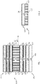
FIG. 1 schematically depicts a photovoltaic device according to one or more embodiments shown and described herein; -
FIG. 2 schematically depicts a substrate according to one or more embodiments shown and described herein; -
FIG. 3 schematically depicts a photovoltaic device according to one or more embodiments shown and described herein; -
FIGS. 4 and5 schematically depict partially formed photovoltaic devices according to one or more embodiments shown and described herein; and -
FIG. 6 schematically depicts a method for performing an alkali and reduced-ambient heat treatment according to one or more embodiments shown and described herein. - Embodiments of a photovoltaic device for generating electrical power from light are described herein. The photovoltaic device generally includes an absorber layer formed from a semiconductor material. The absorber layer can be subjected to one or more processing steps configured to activate the dopant. As used herein, activate or activation can mean manipulating a dopant such that the dopant operates as a charge carrier within a semiconductor, e.g., activated p-type dopants operate as acceptors. Various embodiments of the photovoltaic device and methods for activating the dopants of the absorber layer of the photovoltaic device will be described in more detail herein.
- Referring now to
FIG. 1 , an embodiment of aphotovoltaic device 100 is schematically depicted. Thephotovoltaic device 100 can be configured to receive light and transform light into electrical signals, e.g., photons can be absorbed from the light and transformed into electrical signals via the photovoltaic effect. Accordingly, thephotovoltaic device 100 can define anenergy side 102 configured to be exposed to a light source such as, for example, the sun. Thephotovoltaic device 102 can also define anopposing side 104 offset from theenergy side 102. It is noted that the term "light" can refer to various wavelengths of the electromagnetic spectrum such as, but not limited to, wavelengths in the ultraviolet (UV), infrared (IR), and visible portions of the electromagnetic spectrum. Thephotovoltaic device 100 can include a plurality of layers disposed between theenergy side 102 and theopposing side 104. As used herein, the term "layer" refers to a thickness of material provided upon a surface. Each layer can cover all or any portion of the surface. - The
photovoltaic device 100 can include asubstrate 110 configured to facilitate the transmission of light into thephotovoltaic device 100. Thesubstrate 110 can be disposed at theenergy side 102 of thephotovoltaic device 100. Referring collectively toFIGS. 1 and 2 , thesubstrate 110 can have afirst surface 112 substantially facing theenergy side 102 of thephotovoltaic device 100 and asecond surface 114 substantially facing theopposing side 104 of thephotovoltaic device 100. One or more layers of material can be disposed between thefirst surface 112 and thesecond surface 114 of thesubstrate 110. - The
substrate 110 can include atransparent layer 120 having afirst surface 122 substantially facing theenergy side 102 of thephotovoltaic device 100 and asecond surface 124 substantially facing theopposing side 104 of thephotovoltaic device 100. In some embodiments, thesecond surface 124 of thetransparent layer 120 can form thesecond surface 114 of thesubstrate 110. Thetransparent layer 120 can be formed from a substantially transparent material such as, for example, glass. Suitable glass can include soda-lime glass, or any glass with reduced iron content. Thetransparent layer 120 can have any suitable transmittance, including about 450 nm to about 800 nm in some embodiments. Thetransparent layer 120 may also have any suitable transmission percentage, including, for example, more than about 50% in one embodiment, more than about 60% in another embodiment, more than about 70% in yet another embodiment, more than about 80% in a further embodiment, or more than about 85% in still a further embodiment. In one embodiment,transparent layer 120 can be formed from a glass with about 90% transmittance. Optionally, thesubstrate 110 can include acoating 126 applied to thefirst surface 122 of thetransparent layer 120. Thecoating 126 can be configured to interact with light or to improve durability of thesubstrate 110 such as, but not limited to, an antireflective coating, an antisoiling coating, or a combination thereof. - Referring again to
FIG. 1 , thephotovoltaic device 100 can include abarrier layer 130 configured to mitigate diffusion of contaminants (e.g. sodium) from thesubstrate 110, which could result in degradation or delamination. Thebarrier layer 130 can have afirst surface 132 substantially facing theenergy side 102 of thephotovoltaic device 100 and asecond surface 134 substantially facing theopposing side 104 of thephotovoltaic device 100. In some embodiments, thebarrier layer 130 can be provided adjacent to thesubstrate 110. For example, thefirst surface 132 of thebarrier layer 130 can be provided upon thesecond surface 114 of thesubstrate 100. The phrase "adjacent to," as used herein, means that two layers are disposed contiguously and without any intervening materials between at least a portion of the layers. - Generally, the
barrier layer 130 can be substantially transparent, thermally stable, with a reduced number of pin holes and having high sodium-blocking capability, and good adhesive properties. Alternatively or additionally, thebarrier layer 130 can be configured to apply color suppression to light. Thebarrier layer 130 can include one or more layers of suitable material, including, but not limited to, tin oxide, silicon dioxide, aluminum-doped silicon oxide, silicon oxide, silicon nitride, or aluminum oxide. Thebarrier layer 130 can have any suitable thickness bounded by thefirst surface 132 and thesecond surface 134, including, for example, more than about 500 Å in one embodiment, more than about 750 Å in another embodiment, or less than about 1200 Å in a further embodiment. - Referring still to
FIG. 1 , thephotovoltaic device 100 can include a transparent conductive oxide (TCO)layer 140 configured to provide electrical contact to transport charge carriers generated by thephotovoltaic device 100. TheTCO layer 140 can have afirst surface 142 substantially facing theenergy side 102 of thephotovoltaic device 100 and asecond surface 144 substantially facing theopposing side 104 of thephotovoltaic device 100. In some embodiments, theTCO layer 140 can be provided adjacent to thebarrier layer 130. For example, thefirst surface 142 of theTCO layer 140 can be provided upon thesecond surface 134 of thebarrier layer 130. Generally, theTCO layer 140 can be formed from one or more layers of n-type semiconductor material that is substantially transparent and has a wide band gap. Specifically, the wide band gap can have a larger energy value compared to the energy of the photons of the light, which can mitigate undesired absorption of light. TheTCO layer 140 can include one or more layers of suitable material, including, but not limited to, tin dioxide, doped tin dioxide (e.g., F-SnO2), indium tin oxide, or cadmium stannate. - The
photovoltaic device 100 can include abuffer layer 150 configured to provide an insulating layer between theTCO layer 140 and any adjacent semiconductor layers. Thebuffer layer 150 can have afirst surface 152 substantially facing theenergy side 102 of thephotovoltaic device 100 and asecond surface 154 substantially facing the opposingside 104 of thephotovoltaic device 100. In some embodiments, thebuffer layer 150 can be provided adjacent to theTCO layer 140. For example, thefirst surface 152 of thebuffer layer 150 can be provided upon thesecond surface 144 of theTCO layer 140. Thebuffer layer 140 may include material having higher resistivity than the TCO later 140, including, but not limited to, intrinsic tin dioxide, zinc magnesium oxide (e.g., Zn1-xMgxO), silicon dioxide (SnO2), aluminum oxide (Al2O3), aluminum nitride (AlN), zinc tin oxide, zinc oxide, tin silicon oxide, or any combination thereof. In some embodiments, the material of thebuffer layer 140 can be configured to substantially match the band gap of an adjacent semiconductor layer (e.g., an absorber). Thebuffer layer 150 may have any suitable thickness between thefirst surface 152 and thesecond surface 154, including, for example, more than about 100 Å in one embodiment, between about 100 Å and about 800 Å in another embodiment, or between about 150 Å and about 600 Å in a further embodiment. - Referring again to
FIG. 1 , thephotovoltaic device 100 can include anabsorber layer 160 configured to cooperate with another layer and form a p-n junction within thephotovoltaic device 100. Accordingly, absorbed photons of the light can free electron-hole pairs and generate carrier flow, which can yield electrical power. Theabsorber layer 160 can have afirst surface 162 substantially facing theenergy side 102 of thephotovoltaic device 100 and asecond surface 164 substantially facing the opposingside 104 of thephotovoltaic device 100. A thickness of theabsorber layer 160 can be defined between thefirst surface 162 and thesecond surface 164. The thickness of theabsorber layer 160 can be between about 0.5 µm to about 10 µm such as, for example, between about 1 µm to about 7 µm in one embodiment, or between about 2 µm to about 5 µm in another embodiment. - According to the embodiments described herein, the
absorber layer 160 can be formed from a p-type semiconductor material having an excess of positive charge carriers, i.e., holes or acceptors. Theabsorber layer 160 can include any suitable p-type semiconductor material such as group II-VI semiconductors. Specific examples include, but are not limited to, semiconductor materials comprising from cadmium, tellurium, selenium, or any combination thereof. Suitable examples include, but are not limited to, cadmium telluride, ternaries of cadmium, selenium and tellurium (e.g., CdSexTe1-x,), or quaternaries comprising cadmium, selenium and tellurium. In embodiments where theabsorber layer 160 comprises selenium and cadmium, the atomic percent of the selenium can be greater than about 0 atomic percent and less than about 20 atomic percent. In embodiments where theabsorber layer 160 comprises tellurium and cadmium, the atomic percent of the tellurium can be greater than about 30 atomic percent and less than about 50 atomic percent. It is noted that the atomic percent described herein is representative of the entirety of theabsorber layer 160, the atomic percentage of material at a particular location within theabsorber layer 160 can vary with thickness compared to the overall composition of theabsorber layer 160. It is noted that the concentration of tellurium, selenium, or both can vary through the thickness of theabsorber layer 160. For example, when theabsorber layer 160 comprises a ternary of cadmium, selenium, and tellurium (CdSexTe1-x), x can vary in theabsorber layer 160 with distance from thefirst surface 162 of theabsorber layer 160. In some embodiments, the value of x can decrease in theabsorber layer 160 with distance from thefirst surface 162 of theabsorber layer 160. - According to the embodiments provided herein, the dopant within the
absorber layer 160 can be activated to a desired charge carrier concentration. In some embodiments, theabsorber layer 160 can be doped with a group V dopant such as, for example, nitrogen (N), phosphorous (P), arsenic (As), antimony (Sb), bismuth (Bi), ununpentium (Uup), or a combination thereof. The total dosage of the dopant within theabsorber layer 160 can be controlled. In some embodiments, an atomic concentration of Group V dopant in acentral region 166 theabsorber layer 160 can be greater than about 1×1017cm-3 such as, for example, between about 1×1017cm-3 and about 5×1020cm-3 in one embodiment, between about 3×1017cm-3 and about 1×1019cm-3 in another embodiment, or between about 5×1017cm-3 and about 5×1018cm-3 in a further embodiment. Thecentral region 166 is the middle 50% of theabsorber layer 160, which is offset by 25% of the thickness of theabsorber layer 160 from each of thefirst surface 162 and thesecond surface 164 of theabsorber layer 160. Alternatively or additionally, the concentration profile of the group V dopant can vary through the thickness of theabsorber layer 160. Specifically, the amount of the group V dopant can vary with distance from thefirst surface 162 of theabsorber layer 160. - Referring still to
FIG. 1 , the p-n junction can be formed by providing theabsorber layer 160 sufficiently close to a portion of thephotovoltaic device 100 having an excess of negative charge carriers, i.e., electrons or donors. In some embodiments, theabsorber layer 160 can be provided adjacent to n-type semiconductor material. Alternatively, one or more intervening layers can be provided between theabsorber layer 160 and n-type semiconductor material. In some embodiments, theabsorber layer 160 can be provided adjacent to thebuffer layer 150. For example, thefirst surface 162 of theabsorber layer 160 can be provided upon thesecond surface 154 of thebuffer layer 150. - Referring now to
FIG. 3 , in some embodiments, aphotovoltaic device 200 can include awindow layer 170 comprising n-type semiconductor material. Aside from thewindow layer 170, thephotovoltaic device 200 can have a substantially similar layer structure as the photovoltaic device 100 (FIG. 1 ). Theabsorber layer 160 can be formed adjacent to thewindow layer 170. Thewindow layer 170 can have afirst surface 172 substantially facing theenergy side 102 of thephotovoltaic device 200 and asecond surface 174 substantially facing the opposingside 104 of thephotovoltaic device 200. In some embodiments, thewindow layer 170 can be positioned between theabsorber layer 160 and theTCO layer 140. In one embodiment, thewindow layer 170 can be positioned between theabsorber layer 160 and thebuffer layer 150. Thewindow layer 170 can include any suitable material, including, for example, cadmium sulfide, zinc sulfide, cadmium zinc sulfide, zinc magnesium oxide, or any combination thereof. - Referring again to
FIG. 1 , thephotovoltaic device 100 can include aback contact layer 180 configured to mitigate undesired alteration of the dopant and to provide electrical contact to theabsorber layer 160. Theback contact layer 180 can have afirst surface 182 substantially facing theenergy side 102 of thephotovoltaic device 100 and asecond surface 184 substantially facing the opposingside 104 of thephotovoltaic device 100. A thickness of theback contact layer 180 can be defined between thefirst surface 182 and thesecond surface 184. The thickness of theback contact layer 180 can be between about 5 nm to about 200 nm such as, for example, between about 10 nm to about 50 nm in one embodiment. - In some embodiments, the
back contact layer 180 can be provided adjacent to theabsorber layer 160. For example, thefirst surface 182 of theback contact layer 180 can be provided upon thesecond surface 164 of theabsorber layer 160. In some embodiments, theback contact layer 180 can include binary or ternary combinations of materials from groups I, II, VI, such as for example, one or more layers containing zinc, copper, cadmium and tellurium in various compositions. Further exemplary materials include, but are not limited to, zinc telluride doped with copper telluride, or zinc telluride alloyed with copper telluride. - The
photovoltaic device 100 can include aconducting layer 190 configured to provide electrical contact with theabsorber layer 160. Theconducting layer 190 can have afirst surface 192 substantially facing theenergy side 102 of thephotovoltaic device 100 and asecond surface 194 substantially facing the opposingside 104 of thephotovoltaic device 100. In some embodiments, theconducting layer 190 can be provided adjacent to theback contact layer 180. For example, thefirst surface 192 of theconducting layer 190 can be provided upon thesecond surface 184 of theback contact layer 180. Theconducting layer 190 can include any suitable conducting material such as, for example, one or more layers of nitrogen-containing metal, silver, nickel, copper, aluminum, titanium, palladium, chrome, molybdenum, gold, or the like. Suitable examples of a nitrogen-containing metal layer can include aluminum nitride, nickel nitride, titanium nitride, tungsten nitride, selenium nitride, tantalum nitride, or vanadium nitride. - The
photovoltaic device 100 can include aback support 196 configured to cooperate with thesubstrate 110 to form a housing for thephotovoltaic device 100. Theback support 196 can be disposed at the opposingside 102 of thephotovoltaic device 100. For example, theback support 196 can be formed adjacent to conductinglayer 190. Theback support 196 can include any suitable material, including, for example, glass (e.g., soda-lime glass). - Referring collectively to
FIGS. 1 and3 , manufacturing of aphotovoltaic device - Referring collectively to
FIGS. 4 and5 , a layer of a partially formed device can be processed. In some embodiments, a partially formedphotovoltaic device 202 can comprise theabsorber layer 160 adjacent to alayer stack 204. Thelayer stack 204 can include one or more of the layers of thephotovoltaic device 100, 200 (FIGS. 1 and3 ) disposed between theabsorber layer 160 and theenergy side 102. Alternatively, a partially formed photovoltaic device 206 can comprise theabsorber layer 160 adjacent to alayer stack 208. Thelayer stack 208 can include one or more of the layers of thephotovoltaic device 100, 200 (FIGS. 1 and3 ) between theabsorber layer 160 and the opposingside 104. - Referring now to
FIG. 6 , amethod 210 for performing an alkali and reduced-ambient heat treatment (ARHT) is depicted. The ARHT is an annealing process that employs a chemical compound and a reducing atmosphere. In some embodiments, theabsorber layer 160 can be doped with a group V dopant prior to being subjected to the ARHT. The ARHT can be used to activate dopants within theabsorber layer 160. As is explained in greater detail herein, the ARHT can activate a larger number of dopants and generate a larger carrier concentration than other heat treatment processes, while providing sufficient grain growth within theabsorber layer 160. - Referring collectively to
FIGS. 4 ,5, and 6 , themethod 200 for performing the ARHT can include aprocess 212 for exposing theabsorber layer 160 to a reducingenvironment 220. Thefirst surface 162 or thesecond surface 164 of theabsorber layer 160 can be subjected to the reducingenvironment 220. The reducingenvironment 220 is an atmospheric condition in which oxidation is mitigated by removal of oxygen and other oxidizing gases or vapors, i.e., the reducing environment can be substantially free of substances tending to oxidize the Group V dopants. Additionally, the reducingenvironment 220 can include a forming gas configured to mitigate the formation of group V oxides. The forming gas can be energetically more favorable to oxidation than the group V dopant, i.e., an oxidation reaction of the forming gas during the ARHT can have a more negative Gibbs free energy change (ΔG) than the group V dopant. - In some embodiments, the forming gas can comprise hydrogen, nitrogen, or combinations thereof. In one embodiment, the forming gas consists essentially of a mixture of H2 and N2. For example, the forming gas can comprise a mixture of about 50.0 to 99.4% N2 and about 0.6 to 3.0% H2. Alternatively, the forming gas can comprise H2 in an atomic fraction range of 0.5-100%. Thus, the reducing
environment 220 can comprise a forming gas consisting essentially of 100% H2. Other suitable reducing agents can include methane (CH4), carbon monoxide (CO), hydrogen sulfide (H2S), and ammonia compounds (NH3). In some embodiments, the reducingenvironment 220 can be provided within aprocessing chamber 222 configured to substantially prevent the inclusion of substances tending to oxidize Group V dopants within the reducingenvironment 220. Accordingly, in some embodiments, the reducingenvironment 220 can consist essentially of the forming gas. Alternatively or additionally, theprocessing chamber 222 can be configured to maintain partial vacuum pressure. Accordingly, the reducingenvironment 220 can be provided at a vacuum pressure in a range of about 200 Torr to about 800 Torr such as, for example, in a range of about 3 Torr to about 50 Torr. - The
method 200 for performing the ARHT can include aprocess 214 for contacting theabsorber layer 160 with anannealing compound 224. In some embodiments, theannealing compound 224 can be applied to thefirst surface 162 or thesecond surface 164 of theabsorber layer 160 as a solution. For example, theannealing compound 224 can be sprayed, spin coated, or roll coated upon theabsorber layer 160. Alternatively or additionally, theannealing compound 224 can be supplied as a vapor in theprocessing chamber 222. Theannealing compound 224 comprises a combination of cadmium chloride (CdCl2) and one or more alkali metal chloride. The alkali metal chlorides can be formed from an alkali metal such as, for example, lithium (Li), sodium (Na), potassium (K), rubidium (Rb), cesium (Cs), and francium (Fr). Suitable alkali metal chlorides include, but are not limited to, LiCl, NaCl, KCl, RbCl, or combinations thereof. The composition of theannealing compound 224 is controlled such that a desired ratio of cadmium to alkali metal is maintained. Generally, theannealing compound 224 includes much more cadmium than alkali metal as measured by atomic ratio. For example, the desired ratio of cadmium to alkali metal is less than about 10,000 parts per million (ppm) such as, for example, between about 500 ppm to about 6,000 ppm in one embodiment, between about 750 ppm to about 4,500 ppm in another embodiment, or between about 1,000 ppm and about 3,000 ppm in a further embodiment. - The
method 200 for performing the ARHT can include aprocess 216 for annealing theabsorber layer 160 in the reducingenvironment 220. Generally, annealing includes heating the absorber layer 160 (e.g., polycrystalline semiconductor material) for sufficient time and temperature to facilitate re-crystallization of theabsorber layer 160. For example, theabsorber layer 160 can be processed at a temperature between about 350° C and about 500° C for between about 5 minutes and about 60 minutes such as, for example, at a temperature in a range of about 400° C to about 500° C for a duration of about 10 minutes to about 55 minutes, in one embodiment, or at a temperature in a range of about 400° C to about 450° C for a duration of about 15 minutes to about 50 minutes, in another embodiment. It is noted that, whileprocess 212,process 214, andprocess 216 may be depicted in a sequential manner inFIG. 6 , the embodiments provided herein are not limited to any particular order ofprocess 212,process 214, andprocess 216. In some embodiments, a surface of theabsorber layer 160 can be initially contacted with theannealing compound 224 while in the reducingenvironment 220, and during annealing. In other embodiments, a surface of theabsorber layer 160 can be contacted with theannealing compound 224 and subsequently placed in the reducingenvironment 220 and annealed. In some embodiments, each ofprocess 212,process 214, andprocess 216 can be performed contemporaneously, i.e., theannealing compound 224 can remain in contact with theabsorber layer 160 for at least a portion of the annealing in the reducingenvironment 220. - In addition to recrystallization of the
absorber layer 160, which can be formed from polycrystalline semiconductors, the ARHT can result in grain growth in theabsorber layer 160. Moreover, the constituents (e.g., alkali metal, chlorine, or both) of theannealing compound 224 can diffuse intoabsorber layer 160 and impact the activation of group V dopants present in the absorber layer. As is explained in greater detail herein, the diffusion of constituents of theannealing compound 224 into other layers of thelayer stack 204, 206 can impact the overall device efficiency. - Referring again to
FIGS. 1 and3 , after ARHT, theabsorber layer 160 can comprise a relatively high carrier concentration compared to previously known processes such as, for example, CHT. For Cu-doped CdTe absorber devices subjected to CHT, the nominal carrier concentration can often be below about 1×1015cm-3. In contrast, absorber layers 160 of the present disclosure such as, for example, absorber layers 160 with group V dopants and comprising cadmium and tellurium or cadmium, selenium and tellurium, achieve carrier concentrations in theabsorber layer 160 greater than about 4×1015cm-3. In some embodiments, the carrier concentration of theabsorber layer 160 is greater than about 8×1015cm-3 such as, for example, greater than about 1×1016cm-3 in one embodiment, or between about 8×1015cm-3 and about 6×1016cm-3 in another embodiment. - As is noted above, ARHT is performed in a reducing
environment 220 to reduce the presence of oxygen. However, in some embodiments, oxygen can diffuse into thecentral region 166 of theabsorber layer 160. In such embodiments, thecentral region 166 of theabsorber layer 160 can have an alkali to oxygen ratio, i.e., the ratio of the atomic concentration of an alkali metal to the atomic concentration of oxygen at the measured depth, in a desired range. The alkali to oxygen ratio can be at least 0.1 in thecentral region 166 of theabsorber layer 160 such as for example, an alkali to oxygen ratio of at least 0.75 in one embodiment, an alkali to oxygen ratio of at least 5 in another embodiment, an alkali to oxygen ratio of between about 10 and about 1,000 in a further embodiment, or an alkali to oxygen ratio of between about 10 and about 100 in yet another embodiment. - According to the embodiments provided herein, the atomic concentration of the alkali metal in the absorber layer can be greater than about 1×1016cm-3. In some embodiments, the atomic concentration of alkali metal in the
absorber layer 160 is greater than about 2×1016cm-3 such as, for example, greater than about 1×1017cm-3 in one embodiment, or between about 5×1016cm-3 and about 1×1019cm-3 in another embodiment. The alkali metal can further diffuse into other layers of thephotovoltaic device TCO layer 140. Generally, the atomic concentration of the alkali metal in theTCO layer 140 is greater than the atomic concentration of the alkali metal in theabsorber layer 160. - Applicant has discovered that excessive concentration of the alkali metal is correlated to degradation of the sheet resistance of the
TCO layer 140. Accordingly, an alkali metal ratio between theTCO layer 140 and theabsorber layer 160, i.e., ratio of the atomic concentration of alkali metal in theTCO layer 140 to the atomic concentration of the alkali metal in theabsorber layer 160 can be controlled. In some embodiments, the alkali metal ratio between theTCO layer 140 and theabsorber layer 160 can be less than about 1,000 such as, for example, less than about 500 in one embodiment, or less than about 100 in another embodiment. Applicant has further discovered that potassium (K) and rubidium (Rb) have demonstrated improved performance with respect to sheet resistance compared to other alkali metals. Indeed, the presence of potassium (K) and rubidium (Rb) has demonstrated improved performance compared to cadmium chloride based annealing compounds without any alkali metals. Accordingly, in some embodiments, the alkali metal can consist of potassium (K), rubidium (Rb), or both.Table 1 Annealing Compound Alkali Concentration (ppm) Eff (%) Carrier concentration Comparative Example CdCl2 0 10 3×1015cm-3 Example 1 CdCl2 + LiCl 3000 11 4×1015cm-3 Example 2 CdCl2 + LiCl + KCl 3000 16.5 4×1015cm-3 Example 3 CdCl2 + KCl 2000 18 2×1016cm-3 Example 4 CdCl2 + KCl 3000 17.5 2×1016cm-3 Example 5 CdCl2 + RbCl 1000 16 8×1015cm-3 Example 6 CdCl2 + RbCl 2000 18.2 1.5×1016cm-3 Example 7 CdCl2 + RbCl 3000 17 4.5×1016cm-3 - Referring above to Table 1, the annealing compound column of Table 1 summarizes the presence of cadmium chloride and alkali metal chlorides in the annealing compound. The alkali concentration column summarizes the atomic ratio of cadmium to alkali metal in parts per million in the annealing compound. Each of Comparative Example and Examples 1-7 were processed with similar annealing compounds with the differences summarized in the annealing compound and alkali concentration columns of Table 1. Accordingly, Examples 1-7 were processed according to the ARHT process described herein. Comparative Example 1 can be considered analogous to a CHT process, except the CHT was performed in a reducing atmosphere. The efficiency column summarizes the measured efficiency of photovoltaic devices with absorber layers processed as summarized in Table 1, and after device integration. The absorber layers of the compounds were substantially similar and comprised cadmium and tellurium. Each of the absorber layers were doped with about 1×1018cm-3 of arsenic (As), which was verified using dynamic secondary ion mass spectrometry (SIMS). The carrier concentration column summarizes the carrier concentration of the absorber layers processed as summarized in Table 1, and after device integration. The carrier concentration numbers were derived from capacitance-voltage (C-V) measurements.
- As summarized above in Table 1, each of Examples 1-7 demonstrated an improvement in efficiency and carrier concentration compared to Comparative Example 1. Additionally, Examples 3-4, which included potassium (K) demonstrated improved efficiency and carrier concentration compared to Examples 1 and 2, which included lithium (Li). Likewise, Examples 6-7, which include rubidium (Rb) demonstrated improved efficiency and carrier concentration compared to Examples 1 and 2.
- It should now be understood that the embodiments provided herein, relate to ARHT methods that enhance Group V doping activation. Photovoltaic devices formed using the ARHT methods described herein demonstrated relatively high carrier concentration. Accordingly, the embodiments provided herein resolve some of the challenges associated with photovoltaic devices having absorber layers that include cadmium and tellurium. Such devices can struggle to achieve high p-type carrier concentration. For Cu-doped CdTe based devices, the nominal carrier concentration can be below 3×1015cm-3, which results in poor device performance (e.g., efficiency).
- Moreover, ARHT methods described herein results in devices having sufficient grain growth in the absorber layer. For example, previously known processes such as, for example, CHT, when performed in a reducing environment, lack sufficient grain growth. Without being bound to theory, it is believed that the due to the lack of oxygen, previously known processes yield absorber layers with small grain and poor carrier concentration stability. The ARHT methods described herein yield desirable grain growth.
- According to the embodiments provided herein, a photovoltaic device can include an absorber layer. The absorber layer can include cadmium, tellurium, and selenium. The absorber layer can be doped p-type with a Group V dopant and can have a carrier concentration of the Group V dopant greater than 4×1015cm-3. The absorber layer can include oxygen in a central region of the absorber layer. The absorber layer can include an alkali metal in the central region of the absorber layer. A ratio of an atomic concentration of the alkali metal to an atomic concentration of the oxygen can be at least 0.1 in the central region of the absorber layer.
- According to the embodiments, a method for carrier activation can include exposing an absorber layer to a reducing environment. The absorber layer can include cadmium, tellurium, selenium, and a Group V dopant. The method for carrier activation can include contacting the absorber layer with an annealing compound. The annealing compound can include cadmium chloride and an alkali metal chloride. The alkali metal chloride can be formed from an alkali metal. An atomic ratio of cadmium to the alkali metal in the annealing compound can be less than 10,000 parts per million. The method for carrier activation can include annealing the absorber layer, whereby at least a portion of the Group V dopant is activated. After the absorber layer is annealed, the absorber layer can have a carrier concentration of the Group V dopant greater than 4×1015cm-3.
- It is noted that the terms "substantially" and "about" may be utilized herein to represent the inherent degree of uncertainty that may be attributed to any quantitative comparison, value, measurement, or other representation. These terms are also utilized herein to represent the degree by which a quantitative representation may vary from a stated reference without resulting in a change in the basic function of the subject matter at issue.
- While particular embodiments have been illustrated and described herein, it should be understood that various other changes and modifications may be made without departing from the spirit and scope of the claimed subject matter. Moreover, although various aspects of the claimed subject matter have been described herein, such aspects need not be utilized in combination. It is therefore intended that the appended claims cover all such changes and modifications that are within the scope of the claimed subject matter.
- Various preferred features and embodiments of the present invention will now be described with reference to the following numbered paragraphs (paras).
- 1. A photovoltaic device comprising an absorber layer, wherein:
- the absorber layer comprises cadmium, tellurium, and selenium;
- the absorber layer is doped p-type with a Group V dopant and has a carrier concentration of the Group V dopant greater than 4×1015cm-3;
- the absorber layer comprises oxygen in a central region of the absorber layer;
- the absorber layer comprises an alkali metal in the central region of the absorber layer; and
- a ratio of an atomic concentration of the alkali metal to an atomic concentration of the oxygen is at least 0.1 in the central region of the absorber layer.
- 2. The photovoltaic device of para 1, wherein the alkali metal is potassium.
- 3. The photovoltaic device of para 1, wherein the alkali metal is rubidium.
- 4. The photovoltaic device of para 1, wherein the carrier concentration of the Group V dopant is between 8×1015cm-3 and 6×1016cm-3.
- 5. The photovoltaic device of para 4, wherein an atomic concentration of the Group V dopant in the central region of the absorber layer is greater than 1×1017cm-3.
- 6. The photovoltaic device of para 1, comprising a transparent conductive oxide layer disposed between the absorber layer and an energy side of the photovoltaic device, wherein the transparent conductive oxide layer comprises the alkali metal.
- 7. The photovoltaic device of para 6, wherein an atomic concentration of the alkali metal in the transparent conductive oxide layer is greater than the atomic concentration of the alkali metal in the central region of the absorber layer.
- 8. The photovoltaic device of
para 7, wherein an alkali metal ratio of the atomic concentration of the alkali metal in the transparent conductive oxide layer to the atomic concentration of the alkali metal in the central region of the absorber layer is less than 1,000. - 9. A method for carrier activation, comprising:
- exposing an absorber layer to a reducing environment, wherein the absorber layer comprises cadmium, tellurium, selenium, and a Group V dopant;
- contacting the absorber layer with an annealing compound, wherein:
- the annealing compound comprises cadmium chloride and an alkali metal chloride;
- the alkali metal chloride is formed from an alkali metal;
- an atomic ratio of cadmium to the alkali metal in the annealing compound is less than 10,000 parts per million; and
- annealing the absorber layer, whereby at least a portion of the Group V dopant is activated, and wherein, after the absorber layer is annealed, the absorber layer has a carrier concentration of the Group V dopant greater than 4×1015cm-3.
- 10. The method of para 9, wherein the reducing environment comprises a forming gas configured to mitigate formation of group V oxides, the forming gas comprising hydrogen, nitrogen, or combinations thereof.
- 11. The method of para 9, wherein the reducing environment is at a vacuum pressure between 200 Torr and 800 Torr.
- 12. The method of para 9, wherein the absorber layer is annealed at a temperature between 350° C and 500° C for between 5 minutes and 60 minutes.
- 13. The method of para 9, wherein the alkali metal chloride comprises LiCl, KCl, RbCl, or combinations thereof.
- 14. The method of para 9, wherein the atomic ratio of the cadmium to the alkali metal in the annealing compound is between 500 parts per million and 6,000 parts per million.
- 15. The method of para 14, wherein the alkali metal is potassium.
- 16. The method of para 14, wherein the alkali metal is rubidium.
- 17. The method of para 9, wherein, after the absorber layer is annealed, the absorber layer has a carrier concentration of the Group V dopant between 8×1015cm-3 and 6×1016cm-3.
- 18. The method of para 17, wherein an atomic concentration of the Group V dopant in the absorber layer is greater than 1×1017cm-3.
- 19. The photovoltaic device of any of paras 1 to 3, wherein the carrier concentration of the Group V dopant is between 8×1015cm-3 and 6×1016cm-3.
- 20. The photovoltaic device of any of paras 1 to 3 and 19, wherein an atomic concentration of the Group V in the central region of the absorber layer is greater than 1×1017cm-3.
- 21. The photovoltaic device of any of paras 1 to 3 and 19 to 20, comprising a transparent conductive oxide layer disposed between the absorber layer and an energy side of the photovoltaic device, wherein the transparent conductive oxide layer comprises the alkali metal.
- 22. The photovoltaic device of para 21, wherein an atomic concentration of the alkali metal in the transparent conductive oxide layer is greater than the atomic concentration of the alkali metal in the central region of the absorber layer.
- 23. The photovoltaic device of para 22, wherein an alkali metal ratio of the atomic concentration of the alkali metal in the transparent conductive oxide layer to the atomic concentration of the alkali metal in the central region of the absorber layer is less than 1,000.
- 24. The method of any of paras 9 to 10, wherein the reducing environment is at a vacuum pressure between 200 Torr and 800 Torr.
- 25. The method of any of paras 9 to 10 and 24, wherein the absorber layer is annealed at a temperature between 350° C and 500° C for between 5 minutes and 60 minutes.
- 26. The method of any of paras 9 to 10 and 24 to 25, wherein the alkali metal chloride comprises LiCl, KCl, RbCl, or combinations thereof.
- 27. The method of any of paras 9 to 10 and 24 to 26, wherein the atomic ratio of the cadmium to the alkali metal in the annealing compound is between 500 parts per million and 6,000 parts per million.
- 28. The method of any of paras 9 to 10 and 24 to 27, wherein the alkali metal is potassium.
- 29. The method of any of paras 9 to 10 and 24 to 27, wherein the alkali metal is rubidium.
- 30. The method of any of paras 9 to 10 and 24 to 29, wherein, after the absorber layer is annealed, the absorber layer has a carrier concentration of the Group V dopant between 8×1015cm-3 and 6×1016cm-3.
- 31. The method of any of paras 9 to 10 and 24 to 30, wherein an atomic concentration of the Group V in the absorber layer is greater than 1×1017cm-3.
- 32. The method of para 31, wherein the carrier concentration of the Group V dopant is between 8×1015cm-3 and 6×1016cm-3.
Claims (10)
- A method for carrier activation, comprising:exposing an absorber layer (160) to a reducing environment (220), wherein the absorber layer comprises cadmium, tellurium, selenium, and a Group V dopant;contacting the absorber layer (160) with an annealing compound (224), wherein:the annealing compound (224) comprises cadmium chloride and an alkali metal chloride;the alkali metal chloride comprises an alkali metal;an atomic ratio of alkali metal to cadmium in the annealing compound (224) is less than 10,000 parts per million; andannealing the absorber layer (160) in the reducing environment (220), whereby at least a portion of the Group V dopant is activated, and wherein, after the absorber layer is annealed, the absorber layer (160) has a carrier concentration of the Group V dopant greater than 4×1015cm-3.
- The method of claim 1, wherein the reducing environment (220) comprises a forming gas configured to mitigate formation of group V oxides, the forming gas comprising hydrogen, nitrogen, or combinations thereof.
- The method of claim 1 or claim 2, wherein the reducing environment (220) is at a vacuum pressure between 200 Torr and 800 Torr.
- The method of any preceding claim, wherein the absorber layer (160) is annealed at a temperature between 350° C and 500° C for between 5 minutes and 60 minutes.
- The method of any preceding claim, wherein the alkali metal chloride comprises LiCl, KCl, RbCl, or combinations thereof.
- The method of any preceding claim, wherein the atomic ratio of alkali metal to cadmium in the annealing compound (224) is between 500 parts per million and 6,000 parts per million.
- The method of any preceding claim, wherein the alkali metal is potassium.
- The method of claims 1 to 6, wherein the alkali metal is rubidium.
- The method of any preceding claim, wherein, after the absorber layer (160) is annealed, the absorber layer has a carrier concentration of the Group V dopant between 8×1015cm-3 and 6×1016cm-3.
- The method of claim 9, wherein an atomic concentration of the Group V dopant in the absorber layer (160) is greater than 1×1017cm-3.
Priority Applications (1)
| Application Number | Priority Date | Filing Date | Title |
|---|---|---|---|
| EP22155897.6A EP4020603A1 (en) | 2017-12-07 | 2017-12-07 | Method for forming a photovoltaic device with group v dopants |
Applications Claiming Priority (3)
| Application Number | Priority Date | Filing Date | Title |
|---|---|---|---|
| EP17934240.7A EP3721479B1 (en) | 2017-12-07 | 2017-12-07 | Photovoltaic device with group v dopants and method for forming the same |
| EP22155897.6A EP4020603A1 (en) | 2017-12-07 | 2017-12-07 | Method for forming a photovoltaic device with group v dopants |
| PCT/CN2017/114980 WO2019109297A1 (en) | 2017-12-07 | 2017-12-07 | Photovoltaic devices and semiconductor layers with group v dopants and methods for forming the same |
Related Parent Applications (1)
| Application Number | Title | Priority Date | Filing Date |
|---|---|---|---|
| EP17934240.7A Division EP3721479B1 (en) | 2017-12-07 | 2017-12-07 | Photovoltaic device with group v dopants and method for forming the same |
Publications (1)
| Publication Number | Publication Date |
|---|---|
| EP4020603A1 true EP4020603A1 (en) | 2022-06-29 |
Family
ID=66750043
Family Applications (2)
| Application Number | Title | Priority Date | Filing Date |
|---|---|---|---|
| EP17934240.7A Active EP3721479B1 (en) | 2017-12-07 | 2017-12-07 | Photovoltaic device with group v dopants and method for forming the same |
| EP22155897.6A Pending EP4020603A1 (en) | 2017-12-07 | 2017-12-07 | Method for forming a photovoltaic device with group v dopants |
Family Applications Before (1)
| Application Number | Title | Priority Date | Filing Date |
|---|---|---|---|
| EP17934240.7A Active EP3721479B1 (en) | 2017-12-07 | 2017-12-07 | Photovoltaic device with group v dopants and method for forming the same |
Country Status (6)
| Country | Link |
|---|---|
| US (2) | US11502212B2 (en) |
| EP (2) | EP3721479B1 (en) |
| JP (1) | JP7046184B2 (en) |
| CN (1) | CN111670504B (en) |
| MY (2) | MY207983A (en) |
| WO (1) | WO2019109297A1 (en) |
Families Citing this family (9)
| Publication number | Priority date | Publication date | Assignee | Title |
|---|---|---|---|---|
| WO2009058985A1 (en) | 2007-11-02 | 2009-05-07 | First Solar, Inc. | Photovoltaic devices including doped semiconductor films |
| AU2018225659B2 (en) | 2017-02-24 | 2023-02-02 | First Solar, Inc. | Doped photovoltaic semiconductor layers and methods of making |
| EP3719853B1 (en) | 2017-02-27 | 2025-10-15 | First Solar, Inc. | Thin-film photovoltaic devices including cadmium and tellurium doped with group v elements |
| MY207983A (en) | 2017-12-07 | 2025-03-31 | First Solar Inc | Photovoltaic devices and semiconductor layers with group v dopants and methods for forming the same |
| MY203478A (en) | 2018-02-01 | 2024-06-28 | First Solar Inc | Methods for group v doping of photovoltaic devices |
| CN113261116B (en) | 2018-10-24 | 2024-10-11 | 第一阳光公司 | Buffer layer for photovoltaic devices with group V doping |
| US11302840B2 (en) * | 2018-10-30 | 2022-04-12 | Vandette B. Carter | Solar cell with three layers and forward biasing voltage |
| WO2025221484A1 (en) * | 2024-04-05 | 2025-10-23 | First Solar, Inc. | Photovoltaic devices with semiconductor contact layers |
| WO2025213414A1 (en) * | 2024-04-11 | 2025-10-16 | China Triumph International Engineering Co., Ltd. | Photovoltaic device and method therefor |
Citations (5)
| Publication number | Priority date | Publication date | Assignee | Title |
|---|---|---|---|---|
| CN102810598A (en) * | 2012-07-31 | 2012-12-05 | 江苏顺风光电科技有限公司 | Solar cell homogenizing annealing process |
| US20140326315A1 (en) * | 2013-05-02 | 2014-11-06 | First Solar, Inc. | Photovoltaic devices and method of making |
| US20140360565A1 (en) * | 2013-06-07 | 2014-12-11 | First Solar, Inc. | Photovoltaic devices and method of making |
| US20140373908A1 (en) * | 2013-06-21 | 2014-12-25 | First Solar Inc. | Photovoltaic devices |
| US20160126396A1 (en) * | 2014-11-03 | 2016-05-05 | First Solar, Inc. | Photovoltaic devices and method of manufacturing |
Family Cites Families (26)
| Publication number | Priority date | Publication date | Assignee | Title |
|---|---|---|---|---|
| US4950615A (en) * | 1989-02-06 | 1990-08-21 | International Solar Electric Technology, Inc. | Method and making group IIB metal - telluride films and solar cells |
| US5279678A (en) | 1992-01-13 | 1994-01-18 | Photon Energy, Inc. | Photovoltaic cell with thin CS layer |
| US5501744A (en) * | 1992-01-13 | 1996-03-26 | Photon Energy, Inc. | Photovoltaic cell having a p-type polycrystalline layer with large crystals |
| JPH0685297A (en) | 1992-09-03 | 1994-03-25 | Matsushita Electric Ind Co Ltd | Solar cell manufacturing method |
| JP3465872B2 (en) | 1998-09-21 | 2003-11-10 | 松下電池工業株式会社 | Method and apparatus for treating cadmium telluride film for solar cell |
| US9147778B2 (en) | 2006-11-07 | 2015-09-29 | First Solar, Inc. | Photovoltaic devices including nitrogen-containing metal contact |
| US8309387B2 (en) * | 2007-04-13 | 2012-11-13 | David Forehand | Improving back-contact performance of group VI containing solar cells by utilizing a nanoscale interfacial layer |
| WO2009058985A1 (en) | 2007-11-02 | 2009-05-07 | First Solar, Inc. | Photovoltaic devices including doped semiconductor films |
| US8298856B2 (en) * | 2008-07-17 | 2012-10-30 | Uriel Solar, Inc. | Polycrystalline CDTE thin film semiconductor photovoltaic cell structures for use in solar electricity generation |
| US20100273287A1 (en) * | 2009-04-23 | 2010-10-28 | Reel Solar, Inc. | Methods for integrating quantum window structures into solar cells |
| US20130327398A1 (en) * | 2011-02-28 | 2013-12-12 | Alliance For Sustainable Energy, Llc | Thin-Film Photovoltaic Devices and Methods of Manufacture |
| US9608144B2 (en) | 2011-06-01 | 2017-03-28 | First Solar, Inc. | Photovoltaic devices and method of making |
| US9447489B2 (en) * | 2011-06-21 | 2016-09-20 | First Solar, Inc. | Methods of making photovoltaic devices and photovoltaic devices |
| US20130074914A1 (en) * | 2011-09-26 | 2013-03-28 | General Electric Company | Photovoltaic devices |
| EP2805356A2 (en) | 2012-01-17 | 2014-11-26 | First Solar, Inc | Photovoltaic device having an absorber multilayer and method of manufacturing the same |
| US9496446B2 (en) * | 2012-01-31 | 2016-11-15 | First Solar, Inc. | Photovoltaic devices and method of making |
| US9054245B2 (en) * | 2012-03-02 | 2015-06-09 | First Solar, Inc. | Doping an absorber layer of a photovoltaic device via diffusion from a window layer |
| US9147792B2 (en) | 2012-05-21 | 2015-09-29 | First Solar, Inc. | Method of providing chloride treatment for a photovoltaic device and a chloride treated photovoltaic device |
| US8809105B2 (en) * | 2012-06-14 | 2014-08-19 | First Solar, Inc. | Method of processing a semiconductor assembly |
| WO2014121187A2 (en) | 2013-02-01 | 2014-08-07 | First Solar, Inc. | Photovoltaic device including a p-n junction and method of manufacturing |
| CN104183663B (en) | 2013-05-21 | 2017-04-12 | 第一太阳能马来西亚有限公司 | Photovoltaic device and manufacturing method thereof |
| AU2018225659B2 (en) | 2017-02-24 | 2023-02-02 | First Solar, Inc. | Doped photovoltaic semiconductor layers and methods of making |
| EP3719853B1 (en) | 2017-02-27 | 2025-10-15 | First Solar, Inc. | Thin-film photovoltaic devices including cadmium and tellurium doped with group v elements |
| MY207983A (en) | 2017-12-07 | 2025-03-31 | First Solar Inc | Photovoltaic devices and semiconductor layers with group v dopants and methods for forming the same |
| MY203478A (en) | 2018-02-01 | 2024-06-28 | First Solar Inc | Methods for group v doping of photovoltaic devices |
| JP2021510011A (en) | 2018-03-13 | 2021-04-08 | ファースト・ソーラー・インコーポレーテッド | Annealing Material and Method for Annealing Photovoltaic Devices Using Annealing Material |
-
2017
- 2017-12-07 MY MYPI2022007325A patent/MY207983A/en unknown
- 2017-12-07 EP EP17934240.7A patent/EP3721479B1/en active Active
- 2017-12-07 MY MYPI2020002894A patent/MY196698A/en unknown
- 2017-12-07 US US16/770,388 patent/US11502212B2/en active Active
- 2017-12-07 CN CN201780098268.5A patent/CN111670504B/en active Active
- 2017-12-07 WO PCT/CN2017/114980 patent/WO2019109297A1/en not_active Ceased
- 2017-12-07 JP JP2020531089A patent/JP7046184B2/en active Active
- 2017-12-07 EP EP22155897.6A patent/EP4020603A1/en active Pending
-
2022
- 2022-11-14 US US17/986,747 patent/US12356755B2/en active Active
Patent Citations (5)
| Publication number | Priority date | Publication date | Assignee | Title |
|---|---|---|---|---|
| CN102810598A (en) * | 2012-07-31 | 2012-12-05 | 江苏顺风光电科技有限公司 | Solar cell homogenizing annealing process |
| US20140326315A1 (en) * | 2013-05-02 | 2014-11-06 | First Solar, Inc. | Photovoltaic devices and method of making |
| US20140360565A1 (en) * | 2013-06-07 | 2014-12-11 | First Solar, Inc. | Photovoltaic devices and method of making |
| US20140373908A1 (en) * | 2013-06-21 | 2014-12-25 | First Solar Inc. | Photovoltaic devices |
| US20160126396A1 (en) * | 2014-11-03 | 2016-05-05 | First Solar, Inc. | Photovoltaic devices and method of manufacturing |
Also Published As
| Publication number | Publication date |
|---|---|
| EP3721479A4 (en) | 2020-10-14 |
| JP2021509222A (en) | 2021-03-18 |
| MY196698A (en) | 2023-04-30 |
| MY207983A (en) | 2025-03-31 |
| WO2019109297A1 (en) | 2019-06-13 |
| US11502212B2 (en) | 2022-11-15 |
| US20230082990A1 (en) | 2023-03-16 |
| US20200381567A1 (en) | 2020-12-03 |
| JP7046184B2 (en) | 2022-04-01 |
| CN111670504A (en) | 2020-09-15 |
| US12356755B2 (en) | 2025-07-08 |
| EP3721479B1 (en) | 2022-02-16 |
| EP3721479A1 (en) | 2020-10-14 |
| CN111670504B (en) | 2024-01-30 |
Similar Documents
| Publication | Publication Date | Title |
|---|---|---|
| US12356755B2 (en) | Photovoltaic devices and semiconductor layers with group v dopants and methods for forming the same | |
| JP7579930B2 (en) | Doped photovoltaic semiconductor layers and methods of manufacture - Patents.com | |
| EP3747057B1 (en) | Method for group v doping of an absorber layer in photovoltaic devices | |
| US20250120219A1 (en) | Buffer Layers for Photovoltaic Devices with Group V Doping | |
| US20240429329A1 (en) | Layer structures for photovoltaic devices and photovoltaic devices including the same | |
| US20220102567A1 (en) | Metal oxynitride back contact layers for photovoltaic devices | |
| US20250063848A1 (en) | Cadmium Selenide Based Photovoltaic Devices And Methods For Forming The Same | |
| WO2020086646A1 (en) | Buffer layers for photovoltaic devices with group v doping | |
| US20200343402A1 (en) | Absorber layers with mercury for photovoltaic devices and methods for forming the same | |
| WO2019126463A1 (en) | Absorber layers with mercury for photovoltaic devices and methods for forming the same |
Legal Events
| Date | Code | Title | Description |
|---|---|---|---|
| PUAI | Public reference made under article 153(3) epc to a published international application that has entered the european phase |
Free format text: ORIGINAL CODE: 0009012 |
|
| STAA | Information on the status of an ep patent application or granted ep patent |
Free format text: STATUS: THE APPLICATION HAS BEEN PUBLISHED |
|
| AC | Divisional application: reference to earlier application |
Ref document number: 3721479 Country of ref document: EP Kind code of ref document: P |
|
| AK | Designated contracting states |
Kind code of ref document: A1 Designated state(s): AL AT BE BG CH CY CZ DE DK EE ES FI FR GB GR HR HU IE IS IT LI LT LU LV MC MK MT NL NO PL PT RO RS SE SI SK SM TR |
|
| STAA | Information on the status of an ep patent application or granted ep patent |
Free format text: STATUS: REQUEST FOR EXAMINATION WAS MADE |
|
| 17P | Request for examination filed |
Effective date: 20221223 |
|
| RBV | Designated contracting states (corrected) |
Designated state(s): AL AT BE BG CH CY CZ DE DK EE ES FI FR GB GR HR HU IE IS IT LI LT LU LV MC MK MT NL NO PL PT RO RS SE SI SK SM TR |
|
| RAP3 | Party data changed (applicant data changed or rights of an application transferred) |
Owner name: FIRST SOLAR, INC. |
|
| P01 | Opt-out of the competence of the unified patent court (upc) registered |
Free format text: CASE NUMBER: UPC_APP_0017820_4020603/2025 Effective date: 20251216 |
|
| STAA | Information on the status of an ep patent application or granted ep patent |
Free format text: STATUS: EXAMINATION IS IN PROGRESS |
|
| 17Q | First examination report despatched |
Effective date: 20260309 |