EP4020551A1 - Electrostatic protection circuit - Google Patents
Electrostatic protection circuit Download PDFInfo
- Publication number
- EP4020551A1 EP4020551A1 EP21803441.1A EP21803441A EP4020551A1 EP 4020551 A1 EP4020551 A1 EP 4020551A1 EP 21803441 A EP21803441 A EP 21803441A EP 4020551 A1 EP4020551 A1 EP 4020551A1
- Authority
- EP
- European Patent Office
- Prior art keywords
- doped region
- heavily doped
- type heavily
- pad
- type
- Prior art date
- Legal status (The legal status is an assumption and is not a legal conclusion. Google has not performed a legal analysis and makes no representation as to the accuracy of the status listed.)
- Granted
Links
Images


Classifications
-
- H—ELECTRICITY
- H02—GENERATION; CONVERSION OR DISTRIBUTION OF ELECTRIC POWER
- H02H—EMERGENCY PROTECTIVE CIRCUIT ARRANGEMENTS
- H02H9/00—Emergency protective circuit arrangements for limiting excess current or voltage without disconnection
- H02H9/04—Emergency protective circuit arrangements for limiting excess current or voltage without disconnection responsive to excess voltage
- H02H9/045—Emergency protective circuit arrangements for limiting excess current or voltage without disconnection responsive to excess voltage adapted to a particular application and not provided for elsewhere
- H02H9/046—Emergency protective circuit arrangements for limiting excess current or voltage without disconnection responsive to excess voltage adapted to a particular application and not provided for elsewhere responsive to excess voltage appearing at terminals of integrated circuits
-
- H—ELECTRICITY
- H10—SEMICONDUCTOR DEVICES; ELECTRIC SOLID-STATE DEVICES NOT OTHERWISE PROVIDED FOR
- H10D—INORGANIC ELECTRIC SEMICONDUCTOR DEVICES
- H10D89/00—Aspects of integrated devices not covered by groups H10D84/00 - H10D88/00
- H10D89/60—Integrated devices comprising arrangements for electrical or thermal protection, e.g. protection circuits against electrostatic discharge [ESD]
-
- H—ELECTRICITY
- H10—SEMICONDUCTOR DEVICES; ELECTRIC SOLID-STATE DEVICES NOT OTHERWISE PROVIDED FOR
- H10D—INORGANIC ELECTRIC SEMICONDUCTOR DEVICES
- H10D62/00—Semiconductor bodies, or regions thereof, of devices having potential barriers
- H10D62/10—Shapes, relative sizes or dispositions of the regions of the semiconductor bodies; Shapes of the semiconductor bodies
- H10D62/124—Shapes, relative sizes or dispositions of the regions of semiconductor bodies or of junctions between the regions
-
- H—ELECTRICITY
- H10—SEMICONDUCTOR DEVICES; ELECTRIC SOLID-STATE DEVICES NOT OTHERWISE PROVIDED FOR
- H10D—INORGANIC ELECTRIC SEMICONDUCTOR DEVICES
- H10D84/00—Integrated devices formed in or on semiconductor substrates that comprise only semiconducting layers, e.g. on Si wafers or on GaAs-on-Si wafers
-
- H—ELECTRICITY
- H10—SEMICONDUCTOR DEVICES; ELECTRIC SOLID-STATE DEVICES NOT OTHERWISE PROVIDED FOR
- H10D—INORGANIC ELECTRIC SEMICONDUCTOR DEVICES
- H10D89/00—Aspects of integrated devices not covered by groups H10D84/00 - H10D88/00
-
- H—ELECTRICITY
- H10—SEMICONDUCTOR DEVICES; ELECTRIC SOLID-STATE DEVICES NOT OTHERWISE PROVIDED FOR
- H10D—INORGANIC ELECTRIC SEMICONDUCTOR DEVICES
- H10D89/00—Aspects of integrated devices not covered by groups H10D84/00 - H10D88/00
- H10D89/60—Integrated devices comprising arrangements for electrical or thermal protection, e.g. protection circuits against electrostatic discharge [ESD]
- H10D89/601—Integrated devices comprising arrangements for electrical or thermal protection, e.g. protection circuits against electrostatic discharge [ESD] for devices having insulated gate electrodes, e.g. for IGFETs or IGBTs
- H10D89/611—Integrated devices comprising arrangements for electrical or thermal protection, e.g. protection circuits against electrostatic discharge [ESD] for devices having insulated gate electrodes, e.g. for IGFETs or IGBTs using diodes as protective elements
-
- H—ELECTRICITY
- H10—SEMICONDUCTOR DEVICES; ELECTRIC SOLID-STATE DEVICES NOT OTHERWISE PROVIDED FOR
- H10D—INORGANIC ELECTRIC SEMICONDUCTOR DEVICES
- H10D89/00—Aspects of integrated devices not covered by groups H10D84/00 - H10D88/00
- H10D89/60—Integrated devices comprising arrangements for electrical or thermal protection, e.g. protection circuits against electrostatic discharge [ESD]
- H10D89/601—Integrated devices comprising arrangements for electrical or thermal protection, e.g. protection circuits against electrostatic discharge [ESD] for devices having insulated gate electrodes, e.g. for IGFETs or IGBTs
- H10D89/711—Integrated devices comprising arrangements for electrical or thermal protection, e.g. protection circuits against electrostatic discharge [ESD] for devices having insulated gate electrodes, e.g. for IGFETs or IGBTs using bipolar transistors as protective elements
-
- H—ELECTRICITY
- H10—SEMICONDUCTOR DEVICES; ELECTRIC SOLID-STATE DEVICES NOT OTHERWISE PROVIDED FOR
- H10D—INORGANIC ELECTRIC SEMICONDUCTOR DEVICES
- H10D89/00—Aspects of integrated devices not covered by groups H10D84/00 - H10D88/00
- H10D89/60—Integrated devices comprising arrangements for electrical or thermal protection, e.g. protection circuits against electrostatic discharge [ESD]
- H10D89/601—Integrated devices comprising arrangements for electrical or thermal protection, e.g. protection circuits against electrostatic discharge [ESD] for devices having insulated gate electrodes, e.g. for IGFETs or IGBTs
- H10D89/711—Integrated devices comprising arrangements for electrical or thermal protection, e.g. protection circuits against electrostatic discharge [ESD] for devices having insulated gate electrodes, e.g. for IGFETs or IGBTs using bipolar transistors as protective elements
- H10D89/713—Integrated devices comprising arrangements for electrical or thermal protection, e.g. protection circuits against electrostatic discharge [ESD] for devices having insulated gate electrodes, e.g. for IGFETs or IGBTs using bipolar transistors as protective elements including a PNP transistor and a NPN transistor, wherein each of said transistors has its base region coupled to the collector region of the other transistor, e.g. silicon controlled rectifier [SCR] devices
-
- H—ELECTRICITY
- H10—SEMICONDUCTOR DEVICES; ELECTRIC SOLID-STATE DEVICES NOT OTHERWISE PROVIDED FOR
- H10D—INORGANIC ELECTRIC SEMICONDUCTOR DEVICES
- H10D89/00—Aspects of integrated devices not covered by groups H10D84/00 - H10D88/00
- H10D89/60—Integrated devices comprising arrangements for electrical or thermal protection, e.g. protection circuits against electrostatic discharge [ESD]
- H10D89/601—Integrated devices comprising arrangements for electrical or thermal protection, e.g. protection circuits against electrostatic discharge [ESD] for devices having insulated gate electrodes, e.g. for IGFETs or IGBTs
- H10D89/911—Integrated devices comprising arrangements for electrical or thermal protection, e.g. protection circuits against electrostatic discharge [ESD] for devices having insulated gate electrodes, e.g. for IGFETs or IGBTs using passive elements as protective elements
-
- H—ELECTRICITY
- H10—SEMICONDUCTOR DEVICES; ELECTRIC SOLID-STATE DEVICES NOT OTHERWISE PROVIDED FOR
- H10W—GENERIC PACKAGES, INTERCONNECTIONS, CONNECTORS OR OTHER CONSTRUCTIONAL DETAILS OF DEVICES COVERED BY CLASS H10
- H10W42/00—Arrangements for protection of devices
- H10W42/60—Arrangements for protection of devices protecting against electrostatic charges or discharges, e.g. Faraday shields
Definitions
- the present invention relates to the field of semiconductors, in particular to an electrostatic protection circuit.
- a dynamic random access memory is a semiconductor device with a fast data access function, and mainly develops toward a faster access speed and a larger data storage quantity.
- existing electrostatic protection circuits cannot meet the requirement for electrostatic protection of a high-speed interface, which operates at a low voltage, of the DRAM and other advanced processes.
- the present application provides an electrostatic protection circuit.
- An electrostatic protection circuit for protecting an internal circuit including:
- Spatial relationship terms such as “under”, “underneath”, “below”, “beneath”, “over”, and “above” may be used for illustrative purposes to describe a relationship between one element or feature and another element or feature illustrated in the drawings. It should be understood that, in addition to the orientations illustrated in the drawings, the spatial relationship terms are intended to further include different orientations of the device in use and operation. For example, if the device in the drawings is flipped, the element or feature described as “below”, “underneath” or “under” another element or feature may be oriented as “on” the another element or feature. Thus, the exemplary terms “below” and “under” may include two orientations of above and below. In addition, the device may include additional orientations (e.g., 90-degree rotation or other orientations), and thus spatial descriptors used herein may be interpreted accordingly.
- additional orientations e.g., 90-degree rotation or other orientations
- Embodiments of the present invention are described herein with reference to cross-sectional views of schematic diagrams of ideal embodiments (and intermediate structures) of the present invention.
- illustrated shape variations caused by, for example, manufacturing techniques and/or tolerances, may be expected.
- the embodiments of the present invention should not be limited to the specific shapes of the regions illustrated herein, but may include shape deviations caused by, for example, the manufacturing techniques.
- an implanted region illustrated as a rectangle typically, has rounded or curved features and/or a gradient of implant concentration at its edges rather than a binary change from an implanted region to a non-implanted region.
- a buried region formed by implantation may result in some implantation in the region between the buried region and a surface through which the implantation takes place.
- the region shown in the drawings is essentially schematic, and the illustrated shape is not intended to show the actual shape of the region of the device, and is not intended to limit the scope of the present invention.
- FIG 1 is a schematic structural diagram of an electrostatic protection circuit according to an embodiment.
- the electrostatic protection circuit is configured to protect an internal circuit.
- the electrostatic protection circuit includes a first circuit 11, a second circuit 12, a third circuit 13, a fourth circuit 14, a fifth circuit 15 and a sixth circuit 16.
- the first circuit 11 is connected between a power pad and an input pad and configured to discharge a first electrostatic current, the first electrostatic current flowing from the input pad to the power pad.
- the second circuit 12 is connected between the input pad and a ground pad and configured to discharge a second electrostatic current, the second electrostatic current flowing from the input pad to the ground pad.
- the third circuit 13 is connected between the power pad and the input pad and configured to discharge a third electrostatic current, the third electrostatic current flowing from the power pad to the input pad.
- the fourth circuit 14 is connected between the power pad and the ground pad and configured to discharge a fourth electrostatic current, the fourth electrostatic current flowing from the power pad to the ground pad.
- the fifth circuit 15 is connected between the input pad and the ground pad and configured to discharge a fifth electrostatic current, the fifth electrostatic current flowing from the ground pad to the input pad.
- the sixth circuit 16 is connected between the ground pad and the power pad and configured to discharge a sixth electrostatic current, the sixth electrostatic current flowing from the ground pad to the power pad.
- the first circuit 11 to the sixth circuit 16 are respectively configured to discharge an electrostatic current between two pads along a set current flow direction, and when static electricity is in different electrostatic modes, discharge circuits corresponding to different electrostatic currents are turned on. Further, trigger voltages of the first circuit 11, the second circuit 12, the third circuit 13, the fourth circuit 14, the fifth circuit 15 and the sixth circuit 16 according to this embodiment are all lower than a trigger voltage of the internal circuit. Therefore, the electrostatic protection circuit according to this embodiment can quickly discharge the electrostatic current without triggering the internal circuit, which does not affect the normal function of the internal circuit and provides relatively strong electrostatic protection capability.
- FIG. 2 is a circuit diagram of a protection circuit against static electricity in a PS mode and a PD mode according to an embodiment.
- the first circuit 11 and the second circuit 12 are configured to protect the internal circuit against static electricity in the PS mode and the PD mode.
- the PS mode refers to an electrostatic discharge mode in which an electrostatic voltage is positive to a ground voltage
- the PD mode refers to an electrostatic discharge mode in which the electrostatic voltage is positive to a power supply voltage.
- the first circuit 11 includes a first NPN transistor Q1 and a first PNP transistor Q2.An emitter of the first NPN transistor Q1 is connected to the power pad, a base of the first NPN transistor Q1 is connected to a collector of the first PNP transistor Q2, a collector of the first NPN transistor Q1 and a base of the first PNP transistor Q2, an emitter of the first PNP transistor Q2 is connected to the input pad, a first diode D1 is connected between the base and the emitter of the first NPN transistor Q1, and a second diode D2 is connected between the emitter and the base of the first PNP transistor Q2.
- the first diode D1 and the second diode D2 jointly form a diode current path, and the first NPN transistor Q1 and the first PNP transistor Q2 jointly form a silicon controlled rectifier (SCR) current path.
- SCR silicon controlled rectifier
- the second circuit 12 includes a second NPN transistor Q3 and a second PNP transistor Q4.An emitter of the second NPN transistor Q3 is connected to the ground pad, a base of the second NPN transistor Q3 is connected to a collector of the second PNP transistor Q4, a collector of the second NPN transistor Q3 and a base of the second PNP transistor Q4, an emitter of the second PNP transistor Q4 is connected to the input pad, a third diode D3 is connected between the base and the emitter of the second NPN transistor Q3, and a fourth diode D4 is connected between the emitter and the base of the second PNP transistor Q4.
- the third diode D3 and the fourth diode D4 jointly form a diode current path, and the second NPN transistor Q3 and the second PNP transistor Q4 jointly form an SCR current path.
- the electrostatic voltage is positive to the power supply voltage or to the ground voltage, and in the circuit structure according to this embodiment, the diode current path in the first circuit 11 and the second circuit 12 is turned on first, and then, the corresponding SCR current path is triggered to be turned on through a drainage effect, and due to a positive feedback effect inside the SCR current path, the first NPN transistor Q1, the first PNP transistor Q2, the second NPN transistor Q3 and the second PNP transistor Q4 can be quickly saturated and turned on, thereby realizing a lower trigger voltage and a faster start speed than the SCR structure alone.
- first circuit 11 and the second circuit 12 have small parasitic capacitance, which does not affect an operating state of the internal circuit, and sustaining voltages of the first circuit 11 and the second circuit 12 according to this embodiment may be greater than an operating voltage, thereby avoiding a latch-up effect, that is, preventing the disorder of circuit functions or direct failure of the circuit, so as to improve the reliability and stability of the electrostatic protection circuit.
- the first circuit 11 and the second circuit 12 are configured to protect the internal circuit jointly against the static electricity in the PS mode and the PD mode.
- the SCR current path is further turned on by using the characteristics of the low trigger voltage of the diode current path and through the drainage effect of the diode current path, so as to provide a protection circuit with a low trigger voltage and a fast start speed against the static electricity in the PS mode and the PD mode.
- a first resistor unit is connected between the base and the collector of the first NPN transistor Q1, and a second resistor unit is connected between the base and the collector of the second NPN transistor Q3.
- the first resistor unit may include a resistor R1 and a resistor R2
- the second resistor unit may include a resistor R3 and a resistor R4.
- the first resistor unit and the second resistor unit are provided, so that the first NPN transistor Q1 and the second NPN transistor Q3 can be accelerated into a saturation state, so as to increase a current discharge speed of the first circuit 11.
- the second resistor unit may increase a current discharge speed of the second circuit 12. Therefore, the first circuit 11 and the second circuit 12 according to this embodiment further increase an ESD protection speed for the internal circuit.
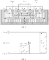
- Figure 3 is a schematic structural diagram of devices corresponding to the circuit diagram in the embodiment of Figure 2 .
- the power pad, the ground pad and the input pad are all located on a substrate (in order to more clearly describe current flow directions between the pads and the doped regions, the power pad, the ground pad and the input pad are not plotted on the substrate in Figure 3 ), and the substrate is a P-type substrate.
- the substrate is provided with a first N-type deep well 21, and the first N-type deep well 21 is provided with a first P-type well 31, a first N-type well 41 and a second P-type well 32.
- the first P-type well 31 is provided with a first P-type heavily doped region 301 and a first N-type heavily doped region 401, and the first N-type heavily doped region 401 is electrically connected to the ground pad.
- the first N-type well 41 is provided with a second P-type heavily doped region 302, a second N-type heavily doped region 402 and a third P-type heavily doped region 303, the second N-type heavily doped region 402 is electrically connected to the first P-type heavily doped region 301, and the second P-type heavily doped region 302 and the third P-type heavily doped region 303 are both electrically connected to the input pad.
- the second P-type well 32 is provided with a third N-type heavily doped region 403 and a fourth P-type heavily doped region 304, the third N-type heavily doped region 403 is electrically connected to the power pad, and the fourth P-type heavily doped region 304 is electrically connected to the second N-type heavily doped region 402.
- the first N-type well 41, the second P-type well 32 and the third N-type heavily doped region 403 jointly form the first NPN transistor Q1.
- the third P-type heavily doped region 303, the first N-type well 41 and the second P-type well 32 jointly form the first PNP transistor Q2.
- the fourth P-type heavily doped region 304 and the third N-type heavily doped region 403 jointly form the first diode D1.
- the third P-type heavily doped region 303 and the second N-type heavily doped region 402 jointly form the second diode D2.
- the resistor R1 and the resistor R2 in the first resistor unit are formed between the first N-type well 41 and the second P-type well 32.
- the first N-type well 41, the first P-type well 31 and the second N-type heavily doped region 402 jointly form the second NPN transistor Q3.
- the second P-type heavily doped region 302, the first N-type well 41 and the first P-type well 31 jointly form the second PNP transistor Q4.
- the first P-type heavily doped region 301 and the first N-type heavily doped region 401 jointly form the third diode D3.
- the second P-type heavily doped region 302 and the second N-type heavily doped region 402 jointly form the fourth diode D4.
- the resistor R3 and the resistor R4 in the second resistor unit are formed between the first N-type well 41 and the first P-type well 31.
- the small black arrow shows the current flow direction of the diode current path
- the large white arrow shows the current flow direction of the SCR current path.
- the diode current path is first turned on between the input pad and the ground pad; that is, the current flows from the input pad to the power pad along the second P-type heavily doped region 302, the second N-type heavily doped region 402, the first P-type heavily doped region 301 and the first N-type heavily doped region 401, so as to further trigger the turn-on of the SCR current path. That is, the electrostatic current is discharged through the second PNP transistor Q4 and the second NPN transistor Q3. Therefore, the electrostatic protection circuit according to this embodiment can prevent the electrostatic current from flowing through the internal circuit, thereby realizing the electrostatic protection for the internal circuit.
- Figure 4 is a circuit diagram of a protection circuit against static electricity in an ND mode according to an embodiment. As shown in Figure 4 , in this embodiment, the third circuit 13 and the fourth circuit 14 are configured to protect the internal circuit against the static electricity in the ND mode.
- the ND mode refers to an electrostatic discharge mode in which the electrostatic voltage is negative to the power supply voltage.
- the third circuit 13 includes a third NPN transistor Q5 and a third PNP transistor Q6.An emitter of the third NPN transistor Q5 is connected to the input pad, a base of the third NPN transistor Q5 is connected to a collector of the third PNP transistor Q6, a collector of the third NPN transistor Q5 and a base of the third PNP transistor Q6, an emitter of the third PNP transistor Q6 is connected to the power pad, a fifth diode D5 is connected between the base and the emitter of the third NPN transistor Q5, and a sixth diode D6 is connected between the emitter and the base of the third PNP transistor Q6.
- the fifth diode D5 and the sixth diode D6 jointly form a diode current path
- the third NPN transistor Q5 and the third PNP transistor Q6 jointly form an SCR current path.
- the fourth circuit 14 includes a fourth NPN transistor Q7 and a fourth PNP transistor Q8.An emitter of the fourth NPN transistor Q7 is connected to the ground pad, a base of the fourth NPN transistor Q7 is connected to a collector of the fourth PNP transistor Q8, a collector of the fourth NPN transistor Q7 and a base of the fourth PNP transistor Q8, an emitter of the fourth PNP transistor Q8 is connected to the power pad, a seventh diode D7 is connected between the base and the emitter of the fourth NPN transistor Q7, and an eighth diode D8 is connected between the emitter and the base of the fourth PNP transistor Q8.
- the seventh diode D7 and the eighth diode D8 jointly form a diode current path
- the fourth NPN transistor Q7 and the fourth PNP transistor Q8 jointly form an SCR current path.
- the power supply voltage is inputted to the input pad, the ground pad is connected to the ground, and the internal circuit operates normally. It may be understood that due to circuit characteristics of a diode structure and an SCR structure, an on-voltage of the diode current path is less than that of the SCR current path.
- the electrostatic voltage is negative to the power supply voltage, and in the circuit structure according to this embodiment, the diode current path in the third circuit 13 and the fourth circuit 14 is turned on first, and then, the corresponding SCR current path is triggered to be turned on through a drainage effect, and due to a positive feedback effect inside the SCR current path, the third NPN transistor Q5, the third PNP transistor Q6, the fourth NPN transistor Q7 and the fourth PNP transistor Q8 can be quickly saturated and turned on, thereby realizing a lower trigger voltage and a faster start speed than the SCR structure alone.
- the third circuit 13 and the fourth circuit 14 according to this embodiment have small parasitic capacitance, which does not affect an operating state of the internal circuit, and sustaining voltages of the third circuit 13 and the fourth circuit 14 according to this embodiment may be greater than an operating voltage, thereby avoiding a latch-up effect, that is, preventing the disorder of circuit functions or direct failure of the circuit, so as to improve the reliability and stability of the electrostatic protection circuit.
- the third circuit 13 and the fourth circuit 14 are configured to protect the internal circuit jointly against the static electricity in the ND mode.
- the SCR current path is further turned on by using the characteristics of the low trigger voltage of the diode current path and through the drainage effect of the diode current path, so as to provide a protection circuit with a low trigger voltage and a fast start speed against the static electricity in the ND mode.
- a third resistor unit is connected between the base and the collector of the third NPN transistor Q5, and a fourth resistor unit is connected between the base and the collector of the fourth NPN transistor Q7.
- the third resistor unit may include a resistor R5 and a resistor R6, and the fourth resistor unit may include a resistor R7 and a resistor R8.
- the third resistor unit and the fourth resistor unit are provided, so that the third NPN transistor Q5 and the fourth NPN transistor Q7 can be accelerated into a saturation state, so as to increase a current discharge speed of the third circuit 13.
- the fourth resistor unit may increase a current discharge speed of the fourth circuit 14. Therefore, the third circuit 13 and the fourth circuit 14 according to this embodiment further increase an ESD protection speed for the internal circuit.
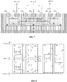
- Figure 5 is a schematic structural diagram of devices corresponding to the circuit diagram in the embodiment of Figure 4 .
- the power pad, the ground pad and the input pad are all located on a substrate (in order to more clearly describe current flow directions between the pads and the doped regions, the power pad, the ground pad and the input pad are not plotted on the substrate in Figure 5 ), and the substrate is a P-type substrate.
- the substrate is provided with a second N-type deep well 22, and the second N-type deep well 22 is provided with a third P-type well 33, a second N-type well 42 and a fourth P-type well 34.
- the third P-type well 33 is provided with a fifth P-type heavily doped region 305 and a fourth N-type heavily doped region 404, and the fourth N-type heavily doped region 404 is electrically connected to the ground pad.
- the second N-type well 42 is provided with a sixth P-type heavily doped region 306, a fifth N-type heavily doped region 405 and a seventh P-type heavily doped region 307, the fifth N-type heavily doped region 405 is electrically connected to the fifth P-type heavily doped region 305, and the sixth P-type heavily doped region 306 and the seventh P-type heavily doped region 307 are both electrically connected to the power pad.
- the fourth P-type well 34 is provided with a sixth N-type heavily doped region 406 and an eighth P-type heavily doped region 308, the sixth N-type heavily doped region 406 is electrically connected to the input pad, and the eighth P-type heavily doped region 308 is electrically connected to the fifth N-type heavily doped region 405.
- the second N-type well 42, the fourth P-type well 34 and the sixth N-type heavily doped region 406 jointly form the third NPN transistor Q5.
- the seventh P-type heavily doped region 307, the second N-type well 42 and the fourth P-type well 34 jointly form the third PNP transistor Q6.
- the eighth P-type heavily doped region 308 and the sixth N-type heavily doped region 406 jointly form the fifth diode D5.
- the seventh P-type heavily doped region 307 and the fifth N-type heavily doped region 405 jointly form the sixth diode D6.
- the resistor R5 and the resistor R6 in the third resistor unit are formed between the second N-type well 42 and the fourth P-type well 34.
- the second N-type well 42, the third P-type well 33 and the fourth N-type heavily doped region 404 jointly form the fourth NPN transistor Q7.
- the sixth P-type heavily doped region 306, the second N-type well 42 and the third P-type well 33 jointly form the fourth PNP transistor Q8.
- the fifth P-type heavily doped region 305 and the fourth N-type heavily doped region 404 jointly form the seventh diode D7.
- the sixth P-type heavily doped region 306 and the fifth N-type heavily doped region 405 jointly form the eighth diode D8.
- the resistor R7 and the resistor R8 in the fourth resistor unit are formed between the second N-type well 42 and the third P-type well 33.
- the small black arrow shows the current flow direction of the diode current path
- the large white arrow shows the current flow direction of the SCR current path.
- the diode current path is first turned on between the power pad and the ground pad; that is, the current flows from the power pad to the input pad along the sixth P-type heavily doped region 306, the fifth N-type heavily doped region 405, the fifth P-type heavily doped region 305 and the fourth N-type heavily doped region 404, so as to further trigger the turn-on of the SCR current path. That is, the electrostatic current is discharged through the eighth PNP transistor and the seventh NPN transistor. Therefore, the electrostatic protection circuit according to this embodiment can prevent the electrostatic current from flowing through the internal circuit, thereby realizing the electrostatic protection for the internal circuit.
- Figure 6 is a circuit diagram of a protection circuit against static electricity in an NS mode according to an embodiment.
- the fifth circuit 15 and the seventh circuit 16 are configured to protect the internal circuit against the static electricity in the NS mode.
- the NS mode refers to an electrostatic discharge mode in which the electrostatic voltage is negative to the power supply voltage.
- the fifth circuit 15 includes a fifth NPN transistor Q9 and a fifth PNP transistor Q10.An emitter of the fifth NPN transistor Q9 is connected to the input pad, a base of the fifth NPN transistor Q9 is connected to a collector of the fifth PNP transistor Q10, a collector of the fifth NPN transistor Q9 and a base of the fifth PNP transistor Q10, an emitter of the fifth PNP transistor Q10 is connected to the ground pad, a ninth diode D9 is connected between the base and the emitter of the fifth NPN transistor Q9, and a tenth diode D10 is connected between the emitter and the base of the fifth PNP transistor Q10.
- the ninth diode D9 and the tenth diode D10 jointly form a diode current path
- the fifth NPN transistor Q9 and the fifth PNP transistor Q10 jointly form an SCR current path.
- the sixth circuit 16 includes a sixth NPN transistor Q11 and a sixth PNP transistor Q12.An emitter of the sixth NPN transistor Q11 is connected to the power pad, a base of the sixth NPN transistor Q11 is connected to a collector of the sixth PNP transistor Q12, a collector of the sixth NPN transistor Q11 and a base of the sixth PNP transistor Q12, an emitter of the sixth PNP transistor Q12 is connected to the ground pad, an eleventh diode D11 is connected between the base and the emitter of the sixth NPN transistor Q11, and a twelfth diode D12 is connected between the emitter and the base of the sixth PNP transistor Q12.
- the eleventh diode D11 and the twelfth diode D12 jointly form a diode current path
- the sixth NPN transistor Q11 and the sixth PNP transistor Q12 jointly form an SCR current path.
- the power supply voltage is inputted to the input pad, the power pad is connected to the ground, and the internal circuit operates normally. It may be understood that due to circuit characteristics of a diode structure and an SCR structure, an on-voltage of the diode current path is less than that of the SCR current path.
- the diode current path in the fifth circuit 15 and the sixth circuit 16 may be turned on first, and then, the corresponding SCR current path is triggered to be turned on through a drainage effect, and due to a positive feedback effect inside the SCR current path, the fifth NPN transistor Q9, the fifth PNP transistor Q10, the sixth NPN transistor Q11 and the sixth PNP transistor Q12 can be quickly saturated and turned on, thereby realizing a lower trigger voltage and a faster start speed than the SCR structure alone.
- the fifth circuit 15 and the sixth circuit 16 according to this embodiment have small parasitic capacitance, which does not affect an operating state of the internal circuit, and sustaining voltages of the fifth circuit 15 and the sixth circuit 16 according to this embodiment may be greater than an operating voltage, thereby avoiding a latch-up effect, that is, preventing the disorder of circuit functions or direct failure of the circuit, so as to improve the reliability and stability of the electrostatic protection circuit.
- the fifth circuit 15 and the sixth circuit 16 are configured to protect the internal circuit jointly against the static electricity in the NS mode.
- the SCR current path is further turned on by using the characteristics of the low trigger voltage of the diode current path and through the drainage effect of the diode current path, so as to provide a protection circuit with a low trigger voltage and a fast start speed against the static electricity in the NS mode.
- a fifth resistor unit is connected between the base and the collector of the fifth NPN transistor Q9
- a sixth resistor unit is connected between the base and the collector of the sixth NPN transistor Q11.
- the fifth resistor unit may include a resistor R9 and a resistor R10
- the sixth resistor unit may include a resistor R11 and a resistor R12.
- the fifth resistor unit and the sixth resistor unit are provided, so that the fifth NPN transistor Q9 and the sixth NPN transistor Q11 can be accelerated into a saturation state, so as to increase a current discharge speed of the fifth circuit 15.
- the sixth resistor unit may increase a current discharge speed of the sixth circuit 16. Therefore, the fifth circuit 15 and the sixth circuit 16 according to this embodiment further increase an ESD protection speed for the internal circuit.
- Figure 7 is a schematic structural diagram of devices corresponding to the circuit diagram in the embodiment of Figure 6 .
- the power pad, the ground pad and the input pad are all located on a substrate (in order to more clearly describe current flow directions between the pads and the doped regions, the power pad, the ground pad and the input pad are not plotted on the substrate in Figure 7 ), and the substrate is a P-type substrate.
- the substrate is provided with a third N-type deep well 23, and the third N-type deep well 23 is provided with a fifth P-type well 35, a third N-type well 43 and a sixth P-type well 36.
- the fifth P-type well 35 is provided with a ninth P-type heavily doped region 309 and a seventh N-type heavily doped region 407, and the seventh N-type heavily doped region 407 is electrically connected to the power pad.
- the third N-type well 43 is provided with a tenth P-type heavily doped region 310, an eighth N-type heavily doped region 408 and an eleventh P-type heavily doped region 311, the eighth N-type heavily doped region 408 is electrically connected to the ninth P-type heavily doped region 309, and the tenth P-type heavily doped region 310 and the eleventh P-type heavily doped region 311 are both electrically connected to the ground pad.
- the sixth P-type well 36 is provided with a ninth N-type heavily doped region 409 and a twelfth P-type heavily doped region 312, the ninth N-type heavily doped region 409 is electrically connected to the input pad, and the twelfth P-type heavily doped region 312 is electrically connected to the eighth N-type heavily doped region 408.
- the third N-type well 43, the sixth P-type well 36 and the ninth N-type heavily doped region 409 jointly form the fifth NPN transistor Q9
- the eleventh P-type heavily doped region 311, the third N-type well 43 and the sixth P-type well 36 jointly form the fifth PNP transistor Q10.
- the twelfth P-type heavily doped region 312 and the ninth N-type heavily doped region 409 jointly form the ninth diode D9.
- the eleventh P-type heavily doped region 311 and the eighth N-type heavily doped region 408 jointly form the tenth diode D10.
- the resistor R9 and the resistor R10 in the fifth resistor unit are formed between the third N-type well 43 and the sixth P-type well 36.
- the third N-type well 43, the fifth P-type well 35 and the seventh N-type heavily doped region 407 jointly form the sixth NPN transistor Q11, and the tenth P-type heavily doped region 310, the third N-type well 43 and the fifth P-type well 35 jointly form the sixth PNP transistor Q12.
- the ninth P-type heavily doped region 309 and the seventh N-type heavily doped region 407 jointly form the eleventh diode D11.
- the tenth P-type heavily doped region 310 and the eighth N-type heavily doped region 408 jointly form the twelfth diode D12.
- the resistor R11 and the resistor R12 in the sixth resistor unit are formed between the third N-type well 43 and the fifth P-type well 35.
- the small black arrow shows the current flow direction of the diode current path
- the large white arrow shows the current flow direction of the SCR current path.
- the diode current path is first turned on between the ground pad and the power pad; that is, the current flows from the ground pad to the input pad along the tenth P-type heavily doped region 310, the eighth N-type heavily doped region 408, the ninth P-type heavily doped region 309 and the seventh N-type heavily doped region 407, so as to further trigger the turn-on of the SCR current path. That is, the electrostatic current is discharged through the sixth PNP transistor Q12 and the sixth NPN transistor Q11. Therefore, the electrostatic protection circuit according to this embodiment can prevent the electrostatic current from flowing through the internal circuit, thereby realizing the electrostatic protection for the internal circuit.
- FIG. 8 is a circuit diagram of a full-mode electrostatic protection circuit according to an embodiment.
- the electrostatic protection circuit includes a first circuit 11, a second circuit 12, a third circuit 13, a fourth circuit 14, a fifth circuit 15 and a sixth circuit 16, and each circuit includes the diode current path and the SCR current path described above.
- the first circuit 11 and the second circuit 12 jointly provide protection against static electricity in a PS mode and a PD mode
- the third circuit 13 and the fourth circuit 14 jointly provide protection against static electricity in an ND mode
- the fifth circuit 15 and the sixth circuit 16 jointly provide protection against static electricity in an NS mode, so as to realize a full-mode, all-chip electrostatic protection circuit with a low trigger voltage and a fast start speed.
- the PS mode, the PD mode, the NS mode and the ND mode are all sub-modes of a human-body model (HBM) mode, i.e., an electrostatic discharge mode in which a device is discharged by a charged human body.
- HBM human-body model
- the electrostatic protection circuit according to this embodiment may also be configured to protect against static electricity in a charged device model (CDM) mode.
- CDM mode is an electrostatic discharge mode in which a charged device directly discharges to the ground.
- the electrostatic protection circuit according to this embodiment performs protection against the static electricity in the CDM mode, so as to further improve the electrostatic protection capability and reliability of semiconductor devices.
Landscapes
- Engineering & Computer Science (AREA)
- Microelectronics & Electronic Packaging (AREA)
- Semiconductor Integrated Circuits (AREA)
- Metal-Oxide And Bipolar Metal-Oxide Semiconductor Integrated Circuits (AREA)
Abstract
Description
- This application claims priority to
Chinese Patent Application No. 202010395921.8, entitled "ELECTROSTATIC PROTECTION CIRCUIT" and filed with China Patent Office on May 12, 2020 - The present invention relates to the field of semiconductors, in particular to an electrostatic protection circuit.
- With the continuous development of semiconductor manufacturing processes, people's requirement for semiconductor devices is also constantly improving. The devices have constantly shrinking volumes, and accordingly, the semiconductor devices have increasingly shorter channels, increasingly larger junction depths, and increasingly thinner oxide layers. Therefore, the requirement for electrostatic protection capability is also constantly improving.
- A dynamic random access memory (DRAM) is a semiconductor device with a fast data access function, and mainly develops toward a faster access speed and a larger data storage quantity. However, existing electrostatic protection circuits cannot meet the requirement for electrostatic protection of a high-speed interface, which operates at a low voltage, of the DRAM and other advanced processes.
- In view of the above, the present application provides an electrostatic protection circuit.
- An electrostatic protection circuit for protecting an internal circuit, the electrostatic protection circuit including:
- a first circuit connected between a power pad and an input pad and configured to discharge a first electrostatic current, the first electrostatic current flowing from the input pad to the power pad;
- a second circuit connected between the input pad and a ground pad and configured to discharge a second electrostatic current, the second electrostatic current flowing from the input pad to the ground pad;
- a third circuit connected between the power pad and the input pad and configured to discharge a third electrostatic current, the third electrostatic current flowing from the power pad to the input pad;
- a fourth circuit connected between the power pad and the ground pad and configured to discharge a fourth electrostatic current, the fourth electrostatic current flowing from the power pad to the ground pad;
- a fifth circuit connected between the input pad and the ground pad and configured to discharge a fifth electrostatic current, the fifth electrostatic current flowing from the ground pad to the input pad; and
- a sixth circuit connected between the ground pad and the power pad and configured to discharge a sixth electrostatic current, the sixth electrostatic current flowing from the ground pad to the power pad.
- Details of one or more embodiments of the present invention are set forth in the following accompanying drawings and descriptions. Other features, objectives and advantages of the present invention become obvious with reference to the specification, the accompanying drawings and the claims.
- In order to better describe and illustrate embodiments of the present application, reference may be made to one or more accompanying drawings, while the additional details or examples for describing the accompanying drawings should not be regarded as limitations on any one of the invention creations, the embodiments described currently, and the preferred embodiments of the present application.
-
Figure 1 is a schematic structural diagram of an electrostatic protection circuit according to an embodiment; -
Figure 2 is a circuit diagram of a protection circuit against static electricity in a PS mode and a PD mode according to an embodiment; -
Figure 3 is a schematic structural diagram of devices corresponding to the circuit diagram in the embodiment ofFigure 2 ; -
Figure 4 is a circuit diagram of a protection circuit against static electricity in an ND mode according to an embodiment; -
Figure 5 is a schematic structural diagram of devices corresponding to the circuit diagram in the embodiment ofFigure 4 ; -
Figure 6 is a circuit diagram of a protection circuit against static electricity in an NS mode according to an embodiment; -
Figure 7 is a schematic structural diagram of devices corresponding to the circuit diagram in the embodiment ofFigure 6 ; and -
Figure 8 is a circuit diagram of a full-mode electrostatic protection circuit according to an embodiment. - In order to easily understand the present application, a more comprehensive description of the present application is given below with reference to the accompanying drawings. Preferred embodiments of the present application are given in the accompanying drawings. However, the present application may be implemented in many different forms and is not limited to the embodiments described herein. On the contrary, these embodiments are provided to understand the disclosed content of the present application more thoroughly and comprehensively.
- Unless otherwise defined, all technical and scientific terms used herein have the same meaning as commonly understood by those of ordinary skill in the art to which the present application belongs. The terms used in the specification of the present application are intended only to describe particular embodiments and are not intended to limit the present application.
- Spatial relationship terms such as "under", "underneath", "below", "beneath", "over", and "above" may be used for illustrative purposes to describe a relationship between one element or feature and another element or feature illustrated in the drawings. It should be understood that, in addition to the orientations illustrated in the drawings, the spatial relationship terms are intended to further include different orientations of the device in use and operation. For example, if the device in the drawings is flipped, the element or feature described as "below", "underneath" or "under" another element or feature may be oriented as "on" the another element or feature. Thus, the exemplary terms "below" and "under" may include two orientations of above and below. In addition, the device may include additional orientations (e.g., 90-degree rotation or other orientations), and thus spatial descriptors used herein may be interpreted accordingly.
- In use, the singular forms of "a", "one", and "/the" may also include plural forms, unless otherwise clearly specified by the context. It should be further understood that the terms "include/comprise" and/or "have" specify the presence of the features, integers, steps, operations, components, portions, or their combinations, but may not exclude the presence or addition of one or more of other features, integers, steps, operations, components, portions, or their combinations. At the same time, in the specification, the term "and/or" includes any and all combinations of one or more of the associated listed items.
- Embodiments of the present invention are described herein with reference to cross-sectional views of schematic diagrams of ideal embodiments (and intermediate structures) of the present invention. Correspondingly, illustrated shape variations caused by, for example, manufacturing techniques and/or tolerances, may be expected. Thus, the embodiments of the present invention should not be limited to the specific shapes of the regions illustrated herein, but may include shape deviations caused by, for example, the manufacturing techniques. For example, an implanted region illustrated as a rectangle, typically, has rounded or curved features and/or a gradient of implant concentration at its edges rather than a binary change from an implanted region to a non-implanted region. Likewise, a buried region formed by implantation may result in some implantation in the region between the buried region and a surface through which the implantation takes place. Thus, the region shown in the drawings is essentially schematic, and the illustrated shape is not intended to show the actual shape of the region of the device, and is not intended to limit the scope of the present invention.
-
Figure 1 is a schematic structural diagram of an electrostatic protection circuit according to an embodiment. The electrostatic protection circuit is configured to protect an internal circuit. As shown inFigure 1 , in this embodiment, the electrostatic protection circuit includes afirst circuit 11, asecond circuit 12, athird circuit 13, afourth circuit 14, afifth circuit 15 and asixth circuit 16. - The
first circuit 11 is connected between a power pad and an input pad and configured to discharge a first electrostatic current, the first electrostatic current flowing from the input pad to the power pad. - The
second circuit 12 is connected between the input pad and a ground pad and configured to discharge a second electrostatic current, the second electrostatic current flowing from the input pad to the ground pad. - The
third circuit 13 is connected between the power pad and the input pad and configured to discharge a third electrostatic current, the third electrostatic current flowing from the power pad to the input pad. - The
fourth circuit 14 is connected between the power pad and the ground pad and configured to discharge a fourth electrostatic current, the fourth electrostatic current flowing from the power pad to the ground pad. - The
fifth circuit 15 is connected between the input pad and the ground pad and configured to discharge a fifth electrostatic current, the fifth electrostatic current flowing from the ground pad to the input pad. - The
sixth circuit 16 is connected between the ground pad and the power pad and configured to discharge a sixth electrostatic current, the sixth electrostatic current flowing from the ground pad to the power pad. - In this embodiment, the
first circuit 11 to thesixth circuit 16 are respectively configured to discharge an electrostatic current between two pads along a set current flow direction, and when static electricity is in different electrostatic modes, discharge circuits corresponding to different electrostatic currents are turned on. Further, trigger voltages of thefirst circuit 11, thesecond circuit 12, thethird circuit 13, thefourth circuit 14, thefifth circuit 15 and thesixth circuit 16 according to this embodiment are all lower than a trigger voltage of the internal circuit. Therefore, the electrostatic protection circuit according to this embodiment can quickly discharge the electrostatic current without triggering the internal circuit, which does not affect the normal function of the internal circuit and provides relatively strong electrostatic protection capability. -
Figure 2 is a circuit diagram of a protection circuit against static electricity in a PS mode and a PD mode according to an embodiment. As shown inFigure 2 , in this embodiment, thefirst circuit 11 and thesecond circuit 12 are configured to protect the internal circuit against static electricity in the PS mode and the PD mode. The PS mode refers to an electrostatic discharge mode in which an electrostatic voltage is positive to a ground voltage, while the PD mode refers to an electrostatic discharge mode in which the electrostatic voltage is positive to a power supply voltage. - The
first circuit 11 includes a first NPN transistor Q1 and a first PNP transistor Q2.An emitter of the first NPN transistor Q1 is connected to the power pad, a base of the first NPN transistor Q1 is connected to a collector of the first PNP transistor Q2, a collector of the first NPN transistor Q1 and a base of the first PNP transistor Q2, an emitter of the first PNP transistor Q2 is connected to the input pad, a first diode D1 is connected between the base and the emitter of the first NPN transistor Q1, and a second diode D2 is connected between the emitter and the base of the first PNP transistor Q2. The first diode D1 and the second diode D2 jointly form a diode current path, and the first NPN transistor Q1 and the first PNP transistor Q2 jointly form a silicon controlled rectifier (SCR) current path. - The
second circuit 12 includes a second NPN transistor Q3 and a second PNP transistor Q4.An emitter of the second NPN transistor Q3 is connected to the ground pad, a base of the second NPN transistor Q3 is connected to a collector of the second PNP transistor Q4, a collector of the second NPN transistor Q3 and a base of the second PNP transistor Q4, an emitter of the second PNP transistor Q4 is connected to the input pad, a third diode D3 is connected between the base and the emitter of the second NPN transistor Q3, and a fourth diode D4 is connected between the emitter and the base of the second PNP transistor Q4. The third diode D3 and the fourth diode D4 jointly form a diode current path, and the second NPN transistor Q3 and the second PNP transistor Q4 jointly form an SCR current path. - Specifically, when no electro-static discharge (ESD) happens, the power supply voltage is inputted to the power pad, the ground pad is connected to the ground, and the internal circuit operates normally. It may be understood that due to circuit characteristics of a diode structure and an SCR structure, an on-voltage of the diode current path is less than that of the SCR current path. Therefore, when ESD in the PS mode and the PD mode happens, the electrostatic voltage is positive to the power supply voltage or to the ground voltage, and in the circuit structure according to this embodiment, the diode current path in the
first circuit 11 and thesecond circuit 12 is turned on first, and then, the corresponding SCR current path is triggered to be turned on through a drainage effect, and due to a positive feedback effect inside the SCR current path, the first NPN transistor Q1, the first PNP transistor Q2, the second NPN transistor Q3 and the second PNP transistor Q4 can be quickly saturated and turned on, thereby realizing a lower trigger voltage and a faster start speed than the SCR structure alone. - Further, the
first circuit 11 and thesecond circuit 12 according to this embodiment have small parasitic capacitance, which does not affect an operating state of the internal circuit, and sustaining voltages of thefirst circuit 11 and thesecond circuit 12 according to this embodiment may be greater than an operating voltage, thereby avoiding a latch-up effect, that is, preventing the disorder of circuit functions or direct failure of the circuit, so as to improve the reliability and stability of the electrostatic protection circuit. - In this embodiment, the
first circuit 11 and thesecond circuit 12 are configured to protect the internal circuit jointly against the static electricity in the PS mode and the PD mode. Through the diode current path and the SCR current path arranged inside thefirst circuit 11, the SCR current path is further turned on by using the characteristics of the low trigger voltage of the diode current path and through the drainage effect of the diode current path, so as to provide a protection circuit with a low trigger voltage and a fast start speed against the static electricity in the PS mode and the PD mode. - Still referring to
Figure 2 , a first resistor unit is connected between the base and the collector of the first NPN transistor Q1, and a second resistor unit is connected between the base and the collector of the second NPN transistor Q3. Specifically, the first resistor unit may include a resistor R1 and a resistor R2, and the second resistor unit may include a resistor R3 and a resistor R4. In this embodiment, the first resistor unit and the second resistor unit are provided, so that the first NPN transistor Q1 and the second NPN transistor Q3 can be accelerated into a saturation state, so as to increase a current discharge speed of thefirst circuit 11. Similarly, the second resistor unit may increase a current discharge speed of thesecond circuit 12. Therefore, thefirst circuit 11 and thesecond circuit 12 according to this embodiment further increase an ESD protection speed for the internal circuit. -
Figure 3 is a schematic structural diagram of devices corresponding to the circuit diagram in the embodiment ofFigure 2 . In this embodiment, the power pad, the ground pad and the input pad are all located on a substrate (in order to more clearly describe current flow directions between the pads and the doped regions, the power pad, the ground pad and the input pad are not plotted on the substrate inFigure 3 ), and the substrate is a P-type substrate. - As shown in
Figure 3 , the substrate is provided with a first N-type deep well 21, and the first N-type deep well 21 is provided with a first P-type well 31, a first N-type well 41 and a second P-type well 32. The first P-type well 31 is provided with a first P-type heavily dopedregion 301 and a first N-type heavily dopedregion 401, and the first N-type heavily dopedregion 401 is electrically connected to the ground pad. The first N-type well 41 is provided with a second P-type heavily dopedregion 302, a second N-type heavily dopedregion 402 and a third P-type heavily dopedregion 303, the second N-type heavily dopedregion 402 is electrically connected to the first P-type heavily dopedregion 301, and the second P-type heavily dopedregion 302 and the third P-type heavily dopedregion 303 are both electrically connected to the input pad. The second P-type well 32 is provided with a third N-type heavily dopedregion 403 and a fourth P-type heavily dopedregion 304, the third N-type heavily dopedregion 403 is electrically connected to the power pad, and the fourth P-type heavily dopedregion 304 is electrically connected to the second N-type heavily dopedregion 402. - Specifically, the first N-
type well 41, the second P-type well 32 and the third N-type heavily dopedregion 403 jointly form the first NPN transistor Q1. The third P-type heavily dopedregion 303, the first N-type well 41 and the second P-type well 32 jointly form the first PNP transistor Q2. The fourth P-type heavily dopedregion 304 and the third N-type heavily dopedregion 403 jointly form the first diode D1. The third P-type heavily dopedregion 303 and the second N-type heavily dopedregion 402 jointly form the second diode D2. The resistor R1 and the resistor R2 in the first resistor unit are formed between the first N-type well 41 and the second P-type well 32. The first N-type well 41, the first P-type well 31 and the second N-type heavily dopedregion 402 jointly form the second NPN transistor Q3. The second P-type heavily dopedregion 302, the first N-type well 41 and the first P-type well 31 jointly form the second PNP transistor Q4. The first P-type heavily dopedregion 301 and the first N-type heavily dopedregion 401 jointly form the third diode D3. The second P-type heavily dopedregion 302 and the second N-type heavily dopedregion 402 jointly form the fourth diode D4. The resistor R3 and the resistor R4 in the second resistor unit are formed between the first N-type well 41 and the first P-type well 31. - Further, in
Figure 3 , the small black arrow shows the current flow direction of the diode current path, and the large white arrow shows the current flow direction of the SCR current path. When the static electricity in the PS mode or the PD mode is applied, the diode current path is first turned on between the input pad and the power pad; that is, the current flows from the input pad to the power pad along the third P-type heavily dopedregion 303, the second N-type heavily dopedregion 402, the fourth P-type heavily dopedregion 304 and the third N-type heavily dopedregion 403, so as to further trigger the turn-on of the SCR current path. That is, the electrostatic current is discharged through the first PNP transistor Q2 and the first NPN transistor Q1. Similarly, the diode current path is first turned on between the input pad and the ground pad; that is, the current flows from the input pad to the power pad along the second P-type heavily dopedregion 302, the second N-type heavily dopedregion 402, the first P-type heavily dopedregion 301 and the first N-type heavily dopedregion 401, so as to further trigger the turn-on of the SCR current path. That is, the electrostatic current is discharged through the second PNP transistor Q4 and the second NPN transistor Q3. Therefore, the electrostatic protection circuit according to this embodiment can prevent the electrostatic current from flowing through the internal circuit, thereby realizing the electrostatic protection for the internal circuit. -
Figure 4 is a circuit diagram of a protection circuit against static electricity in an ND mode according to an embodiment. As shown inFigure 4 , in this embodiment, thethird circuit 13 and thefourth circuit 14 are configured to protect the internal circuit against the static electricity in the ND mode. The ND mode refers to an electrostatic discharge mode in which the electrostatic voltage is negative to the power supply voltage. - The
third circuit 13 includes a third NPN transistor Q5 and a third PNP transistor Q6.An emitter of the third NPN transistor Q5 is connected to the input pad, a base of the third NPN transistor Q5 is connected to a collector of the third PNP transistor Q6, a collector of the third NPN transistor Q5 and a base of the third PNP transistor Q6, an emitter of the third PNP transistor Q6 is connected to the power pad, a fifth diode D5 is connected between the base and the emitter of the third NPN transistor Q5, and a sixth diode D6 is connected between the emitter and the base of the third PNP transistor Q6. The fifth diode D5 and the sixth diode D6 jointly form a diode current path, and the third NPN transistor Q5 and the third PNP transistor Q6 jointly form an SCR current path. - The
fourth circuit 14 includes a fourth NPN transistor Q7 and a fourth PNP transistor Q8.An emitter of the fourth NPN transistor Q7 is connected to the ground pad, a base of the fourth NPN transistor Q7 is connected to a collector of the fourth PNP transistor Q8, a collector of the fourth NPN transistor Q7 and a base of the fourth PNP transistor Q8, an emitter of the fourth PNP transistor Q8 is connected to the power pad, a seventh diode D7 is connected between the base and the emitter of the fourth NPN transistor Q7, and an eighth diode D8 is connected between the emitter and the base of the fourth PNP transistor Q8. The seventh diode D7 and the eighth diode D8 jointly form a diode current path, and the fourth NPN transistor Q7 and the fourth PNP transistor Q8 jointly form an SCR current path. - Specifically, when no ESD happens, the power supply voltage is inputted to the input pad, the ground pad is connected to the ground, and the internal circuit operates normally. It may be understood that due to circuit characteristics of a diode structure and an SCR structure, an on-voltage of the diode current path is less than that of the SCR current path. Therefore, when ESD in the ND mode happens, the electrostatic voltage is negative to the power supply voltage, and in the circuit structure according to this embodiment, the diode current path in the
third circuit 13 and thefourth circuit 14 is turned on first, and then, the corresponding SCR current path is triggered to be turned on through a drainage effect, and due to a positive feedback effect inside the SCR current path, the third NPN transistor Q5, the third PNP transistor Q6, the fourth NPN transistor Q7 and the fourth PNP transistor Q8 can be quickly saturated and turned on, thereby realizing a lower trigger voltage and a faster start speed than the SCR structure alone. - Further, the
third circuit 13 and thefourth circuit 14 according to this embodiment have small parasitic capacitance, which does not affect an operating state of the internal circuit, and sustaining voltages of thethird circuit 13 and thefourth circuit 14 according to this embodiment may be greater than an operating voltage, thereby avoiding a latch-up effect, that is, preventing the disorder of circuit functions or direct failure of the circuit, so as to improve the reliability and stability of the electrostatic protection circuit. - In this embodiment, the
third circuit 13 and thefourth circuit 14 are configured to protect the internal circuit jointly against the static electricity in the ND mode. Through the diode current path and the SCR current path arranged inside thethird circuit 13, the SCR current path is further turned on by using the characteristics of the low trigger voltage of the diode current path and through the drainage effect of the diode current path, so as to provide a protection circuit with a low trigger voltage and a fast start speed against the static electricity in the ND mode. - Still referring to
Figure 4 , a third resistor unit is connected between the base and the collector of the third NPN transistor Q5, and a fourth resistor unit is connected between the base and the collector of the fourth NPN transistor Q7. Specifically, the third resistor unit may include a resistor R5 and a resistor R6, and the fourth resistor unit may include a resistor R7 and a resistor R8. In this embodiment, the third resistor unit and the fourth resistor unit are provided, so that the third NPN transistor Q5 and the fourth NPN transistor Q7 can be accelerated into a saturation state, so as to increase a current discharge speed of thethird circuit 13. Similarly, the fourth resistor unit may increase a current discharge speed of thefourth circuit 14. Therefore, thethird circuit 13 and thefourth circuit 14 according to this embodiment further increase an ESD protection speed for the internal circuit. -
Figure 5 is a schematic structural diagram of devices corresponding to the circuit diagram in the embodiment ofFigure 4 . In this embodiment, the power pad, the ground pad and the input pad are all located on a substrate (in order to more clearly describe current flow directions between the pads and the doped regions, the power pad, the ground pad and the input pad are not plotted on the substrate inFigure 5 ), and the substrate is a P-type substrate. As shown inFigure 5 , the substrate is provided with a second N-type deep well 22, and the second N-type deep well 22 is provided with a third P-type well 33, a second N-type well 42 and a fourth P-type well 34. The third P-type well 33 is provided with a fifth P-type heavily dopedregion 305 and a fourth N-type heavily dopedregion 404, and the fourth N-type heavily dopedregion 404 is electrically connected to the ground pad. The second N-type well 42 is provided with a sixth P-type heavily dopedregion 306, a fifth N-type heavily dopedregion 405 and a seventh P-type heavily dopedregion 307, the fifth N-type heavily dopedregion 405 is electrically connected to the fifth P-type heavily dopedregion 305, and the sixth P-type heavily dopedregion 306 and the seventh P-type heavily dopedregion 307 are both electrically connected to the power pad. The fourth P-type well 34 is provided with a sixth N-type heavily dopedregion 406 and an eighth P-type heavily dopedregion 308, the sixth N-type heavily dopedregion 406 is electrically connected to the input pad, and the eighth P-type heavily dopedregion 308 is electrically connected to the fifth N-type heavily dopedregion 405. - Specifically, the second N-
type well 42, the fourth P-type well 34 and the sixth N-type heavily dopedregion 406 jointly form the third NPN transistor Q5. The seventh P-type heavily dopedregion 307, the second N-type well 42 and the fourth P-type well 34 jointly form the third PNP transistor Q6. The eighth P-type heavily dopedregion 308 and the sixth N-type heavily dopedregion 406 jointly form the fifth diode D5. The seventh P-type heavily dopedregion 307 and the fifth N-type heavily dopedregion 405 jointly form the sixth diode D6. The resistor R5 and the resistor R6 in the third resistor unit are formed between the second N-type well 42 and the fourth P-type well 34. The second N-type well 42, the third P-type well 33 and the fourth N-type heavily dopedregion 404 jointly form the fourth NPN transistor Q7. The sixth P-type heavily dopedregion 306, the second N-type well 42 and the third P-type well 33 jointly form the fourth PNP transistor Q8. The fifth P-type heavily dopedregion 305 and the fourth N-type heavily dopedregion 404 jointly form the seventh diode D7. The sixth P-type heavily dopedregion 306 and the fifth N-type heavily dopedregion 405 jointly form the eighth diode D8. The resistor R7 and the resistor R8 in the fourth resistor unit are formed between the second N-type well 42 and the third P-type well 33. - Further, in
Figure 5 , the small black arrow shows the current flow direction of the diode current path, and the large white arrow shows the current flow direction of the SCR current path. When the static electricity in the ND mode is applied, the diode current path is first turned on between the power pad and the input pad; that is, the current flows from the power pad to the input pad along the seventh P-type heavily dopedregion 307, the fifth N-type heavily dopedregion 405, the eighth P-type heavily dopedregion 308 and the sixth N-type heavily dopedregion 406, so as to further trigger the turn-on of the SCR current path. That is, the electrostatic current is discharged through the third PNP transistor Q6 and the third NPN transistor Q5. Similarly, the diode current path is first turned on between the power pad and the ground pad; that is, the current flows from the power pad to the input pad along the sixth P-type heavily dopedregion 306, the fifth N-type heavily dopedregion 405, the fifth P-type heavily dopedregion 305 and the fourth N-type heavily dopedregion 404, so as to further trigger the turn-on of the SCR current path. That is, the electrostatic current is discharged through the eighth PNP transistor and the seventh NPN transistor. Therefore, the electrostatic protection circuit according to this embodiment can prevent the electrostatic current from flowing through the internal circuit, thereby realizing the electrostatic protection for the internal circuit. -
Figure 6 is a circuit diagram of a protection circuit against static electricity in an NS mode according to an embodiment. As shown inFigure 6 , in this embodiment, thefifth circuit 15 and theseventh circuit 16 are configured to protect the internal circuit against the static electricity in the NS mode. The NS mode refers to an electrostatic discharge mode in which the electrostatic voltage is negative to the power supply voltage. - The
fifth circuit 15 includes a fifth NPN transistor Q9 and a fifth PNP transistor Q10.An emitter of the fifth NPN transistor Q9 is connected to the input pad, a base of the fifth NPN transistor Q9 is connected to a collector of the fifth PNP transistor Q10, a collector of the fifth NPN transistor Q9 and a base of the fifth PNP transistor Q10, an emitter of the fifth PNP transistor Q10 is connected to the ground pad, a ninth diode D9 is connected between the base and the emitter of the fifth NPN transistor Q9, and a tenth diode D10 is connected between the emitter and the base of the fifth PNP transistor Q10. The ninth diode D9 and the tenth diode D10 jointly form a diode current path, and the fifth NPN transistor Q9 and the fifth PNP transistor Q10 jointly form an SCR current path. - The
sixth circuit 16 includes a sixth NPN transistor Q11 and a sixth PNP transistor Q12.An emitter of the sixth NPN transistor Q11 is connected to the power pad, a base of the sixth NPN transistor Q11 is connected to a collector of the sixth PNP transistor Q12, a collector of the sixth NPN transistor Q11 and a base of the sixth PNP transistor Q12, an emitter of the sixth PNP transistor Q12 is connected to the ground pad, an eleventh diode D11 is connected between the base and the emitter of the sixth NPN transistor Q11, and a twelfth diode D12 is connected between the emitter and the base of the sixth PNP transistor Q12. The eleventh diode D11 and the twelfth diode D12 jointly form a diode current path, and the sixth NPN transistor Q11 and the sixth PNP transistor Q12 jointly form an SCR current path. - Specifically, when no ESD happens, the power supply voltage is inputted to the input pad, the power pad is connected to the ground, and the internal circuit operates normally. It may be understood that due to circuit characteristics of a diode structure and an SCR structure, an on-voltage of the diode current path is less than that of the SCR current path. Therefore, when ESD in the NS mode happens, the electrostatic voltage is negative to the ground voltage, and in the circuit structure according to this embodiment, the diode current path in the
fifth circuit 15 and thesixth circuit 16 may be turned on first, and then, the corresponding SCR current path is triggered to be turned on through a drainage effect, and due to a positive feedback effect inside the SCR current path, the fifth NPN transistor Q9, the fifth PNP transistor Q10, the sixth NPN transistor Q11 and the sixth PNP transistor Q12 can be quickly saturated and turned on, thereby realizing a lower trigger voltage and a faster start speed than the SCR structure alone. - Further, the
fifth circuit 15 and thesixth circuit 16 according to this embodiment have small parasitic capacitance, which does not affect an operating state of the internal circuit, and sustaining voltages of thefifth circuit 15 and thesixth circuit 16 according to this embodiment may be greater than an operating voltage, thereby avoiding a latch-up effect, that is, preventing the disorder of circuit functions or direct failure of the circuit, so as to improve the reliability and stability of the electrostatic protection circuit. - In this embodiment, the
fifth circuit 15 and thesixth circuit 16 are configured to protect the internal circuit jointly against the static electricity in the NS mode. - Through the diode current path and the SCR current path arranged inside the
fifth circuit 15, the SCR current path is further turned on by using the characteristics of the low trigger voltage of the diode current path and through the drainage effect of the diode current path, so as to provide a protection circuit with a low trigger voltage and a fast start speed against the static electricity in the NS mode. - Still referring to
Figure 6 , a fifth resistor unit is connected between the base and the collector of the fifth NPN transistor Q9, and a sixth resistor unit is connected between the base and the collector of the sixth NPN transistor Q11. Specifically, the fifth resistor unit may include a resistor R9 and a resistor R10, and the sixth resistor unit may include a resistor R11 and a resistor R12. In this embodiment, the fifth resistor unit and the sixth resistor unit are provided, so that the fifth NPN transistor Q9 and the sixth NPN transistor Q11 can be accelerated into a saturation state, so as to increase a current discharge speed of thefifth circuit 15. Similarly, the sixth resistor unit may increase a current discharge speed of thesixth circuit 16. Therefore, thefifth circuit 15 and thesixth circuit 16 according to this embodiment further increase an ESD protection speed for the internal circuit. -
Figure 7 is a schematic structural diagram of devices corresponding to the circuit diagram in the embodiment ofFigure 6 . In this embodiment, the power pad, the ground pad and the input pad are all located on a substrate (in order to more clearly describe current flow directions between the pads and the doped regions, the power pad, the ground pad and the input pad are not plotted on the substrate inFigure 7 ), and the substrate is a P-type substrate. As shown inFigure 7 , the substrate is provided with a third N-type deep well 23, and the third N-type deep well 23 is provided with a fifth P-type well 35, a third N-type well 43 and a sixth P-type well 36. The fifth P-type well 35 is provided with a ninth P-type heavily dopedregion 309 and a seventh N-type heavily dopedregion 407, and the seventh N-type heavily dopedregion 407 is electrically connected to the power pad. The third N-type well 43 is provided with a tenth P-type heavily dopedregion 310, an eighth N-type heavily dopedregion 408 and an eleventh P-type heavily dopedregion 311, the eighth N-type heavily dopedregion 408 is electrically connected to the ninth P-type heavily dopedregion 309, and the tenth P-type heavily dopedregion 310 and the eleventh P-type heavily dopedregion 311 are both electrically connected to the ground pad. The sixth P-type well 36 is provided with a ninth N-type heavily dopedregion 409 and a twelfth P-type heavily dopedregion 312, the ninth N-type heavily dopedregion 409 is electrically connected to the input pad, and the twelfth P-type heavily dopedregion 312 is electrically connected to the eighth N-type heavily dopedregion 408. - Specifically, the third N-
type well 43, the sixth P-type well 36 and the ninth N-type heavily dopedregion 409 jointly form the fifth NPN transistor Q9, and the eleventh P-type heavily dopedregion 311, the third N-type well 43 and the sixth P-type well 36 jointly form the fifth PNP transistor Q10. The twelfth P-type heavily dopedregion 312 and the ninth N-type heavily dopedregion 409 jointly form the ninth diode D9. The eleventh P-type heavily dopedregion 311 and the eighth N-type heavily dopedregion 408 jointly form the tenth diode D10. The resistor R9 and the resistor R10 in the fifth resistor unit are formed between the third N-type well 43 and the sixth P-type well 36. The third N-type well 43, the fifth P-type well 35 and the seventh N-type heavily dopedregion 407 jointly form the sixth NPN transistor Q11, and the tenth P-type heavily dopedregion 310, the third N-type well 43 and the fifth P-type well 35 jointly form the sixth PNP transistor Q12. The ninth P-type heavily dopedregion 309 and the seventh N-type heavily dopedregion 407 jointly form the eleventh diode D11. The tenth P-type heavily dopedregion 310 and the eighth N-type heavily dopedregion 408 jointly form the twelfth diode D12. The resistor R11 and the resistor R12 in the sixth resistor unit are formed between the third N-type well 43 and the fifth P-type well 35. - Further, in
Figure 7 , the small black arrow shows the current flow direction of the diode current path, and the large white arrow shows the current flow direction of the SCR current path. When the static electricity in the NS mode is applied, the diode current path is first turned on between the ground pad and the input pad; that is, the current flows from the ground pad to the input pad along the eleventh P-type heavily dopedregion 311, the eighth N-type heavily dopedregion 408, the twelfth P-type heavily dopedregion 312 and the ninth N-type heavily dopedregion 409, so as to further trigger the turn-on of the SCR current path. That is, the electrostatic current is discharged through the fifth PNP transistor Q10 and the fifth NPN transistor Q9. Similarly, the diode current path is first turned on between the ground pad and the power pad; that is, the current flows from the ground pad to the input pad along the tenth P-type heavily dopedregion 310, the eighth N-type heavily dopedregion 408, the ninth P-type heavily dopedregion 309 and the seventh N-type heavily dopedregion 407, so as to further trigger the turn-on of the SCR current path. That is, the electrostatic current is discharged through the sixth PNP transistor Q12 and the sixth NPN transistor Q11. Therefore, the electrostatic protection circuit according to this embodiment can prevent the electrostatic current from flowing through the internal circuit, thereby realizing the electrostatic protection for the internal circuit. -
Figure 8 is a circuit diagram of a full-mode electrostatic protection circuit according to an embodiment. As shown inFigure 8 , in this embodiment, the electrostatic protection circuit includes afirst circuit 11, asecond circuit 12, athird circuit 13, afourth circuit 14, afifth circuit 15 and asixth circuit 16, and each circuit includes the diode current path and the SCR current path described above. Thefirst circuit 11 and thesecond circuit 12 jointly provide protection against static electricity in a PS mode and a PD mode, thethird circuit 13 and thefourth circuit 14 jointly provide protection against static electricity in an ND mode, and thefifth circuit 15 and thesixth circuit 16 jointly provide protection against static electricity in an NS mode, so as to realize a full-mode, all-chip electrostatic protection circuit with a low trigger voltage and a fast start speed. - Further, the PS mode, the PD mode, the NS mode and the ND mode are all sub-modes of a human-body model (HBM) mode, i.e., an electrostatic discharge mode in which a device is discharged by a charged human body. In addition to the HBM mode, the electrostatic protection circuit according to this embodiment may also be configured to protect against static electricity in a charged device model (CDM) mode. The CDM mode is an electrostatic discharge mode in which a charged device directly discharges to the ground. The electrostatic protection circuit according to this embodiment performs protection against the static electricity in the CDM mode, so as to further improve the electrostatic protection capability and reliability of semiconductor devices.
- In the description of the specification, reference terms such as "some embodiments", "other embodiments", and "ideal examples" mean that a particular feature, structure, material, or characteristic described in connection with the embodiment or example is included in at least one embodiment or example of the present invention. In the specification, the schematic expressions to the above terms are not necessarily referring to the same embodiment or example.
- Technical features of the above embodiments may be combined randomly. To make descriptions brief, not all possible combinations of the technical features in the embodiments are described. However, as long as there is no contradiction between the combinations of the technical features, they should all be considered as scopes disclosed in the specification.
- The above embodiments only describe several implementations of the present application, and their description is specific and detailed, but cannot therefore be understood as a limitation on the patent scope of the present application. It should be noted that those of ordinary skill in the art may further make variations and improvements without departing from the conception of the present application, and these all fall within the protection scope of the present application. Therefore, the patent protection scope of the present application should be subject to the appended claims.
Claims (10)
- An electrostatic protection circuit for protecting an internal circuit, the electrostatic protection circuit comprising:a first circuit connected between a power pad and an input pad and configured to discharge a first electrostatic current, the first electrostatic current flowing from the input pad to the power pad;a second circuit connected between the input pad and a ground pad and configured to discharge a second electrostatic current, the second electrostatic current flowing from the input pad to the ground pad;a third circuit connected between the power pad and the input pad and configured to discharge a third electrostatic current, the third electrostatic current flowing from the power pad to the input pad;a fourth circuit connected between the power pad and the ground pad and configured to discharge a fourth electrostatic current, the fourth electrostatic current flowing from the power pad to the ground pad;a fifth circuit connected between the input pad and the ground pad and configured to discharge a fifth electrostatic current, the fifth electrostatic current flowing from the ground pad to the input pad; anda sixth circuit connected between the ground pad and the power pad and configured to discharge a sixth electrostatic current, the sixth electrostatic current flowing from the ground pad to the power pad.
- The electrostatic protection circuit according to claim 1, wherein the first circuit comprises a first NPN transistor and a first PNP transistor, an emitter of the first NPN transistor is connected to the power pad, a base of the first NPN transistor is connected to a collector of the first PNP transistor, a collector of the first NPN transistor and a base of the first PNP transistor, an emitter of the first PNP transistor is connected to the input pad, a first diode is connected between the base and the emitter of the first NPN transistor, and a second diode is connected between the emitter and the base of the first PNP transistor; and
the second circuit comprises a second NPN transistor and a second PNP transistor, an emitter of the second NPN transistor is connected to the ground pad, a base of the second NPN transistor is connected to a collector of the second PNP transistor, a collector of the second NPN transistor and a base of the second PNP transistor, an emitter of the second PNP transistor is connected to the input pad, a third diode is connected between the base and the emitter of the second NPN transistor, and a fourth diode is connected between the emitter and the base of the second PNP transistor. - The electrostatic protection circuit according to claim 2, wherein a first resistor unit is connected between the base and the collector of the first NPN transistor, and a second resistor unit is connected between the base and the collector of the second NPN transistor.
- The electrostatic protection circuit according to claim 3, wherein the ground pad and the power pad are both located on a substrate, the substrate being a P-type substrate, the substrate being provided with a first N-type deep well, and the first N-type deep well being provided with a first P-type well, a first N-type well and a second P-type well, whereinthe first P-type well is provided with a first P-type heavily doped region and a first N-type heavily doped region, the first N-type heavily doped region being electrically connected to the ground pad;the first N-type well is provided with a second P-type heavily doped region, a second N-type heavily doped region and a third P-type heavily doped region, the second N-type heavily doped region being electrically connected to the first P-type heavily doped region, and the second P-type heavily doped region and the third P-type heavily doped region being both electrically connected to the input pad; andthe second P-type well is provided with a third N-type heavily doped region and a fourth P-type heavily doped region, the third N-type heavily doped region being electrically connected to the power pad, and the fourth P-type heavily doped region being electrically connected to the second N-type heavily doped region.
- The electrostatic protection circuit according to claim 1, wherein the third circuit comprises a third NPN transistor and a third PNP transistor, an emitter of the third NPN transistor is connected to the input pad, a base of the third NPN transistor is connected to a collector of the third PNP transistor, a collector of the third NPN transistor and a base of the third PNP transistor, an emitter of the third PNP transistor is connected to the power pad, a fifth diode is connected between the base and the emitter of the third NPN transistor, and a sixth diode is connected between the emitter and the base of the third PNP transistor; and
the fourth circuit comprises a fourth NPN transistor and a fourth PNP transistor, an emitter of the fourth NPN transistor is connected to the ground pad, a base of the fourth NPN transistor is connected to a collector of the fourth PNP transistor, a collector of the fourth NPN transistor and a base of the fourth PNP transistor, an emitter of the fourth PNP transistor is connected to the power pad, a seventh diode is connected between the base and the emitter of the fourth NPN transistor, and an eighth diode is connected between the emitter and the base of the fourth PNP transistor. - The electrostatic protection circuit according to claim 5, wherein a third resistor unit is connected between the base and the collector of the third NPN transistor, and a fourth resistor unit is connected between the base and the collector of the fourth NPN transistor.
- The electrostatic protection circuit according to claim 6, wherein the ground pad and the input pad are both located on a substrate, the substrate being a P-type substrate, the substrate being provided with a second N-type deep well, and the second N-type deep well being provided with a third P-type well, a second N-type well and a fourth P-type well, whereinthe third P-type well is provided with a fifth P-type heavily doped region and a fourth N-type heavily doped region, the fourth N-type heavily doped region being electrically connected to the ground pad;the second N-type well is provided with a sixth P-type heavily doped region, a fifth N-type heavily doped region and a seventh P-type heavily doped region, the fifth N-type heavily doped region being electrically connected to the fifth P-type heavily doped region, and the sixth P-type heavily doped region and the seventh P-type heavily doped region being both electrically connected to the power pad; andthe fourth P-type well is provided with a sixth N-type heavily doped region and an eighth P-type heavily doped region, the sixth N-type heavily doped region being electrically connected to the input pad, and the eighth P-type heavily doped region being electrically connected to the fifth N-type heavily doped region.
- The electrostatic protection circuit according to claim 1, wherein the fifth circuit comprises a fifth NPN transistor and a fifth PNP transistor, an emitter of the fifth NPN transistor is connected to the input pad, a base of the fifth NPN transistor is connected to a collector of the fifth PNP transistor, a collector of the fifth NPN transistor and a base of the fifth PNP transistor, an emitter of the fifth PNP transistor is connected to the ground pad, a ninth diode is connected between the base and the emitter of the fifth NPN transistor, and a tenth diode is connected between the emitter and the base of the fifth PNP transistor; and
the sixth circuit comprises a sixth NPN transistor and a sixth PNP transistor, an emitter of the sixth NPN transistor is connected to the power pad, a base of the sixth NPN transistor is connected to a collector of the sixth PNP transistor, a collector of the sixth NPN transistor and a base of the sixth PNP transistor, an emitter of the sixth PNP transistor is connected to the ground pad, an eleventh diode is connected between the base and the emitter of the sixth NPN transistor, and a twelfth diode is connected between the emitter and the base of the sixth PNP transistor. - The electrostatic protection circuit according to claim 8, wherein a fifth resistor unit is connected between the base and the collector of the fifth NPN transistor, and a sixth resistor unit is connected between the base and the collector of the sixth NPN transistor.
- The electrostatic protection circuit according to claim 9, wherein the power pad and the input pad are both located on a substrate, the substrate being a P-type substrate, the substrate being provided with a third N-type deep well, and the third N-type deep well being provided with a fifth P-type well, a third N-type well and a sixth P-type well, whereinthe fifth P-type well is provided with a ninth P-type heavily doped region and a seventh N-type heavily doped region, the seventh N-type heavily doped region being electrically connected to the power pad;the third N-type well is provided with a tenth P-type heavily doped region, an eighth N-type heavily doped region and an eleventh P-type heavily doped region, the eighth N-type heavily doped region being electrically connected to the ninth P-type heavily doped region, and the tenth P-type heavily doped region and the eleventh P-type heavily doped region being both electrically connected to the ground pad; andthe sixth P-type well is provided with a ninth N-type heavily doped region and a twelfth P-type heavily doped region, the ninth N-type heavily doped region being electrically connected to the input pad, and the twelfth P-type heavily doped region being electrically connected to the eighth N-type heavily doped region.
Applications Claiming Priority (2)
| Application Number | Priority Date | Filing Date | Title |
|---|---|---|---|
| CN202010395921.8A CN113658945B (en) | 2020-05-12 | 2020-05-12 | Static electricity protection circuit |
| PCT/CN2021/076340 WO2021227584A1 (en) | 2020-05-12 | 2021-02-09 | Electrostatic protection circuit |
Publications (3)
| Publication Number | Publication Date |
|---|---|
| EP4020551A1 true EP4020551A1 (en) | 2022-06-29 |
| EP4020551A4 EP4020551A4 (en) | 2022-12-28 |
| EP4020551B1 EP4020551B1 (en) | 2025-07-23 |
Family
ID=78511964
Family Applications (1)
| Application Number | Title | Priority Date | Filing Date |
|---|---|---|---|
| EP21803441.1A Active EP4020551B1 (en) | 2020-05-12 | 2021-02-09 | Electrostatic protection circuit |
Country Status (2)
| Country | Link |
|---|---|
| US (1) | US11791625B2 (en) |
| EP (1) | EP4020551B1 (en) |
Families Citing this family (9)
| Publication number | Priority date | Publication date | Assignee | Title |
|---|---|---|---|---|
| CN113540070B (en) * | 2020-04-20 | 2023-12-12 | 长鑫存储技术有限公司 | Static electricity protection circuit |
| US12081018B2 (en) * | 2021-07-09 | 2024-09-03 | Changxin Memory Technologies, Inc. | Electrostatic discharge protection network for chip |
| US20230206987A1 (en) * | 2021-12-29 | 2023-06-29 | Changxin Memory Technologies, Inc. | Integrated circuit structure, memory, and integrated circuit layout |
| US11936179B2 (en) | 2022-03-11 | 2024-03-19 | Changxin Memory Technologies, Inc. | Electrostatic discharge protection circuit |
| US20240055507A1 (en) * | 2022-08-12 | 2024-02-15 | Macronix International Co., Ltd. | Electrostatic discharge protection circuit |
| KR20240108723A (en) * | 2023-01-02 | 2024-07-09 | 삼성전자주식회사 | Device for electrostatic discharge protection using silicon controlled rectifier |
| US20240348046A1 (en) * | 2023-04-11 | 2024-10-17 | Semiconductor Components Industries, Llc | Distributed electrostatic discharge protection for semiconductor device |
| KR20240177116A (en) * | 2023-06-19 | 2024-12-27 | 삼성전자주식회사 | Semiconductor device |
| CN118380462B (en) * | 2024-06-27 | 2024-09-06 | 杭州积海半导体有限公司 | Silicon controlled rectifier structure |
Family Cites Families (24)
| Publication number | Priority date | Publication date | Assignee | Title |
|---|---|---|---|---|
| US4484244A (en) * | 1982-09-22 | 1984-11-20 | Rca Corporation | Protection circuit for integrated circuit devices |
| US5359211A (en) * | 1991-07-18 | 1994-10-25 | Harris Corporation | High voltage protection using SCRs |
| US5182220A (en) * | 1992-04-02 | 1993-01-26 | United Microelectronics Corporation | CMOS on-chip ESD protection circuit and semiconductor structure |
| US5473169A (en) * | 1995-03-17 | 1995-12-05 | United Microelectronics Corp. | Complementary-SCR electrostatic discharge protection circuit |
| US5572394A (en) | 1995-04-06 | 1996-11-05 | Industrial Technology Research Institute | CMOS on-chip four-LVTSCR ESD protection scheme |
| US5541801A (en) * | 1995-05-26 | 1996-07-30 | United Microelectronics Corporation | Low-voltage gate trigger SCR (LVGTSCR) ESD protection circuit for input and output pads |
| US6635931B1 (en) * | 2002-04-02 | 2003-10-21 | Illinois Institute Of Technology | Bonding pad-oriented all-mode ESD protection structure |
| US6885534B2 (en) | 2002-10-21 | 2005-04-26 | Silicon Integrated Systems Corporation | Electrostatic discharge protection device for giga-hertz radio frequency integrated circuits with varactor-LC tanks |
| CN100338770C (en) | 2004-05-13 | 2007-09-19 | 威盛电子股份有限公司 | Electrostatic discharge protection circuit |
| US20060132996A1 (en) * | 2004-12-17 | 2006-06-22 | Poulton John W | Low-capacitance electro-static discharge protection |
| JP5232444B2 (en) * | 2007-11-12 | 2013-07-10 | ルネサスエレクトロニクス株式会社 | Semiconductor integrated circuit |
| TWI344207B (en) * | 2007-11-30 | 2011-06-21 | Vanguard Int Semiconduct Corp | Semiconductor device |
| US8283698B2 (en) * | 2009-04-15 | 2012-10-09 | Sofics Bvba | Electrostatic discharge protection |
| US8279570B2 (en) * | 2010-10-20 | 2012-10-02 | Taiwan Semiconductor Manufacturing Co., Ltd. | ESD protection for RF circuits |
| US8611058B2 (en) * | 2011-08-23 | 2013-12-17 | Micron Technology, Inc. | Combination ESD protection circuits and methods |
| CN102569360A (en) | 2012-03-09 | 2012-07-11 | 浙江大学 | Bidirectional triode thyristor based on diode auxiliary triggering |
| US8830640B2 (en) * | 2012-06-21 | 2014-09-09 | Texas Instruments Deutschland Gmbh | Electrostatic discharge protection circuit |
| US9130008B2 (en) * | 2013-01-31 | 2015-09-08 | Taiwan Semiconductor Manufacturing Co., Ltd. | Robust ESD protection with silicon-controlled rectifier |
| KR102410020B1 (en) | 2015-12-21 | 2022-06-22 | 에스케이하이닉스 주식회사 | ESD protection device having a low trigger voltage |
| US10573637B2 (en) * | 2016-11-21 | 2020-02-25 | Nexperia B.V. | Carrier bypass for electrostatic discharge |
| US10134722B2 (en) * | 2017-04-12 | 2018-11-20 | Hong Kong Applied Science and Technology Research Institute Company Limited | Embedded PMOS-trigger silicon controlled rectifier (SCR) with suppression rings for electro-static-discharge (ESD) protection |
| US10446537B2 (en) * | 2017-06-20 | 2019-10-15 | Texas Instruments Incorporated | Electrostatic discharge devices |
| CN108735733B (en) | 2018-05-30 | 2021-04-13 | 湖南大学 | SCR electrostatic protection device |
| CN113540070B (en) * | 2020-04-20 | 2023-12-12 | 长鑫存储技术有限公司 | Static electricity protection circuit |
-
2021
- 2021-02-09 EP EP21803441.1A patent/EP4020551B1/en active Active
- 2021-07-14 US US17/375,729 patent/US11791625B2/en active Active
Also Published As
| Publication number | Publication date |
|---|---|
| EP4020551B1 (en) | 2025-07-23 |
| EP4020551A4 (en) | 2022-12-28 |
| US20210359511A1 (en) | 2021-11-18 |
| US11791625B2 (en) | 2023-10-17 |
Similar Documents
| Publication | Publication Date | Title |
|---|---|---|
| EP4020551B1 (en) | Electrostatic protection circuit | |
| CN101506974B (en) | Latch-free Vertical Transient Voltage Suppression Diode Array Structure Formed by Trench Isolation | |
| US6236087B1 (en) | SCR cell for electrical overstress protection of electronic circuits | |
| US9171832B2 (en) | Analog switch with high bipolar blocking voltage in low voltage CMOS process | |
| US8455949B2 (en) | ESD protection element and ESD protection device for use in an electrical circuit | |
| US8653557B2 (en) | High holding voltage electrostatic discharge (ESD) device | |
| US5432368A (en) | Pad protection diode structure | |
| CN108520875B (en) | A High Sustaining Voltage NPNPN Type Bidirectional Thyristor Electrostatic Protection Device | |
| US20050254189A1 (en) | ESD protection circuit with low parasitic capacitance | |
| JP2004221569A (en) | Electrostatic discharge protection circuit for triple well semiconductor devices | |
| CN114695341B (en) | Low-capacitance transient voltage suppressor with high holding voltage | |
| US7518843B2 (en) | ESD protection circuit with low parasitic capacitance | |
| US5675469A (en) | Integrated circuit with electrostatic discharge (ESD) protection and ESD protection circuit | |
| US7973334B2 (en) | Localized trigger ESD protection device | |
| US20110121361A1 (en) | Device for electrostatic discharge and method of manufacturing thereof | |
| CN101826523A (en) | Silicon controlled rectifier electrostatic discharge protection circuit structure triggered by grid controlled diode | |
| CN109148438B (en) | High-voltage electrostatic protection device and equivalent circuit | |
| US6476422B1 (en) | Electrostatic discharge protection circuit with silicon controlled rectifier characteristics | |
| CN112928112B (en) | Low-trigger high-maintenance bidirectional SCR protective device and process method thereof | |
| CN105957833A (en) | Low trigger positive and negative voltage resistant silicon controlled rectifier (SCR) electro-static discharge (ESD) protection device and technology method thereof | |
| CN102054861B (en) | Bidirectional thyristor and electrostatic protection circuit | |
| CN113658945B (en) | Static electricity protection circuit | |
| JPH022153A (en) | Protective structure and circuit for protecting integrated circuit from overvoltage | |
| KR20040090480A (en) | Semiconductor device having protection circuit for protecting internal circuit | |
| CN211265471U (en) | Bidirectional thyristor electrostatic protection device |
Legal Events
| Date | Code | Title | Description |
|---|---|---|---|
| STAA | Information on the status of an ep patent application or granted ep patent |
Free format text: STATUS: THE INTERNATIONAL PUBLICATION HAS BEEN MADE |
|
| PUAI | Public reference made under article 153(3) epc to a published international application that has entered the european phase |
Free format text: ORIGINAL CODE: 0009012 |
|
| STAA | Information on the status of an ep patent application or granted ep patent |
Free format text: STATUS: REQUEST FOR EXAMINATION WAS MADE |
|
| 17P | Request for examination filed |
Effective date: 20220322 |
|
| AK | Designated contracting states |
Kind code of ref document: A1 Designated state(s): AL AT BE BG CH CY CZ DE DK EE ES FI FR GB GR HR HU IE IS IT LI LT LU LV MC MK MT NL NO PL PT RO RS SE SI SK SM TR |
|
| A4 | Supplementary search report drawn up and despatched |
Effective date: 20221125 |
|
| RIC1 | Information provided on ipc code assigned before grant |
Ipc: H01L 29/06 20060101ALI20221121BHEP Ipc: H01L 27/02 20060101ALI20221121BHEP Ipc: H01L 27/04 20060101ALI20221121BHEP Ipc: H01L 23/60 20060101AFI20221121BHEP |
|
| DAV | Request for validation of the european patent (deleted) | ||
| DAX | Request for extension of the european patent (deleted) | ||
| REG | Reference to a national code |
Ref country code: DE Ref legal event code: R079 Free format text: PREVIOUS MAIN CLASS: H01L0023600000 Ipc: H10D0089600000 Ref country code: DE Ref legal event code: R079 Ref document number: 602021034740 Country of ref document: DE Free format text: PREVIOUS MAIN CLASS: H01L0023600000 Ipc: H10D0089600000 |
|
| GRAP | Despatch of communication of intention to grant a patent |
Free format text: ORIGINAL CODE: EPIDOSNIGR1 |
|
| STAA | Information on the status of an ep patent application or granted ep patent |
Free format text: STATUS: GRANT OF PATENT IS INTENDED |
|
| RIC1 | Information provided on ipc code assigned before grant |
Ipc: H01L 23/60 20060101ALI20250214BHEP Ipc: H10D 62/10 20250101ALI20250214BHEP Ipc: H10D 89/00 20250101ALI20250214BHEP Ipc: H10D 84/00 20250101ALI20250214BHEP Ipc: H10D 89/60 20250101AFI20250214BHEP |
|
| INTG | Intention to grant announced |
Effective date: 20250317 |
|
| P01 | Opt-out of the competence of the unified patent court (upc) registered |
Free format text: CASE NUMBER: APP_18153/2025 Effective date: 20250415 |
|
| GRAS | Grant fee paid |
Free format text: ORIGINAL CODE: EPIDOSNIGR3 |
|
| GRAA | (expected) grant |
Free format text: ORIGINAL CODE: 0009210 |
|
| STAA | Information on the status of an ep patent application or granted ep patent |
Free format text: STATUS: THE PATENT HAS BEEN GRANTED |
|
| AK | Designated contracting states |
Kind code of ref document: B1 Designated state(s): AL AT BE BG CH CY CZ DE DK EE ES FI FR GB GR HR HU IE IS IT LI LT LU LV MC MK MT NL NO PL PT RO RS SE SI SK SM TR |
|
| REG | Reference to a national code |
Ref country code: GB Ref legal event code: FG4D |
|
| REG | Reference to a national code |
Ref country code: CH Ref legal event code: EP |
|
| REG | Reference to a national code |
Ref country code: IE Ref legal event code: FG4D |
|
| REG | Reference to a national code |
Ref country code: DE Ref legal event code: R096 Ref document number: 602021034740 Country of ref document: DE |
|
| REG | Reference to a national code |
Ref country code: NL Ref legal event code: MP Effective date: 20250723 |
|
| PG25 | Lapsed in a contracting state [announced via postgrant information from national office to epo] |
Ref country code: PT Free format text: LAPSE BECAUSE OF FAILURE TO SUBMIT A TRANSLATION OF THE DESCRIPTION OR TO PAY THE FEE WITHIN THE PRESCRIBED TIME-LIMIT Effective date: 20251124 |
|
| PG25 | Lapsed in a contracting state [announced via postgrant information from national office to epo] |
Ref country code: NL Free format text: LAPSE BECAUSE OF FAILURE TO SUBMIT A TRANSLATION OF THE DESCRIPTION OR TO PAY THE FEE WITHIN THE PRESCRIBED TIME-LIMIT Effective date: 20250723 |
|
| REG | Reference to a national code |
Ref country code: AT Ref legal event code: MK05 Ref document number: 1817845 Country of ref document: AT Kind code of ref document: T Effective date: 20250723 |
|
| PG25 | Lapsed in a contracting state [announced via postgrant information from national office to epo] |
Ref country code: IS Free format text: LAPSE BECAUSE OF FAILURE TO SUBMIT A TRANSLATION OF THE DESCRIPTION OR TO PAY THE FEE WITHIN THE PRESCRIBED TIME-LIMIT Effective date: 20251123 |
|
| PG25 | Lapsed in a contracting state [announced via postgrant information from national office to epo] |
Ref country code: NO Free format text: LAPSE BECAUSE OF FAILURE TO SUBMIT A TRANSLATION OF THE DESCRIPTION OR TO PAY THE FEE WITHIN THE PRESCRIBED TIME-LIMIT Effective date: 20251023 |
|
| REG | Reference to a national code |
Ref country code: LT Ref legal event code: MG9D |
|
| PG25 | Lapsed in a contracting state [announced via postgrant information from national office to epo] |
Ref country code: AT Free format text: LAPSE BECAUSE OF FAILURE TO SUBMIT A TRANSLATION OF THE DESCRIPTION OR TO PAY THE FEE WITHIN THE PRESCRIBED TIME-LIMIT Effective date: 20250723 |
|
| PG25 | Lapsed in a contracting state [announced via postgrant information from national office to epo] |
Ref country code: FI Free format text: LAPSE BECAUSE OF FAILURE TO SUBMIT A TRANSLATION OF THE DESCRIPTION OR TO PAY THE FEE WITHIN THE PRESCRIBED TIME-LIMIT Effective date: 20250723 |
|
| PG25 | Lapsed in a contracting state [announced via postgrant information from national office to epo] |
Ref country code: HR Free format text: LAPSE BECAUSE OF FAILURE TO SUBMIT A TRANSLATION OF THE DESCRIPTION OR TO PAY THE FEE WITHIN THE PRESCRIBED TIME-LIMIT Effective date: 20250723 |
|
| PG25 | Lapsed in a contracting state [announced via postgrant information from national office to epo] |
Ref country code: GR Free format text: LAPSE BECAUSE OF FAILURE TO SUBMIT A TRANSLATION OF THE DESCRIPTION OR TO PAY THE FEE WITHIN THE PRESCRIBED TIME-LIMIT Effective date: 20251024 |
|
| PG25 | Lapsed in a contracting state [announced via postgrant information from national office to epo] |
Ref country code: SE Free format text: LAPSE BECAUSE OF FAILURE TO SUBMIT A TRANSLATION OF THE DESCRIPTION OR TO PAY THE FEE WITHIN THE PRESCRIBED TIME-LIMIT Effective date: 20250723 |
|
| PG25 | Lapsed in a contracting state [announced via postgrant information from national office to epo] |
Ref country code: LV Free format text: LAPSE BECAUSE OF FAILURE TO SUBMIT A TRANSLATION OF THE DESCRIPTION OR TO PAY THE FEE WITHIN THE PRESCRIBED TIME-LIMIT Effective date: 20250723 |
|
| PG25 | Lapsed in a contracting state [announced via postgrant information from national office to epo] |
Ref country code: PL Free format text: LAPSE BECAUSE OF FAILURE TO SUBMIT A TRANSLATION OF THE DESCRIPTION OR TO PAY THE FEE WITHIN THE PRESCRIBED TIME-LIMIT Effective date: 20250723 Ref country code: BG Free format text: LAPSE BECAUSE OF FAILURE TO SUBMIT A TRANSLATION OF THE DESCRIPTION OR TO PAY THE FEE WITHIN THE PRESCRIBED TIME-LIMIT Effective date: 20250723 |
|
| PG25 | Lapsed in a contracting state [announced via postgrant information from national office to epo] |
Ref country code: RS Free format text: LAPSE BECAUSE OF FAILURE TO SUBMIT A TRANSLATION OF THE DESCRIPTION OR TO PAY THE FEE WITHIN THE PRESCRIBED TIME-LIMIT Effective date: 20251023 |
|
| PG25 | Lapsed in a contracting state [announced via postgrant information from national office to epo] |
Ref country code: ES Free format text: LAPSE BECAUSE OF FAILURE TO SUBMIT A TRANSLATION OF THE DESCRIPTION OR TO PAY THE FEE WITHIN THE PRESCRIBED TIME-LIMIT Effective date: 20250723 |
|
| PG25 | Lapsed in a contracting state [announced via postgrant information from national office to epo] |
Ref country code: SM Free format text: LAPSE BECAUSE OF FAILURE TO SUBMIT A TRANSLATION OF THE DESCRIPTION OR TO PAY THE FEE WITHIN THE PRESCRIBED TIME-LIMIT Effective date: 20250723 |
|
| PG25 | Lapsed in a contracting state [announced via postgrant information from national office to epo] |
Ref country code: DK Free format text: LAPSE BECAUSE OF FAILURE TO SUBMIT A TRANSLATION OF THE DESCRIPTION OR TO PAY THE FEE WITHIN THE PRESCRIBED TIME-LIMIT Effective date: 20250723 |
|
| PGFP | Annual fee paid to national office [announced via postgrant information from national office to epo] |
Ref country code: DE Payment date: 20260218 Year of fee payment: 6 |
|
| PG25 | Lapsed in a contracting state [announced via postgrant information from national office to epo] |
Ref country code: IT Free format text: LAPSE BECAUSE OF FAILURE TO SUBMIT A TRANSLATION OF THE DESCRIPTION OR TO PAY THE FEE WITHIN THE PRESCRIBED TIME-LIMIT Effective date: 20250723 |
|
| PG25 | Lapsed in a contracting state [announced via postgrant information from national office to epo] |
Ref country code: CZ Free format text: LAPSE BECAUSE OF FAILURE TO SUBMIT A TRANSLATION OF THE DESCRIPTION OR TO PAY THE FEE WITHIN THE PRESCRIBED TIME-LIMIT Effective date: 20250723 |
|
| PG25 | Lapsed in a contracting state [announced via postgrant information from national office to epo] |
Ref country code: SK Free format text: LAPSE BECAUSE OF FAILURE TO SUBMIT A TRANSLATION OF THE DESCRIPTION OR TO PAY THE FEE WITHIN THE PRESCRIBED TIME-LIMIT Effective date: 20250723 Ref country code: EE Free format text: LAPSE BECAUSE OF FAILURE TO SUBMIT A TRANSLATION OF THE DESCRIPTION OR TO PAY THE FEE WITHIN THE PRESCRIBED TIME-LIMIT Effective date: 20250723 |