EP4020471A1 - Tape based storage device - Google Patents
Tape based storage device Download PDFInfo
- Publication number
- EP4020471A1 EP4020471A1 EP20217355.5A EP20217355A EP4020471A1 EP 4020471 A1 EP4020471 A1 EP 4020471A1 EP 20217355 A EP20217355 A EP 20217355A EP 4020471 A1 EP4020471 A1 EP 4020471A1
- Authority
- EP
- European Patent Office
- Prior art keywords
- tape
- pulling
- storage device
- electrodes
- clamping
- Prior art date
- Legal status (The legal status is an assumption and is not a legal conclusion. Google has not performed a legal analysis and makes no representation as to the accuracy of the status listed.)
- Granted
Links
Images




Classifications
-
- G—PHYSICS
- G11—INFORMATION STORAGE
- G11B—INFORMATION STORAGE BASED ON RELATIVE MOVEMENT BETWEEN RECORD CARRIER AND TRANSDUCER
- G11B15/00—Driving, starting or stopping record carriers of filamentary or web form; Driving both such record carriers and heads; Guiding such record carriers or containers therefor; Control thereof; Control of operating function
- G11B15/18—Driving; Starting; Stopping; Arrangements for control or regulation thereof
- G11B15/1883—Driving; Starting; Stopping; Arrangements for control or regulation thereof for record carriers inside containers
-
- G—PHYSICS
- G11—INFORMATION STORAGE
- G11B—INFORMATION STORAGE BASED ON RELATIVE MOVEMENT BETWEEN RECORD CARRIER AND TRANSDUCER
- G11B15/00—Driving, starting or stopping record carriers of filamentary or web form; Driving both such record carriers and heads; Guiding such record carriers or containers therefor; Control thereof; Control of operating function
- G11B15/18—Driving; Starting; Stopping; Arrangements for control or regulation thereof
- G11B15/40—Driving record carriers otherwise than by electric motor
-
- G—PHYSICS
- G11—INFORMATION STORAGE
- G11B—INFORMATION STORAGE BASED ON RELATIVE MOVEMENT BETWEEN RECORD CARRIER AND TRANSDUCER
- G11B15/00—Driving, starting or stopping record carriers of filamentary or web form; Driving both such record carriers and heads; Guiding such record carriers or containers therefor; Control thereof; Control of operating function
- G11B15/18—Driving; Starting; Stopping; Arrangements for control or regulation thereof
- G11B15/20—Moving record carrier backwards or forwards by finite amounts, i.e. backspacing, forward spacing
-
- G—PHYSICS
- G11—INFORMATION STORAGE
- G11B—INFORMATION STORAGE BASED ON RELATIVE MOVEMENT BETWEEN RECORD CARRIER AND TRANSDUCER
- G11B15/00—Driving, starting or stopping record carriers of filamentary or web form; Driving both such record carriers and heads; Guiding such record carriers or containers therefor; Control thereof; Control of operating function
- G11B15/18—Driving; Starting; Stopping; Arrangements for control or regulation thereof
- G11B15/26—Driving record carriers by members acting directly or indirectly thereon
-
- G—PHYSICS
- G11—INFORMATION STORAGE
- G11B—INFORMATION STORAGE BASED ON RELATIVE MOVEMENT BETWEEN RECORD CARRIER AND TRANSDUCER
- G11B15/00—Driving, starting or stopping record carriers of filamentary or web form; Driving both such record carriers and heads; Guiding such record carriers or containers therefor; Control thereof; Control of operating function
- G11B15/60—Guiding record carrier
- G11B15/605—Guiding record carrier without displacing the guiding means
-
- G—PHYSICS
- G11—INFORMATION STORAGE
- G11B—INFORMATION STORAGE BASED ON RELATIVE MOVEMENT BETWEEN RECORD CARRIER AND TRANSDUCER
- G11B23/00—Record carriers not specific to the method of recording or reproducing; Accessories, e.g. containers, specially adapted for co-operation with the recording or reproducing apparatus ; Intermediate mediums; Apparatus or processes specially adapted for their manufacture
- G11B23/02—Containers; Storing means both adapted to cooperate with the recording or reproducing means
- G11B23/04—Magazines; Cassettes for webs or filaments
- G11B23/041—Details
- G11B23/048—Driving features
-
- G—PHYSICS
- G11—INFORMATION STORAGE
- G11B—INFORMATION STORAGE BASED ON RELATIVE MOVEMENT BETWEEN RECORD CARRIER AND TRANSDUCER
- G11B5/00—Recording by magnetisation or demagnetisation of a record carrier; Reproducing by magnetic means; Record carriers therefor
- G11B5/008—Recording on, or reproducing or erasing from, magnetic tapes, sheets, e.g. cards, or wires
-
- G—PHYSICS
- G11—INFORMATION STORAGE
- G11B—INFORMATION STORAGE BASED ON RELATIVE MOVEMENT BETWEEN RECORD CARRIER AND TRANSDUCER
- G11B5/00—Recording by magnetisation or demagnetisation of a record carrier; Reproducing by magnetic means; Record carriers therefor
- G11B5/008—Recording on, or reproducing or erasing from, magnetic tapes, sheets, e.g. cards, or wires
- G11B5/00813—Recording on, or reproducing or erasing from, magnetic tapes, sheets, e.g. cards, or wires magnetic tapes
Definitions
- the present disclosure relates to the field of storage devices, in particular, of storage devices configured to store data on a tape or sheet.
- the disclosure further relates to a storage system comprising such storage devices.
- NAND flash is relatively fast and has a small form factor.
- NAND flash is also relatively expensive per stored bit.
- further scaling of NAND flash is becoming increasingly more difficult to achieve and may lead to an increase of its read latency.
- HDD hard disk drives
- tape memory have a low cost per bit.
- HDD hard disk drives
- NAND flash and have a large form factor not suitable for integration in handheld devices.
- micromechanical probe memory John Heck et al., "Ultra-high density MEMS probe memory device", Microelectronic Engineering, 2010
- holographic data storage Ashley, Jonathan, et al. "Holographic data storage technology.” IBM Journal of Research and Development 44.3 (2000): 341-368
- magnetic racetrack memory Parkin, Stuart, and See-Hun Yang. "Memory on the racetrack.” Nature nanotechnology 10.3 (2015): 195-198 ).
- these memory concepts are currently still at a research level and are not yet commercially available.
- the present disclosure relates to a storage device, comprising a tape configured to store data; a data head configured to read and/or write data from and/or to the tape; an actuator configured to move the tape in a length direction in a step-wise manner, wherein the actuator comprises: a number of pulling electrodes, wherein each pulling electrode can be activated to exert a pulling force on the tape, and a number of clamping electrodes, wherein each clamping electrode can be activated to clamp the tape.
- the tape may be a flexible nanosheet for storing data, for example, a parallel flexible nanosheet storage.
- a surface area of the tape may be configured to store the data.
- Such a tape provides a significant area enhancement, i.e., and increased ratio of the storage medium area and the overall storage device area.
- the increased ratio reduces the cost per bit of the storage device.
- the length of the tape may be varied from millimeters to centimeters.
- the actuator can be an electrostatic shuffle tape driver that is configured to move the tape in a step-wise manner. Thereby, tape step frequencies between 1 kHz and several MHz can be achieved.
- the pulling electrodes and the clamping electrodes may be configured, if activated, to excerpt an attractive electrostatic force on the tape.
- the actuator can be configured to move the tape in the step-wise manner by activating and deactivating the number of pulling electrodes and clamping electrodes according to a defined activation sequence.
- the pulling electrodes and the clamping electrodes work together to move the tape forward or backward in the length direction.
- the pulling electrodes exert the pulling force on the tape which causes the tape movement while the clamping electrodes define the direction of said movement (backwards or forwards).
- the actuator can comprise at least three electrodes, namely two clamping electrodes and one pulling electrode.
- the actuator comprises five or more electrodes, for example three clamping electrodes and two pulling electrodes.
- the pulling electrodes and the clamping electrodes are alternately arranged along the length of the tape.
- the tape comprises a conductive layer on a bottom side of the tape, which is configured to act as a counter electrode for the pulling electrodes and clamping electrodes, respectively.
- the pulling electrodes and the clamping electrodes are arranged below the bottom side of the tape facing the conductive layer.
- the pulling electrodes are arranged at a further distance from the tape than the clamping electrodes.
- each pulling electrode is configured to deform a section of the tape by pulling said section away from a longitudinal axis of the tape, wherein said deformation causes the pulling force on the tape.
- the tape exhibits an internal stiffness that additionally supports the movement of the tape.
- the deformed tape reverses the deformation due its internal stiffness, causing an additional pushing force on the tape which supports the tape movement.
- the actuator is configured to move the tape in a first direction by subsequently:
- the above sequence requires a minimum of three electrodes, namely two clamping electrodes and one pulling electrodes.
- the actuator comprises five electrodes, three clamping and two pulling electrodes, and the above sequence is expanded taking into account the additional electrodes.
- the actuator is configured to activate each clamping electrode by applying a clamping voltage to the clamping electrode, and the actuator is configured to activate each pulling electrode by applying a pulling voltage to the pulling electrode.
- the actuator is configured to control a movement speed of the tape by adjusting the pulling voltage and/or by adjusting an activation frequency of the pulling electrodes and clamping electrodes, respectively. This achieves the advantage that the tape can be moved quickly and precisely depending on a current requirement.
- the storage device can be set to a fine stepping mode, which is defined by a pulling voltage that is smaller than a threshold value. In this fine stepping mode, the step size of the tape movement is reduced allowing for nanometer resolution position control with respect to the data head.
- the storage device can be set to a fast stepping mode, which is defined by a pulling voltage that is larger than the threshold value. In the fast stepping mode the movement speed of the tape is increased, e.g. to achieve low random access delays during memory operation.
- the tape further comprises a bulk material, preferably polyethylene naphthalate, PEN.
- one or more surface regions of the tape are configured to store the data.
- the surface region of the tape comprises a functional layer that can be read out / written to by the data head.
- the data head is arranged over a top side of the tape opposite to the bottom side.
- the data head is arranged over the surface regions that store the data.
- the data head in a first mode of the storage device, is configured to read and/or write data from and/or to the tape while the tape is stationary; and, in a second mode of the storage device, the data head is configured to read and/or write data from and/or to the tape while the tape is moving.
- the storage device further comprises two cavities which are arranged, in the length direction, in front and behind the actuator, respectively; wherein each cavity is configured to receive a part of the tape, in particular an end part of the tape.
- the storage device is configured to fold the tape in each cavity. This achieves the advantage that the overall size of the storage device can be reduced.
- a tape with a length of up to 10 mm can be folded to a much smaller size.
- the cavity only needs to be big enough to accommodate the folded tape.
- the storage device further comprises a number of folding electrodes arranged in each cavity, wherein the folding electrodes are configured to fold the tape. This achieves the advantage that the tape can be folded and unfolded in an efficient manner for a compact storage of the tape.
- the present disclosure relates to a storage system comprising a plurality of storage devices according to the first aspect of the present disclosure embedded in a substrate.
- Fig. 1 shows a schematic diagram of a storage device 10 according to an embodiment.
- the storage device 10 comprises a tape 11 configured to store data, a data head 14 configured to read and/or write data from and/or to the tape 11, and an actuator 15 configured to move the tape 11 in a length direction in a step-wise manner.
- the actuator 15 comprises a number of pulling electrodes 16, wherein each pulling electrode 16 can be activated to exert a pulling force on the tape 11, and a number of clamping electrodes 17, wherein each clamping electrode 17 can be activated to clamp the tape 11.
- the actuator 15 may be a linear stepper motor that translates mechanical deformation of the tape 11, i.e. bending, into a net forward or backward displacement.
- the pulling electrodes 16 and the clamping electrodes 17 may be configured, if activated, to excerpt an attractive electrostatic force on the tape 11.
- the actuator 15 can be configured to move the tape in the step-wise manner by activating and deactivating the number of pulling electrodes 16 and clamping electrodes 17 according to a defined activation sequence.
- Each of the pulling electrodes 16 respectively clamping electrodes 17 is activated by applying a defined pulling voltage respectively clamping voltage to the electrodes 16, 17.
- the storage device 100 that is depicted in Fig. 1 comprises three clamping electrodes 17 and two pulling electrodes 16, which are alternately arranged along the length of the tape 11.
- the actuator 15 comprises at least one pulling electrode 16 and two clamping electrodes 17 to be able to move the tape.
- the tape 11 maybe a flexible micro- or nanosheet for storing data, for example, a parallel flexible nanosheet storage.
- the tape 11 can also be a tube or a rod with a certain flexibility that allows deformation.
- the length of the tape 11 may be varied from millimeters to centimeters.
- the tape 11 can be made of a polymer film or foil, for example polyethylene naphthalate or polyimide.
- the tape 11 can comprise a functional layer for data storage on its top side for example, the functional layer may comprise a storage element that can be read out / written to by the data head.
- the tape 11 may be configured to store data based on various different storage strategies, for example immobilized charges (similar to flash), topographic storage (e.g., generated by thermomechanical indentation of the tape surface), phase-change storage, magnetic storage, ferro-electric storage, resistive storage or electromechanical storage.
- the data head 14 can be configured to read/write data from/to the tape 11 according to the storage strategy.
- the data head 14 can be a read/write array.
- the data head 14 can be arranged over the top side of the tape 11 in a data module 13 of the storage device 10.
- the data module 13 can be comprised in or connected to the actuator 15.
- This conductive layer 12 may be configured as a counter electrode for the electrostatic actuation by the pulling electrodes 16 and clamping electrodes 17, which are arranged below the bottom side of the tape 11.
- the conductive layer 12 can be a continuous metallic thin film or an intrinsically conductive polymer (ICP) film.
- a stepped or latched operation of the actuator 15 is performed by sequentially applying AC or DC voltages (in the range of 0.1 to 100 volt) between the clamping respectively pulling electrodes 17, 16 and the counter-electrode 12 of the tape 11.
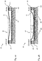
- Figs. 2a-b shows schematic diagrams of the storage device 10 according to further embodiments.
- Fig. 2a shows an out-of-plane, i.e. vertically arranged, version of the storage device 10 and Fig. 2b shows an in-plane, i.e. horizontally arranged, version of the storage device 10.
- the out-of-plane arrangement of the storage device 11, as shown in Fig. 2b has the advantage that a surface area that is occupied by the actuator 15 can be decreased with respect to the planar arrangement.
- a larger number of storage devices 10 could be integrated in a certain area.
- each out-of-plane storage device could have a tape 11 with a shorter length, leading to an overall higher area enhancement and/or lower access times.
- the pulling electrodes 16 are arranged at a further distance from the tape 11 than the clamping electrodes 17.
- the pulling electrodes 16 are recessed with respect to the clamping electrodes 17 to support the movement of the tape.
- each pulling electrode 16 can be configured to deform a section of the tape 11 by pulling said section away from a longitudinal axis of the tape 11. This deformation can result in a pulling force on the tape 11 towards the activated pulling electrode 16.
- the tape 11 is only pulled from the other (not-clamped) side resulting in a lateral movement of the non-clamped side of the tape 11 towards the pulling electrode 16.
- the tape 11 may exhibit an internal stiffness that, additionally, supports the tape 11 movement after this deformation.
- the deformed tape reverses the deformation due to its internal stiffness, causing a pushing force on the tape.
- the internal stiffness of the tape 11 may mostly stem from its bulk material 21, which can be polyethylene naphthalate (PEN).
- the internal stiffness of the tape 11 can be modulated by at least one additional counter-electrode (not shown in Figs. 2a and 2b ) on the opposite side of the tape, i.e. above the top side of the tape 11.
- the length of the pulling and clamping electrodes 16, 17 can be in the range of 100 nm to 10 ⁇ m. In particular, the pulling electrode 16 is longer than the clamping electrode 17.
- the storage device 10 as shown in Fig. 2b may further comprise two cavities 25 which are arranged, in the length direction, in front and behind the actuator 15, respectively. Each of these cavities 25 may receive an end part of the tape 11. In particular, the end parts of the tape 11 can be folded in each cavity, which allows reducing the form factor of the storage device 10.
- the storage device 10 may comprise a number of folding electrodes 23 that are arranged in each cavity 25.
- the folding electrodes 23 can be configured to guide a controlled stacking or folding of the tape 11 in the cavities 25.
- the actuator 15 may comprise additional stator electrodes for an increased motor control, such as capacitive displacement sensing for closed loop operation.
- the storage device 10 as shown in any one of the previous Figs. 1 , 2a and 2b can form an electrostatic shuffle driven mechanical memory device.
- Such a storage device 10 combines several advantages, in particular, when compared to other commonly used memory or actuation concepts:
- the actuator 15, in principle, can allow for an unlimited displacement range with nanometer resolution.
- the storage device 10 can be inherently shock resistant, because the tape 11 may be clamped to the actuator 15 at any point in time. This may also prevent undesired resonances and vibration rejection.
- the actuator 15 can be scalable.
- electrostatic step motors generally, have favorable scaling characteristics (max. operational frequency increases to MHz when scaling to the micro domain). Electrostatic pull and push forces in order of mN can still be reachable on the microscale. This is, particularly, an advantage over electromagnetic motors that do not scale well into the micro-domain, because they require permanent magnets and have a high energy consumption to operate.
- Fig. 3 shows a schematic diagram of a possible activation sequence of the actuator 15 of the storage device 10 according to an embodiment.
- Fig. 3 shows an actuation sequence for the pulling electrodes 16 and clamping electrodes 17 for moving the tape 11 for one step.
- the actuator 15 of the storage device 10 in Fig. 3 comprises one center clamping electrode 17-2, two outer clamping electrodes 17-1, 17-3, and two pulling electrodes 16-1, 16-2, which are arranged in-between the clamping electrodes 17-1, 17-2, 17-3.
- the activation sequence shown in Fig. 3 can be executed by any one of the storage devices 10 shown in Figs. 1 , 2a or 2b .
- step 1 the tape is clamped by the central clamping electrode 17-2, which is arranged directly below the data head 14.
- step 2 pulling electrode 16-1 is additionally activated. This causes a section of the tape 11 to be pulled into the recession of the pulling electrode 16-1 and, thus, results in a pulling of the (not-clamped) side of the tape 11 towards the pulling electrode. Thereby, the tape is laterally pulled by a length of ⁇ lateral towards the pulling electrode 16-1.
- step 3 the central clamping electrode 17-2 is deactivated and the two outer clamping electrodes 17-1 and 17-3 are activated.
- step 4 the pulling electrode 16-1 is deactivated and the pulling electrode 16-2 is activated instead, causing the tape 11 to move under the data head towards pulling electrode 16-2.
- step 5 the central clamping electrode 17-2 is reactivated and all other electrodes are deactivated, causing the tape 11 to stiffen-up and be pushed away from the central clamping electrode 17-2 by its internal stiffness.
- the steps 1 to 5 result in one movement step of the tape 11 by a lateral distance of ⁇ lateral .
- the tape can be moved under the data head 14 in a quick and precise manner.
- tape step frequencies between 1 kHz and several MHz as well as nanometer positioning accuracies over the complete displacement range of the storage medium (mm to cm) can be achieved.
- an operating mode of the actuator 15 can be set to a fine stepping mode or to a fast stepping mode, respectively.
- Figs. 4a-b shows schematic diagrams of a part of the actuator 15 of the storage device 10 operating in two different modes according to an embodiment.
- Fig. 4a shows the actuator 15 in the fine stepping mode
- Fig. 4b shows the actuator 15 in the fast stepping mode.
- Figs. 4a and 4b show a part of the actuator with one pulling electrode 16 and two clamping electrodes 17.
- the pulling electrode 16 is arranged in a recess 41 of height h clamp with respect to the clamping electrodes 17 and has a length of L. Further, a dielectric layer 43 of thickness t diel is arranged over the pulling electrode 16.
- the left clamping electrode 17 is activated (clamped) and the right clamping electrode 17 is deactivated (roller).
- the pulling voltage may be smaller than a threshold value.
- the threshold value can correspond to the pulling voltage V pull-in that is required so that the tape 11 is in contact with the dielectric layer 43, i.e. the tape 11 is pulled to the bottom of the recess 41 and touches said bottom.
- the first force is the electrostatic force that causes the deformation of the tape 11.
- ⁇ o is the vacuum permittivity
- V is the voltage applied to the pulling electrode
- w is the deflection of the tape 11 towards the pulling electrode
- E tape is the Young's modulus of the tape 11 and I tape is the area moment of inertia of the tape 11.
- the step size of the tape 11 can be minimized, by reducing the voltage applied to the pulling electrode 16 and, thus, the deflection w of the tape 11. In this way, a nanometer resolution position control with respect to the data head 14 may be achieved over the complete displacement range of the storage medium, which can be in the range from millimeters to centimeters.
- the mechanical stiffness (spring constant) of the tape 11 is defined by the two non-contact regions 45, each having a length of L eff /2.
- the tape speed in the fast stepping mode can be enhanced by enhancing the voltage applied to the pulling electrode 16 and, thus, decreasing the size of the non-contact region L eff , causing an enhancement of the lateral displacement ⁇ lateral .
- high velocities ( ⁇ m/s) for low random access delays during memory operation ( ⁇ milliseconds) can be achieved.
- Figs. 5a-b shows schematic diagrams of a storage system 50 according to an embodiment. Thereby, Fig. 5a is a top view and Fig. 5b is a perspective view of the storage system 50.
- the storage system 50 comprises a plurality of storage devices 10 embedded in a substrate 51.
- the plurality of storage devices 10 can, thereby, be arranged according to a square lattice with an x-pitch and a y-pitch.
- Such a storage system 50 can form a data memory, e.g. for a handheld device.
- the storage devices 10 can be arranged vertically, according to an out-of-plane arrangement, to increase the density of the storage devices 10.
- each storage device 10 can be embedded in a cavity of the substrate 51 in a vertical manner.
- Each of the storage devices 10 of the system 50 may comprise an actuator 15 which can move (push/pull operation) the flexible tape 11 (nanotape or nanotube) over a data head 14.
- the required tape 11 length can be dependent on the density of the storage devices 10.
- the typical in-plane dimension of the storage device 10 is of the order of microns, while the length of the tape 11 can be varied from millimeters to centimeters. In this way, tape 11 densities of 10 3 to 10 4 /mm 2 can be achieved.
- Fig. 6 shows a line chart highlighting the relationship between the tape 11 dimensions and the arrangement of the storage devices 10 in the storage system 50 according to an embodiment.
- Fig. 6 shows the relationship between the tape 11 length and the x-pitch of the storage devices 10 in a storage system 50 as shown in Figs. 5a or 5b .
- Fig. 6 relates to a storage system 50 with an in-plane storage density of 1 Tb/mm 2 .
- a bit pitch of 30 nm and a y-pitch driver efficiency (see Fig. 5 ) of 0.8 is assumed.
- Folding strategies can allow for longer tapes or tubes to be enclosed in low-profile memory packages ( ⁇ 5 mm thickness).
- scaling When scaling down the size of each storage device 10, more devices 10 can be present in the same overall area. If the total storage capacity is fixed, for example to 1 Tb/mm 2 , the length of the tape 11 can be decreased for each storage device 10. Eventually when scaling to a critical dimension, the tape 11 lengths for a certain storage density becomes shorter than half the height of the storage system 50. As this point, no tape folding is required (indicated by the dashed line in Fig. 6 ), thus, simplifying the implementation.
- Fig. 7 shows a schematic diagram of the storage system 50 according to another embodiment.
- Fig. 7 shows a cross-sectional view of a storage system 50, where the storage devices are embedded in a substrate 51, which comprises a silicon wafer 71, a MEMS layer 73, and top and bottom encapsulation layers 75, 77.
- the storage system 50 shown in Fig. 7 is an example for a high level implementation of the storage devices shown in Figs. 1-4 .
- the storage system 50 may comprise a large array of independent storage devices 10 (103 - 104 tapes/mm 2 ) embedded in a centimeter-sized small-outline package.
- each storage device 10 may comprise the micromechanical actuator 15 and the data head 14, e.g. in the form of a MEMS layer, and the micro/nanotape 11 which serves as the storage medium.
- Each storage device 10 may further comprise a CMOS driver circuit and an R/W circuit (silicon layer).
- the top and bottom encapsulation layers 75, 77 can provide a means of guiding the displacement of the tape 11. Additional tape storage management, i.e. tape folding, can be implemented in the encapsulation layers 75, 77.
Landscapes
- Semiconductor Memories (AREA)
- Signal Processing For Digital Recording And Reproducing (AREA)
- Engineering & Computer Science (AREA)
- Manufacturing & Machinery (AREA)
Abstract
Description
- The present disclosure relates to the field of storage devices, in particular, of storage devices configured to store data on a tape or sheet. The disclosure further relates to a storage system comprising such storage devices.
- The scaling roadmap of solid-state memory devices is currently dominated by NAND flash. NAND flash is relatively fast and has a small form factor. However, NAND flash is also relatively expensive per stored bit. In addition, the further scaling of NAND flash is becoming increasingly more difficult to achieve and may lead to an increase of its read latency.
- Other major memory technologies such as hard disk drives (HDD) and tape memory have a low cost per bit. However, they are much slower than NAND flash and have a large form factor not suitable for integration in handheld devices.
- Several alternative memory solutions have been proposed, such as micromechanical probe memory (John Heck et al., "Ultra-high density MEMS probe memory device", Microelectronic Engineering, 2010), holographic data storage (Ashley, Jonathan, et al. "Holographic data storage technology." IBM Journal of Research and Development 44.3 (2000): 341-368), or magnetic racetrack memory (Parkin, Stuart, and See-Hun Yang. "Memory on the racetrack." Nature nanotechnology 10.3 (2015): 195-198). However, these memory concepts are currently still at a research level and are not yet commercially available.
- In other words, there is still a clear need for a novel commercially viable memory technology with a form factor and speed comparable to NAND flash, but with a higher bit density and lower cost.
- Thus, it is an objective to provide an improved storage device and to provide an improved storage system. In particular, the above-mentioned disadvantages should be avoided.
- The objective is achieved by the embodiments provided in the enclosed independent claims. Advantageous implementations of the embodiments of the invention are further defined in the dependent claims.
- According to a first aspect, the present disclosure relates to a storage device, comprising a tape configured to store data; a data head configured to read and/or write data from and/or to the tape; an actuator configured to move the tape in a length direction in a step-wise manner, wherein the actuator comprises: a number of pulling electrodes, wherein each pulling electrode can be activated to exert a pulling force on the tape, and a number of clamping electrodes, wherein each clamping electrode can be activated to clamp the tape.
- This achieves the advantage that a storage device is provided that combines a small form factor, with precise and fast read/write speeds, in particular in terms of latency and throughput. These fast read/write speeds can be achieved due to an actuation mechanism that is based on moving the tape via electrostatic forces.
- The tape may be a flexible nanosheet for storing data, for example, a parallel flexible nanosheet storage. A surface area of the tape may be configured to store the data. Such a tape provides a significant area enhancement, i.e., and increased ratio of the storage medium area and the overall storage device area. Thus, such a tape allows building a storage device with a small form factor. Further, the increased ratio reduces the cost per bit of the storage device.
- The length of the tape may be varied from millimeters to centimeters.
- The actuator can be an electrostatic shuffle tape driver that is configured to move the tape in a step-wise manner. Thereby, tape step frequencies between 1 kHz and several MHz can be achieved.
- The pulling electrodes and the clamping electrodes may be configured, if activated, to excerpt an attractive electrostatic force on the tape. The actuator can be configured to move the tape in the step-wise manner by activating and deactivating the number of pulling electrodes and clamping electrodes according to a defined activation sequence. Thereby, the pulling electrodes and the clamping electrodes work together to move the tape forward or backward in the length direction. In particular, the pulling electrodes exert the pulling force on the tape which causes the tape movement while the clamping electrodes define the direction of said movement (backwards or forwards).
- The actuator can comprise at least three electrodes, namely two clamping electrodes and one pulling electrode. Preferably, the actuator comprises five or more electrodes, for example three clamping electrodes and two pulling electrodes.
- In an embodiment, the pulling electrodes and the clamping electrodes are alternately arranged along the length of the tape.
- In an embodiment, the tape comprises a conductive layer on a bottom side of the tape, which is configured to act as a counter electrode for the pulling electrodes and clamping electrodes, respectively. This achieves the advantage that the tape can be moved efficiently by the actuator based on electrostatic forces.
- In an embodiment, the pulling electrodes and the clamping electrodes are arranged below the bottom side of the tape facing the conductive layer.
- In an embodiment, the pulling electrodes are arranged at a further distance from the tape than the clamping electrodes.
- In an embodiment, if activated, each pulling electrode is configured to deform a section of the tape by pulling said section away from a longitudinal axis of the tape, wherein said deformation causes the pulling force on the tape. This achieves the advantage that the tape can be efficiently moved by the actuator.
- In particular, the tape exhibits an internal stiffness that additionally supports the movement of the tape. For example, after the pulling electrode is deactivated, the deformed tape reverses the deformation due its internal stiffness, causing an additional pushing force on the tape which supports the tape movement.
- In an embodiment, the actuator is configured to move the tape in a first direction by subsequently:
- a) activating a first clamping electrode of the number of clamping electrodes;
- b) activating a pulling electrode of the number of pulling electrodes that is arranged behind said first clamping electrode relative to the first direction;
- c) activating a second clamping electrode of the number of clamping electrodes that is arranged behind said pulling electrode relative to the first direction and simultaneously or subsequently deactivating said first clamping electrode; and
- d) deactivating said pulling electrode.
- The above sequence requires a minimum of three electrodes, namely two clamping electrodes and one pulling electrodes. For example, the actuator comprises five electrodes, three clamping and two pulling electrodes, and the above sequence is expanded taking into account the additional electrodes.
- In an embodiment, the actuator is configured to activate each clamping electrode by applying a clamping voltage to the clamping electrode, and the actuator is configured to activate each pulling electrode by applying a pulling voltage to the pulling electrode.
- In an embodiment, the actuator is configured to control a movement speed of the tape by adjusting the pulling voltage and/or by adjusting an activation frequency of the pulling electrodes and clamping electrodes, respectively. This achieves the advantage that the tape can be moved quickly and precisely depending on a current requirement.
- For example, the storage device can be set to a fine stepping mode, which is defined by a pulling voltage that is smaller than a threshold value. In this fine stepping mode, the step size of the tape movement is reduced allowing for nanometer resolution position control with respect to the data head. Alternatively, the storage device can be set to a fast stepping mode, which is defined by a pulling voltage that is larger than the threshold value. In the fast stepping mode the movement speed of the tape is increased, e.g. to achieve low random access delays during memory operation.
- In an embodiment, the tape further comprises a bulk material, preferably polyethylene naphthalate, PEN.
- In an embodiment, one or more surface regions of the tape are configured to store the data.
- For example, the surface region of the tape comprises a functional layer that can be read out / written to by the data head.
- In an embodiment, the data head is arranged over a top side of the tape opposite to the bottom side.
- In particular, the data head is arranged over the surface regions that store the data.
- In an embodiment, in a first mode of the storage device, the data head is configured to read and/or write data from and/or to the tape while the tape is stationary; and, in a second mode of the storage device, the data head is configured to read and/or write data from and/or to the tape while the tape is moving.
- In an embodiment, the storage device further comprises two cavities which are arranged, in the length direction, in front and behind the actuator, respectively; wherein each cavity is configured to receive a part of the tape, in particular an end part of the tape.
- In an embodiment, the storage device is configured to fold the tape in each cavity. This achieves the advantage that the overall size of the storage device can be reduced. In particular, a tape with a length of up to 10 mm can be folded to a much smaller size. In particular, the cavity only needs to be big enough to accommodate the folded tape.
- In an embodiment, the storage device further comprises a number of folding electrodes arranged in each cavity, wherein the folding electrodes are configured to fold the tape. This achieves the advantage that the tape can be folded and unfolded in an efficient manner for a compact storage of the tape.
- According to a second aspect, the present disclosure relates to a storage system comprising a plurality of storage devices according to the first aspect of the present disclosure embedded in a substrate.
- Embodiments of the invention will be explained in the followings together with the figures.
- Fig. 1
- shows a schematic diagram of a storage device according to an embodiment;
- Figs. 2a-b
- shows schematic diagrams of a storage device according to further embodiments;
- Fig. 3
- shows a schematic diagram of a possible activation sequence of an actuator of a storage device according to an embodiment;
- Figs. 4a-b
- shows schematic diagrams of an actuator of a storage device operating in two different modes according to an embodiment;
- Figs. 5a-b
- shows schematic diagrams of a storage system according to an embodiment;
- Fig. 6
- shows a chart of the relationship between the dimensions of a tape and the arrangement of storage devices in a storage system according to an embodiment; and
- Fig. 7
- shows a schematic diagram of a storage system according to an embodiment.
-
Fig. 1 shows a schematic diagram of astorage device 10 according to an embodiment. - The
storage device 10 comprises atape 11 configured to store data, adata head 14 configured to read and/or write data from and/or to thetape 11, and anactuator 15 configured to move thetape 11 in a length direction in a step-wise manner. Theactuator 15 comprises a number of pullingelectrodes 16, wherein each pullingelectrode 16 can be activated to exert a pulling force on thetape 11, and a number of clampingelectrodes 17, wherein each clampingelectrode 17 can be activated to clamp thetape 11. - The
actuator 15 may be a linear stepper motor that translates mechanical deformation of thetape 11, i.e. bending, into a net forward or backward displacement. - The pulling
electrodes 16 and the clampingelectrodes 17 may be configured, if activated, to excerpt an attractive electrostatic force on thetape 11. Theactuator 15 can be configured to move the tape in the step-wise manner by activating and deactivating the number of pullingelectrodes 16 and clampingelectrodes 17 according to a defined activation sequence. - Each of the pulling
electrodes 16 respectively clampingelectrodes 17 is activated by applying a defined pulling voltage respectively clamping voltage to theelectrodes - The storage device 100 that is depicted in
Fig. 1 comprises three clampingelectrodes 17 and two pullingelectrodes 16, which are alternately arranged along the length of thetape 11. However, a different number of pulling and clampingelectrodes actuator 15 comprises at least one pullingelectrode 16 and two clampingelectrodes 17 to be able to move the tape. - The
tape 11 maybe a flexible micro- or nanosheet for storing data, for example, a parallel flexible nanosheet storage. Thetape 11 can also be a tube or a rod with a certain flexibility that allows deformation. The length of thetape 11 may be varied from millimeters to centimeters. - The
tape 11 can be made of a polymer film or foil, for example polyethylene naphthalate or polyimide. - The
tape 11 can comprise a functional layer for data storage on its top side for example, the functional layer may comprise a storage element that can be read out / written to by the data head. - The
tape 11 may be configured to store data based on various different storage strategies, for example immobilized charges (similar to flash), topographic storage (e.g., generated by thermomechanical indentation of the tape surface), phase-change storage, magnetic storage, ferro-electric storage, resistive storage or electromechanical storage. The data head 14 can be configured to read/write data from/to thetape 11 according to the storage strategy. The data head 14 can be a read/write array. - The data head 14 can be arranged over the top side of the
tape 11 in adata module 13 of thestorage device 10. Thedata module 13 can be comprised in or connected to theactuator 15. - The
tape 11, preferably, comprises aconductive layer 12 on its bottom side. Thisconductive layer 12 may be configured as a counter electrode for the electrostatic actuation by the pullingelectrodes 16 and clampingelectrodes 17, which are arranged below the bottom side of thetape 11. Theconductive layer 12 can be a continuous metallic thin film or an intrinsically conductive polymer (ICP) film. - A stepped or latched operation of the
actuator 15 is performed by sequentially applying AC or DC voltages (in the range of 0.1 to 100 volt) between the clamping respectively pullingelectrodes tape 11. -
Figs. 2a-b shows schematic diagrams of thestorage device 10 according to further embodiments. - Thereby,
Fig. 2a shows an out-of-plane, i.e. vertically arranged, version of thestorage device 10 andFig. 2b shows an in-plane, i.e. horizontally arranged, version of thestorage device 10. - The out-of-plane arrangement of the
storage device 11, as shown inFig. 2b , has the advantage that a surface area that is occupied by theactuator 15 can be decreased with respect to the planar arrangement. Thus, a larger number ofstorage devices 10 could be integrated in a certain area. Thereby, each out-of-plane storage device could have atape 11 with a shorter length, leading to an overall higher area enhancement and/or lower access times. - In the
storage device 10 shown inFig. 2a and 2b , the pullingelectrodes 16 are arranged at a further distance from thetape 11 than the clampingelectrodes 17. In particular, the pullingelectrodes 16 are recessed with respect to the clampingelectrodes 17 to support the movement of the tape. - For example, if activated, each pulling
electrode 16 can be configured to deform a section of thetape 11 by pulling said section away from a longitudinal axis of thetape 11. This deformation can result in a pulling force on thetape 11 towards the activated pullingelectrode 16. By clamping thetape 11 on one side of the activated pullingelectrode 16, thetape 11 is only pulled from the other (not-clamped) side resulting in a lateral movement of the non-clamped side of thetape 11 towards the pullingelectrode 16. - Furthermore, the
tape 11 may exhibit an internal stiffness that, additionally, supports thetape 11 movement after this deformation. In particular, after the pullingelectrode 16 is deactivated again, the deformed tape reverses the deformation due to its internal stiffness, causing a pushing force on the tape. By clamping thetape 11 on the other side of the deactivated pullingelectrode 16, the internal stiffness pushes thetape 11 further in the length direction. The internal stiffness of thetape 11 may mostly stem from its bulk material 21, which can be polyethylene naphthalate (PEN). - Further, the internal stiffness of the
tape 11 can be modulated by at least one additional counter-electrode (not shown inFigs. 2a and 2b ) on the opposite side of the tape, i.e. above the top side of thetape 11. - The length of the pulling and clamping
electrodes electrode 16 is longer than the clampingelectrode 17. - The
storage device 10 as shown inFig. 2b may further comprise twocavities 25 which are arranged, in the length direction, in front and behind theactuator 15, respectively. Each of thesecavities 25 may receive an end part of thetape 11. In particular, the end parts of thetape 11 can be folded in each cavity, which allows reducing the form factor of thestorage device 10. - The
storage device 10 may comprise a number offolding electrodes 23 that are arranged in eachcavity 25. Thefolding electrodes 23 can be configured to guide a controlled stacking or folding of thetape 11 in thecavities 25. - Furthermore, the
actuator 15 may comprise additional stator electrodes for an increased motor control, such as capacitive displacement sensing for closed loop operation. - The
storage device 10 as shown in any one of the previousFigs. 1 ,2a and 2b can form an electrostatic shuffle driven mechanical memory device. Such astorage device 10 combines several advantages, in particular, when compared to other commonly used memory or actuation concepts: - Firstly, the
storage device 10, especially theactuator 15 can be compatible with common photolithographic fabrication processes and can, thus, be produced quickly and at low costs. - Secondly, there are only limited requirements on the storage medium. The
flexible tape 11, for example, only requires fragments with continuous conductive film on its bottom side, which are easy to generate. There is, preferably, no need for structured metallic or high-k islands on thetape 11. - Further, the
actuator 15, in principle, can allow for an unlimited displacement range with nanometer resolution. In addition, thestorage device 10 can be inherently shock resistant, because thetape 11 may be clamped to theactuator 15 at any point in time. This may also prevent undesired resonances and vibration rejection. - Lastly, the
actuator 15 can be scalable. In particular, electrostatic step motors, generally, have favorable scaling characteristics (max. operational frequency increases to MHz when scaling to the micro domain). Electrostatic pull and push forces in order of mN can still be reachable on the microscale. This is, particularly, an advantage over electromagnetic motors that do not scale well into the micro-domain, because they require permanent magnets and have a high energy consumption to operate. -
Fig. 3 shows a schematic diagram of a possible activation sequence of theactuator 15 of thestorage device 10 according to an embodiment. - In particular,
Fig. 3 shows an actuation sequence for the pullingelectrodes 16 and clampingelectrodes 17 for moving thetape 11 for one step. Theactuator 15 of thestorage device 10 inFig. 3 comprises one center clamping electrode 17-2, two outer clamping electrodes 17-1, 17-3, and two pulling electrodes 16-1, 16-2, which are arranged in-between the clamping electrodes 17-1, 17-2, 17-3. The activation sequence shown inFig. 3 can be executed by any one of thestorage devices 10 shown inFigs. 1 ,2a or 2b . - In a first step (step 1), the tape is clamped by the central clamping electrode 17-2, which is arranged directly below the
data head 14. - In a second step (step 2), pulling electrode 16-1 is additionally activated. This causes a section of the
tape 11 to be pulled into the recession of the pulling electrode 16-1 and, thus, results in a pulling of the (not-clamped) side of thetape 11 towards the pulling electrode. Thereby, the tape is laterally pulled by a length of Δlateral towards the pulling electrode 16-1. - In a third step (step 3), the central clamping electrode 17-2 is deactivated and the two outer clamping electrodes 17-1 and 17-3 are activated.
- In a fourth step (step 4), the pulling electrode 16-1 is deactivated and the pulling electrode 16-2 is activated instead, causing the
tape 11 to move under the data head towards pulling electrode 16-2. - In a fifth and final step (step 5), the central clamping electrode 17-2 is reactivated and all other electrodes are deactivated, causing the
tape 11 to stiffen-up and be pushed away from the central clamping electrode 17-2 by its internal stiffness. - The
steps 1 to 5 result in one movement step of thetape 11 by a lateral distance of Δlateral. By cyclically repeating steps 1-5, the tape can be moved under the data head 14 in a quick and precise manner. For example, tape step frequencies between 1 kHz and several MHz as well as nanometer positioning accuracies over the complete displacement range of the storage medium (mm to cm) can be achieved. - By regulating the pulling voltage that is applied to the pulling electrodes 16-1, 16-2, an operating mode of the
actuator 15 can be set to a fine stepping mode or to a fast stepping mode, respectively. -
Figs. 4a-b shows schematic diagrams of a part of theactuator 15 of thestorage device 10 operating in two different modes according to an embodiment. In particular,Fig. 4a shows theactuator 15 in the fine stepping mode andFig. 4b shows theactuator 15 in the fast stepping mode. -
Figs. 4a and 4b show a part of the actuator with one pullingelectrode 16 and two clampingelectrodes 17. The pullingelectrode 16 is arranged in arecess 41 of height hclamp with respect to the clampingelectrodes 17 and has a length of L. Further, adielectric layer 43 of thickness tdiel is arranged over the pullingelectrode 16. In bothFigs. 4a and 4b , theleft clamping electrode 17 is activated (clamped) and theright clamping electrode 17 is deactivated (roller). - In the fine stepping mode (
Fig. 4a ), the pulling voltage may be smaller than a threshold value. The threshold value can correspond to the pulling voltage Vpull-in that is required so that thetape 11 is in contact with thedielectric layer 43, i.e. thetape 11 is pulled to the bottom of therecess 41 and touches said bottom. - In particular, when the pulling
electrode 16 is activated, two forces are acting on thetape 11. The first force is the electrostatic force that causes the deformation of thetape 11. In particular, the first force is a "surface force" or "pressure force", i.e. normalized to the surface of the pullingelectrodes 16, and can be described by:
- Here, εo is the vacuum permittivity, V is the voltage applied to the pulling
electrode 16, w is the deflection of thetape 11 towards the pullingelectrode 16, and geff is a factor that is calculated by:
dielectric layer 43. The second force is a restoring force due to the internal stiffness of thetape 11 that can be described by:
- Here, Etape is the Young's modulus of the
tape 11 and Itape is the area moment of inertia of thetape 11. - If the pulling
electrode 16 is activated thetape 11 is pulled down until a force balance (qmech + qel = o) is reached. Solving the force balance equation for the deflection w, allows to calculate the distance by which the tape is moved in a length direction in each movement step by: Δ lateral = 2.44 · w 2/L. - In the fine stepping mode shown in
Fig. 4a , the step size of thetape 11 can be minimized, by reducing the voltage applied to the pullingelectrode 16 and, thus, the deflection w of thetape 11. In this way, a nanometer resolution position control with respect to thedata head 14 may be achieved over the complete displacement range of the storage medium, which can be in the range from millimeters to centimeters. - In the fast stepping mode (
Fig. 4b ), the pulling voltage may exceed the threshold value. Therefore, a section of the deformed tape of length Lcontact is in contact with the bottom of therecess 41, wherein Lcontact = L - Leff. Thus, the mechanical stiffness (spring constant) of thetape 11 is defined by the twonon-contact regions 45, each having a length of Leff/2. - This changes the electrostatic force that causes the deformation of the
tape 11 to:

- Solving the force balance equation for the non-contact region Leff, allows to calculate the distance by which the tape is moved in length direction in each step according to:

- In particular, in the fast stepping mode the tape speed can be enhanced by enhancing the voltage applied to the pulling
electrode 16 and, thus, decreasing the size of the non-contact region Leff, causing an enhancement of the lateral displacement Δlateral. Thereby, high velocities (∼ m/s) for low random access delays during memory operation (∼ milliseconds) can be achieved. -
Figs. 5a-b shows schematic diagrams of astorage system 50 according to an embodiment. Thereby,Fig. 5a is a top view andFig. 5b is a perspective view of thestorage system 50. - The
storage system 50 comprises a plurality ofstorage devices 10 embedded in asubstrate 51. The plurality ofstorage devices 10 can, thereby, be arranged according to a square lattice with an x-pitch and a y-pitch. - Such a
storage system 50 can form a data memory, e.g. for a handheld device. - The
storage devices 10 can be arranged vertically, according to an out-of-plane arrangement, to increase the density of thestorage devices 10. For example, eachstorage device 10 can be embedded in a cavity of thesubstrate 51 in a vertical manner. - Each of the
storage devices 10 of thesystem 50 may comprise anactuator 15 which can move (push/pull operation) the flexible tape 11 (nanotape or nanotube) over adata head 14. For a fixed in-plane density, the requiredtape 11 length can be dependent on the density of thestorage devices 10. The typical in-plane dimension of thestorage device 10 is of the order of microns, while the length of thetape 11 can be varied from millimeters to centimeters. In this way,tape 11 densities of 103 to 104/mm2 can be achieved. -
Fig. 6 shows a line chart highlighting the relationship between thetape 11 dimensions and the arrangement of thestorage devices 10 in thestorage system 50 according to an embodiment. - In particular,
Fig. 6 shows the relationship between thetape 11 length and the x-pitch of thestorage devices 10 in astorage system 50 as shown inFigs. 5a or 5b . For example,Fig. 6 relates to astorage system 50 with an in-plane storage density of 1 Tb/mm2. Thereby, a bit pitch of 30 nm and a y-pitch driver efficiency (seeFig. 5 ) of 0.8 is assumed. Folding strategies can allow for longer tapes or tubes to be enclosed in low-profile memory packages (< 5 mm thickness). - When scaling down the size of each
storage device 10,more devices 10 can be present in the same overall area. If the total storage capacity is fixed, for example to 1 Tb/mm2, the length of thetape 11 can be decreased for eachstorage device 10. Eventually when scaling to a critical dimension, thetape 11 lengths for a certain storage density becomes shorter than half the height of thestorage system 50. As this point, no tape folding is required (indicated by the dashed line inFig. 6 ), thus, simplifying the implementation. Here, scaling may refer to equal scaling of absolute X-pitch and Y-pitch as indicated inFig. 5a , e.g. assuming the maximum width of the tape is 80% of the full Y-pitch (∼ Y-efficiency = 80%). -
Fig. 7 shows a schematic diagram of thestorage system 50 according to another embodiment. - In particular,
Fig. 7 shows a cross-sectional view of astorage system 50, where the storage devices are embedded in asubstrate 51, which comprises asilicon wafer 71, aMEMS layer 73, and top and bottom encapsulation layers 75, 77. - The
storage system 50 shown inFig. 7 is an example for a high level implementation of the storage devices shown inFigs. 1-4 . Thestorage system 50 may comprise a large array of independent storage devices 10 (103 - 104 tapes/mm2) embedded in a centimeter-sized small-outline package. Thereby, eachstorage device 10 may comprise themicromechanical actuator 15 and thedata head 14, e.g. in the form of a MEMS layer, and the micro/nanotape 11 which serves as the storage medium. Eachstorage device 10 may further comprise a CMOS driver circuit and an R/W circuit (silicon layer). The top and bottom encapsulation layers 75, 77 can provide a means of guiding the displacement of thetape 11. Additional tape storage management, i.e. tape folding, can be implemented in the encapsulation layers 75, 77.
Claims (17)
- A storage device (10), comprising:a tape (11) configured to store data;
a data head (14) configured to read and/or write data from and/or to the tape (11); andan actuator (15) configured to move the tape (11) in a length direction in a step-wise manner, wherein the actuator (15) comprises:- a number of pulling electrodes (16), wherein each pulling electrode (16) can be activated to exert a pulling force on the tape (11), and- a number of clamping electrodes (17), wherein each clamping electrode (17) can be activated to clamp the tape (11). - The storage device (10) of claim 1, wherein the pulling electrodes (16) and the clamping electrodes (17) are alternately arranged along the length of the tape (11).
- The storage device (10) of claim 1 or 2, wherein the tape (11) comprises a conductive layer (12) on a bottom side of the tape (11), which is configured to act as a counter electrode for the pulling electrodes (16) and clamping electrodes (17), respectively.
- The storage device (10) of claim 3, wherein the pulling electrodes (16) and the clamping electrodes (17) are arranged below the bottom side of the tape (11) facing the conductive layer (12).
- The storage device (10) of any one of the preceding claims, wherein the pulling electrodes (16) are arranged at a further distance from the tape (11) than the clamping electrodes (17).
- The storage device (10) of any one of the preceding claims, wherein, if activated, each pulling electrode (16) is configured to deform a section of the tape (11) by pulling said section away from a longitudinal axis of the tape (11), wherein said deformation causes the pulling force on the tape (11).
- The storage device (10) of any one of the preceding claims, wherein the actuator (15) is configured to move the tape (11) in a first direction by subsequently:a) activating a first clamping electrode (17) of the number of clamping electrodes (17);b) activating a pulling electrode (16) of the number of pulling electrodes (16) that is arranged behind said first clamping electrode (17) relative to the first direction;c) activating a second clamping electrode (17) of the number of clamping electrodes (17) that is arranged behind said pulling electrode (16) relative to the first direction and simultaneously or subsequently deactivating said first clamping electrode (17); andd) deactivating said pulling electrode (16).
- The storage device (10) of any one of the preceding claims, wherein the actuator (15) is configured to activate each clamping electrode (17) by applying a clamping voltage to the clamping electrode (17), and wherein the actuator (15) is configured to activate each pulling electrode (16) by applying a pulling voltage to the pulling electrode (16).
- The storage device (10) of claim 8, wherein the actuator (15) is configured to control a movement speed of the tape (11) by adjusting the pulling voltage and/or by adjusting an activation frequency of the pulling electrodes (16) and clamping electrodes (17), respectively.
- The storage device (10) of any one of the preceding claims, wherein the tape (11) further comprises a bulk material (21), preferably polyethylene naphthalate, PEN.
- The storage device (10) of any one of the preceding claims, wherein one or more surface regions of the tape (11) are configured to store the data.
- The storage device (10) of any one of the preceding claims, wherein the data head (14) is arranged over a top side of the tape (11) opposite to the bottom side.
- The storage device (10) of any one of the preceding claims, wherein, in a first mode of the storage device (10), the data head (14) is configured to read and/or write data from and/or to the tape (11) while the tape (11) is stationary; and wherein, in a second mode of the storage device (10), the data head (14) is configured to read and/or write data from and/or to the tape (11) while the tape (11) is moving.
- The storage device (10) of any one of the preceding claims, further comprising:two cavities (25) which are arranged, in the length direction, in front and behind the actuator (15), respectively;wherein each cavity (25) is configured to receive a part of the tape (11), in particular an end part of the tape (11).
- The storage device (10) of claim 14, wherein the storage device (10) is configured to fold the tape (11) in each cavity (25).
- The storage device (10) of claim 15, further comprising:
a number of folding electrodes (23) arranged in each cavity (25), wherein the folding electrodes (23) are configured to fold the tape (11). - A storage system (50) comprising a plurality of storage devices (10) according to any one of the preceding claims embedded in a substrate (51).
Priority Applications (2)
| Application Number | Priority Date | Filing Date | Title |
|---|---|---|---|
| EP20217355.5A EP4020471B1 (en) | 2020-12-28 | 2020-12-28 | Tape based storage device |
| US17/645,107 US11462244B2 (en) | 2020-12-28 | 2021-12-20 | Tape based storage device having actuator including pulling and clamping electrodes |
Applications Claiming Priority (1)
| Application Number | Priority Date | Filing Date | Title |
|---|---|---|---|
| EP20217355.5A EP4020471B1 (en) | 2020-12-28 | 2020-12-28 | Tape based storage device |
Publications (2)
| Publication Number | Publication Date |
|---|---|
| EP4020471A1 true EP4020471A1 (en) | 2022-06-29 |
| EP4020471B1 EP4020471B1 (en) | 2024-09-11 |
Family
ID=73943244
Family Applications (1)
| Application Number | Title | Priority Date | Filing Date |
|---|---|---|---|
| EP20217355.5A Active EP4020471B1 (en) | 2020-12-28 | 2020-12-28 | Tape based storage device |
Country Status (2)
| Country | Link |
|---|---|
| US (1) | US11462244B2 (en) |
| EP (1) | EP4020471B1 (en) |
Citations (3)
| Publication number | Priority date | Publication date | Assignee | Title |
|---|---|---|---|---|
| JP2000251348A (en) * | 1999-02-26 | 2000-09-14 | Sony Corp | Electrostatic capstan, electrostatic capstan mechanism, travel control method for tape-shaped recording medium, and signal processing device for tape-shaped recording medium |
| US20120228991A1 (en) * | 2011-02-07 | 2012-09-13 | Vranish John M | Tape muscle |
| EP3836384A1 (en) * | 2019-12-10 | 2021-06-16 | Imec VZW | Storage device using a tape for storing data |
Family Cites Families (10)
| Publication number | Priority date | Publication date | Assignee | Title |
|---|---|---|---|---|
| US2831678A (en) | 1954-12-28 | 1958-04-22 | Soroban Engineering Inc | Electrostatic tape drive |
| US2956718A (en) | 1955-04-15 | 1960-10-18 | Honeywell Regulator Co | Bidirectional tape transport apparatus |
| US3183494A (en) | 1956-08-31 | 1965-05-11 | Sperry Rand Corp | Random access memory systems |
| US3057529A (en) | 1960-09-20 | 1962-10-09 | Ibm | Tape transport apparatus |
| US3353734A (en) | 1963-04-03 | 1967-11-21 | Kinelogic Corp | Drive systems involving electrostatic forces |
| GB1071702A (en) | 1964-03-02 | 1967-06-14 | Vyzk Ustav Matemat Stroju | Electrostatic driving and or braking devices for recording tapes |
| US4754185A (en) | 1986-10-16 | 1988-06-28 | American Telephone And Telegraph Company, At&T Bell Laboratories | Micro-electrostatic motor |
| US4943750A (en) | 1987-05-20 | 1990-07-24 | Massachusetts Institute Of Technology | Electrostatic micromotor |
| US5235225A (en) | 1990-08-31 | 1993-08-10 | Northwestern University | Linear electrostatic actuator with means for concatenation |
| EP2017949A1 (en) | 2007-07-16 | 2009-01-21 | Interuniversitair Microelektronica Centrum (IMEC) | Stepping actuator and method of fabrication |
-
2020
- 2020-12-28 EP EP20217355.5A patent/EP4020471B1/en active Active
-
2021
- 2021-12-20 US US17/645,107 patent/US11462244B2/en active Active
Patent Citations (3)
| Publication number | Priority date | Publication date | Assignee | Title |
|---|---|---|---|---|
| JP2000251348A (en) * | 1999-02-26 | 2000-09-14 | Sony Corp | Electrostatic capstan, electrostatic capstan mechanism, travel control method for tape-shaped recording medium, and signal processing device for tape-shaped recording medium |
| US20120228991A1 (en) * | 2011-02-07 | 2012-09-13 | Vranish John M | Tape muscle |
| EP3836384A1 (en) * | 2019-12-10 | 2021-06-16 | Imec VZW | Storage device using a tape for storing data |
Non-Patent Citations (2)
| Title |
|---|
| ASHLEYJONATHAN ET AL.: "Holographic data storage technology", IBM JOURNAL OF RESEARCH AND DEVELOPMENT, vol. 44, no. 3, 2000, pages 341 - 368 |
| PARKIN, STUARTSEE-HUN YANG: "Memory on the racetrack", NATURE NANOTECHNOLOGY, vol. 10, no. 3, 2015, pages 195 - 198 |
Also Published As
| Publication number | Publication date |
|---|---|
| EP4020471B1 (en) | 2024-09-11 |
| US11462244B2 (en) | 2022-10-04 |
| US20220223175A1 (en) | 2022-07-14 |
Similar Documents
| Publication | Publication Date | Title |
|---|---|---|
| EP1530210B1 (en) | Information recording/reproducing apparatus and recording medium | |
| US7839710B2 (en) | Nano-electro-mechanical memory cells and devices | |
| US20080277718A1 (en) | 1T MEMS scalable memory cell | |
| CN108400722B (en) | A two-degree-of-freedom piezoelectric drive device and its excitation method | |
| JP2006174688A (en) | MEMS actuator | |
| CN103986365B (en) | Inertia piezoelectric motor device that multi-region drives and scanning probe microscopy and control methods | |
| EP0978832A2 (en) | System and method for forming electrostatically actuated data storage mechanisms | |
| Tsuchiya et al. | Nanoelectromechanical nonvolatile memory device incorporating nanocrystalline Si dots | |
| JP5344810B2 (en) | Information storage device using domain wall motion and manufacturing method thereof | |
| US6984862B2 (en) | Storage device with charge trapping structure and methods | |
| EP4020471B1 (en) | Tape based storage device | |
| US7547883B2 (en) | Seek-scan probe (SSP) memory including mechanism for track correction | |
| US7567019B2 (en) | Actuator system | |
| EP2211362B1 (en) | Method for controlling a micromechanical element | |
| JP4402156B2 (en) | Information storage device using probe | |
| JP2017523558A (en) | Magnetic nanomechanical devices for stiction compensation | |
| KR20200019291A (en) | Nem memory cell, nem memory device including the same and manufacturing method of nem memory cell | |
| KR20220052365A (en) | Atomic Nano Positioning Device | |
| KR100439908B1 (en) | Electrostatic micro actuator | |
| Yang et al. | Probe recording technology using novel MEMS devices | |
| JP5160299B2 (en) | Micro movable device and driving method thereof | |
| EP3836384B1 (en) | Storage device using a tape for storing data | |
| JP2000357377A (en) | Piezoelectric actuator, head support mechanism using the same, and magnetic disk drive using the same | |
| WO2007114353A1 (en) | Information storage device using probe | |
| JP2004032952A (en) | Drive |
Legal Events
| Date | Code | Title | Description |
|---|---|---|---|
| PUAI | Public reference made under article 153(3) epc to a published international application that has entered the european phase |
Free format text: ORIGINAL CODE: 0009012 |
|
| STAA | Information on the status of an ep patent application or granted ep patent |
Free format text: STATUS: THE APPLICATION HAS BEEN PUBLISHED |
|
| AK | Designated contracting states |
Kind code of ref document: A1 Designated state(s): AL AT BE BG CH CY CZ DE DK EE ES FI FR GB GR HR HU IE IS IT LI LT LU LV MC MK MT NL NO PL PT RO RS SE SI SK SM TR |
|
| STAA | Information on the status of an ep patent application or granted ep patent |
Free format text: STATUS: REQUEST FOR EXAMINATION WAS MADE |
|
| 17P | Request for examination filed |
Effective date: 20221214 |
|
| RBV | Designated contracting states (corrected) |
Designated state(s): AL AT BE BG CH CY CZ DE DK EE ES FI FR GB GR HR HU IE IS IT LI LT LU LV MC MK MT NL NO PL PT RO RS SE SI SK SM TR |
|
| GRAP | Despatch of communication of intention to grant a patent |
Free format text: ORIGINAL CODE: EPIDOSNIGR1 |
|
| STAA | Information on the status of an ep patent application or granted ep patent |
Free format text: STATUS: GRANT OF PATENT IS INTENDED |
|
| INTG | Intention to grant announced |
Effective date: 20240430 |
|
| GRAS | Grant fee paid |
Free format text: ORIGINAL CODE: EPIDOSNIGR3 |
|
| GRAA | (expected) grant |
Free format text: ORIGINAL CODE: 0009210 |
|
| STAA | Information on the status of an ep patent application or granted ep patent |
Free format text: STATUS: THE PATENT HAS BEEN GRANTED |
|
| AK | Designated contracting states |
Kind code of ref document: B1 Designated state(s): AL AT BE BG CH CY CZ DE DK EE ES FI FR GB GR HR HU IE IS IT LI LT LU LV MC MK MT NL NO PL PT RO RS SE SI SK SM TR |
|
| REG | Reference to a national code |
Ref country code: GB Ref legal event code: FG4D |
|
| REG | Reference to a national code |
Ref country code: CH Ref legal event code: EP |
|
| REG | Reference to a national code |
Ref country code: DE Ref legal event code: R096 Ref document number: 602020037472 Country of ref document: DE |
|
| REG | Reference to a national code |
Ref country code: IE Ref legal event code: FG4D |
|
| P01 | Opt-out of the competence of the unified patent court (upc) registered |
Free format text: CASE NUMBER: APP_53774/2024 Effective date: 20240927 |
|
| REG | Reference to a national code |
Ref country code: LT Ref legal event code: MG9D |
|
| PG25 | Lapsed in a contracting state [announced via postgrant information from national office to epo] |
Ref country code: NO Free format text: LAPSE BECAUSE OF FAILURE TO SUBMIT A TRANSLATION OF THE DESCRIPTION OR TO PAY THE FEE WITHIN THE PRESCRIBED TIME-LIMIT Effective date: 20241211 |
|
| REG | Reference to a national code |
Ref country code: NL Ref legal event code: MP Effective date: 20240911 |
|
| PG25 | Lapsed in a contracting state [announced via postgrant information from national office to epo] |
Ref country code: GR Free format text: LAPSE BECAUSE OF FAILURE TO SUBMIT A TRANSLATION OF THE DESCRIPTION OR TO PAY THE FEE WITHIN THE PRESCRIBED TIME-LIMIT Effective date: 20241212 Ref country code: FI Free format text: LAPSE BECAUSE OF FAILURE TO SUBMIT A TRANSLATION OF THE DESCRIPTION OR TO PAY THE FEE WITHIN THE PRESCRIBED TIME-LIMIT Effective date: 20240911 |
|
| PG25 | Lapsed in a contracting state [announced via postgrant information from national office to epo] |
Ref country code: BG Free format text: LAPSE BECAUSE OF FAILURE TO SUBMIT A TRANSLATION OF THE DESCRIPTION OR TO PAY THE FEE WITHIN THE PRESCRIBED TIME-LIMIT Effective date: 20240911 |
|
| PG25 | Lapsed in a contracting state [announced via postgrant information from national office to epo] |
Ref country code: LV Free format text: LAPSE BECAUSE OF FAILURE TO SUBMIT A TRANSLATION OF THE DESCRIPTION OR TO PAY THE FEE WITHIN THE PRESCRIBED TIME-LIMIT Effective date: 20240911 |
|
| PG25 | Lapsed in a contracting state [announced via postgrant information from national office to epo] |
Ref country code: HR Free format text: LAPSE BECAUSE OF FAILURE TO SUBMIT A TRANSLATION OF THE DESCRIPTION OR TO PAY THE FEE WITHIN THE PRESCRIBED TIME-LIMIT Effective date: 20240911 |
|
| PG25 | Lapsed in a contracting state [announced via postgrant information from national office to epo] |
Ref country code: RS Free format text: LAPSE BECAUSE OF FAILURE TO SUBMIT A TRANSLATION OF THE DESCRIPTION OR TO PAY THE FEE WITHIN THE PRESCRIBED TIME-LIMIT Effective date: 20241211 Ref country code: ES Free format text: LAPSE BECAUSE OF FAILURE TO SUBMIT A TRANSLATION OF THE DESCRIPTION OR TO PAY THE FEE WITHIN THE PRESCRIBED TIME-LIMIT Effective date: 20240911 |
|
| PG25 | Lapsed in a contracting state [announced via postgrant information from national office to epo] |
Ref country code: RS Free format text: LAPSE BECAUSE OF FAILURE TO SUBMIT A TRANSLATION OF THE DESCRIPTION OR TO PAY THE FEE WITHIN THE PRESCRIBED TIME-LIMIT Effective date: 20241211 Ref country code: NO Free format text: LAPSE BECAUSE OF FAILURE TO SUBMIT A TRANSLATION OF THE DESCRIPTION OR TO PAY THE FEE WITHIN THE PRESCRIBED TIME-LIMIT Effective date: 20241211 Ref country code: LV Free format text: LAPSE BECAUSE OF FAILURE TO SUBMIT A TRANSLATION OF THE DESCRIPTION OR TO PAY THE FEE WITHIN THE PRESCRIBED TIME-LIMIT Effective date: 20240911 Ref country code: HR Free format text: LAPSE BECAUSE OF FAILURE TO SUBMIT A TRANSLATION OF THE DESCRIPTION OR TO PAY THE FEE WITHIN THE PRESCRIBED TIME-LIMIT Effective date: 20240911 Ref country code: GR Free format text: LAPSE BECAUSE OF FAILURE TO SUBMIT A TRANSLATION OF THE DESCRIPTION OR TO PAY THE FEE WITHIN THE PRESCRIBED TIME-LIMIT Effective date: 20241212 Ref country code: FI Free format text: LAPSE BECAUSE OF FAILURE TO SUBMIT A TRANSLATION OF THE DESCRIPTION OR TO PAY THE FEE WITHIN THE PRESCRIBED TIME-LIMIT Effective date: 20240911 Ref country code: ES Free format text: LAPSE BECAUSE OF FAILURE TO SUBMIT A TRANSLATION OF THE DESCRIPTION OR TO PAY THE FEE WITHIN THE PRESCRIBED TIME-LIMIT Effective date: 20240911 Ref country code: BG Free format text: LAPSE BECAUSE OF FAILURE TO SUBMIT A TRANSLATION OF THE DESCRIPTION OR TO PAY THE FEE WITHIN THE PRESCRIBED TIME-LIMIT Effective date: 20240911 |
|
| REG | Reference to a national code |
Ref country code: AT Ref legal event code: MK05 Ref document number: 1723429 Country of ref document: AT Kind code of ref document: T Effective date: 20240911 |
|
| PG25 | Lapsed in a contracting state [announced via postgrant information from national office to epo] |
Ref country code: NL Free format text: LAPSE BECAUSE OF FAILURE TO SUBMIT A TRANSLATION OF THE DESCRIPTION OR TO PAY THE FEE WITHIN THE PRESCRIBED TIME-LIMIT Effective date: 20240911 |
|
| PG25 | Lapsed in a contracting state [announced via postgrant information from national office to epo] |
Ref country code: PT Free format text: LAPSE BECAUSE OF FAILURE TO SUBMIT A TRANSLATION OF THE DESCRIPTION OR TO PAY THE FEE WITHIN THE PRESCRIBED TIME-LIMIT Effective date: 20250113 Ref country code: IS Free format text: LAPSE BECAUSE OF FAILURE TO SUBMIT A TRANSLATION OF THE DESCRIPTION OR TO PAY THE FEE WITHIN THE PRESCRIBED TIME-LIMIT Effective date: 20250111 |
|
| PG25 | Lapsed in a contracting state [announced via postgrant information from national office to epo] |
Ref country code: RO Free format text: LAPSE BECAUSE OF FAILURE TO SUBMIT A TRANSLATION OF THE DESCRIPTION OR TO PAY THE FEE WITHIN THE PRESCRIBED TIME-LIMIT Effective date: 20240911 Ref country code: SM Free format text: LAPSE BECAUSE OF FAILURE TO SUBMIT A TRANSLATION OF THE DESCRIPTION OR TO PAY THE FEE WITHIN THE PRESCRIBED TIME-LIMIT Effective date: 20240911 |
|
| PG25 | Lapsed in a contracting state [announced via postgrant information from national office to epo] |
Ref country code: EE Free format text: LAPSE BECAUSE OF FAILURE TO SUBMIT A TRANSLATION OF THE DESCRIPTION OR TO PAY THE FEE WITHIN THE PRESCRIBED TIME-LIMIT Effective date: 20240911 Ref country code: AT Free format text: LAPSE BECAUSE OF FAILURE TO SUBMIT A TRANSLATION OF THE DESCRIPTION OR TO PAY THE FEE WITHIN THE PRESCRIBED TIME-LIMIT Effective date: 20240911 |
|
| PG25 | Lapsed in a contracting state [announced via postgrant information from national office to epo] |
Ref country code: CZ Free format text: LAPSE BECAUSE OF FAILURE TO SUBMIT A TRANSLATION OF THE DESCRIPTION OR TO PAY THE FEE WITHIN THE PRESCRIBED TIME-LIMIT Effective date: 20240911 Ref country code: PL Free format text: LAPSE BECAUSE OF FAILURE TO SUBMIT A TRANSLATION OF THE DESCRIPTION OR TO PAY THE FEE WITHIN THE PRESCRIBED TIME-LIMIT Effective date: 20240911 |
|
| PG25 | Lapsed in a contracting state [announced via postgrant information from national office to epo] |
Ref country code: SK Free format text: LAPSE BECAUSE OF FAILURE TO SUBMIT A TRANSLATION OF THE DESCRIPTION OR TO PAY THE FEE WITHIN THE PRESCRIBED TIME-LIMIT Effective date: 20240911 Ref country code: IT Free format text: LAPSE BECAUSE OF FAILURE TO SUBMIT A TRANSLATION OF THE DESCRIPTION OR TO PAY THE FEE WITHIN THE PRESCRIBED TIME-LIMIT Effective date: 20240911 |
|
| REG | Reference to a national code |
Ref country code: DE Ref legal event code: R097 Ref document number: 602020037472 Country of ref document: DE |
|
| PG25 | Lapsed in a contracting state [announced via postgrant information from national office to epo] |
Ref country code: MC Free format text: LAPSE BECAUSE OF FAILURE TO SUBMIT A TRANSLATION OF THE DESCRIPTION OR TO PAY THE FEE WITHIN THE PRESCRIBED TIME-LIMIT Effective date: 20240911 |
|
| PG25 | Lapsed in a contracting state [announced via postgrant information from national office to epo] |
Ref country code: DK Free format text: LAPSE BECAUSE OF FAILURE TO SUBMIT A TRANSLATION OF THE DESCRIPTION OR TO PAY THE FEE WITHIN THE PRESCRIBED TIME-LIMIT Effective date: 20240911 |
|
| PLBE | No opposition filed within time limit |
Free format text: ORIGINAL CODE: 0009261 |
|
| STAA | Information on the status of an ep patent application or granted ep patent |
Free format text: STATUS: NO OPPOSITION FILED WITHIN TIME LIMIT |
|
| REG | Reference to a national code |
Ref country code: CH Ref legal event code: PL |
|
| PG25 | Lapsed in a contracting state [announced via postgrant information from national office to epo] |
Ref country code: LU Free format text: LAPSE BECAUSE OF NON-PAYMENT OF DUE FEES Effective date: 20241228 |
|
| 26N | No opposition filed |
Effective date: 20250612 |
|
| GBPC | Gb: european patent ceased through non-payment of renewal fee |
Effective date: 20241228 |
|
| PG25 | Lapsed in a contracting state [announced via postgrant information from national office to epo] |
Ref country code: SE Free format text: LAPSE BECAUSE OF FAILURE TO SUBMIT A TRANSLATION OF THE DESCRIPTION OR TO PAY THE FEE WITHIN THE PRESCRIBED TIME-LIMIT Effective date: 20240911 |
|
| REG | Reference to a national code |
Ref country code: BE Ref legal event code: MM Effective date: 20241231 |
|
| PG25 | Lapsed in a contracting state [announced via postgrant information from national office to epo] |
Ref country code: BE Free format text: LAPSE BECAUSE OF NON-PAYMENT OF DUE FEES Effective date: 20241231 Ref country code: GB Free format text: LAPSE BECAUSE OF NON-PAYMENT OF DUE FEES Effective date: 20241228 |
|
| PG25 | Lapsed in a contracting state [announced via postgrant information from national office to epo] |
Ref country code: FR Free format text: LAPSE BECAUSE OF NON-PAYMENT OF DUE FEES Effective date: 20241231 |
|
| PG25 | Lapsed in a contracting state [announced via postgrant information from national office to epo] |
Ref country code: CH Free format text: LAPSE BECAUSE OF NON-PAYMENT OF DUE FEES Effective date: 20241231 |
|
| PG25 | Lapsed in a contracting state [announced via postgrant information from national office to epo] |
Ref country code: IE Free format text: LAPSE BECAUSE OF NON-PAYMENT OF DUE FEES Effective date: 20241228 |
|
| PGFP | Annual fee paid to national office [announced via postgrant information from national office to epo] |
Ref country code: DE Payment date: 20251126 Year of fee payment: 6 |