EP4020309B1 - Fingerprint apparatus, and electronic device and method for manufacturing same - Google Patents
Fingerprint apparatus, and electronic device and method for manufacturing same Download PDFInfo
- Publication number
- EP4020309B1 EP4020309B1 EP20858226.2A EP20858226A EP4020309B1 EP 4020309 B1 EP4020309 B1 EP 4020309B1 EP 20858226 A EP20858226 A EP 20858226A EP 4020309 B1 EP4020309 B1 EP 4020309B1
- Authority
- EP
- European Patent Office
- Prior art keywords
- middle frame
- collimator
- fingerprint
- disposed
- fingerprint apparatus
- Prior art date
- Legal status (The legal status is an assumption and is not a legal conclusion. Google has not performed a legal analysis and makes no representation as to the accuracy of the status listed.)
- Active
Links
Images


Classifications
-
- G—PHYSICS
- G06—COMPUTING OR CALCULATING; COUNTING
- G06V—IMAGE OR VIDEO RECOGNITION OR UNDERSTANDING
- G06V40/00—Recognition of biometric, human-related or animal-related patterns in image or video data
- G06V40/10—Human or animal bodies, e.g. vehicle occupants or pedestrians; Body parts, e.g. hands
- G06V40/12—Fingerprints or palmprints
- G06V40/13—Sensors therefor
- G06V40/1324—Sensors therefor by using geometrical optics, e.g. using prisms
-
- G—PHYSICS
- G02—OPTICS
- G02B—OPTICAL ELEMENTS, SYSTEMS OR APPARATUS
- G02B27/00—Optical systems or apparatus not provided for by any of the groups G02B1/00 - G02B26/00, G02B30/00
- G02B27/30—Collimators
-
- G—PHYSICS
- G02—OPTICS
- G02B—OPTICAL ELEMENTS, SYSTEMS OR APPARATUS
- G02B3/00—Simple or compound lenses
- G02B3/0006—Arrays
- G02B3/0037—Arrays characterized by the distribution or form of lenses
- G02B3/0056—Arrays characterized by the distribution or form of lenses arranged along two different directions in a plane, e.g. honeycomb arrangement of lenses
Definitions
- This application relates to the field of electronic device technologies, and in particular, to a fingerprint apparatus, an electronic device, and a manufacturing method thereof.
- An electronic device such as a mobile phone is used as an example.
- Information exchange between the mobile phone and a human mainly includes keyboard pressing, screen touching, wireless communication, voice input, facial recognition, fingerprint recognition, and the like.
- Fingerprint recognition has been widely used in operations such as unlocking and payment in the mobile phone for uniqueness and convenience.
- the mobile phone is used as an example.
- An existing fingerprint recognition system is usually disposed at a position at which a front physical button is located, disposed on a back, and disposed below a display screen.
- full-screen display is an important development direction and a technical selling point for future electronic devices such as a mobile phone, and an in-screen fingerprint recognition technology corresponding to full-screen display can draw more attention for user-friendliness.
- common in-screen fingerprint recognition technologies include an optical fingerprint recognition technology, a capacitive fingerprint recognition technology, an ultrasonic fingerprint recognition technology, and the like.
- CN 109 791 612 A discloses a fingerprint identification device which includes a micro- telecentric lens array group, for receiving optical signal reflected from a human finger and a fingerprint sensor set to the lower section of micro- telecentric lens array group.
- CN 208 848 221 U discloses an optical fingerprint identification device able that includes a light detection array, a first shading layer formed above the light detection array, wherein the first shading layer is provided with multiple light passing apertures, a first microlens array set to above first shading layer, wherein the first microlens array is used to converge optical signal to the multiple light passing apertures of the first shading layer, and the optical signal is transmitted to the light detection array by the multiple light passing apertures of the first shading layer.
- An installation position is flexible, and therefore a problem that a screen is scrapped due to installation of the fingerprint apparatus through attachment to the screen can be avoided.
- 01 Screen; 02: Fastening frame; 03: Battery region; 04: Non-battery region; 05: Fingerprint apparatus; 051: Image sensor; 052: Collimation component; 053: Lens structure; 100: Fingerprint apparatus; 101: Fingerprint image sensor; 102: Collimator; 1021: Collimator hole; 103: First microlens group; 1031: First microlens unit; 104: Second microlens group; 1041: Second microlens unit; 105: Flexible circuit board; 200: Display screen; 300: Middle frame; 301: Groove; 302: Middle frame body; 303: Middle frame support member; 304: Mounting hole; 400: Battery module; 500: Battery region; and 600: Non-battery region.
- FIG. 1 is a schematic stacking diagram of a typical architecture of an existing electronic device such as a mobile phone.
- the architecture includes a screen 01 and a fastening frame 02.
- Space below the fastening frame 02 may be divided into a battery region 03 and a non-battery region 04 based on different disposed parts.
- the battery region 03 is used to accommodate a power supply.
- the non-battery region 04 is used to accommodate other optional electronic elements such as a circuit board, a speaker box, a motor, and a camera.
- a fingerprint apparatus is placed below the screen 01.
- the fingerprint apparatus may be fastened to the screen 01 or the fastening frame 02.
- the fingerprint apparatus may be located above the battery region 03 or the non-battery region 04. Due to a limitation of a structure or the prior art, in the foregoing solution of positions for disposing the fingerprint apparatus, there is a possibility that the fingerprint apparatus cannot be disposed at some of the positions, or there may be some problems after implementation. For example, when the fingerprint apparatus is attached to the screen 01 for assembly, there is a problem of relatively high costs due to poor attachment, and a limited thickness of the fingerprint apparatus affects a battery capacity or results in an increase in a thickness of the entire device. When the fingerprint apparatus is relatively thick, the fingerprint apparatus can be disposed only above the non-battery region 04.
- a requirement for a large-area in-screen fingerprint cannot be met due to a limited area of the non-battery region 04.
- a direction from the fastening frame to the screen is an upward direction
- a direction from the screen to the fastening frame is a downward direction.
- the fingerprint apparatus may be located above the battery region 03. It may be understood that the fingerprint apparatus is located above the battery region in the thickness direction of the electronic device, and an orthographic projection of the fingerprint apparatus on the fastening frame is located in a region of an orthographic projection of the battery region on the fastening frame. Correspondingly, the fingerprint apparatus may be located above the non-battery region 04.
- the fingerprint apparatus is located above the non-battery region in the thickness direction of the electronic device, and an orthographic projection of the fingerprint apparatus on the fastening frame is located in a region of an orthographic projection of the battery region on the fastening frame.
- the fingerprint apparatus 05 is relatively thin, and may be installed in a battery region 03 or a non-battery region 04.
- the screen 01 is scrapped due to poor attachment.
- the collimation component 052 of the fingerprint apparatus 05 in this solution is relatively far away from the screen 01, there is relatively low light transmittance, an optical fingerprint image is distorted, and recognition cannot be performed well. Consequently, fingerprint information cannot be normally collected, and normal operation is affected.
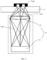
- FIG. 4 shows an internal structure of a second fingerprint apparatus 05 in the prior art.
- the fingerprint apparatus 05 is installed below a screen 01, and includes an image sensor 051 and a lens structure 053 located between the image sensor 051 and the screen 01.
- fingerprint information light of the finger passes through the screen 01, is focused by the lens structure 053 for reverse imaging, and then is transmitted to the image sensor 051.
- the image sensor 051 may recognize fingerprint information.
- FIG. 5 is a schematic structural diagram in which the fingerprint apparatus 05 in this solution is installed in an electronic device architecture.
- the lens structure 053 is disposed in the fingerprint apparatus 05 in this solution to fit with the image sensor 051, and therefore a specific distance is required for optical path propagation of the fingerprint apparatus 05 to ensure reverse imaging, that is, the fingerprint apparatus 05 is relatively thick. Therefore the fingerprint apparatus 05 can be installed only in a non-battery region 04.
- the fingerprint apparatus 100 is disposed below a display screen 200 of an electronic device, and includes a fingerprint image sensor 101, and further includes a collimator 102 disposed between the fingerprint image sensor 101 and the display screen 200.
- a first microlens group 103 is disposed between the collimator 102 and the display screen 200.
- the first microlens group 103 includes at least one first microlens unit 1031.
- the first microlens unit 1031 corresponds to a collimator hole 1021 of the collimator 102, and is disposed above the collimator 102.
- the first microlens unit 1031 is configured to converge fingerprint image light information above the display screen 200 to the collimator hole 1021 of the collimator 102.
- the first microlens group 103 is disposed on a side of the collimator 102 that is away from the fingerprint image sensor 101, the first microlens group 103 includes at least one first microlens unit 1031, and the first microlens unit 1031 is disposed corresponding to the collimator hole 1021 of the collimator 102.
- the fingerprint apparatus 100 may be installed at another position without being attached to the screen.
- An installation position is flexible, and therefore a problem that the screen is scrapped due to installation of the fingerprint apparatus through attachment to the screen can be avoided.
- a microlens structure with a relatively small size is used to integrate light, which is different from a reflection imaging solution of a convex lens with a relatively large size of a camera in the solution shown in FIG. 4 . Therefore, the entire fingerprint apparatus 100 is relatively thin, and may be flexibly installed at a plurality of positions in small space.
- the collimator may be made of a material such as a silicon material, glass fiber, or plastic.
- the collimator is disposed on a surface on a side of the fingerprint sensor, and may be used to block incident light at an angle, to a surface of the fingerprint sensor, that exceeds a specific angle threshold, to ensure that incident light perpendicular to or approximately perpendicular to the surface of the fingerprint sensor is incident on the surface of the fingerprint sensor, so as to improve light utilization and reduce interference from stray light.
- the fingerprint apparatus 100 when the fingerprint apparatus 100 provided in this embodiment of this application is relatively far away from the display screen 200, the fingerprint apparatus 100 can still normally recognize fingerprint information, and may not need to be attached to the display screen 200 for installation in this case.
- An installation position is flexible, and therefore a problem that the screen is scrapped due to installation of the fingerprint apparatus through attachment to the screen can be avoided.
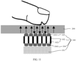
- a second microlens group 104 is further disposed between the collimator hole 1021 and the fingerprint image sensor 101.
- the second microlens group 104 includes at least one second microlens unit 1041.
- the second microlens unit 1041 is disposed corresponding to the collimator hole 1021 of the collimator 102.
- the second microlens unit 1041 is configured to converge light that passes through the collimator hole 1021 of the collimator 102 to the fingerprint image sensor 101.
- the first microlens group 103 may converge light that cannot be incident into the collimator hole 1021 or that cannot be transmitted in a straight line into the collimator hole 1021, thereby increasing light transmittance.
- the second microlens group 104 may converge the light that passes through the collimator hole 1021 to the fingerprint image sensor 101, thereby improving a fingerprint recognition effect.
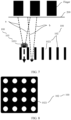
- the collimator 102 includes a plurality of collimator holes 1021.
- the plurality of first microlens units 1031 are disposed in a one-to-one correspondence with the plurality of collimator holes 1021 of the collimator 102.
- each collimator hole 1021 there may be a plurality of second microlens units 1041.
- FIG. 11 there are a plurality of second microlens units 1041, and the plurality of second microlens units 1041 are disposed in a one-to-one correspondence with the plurality of collimator holes 1021 of the collimator 102.
- the first microlens unit 1031 is a convex lens with a light convergence function, and a specific shape and structure of the convex lens may be flexibly adjusted based on an actual optical path requirement and an assembly requirement. As shown in FIG. 6 , a side, of the convex lens, that faces the collimator hole is relatively flat to facilitate assembly.
- the convex lenses namely, the first microlens unit 1031 and the second microlens unit 1041 herein, are disposed corresponding to the collimator hole 1021 of the collimator 102, and are different from the lens structure 053 in the prior art shown in FIG. 4 .
- the first microlens unit 1031 and the second microlens unit 1041 are smaller in size, and are used only to integrate light. Therefore, less impact is exerted on a thickness of the entire fingerprint apparatus 100.
- the fingerprint apparatus 100 To supply power and transmit a signal to the fingerprint image sensor 101, a corresponding connection structure circuit is usually required, for example, a wire, a signal cable, or a printed circuit board.
- the fingerprint apparatus 100 further includes a flexible circuit board 105 configured to transmit a current and a signal.
- the fingerprint image sensor 101 is fastened on the flexible circuit board 105.
- the flexible circuit board 105 may have a relatively large deformation rate, to facilitate assembly on the premise of ensuring power supply and signal transmission.
- an embodiment of this application further provides an electronic device.
- the electronic device includes a display screen 200.
- the fingerprint apparatus 100 according to any one of the foregoing technical solutions is disposed at an interval below the display screen 200.
- the fingerprint apparatus 100 and the display screen 200 are usually disposed at an interval during assembly and installation. After testing and calculation, a gap between the display screen 200 and the fingerprint apparatus 100 may be greater than or equal to 0.1 mm.
- the fingerprint apparatus 100 is fastened to the middle frame 300 through attachment and bonding.
- the display screen 200 is usually located in an upward direction, to facilitate operation for a user. Therefore, two directions, namely, the upward direction and a downward direction, are determined. Specifically, referring to FIG. 13 and FIG. 14 , in a thickness direction of the electronic device, a direction from the middle frame 300 to the display screen 200 is the upward direction, and a direction from the display screen 200 to the middle frame 300 is the downward direction.
- the display screen 200 includes a light emitting surface and a backlight surface. The light emitting surface may display an image, and the backlight surface is opposite to the light emitting surface. A side close to the backlight surface is below the display screen.
- the fingerprint apparatus 100 and the display screen 200 are disposed at an interval.
- a side edge of the middle frame 300 or another intermediate structure (for example, a plastic frame) is usually connected to a side edge of the display screen 200, to fasten the display screen 200. Therefore, a specific safety gap also needs to be ensured between the middle frame 300 and the display region of the display screen 200.
- the gap is also greater than or equal to 0.1 mm.
- the fingerprint apparatus 100 is smaller in size relative to the middle frame 300, and is installed on the middle frame 300, and then the middle frame 300 is assembled with the display screen 200.
- a distance between the middle frame 300 and the display screen 200 is a reference standard during installation.
- FIG. 13 provided that it is ensured that an upper surface of the middle frame 300 is higher than an upper surface of the fingerprint apparatus 100, it can be ensured, by considering only the distance between the middle frame 300 and the display screen 200 during installation, that there is a sufficient gap between the display screen 200 and each of the middle frame 300 and the fingerprint apparatus 100.
- a groove 301 is disposed downward at a position, on the upper surface of the middle frame 300, corresponding to the fingerprint apparatus 100. The fingerprint apparatus 100 is fastened in the groove 301.
- the middle frame 300 includes a middle frame body 302 and a middle frame support member 303.
- the groove 301 is disposed on the middle frame support member 303.
- a mounting hole 304 is disposed on the middle frame body 302.
- the middle frame support member 303 is disposed in the mounting hole 304.
- the mounting hole 304 is a stepped hole disposed downward along the middle frame body 302, and an outer profile of a lower surface of the middle frame support member 303 matches the stepped hole. Fitting with the stepped hole may play a limiting role to prevent the middle frame support member 303 from falling from the mounting hole 304.
- the electronic device in this embodiment of this application includes a battery module 400 disposed below the middle frame 300.
- the battery module 400 is disposed in the battery region 500.
- the fingerprint apparatus 100 is located above the battery region 500, or the fingerprint apparatus 100 is located above the non-battery region 600, or the fingerprint apparatus 100 is located above the battery region 500 and the non-battery region.
- That the fingerprint apparatus is disposed above the battery region 500 may be understood as follows: The fingerprint apparatus is located above the non-battery region in the thickness direction of the electronic device, and an orthographic projection of the fingerprint apparatus on the middle frame 300 is located in a region of an orthographic projection of the battery region 500 on the middle frame 300.
- that the fingerprint apparatus is disposed above the non-battery region 600 may be understood as follows: The fingerprint apparatus is located above the non-battery region in the thickness direction of the electronic device, and an orthographic projection of the fingerprint apparatus on the middle frame 300 is located in a region of an orthographic projection of the non-battery region 600 on the middle frame 300.
- the fingerprint apparatus is disposed above the battery region 500 and the non-battery region 600 may be understood as follows:
- the fingerprint apparatus is located above the battery region 500 and the non-battery region 600 in the thickness direction of the electronic device, and an orthographic projection of the fingerprint apparatus on the middle frame 300 is located in a region of an orthographic projection of the battery region on the middle frame 300 and a region of an orthographic projection of the non-battery region on the middle frame 300.
- a bottom surface of the fingerprint apparatus 100 is fastened to a bottom surface of the groove 301 through attachment.
- a side wall of the groove 301 from damaging the fingerprint apparatus 100 in an installation process, there is an avoidance gap between a side wall of the fingerprint apparatus 100 and the side wall of the groove 301.
- the avoidance gap is greater than or equal to 0.3 mm.
- the middle frame body 302 and the middle frame support member 303 may fit with each other in a manner of using the mounting hole 304 in the foregoing solution.
- a manner of slotting the middle frame body 302 is used.
- the fingerprint apparatus 100 is located in a slot, that is, the middle frame body 302 is not penetrated through by the slot.
- the middle frame body 302 there is a slotting manner for receiving a structure of the fingerprint apparatus 100.
- the middle frame 300 includes the middle frame body 302 and the middle frame support member 303.
- the groove 301 is disposed on the middle frame support member 303, an assembly slot is disposed on the middle frame body 302, and the middle frame support member 303 is disposed in the assembly slot.
- the middle frame body 302 may be punctured, and a peripheral wall of the fingerprint apparatus 100 is fastened to a side wall of a hole through attachment.
- the thickness of the electronic device may be reduced.
- middle frame body 302 is usually made of an aluminum alloy material
- the middle frame support member 303 may be made of any one of an aluminum alloy material, a steel sheet, an FR4 resin material whose strength meets a requirement, or the like.
- an embodiment of this application further provides a manufacturing method.
- the method is used to manufacture the electronic device according to any one of the foregoing technical solutions, and includes the following steps:
- the manufacturing method provided in this embodiment of this application is used to manufacture the electronic device according to any one of the foregoing technical solutions.
- the fingerprint apparatus 100 is fastened to the middle frame 300, and therefore a problem that the screen is scrapped due to installation of the fingerprint apparatus through attachment to the screen can be avoided.
- the electronic device when the electronic device includes a battery module 400 disposed below the middle frame 300, there are a battery region 500 and a non-battery region 600 below the middle frame 300.
- the battery module 400 is disposed in the battery region 500.
- the fastening a fingerprint apparatus 100 to a middle frame 300 includes:
- the fingerprint apparatus 100 is fastened to the middle frame 300, and the middle frame 300 includes a middle frame body 302 and a middle frame support member 303. In this way, the fingerprint apparatus 100 may be fastened to the middle frame 300 in different assembly sequences.
- the fastening a fingerprint apparatus 100 to a middle frame 300 includes:
- the middle frame support member 303 In the solution in which the middle frame body 302, the middle frame support member 303, and the fingerprint apparatus 100 are separately and sequentially assembled and fastened, the fingerprint apparatus 100, the middle frame support member 303, and the middle frame body 302 are independent of each other, and the fingerprint apparatus 100, the middle frame support member 303, and the middle frame body 302 need to be sequentially assembled.
- the middle frame support member 303 may be made of a same material as the middle frame body 303, for example, a stainless steel material.
- a specific shape may be formed through stamping or CNC (Computerized Numerical Control, computer numerical control) processing based on a process requirement.
- CNC Computerized Numerical Control
- the middle frame support member 303 and the fingerprint apparatus 100 are assembled as a whole, and then the middle frame body 302 is fastened to the middle frame support member 303, the fingerprint apparatus 100 and the middle frame support member 303 are combined as an integrated component.
- the fingerprint apparatus 100 and the middle frame support member 303 are first assembled into an integrated component, and then are directly assembled with the paired middle frame body 302.
- the middle frame support member 303 may be used as a steel stiffener of the fingerprint apparatus 100, and may be pressed with the fingerprint apparatus 100 to form an integrated component, and then the display screen 200 is assembled.
- process and assembly steps are reduced, and module reliability is improved by using the middle frame support member 303.
- the middle frame body 302 and the middle frame support member 303 are assembled as a whole, and then the fingerprint apparatus 100 is fastened to the middle frame support member 303, the middle frame support member 303 and the middle frame body 302 are combined as an integrated incoming material, the middle frame body 302 may be partially etched or stamped in a fingerprint attachment region to reduce a thickness, then the fingerprint apparatus 100 is directly attached to the integrated middle frame 300 for assembly, and finally the display screen 200 is assembled. In this solution, process and assembly steps are also reduced, but it is relatively difficult to process the middle frame 300.
Landscapes
- Physics & Mathematics (AREA)
- Engineering & Computer Science (AREA)
- General Physics & Mathematics (AREA)
- Optics & Photonics (AREA)
- Human Computer Interaction (AREA)
- Multimedia (AREA)
- Theoretical Computer Science (AREA)
- Image Input (AREA)
- Devices For Indicating Variable Information By Combining Individual Elements (AREA)
Description
- This application relates to the field of electronic device technologies, and in particular, to a fingerprint apparatus, an electronic device, and a manufacturing method thereof.
- With development of science and technology, an electronic device has been basically popularized in all aspects of people's living environment. To make it more convenient for the electronic device to serve people, information exchange between the electronic device and people is crucial. An electronic device such as a mobile phone is used as an example. Information exchange between the mobile phone and a human mainly includes keyboard pressing, screen touching, wireless communication, voice input, facial recognition, fingerprint recognition, and the like. Fingerprint recognition has been widely used in operations such as unlocking and payment in the mobile phone for uniqueness and convenience.
- The mobile phone is used as an example. An existing fingerprint recognition system is usually disposed at a position at which a front physical button is located, disposed on a back, and disposed below a display screen. Nowadays, full-screen display is an important development direction and a technical selling point for future electronic devices such as a mobile phone, and an in-screen fingerprint recognition technology corresponding to full-screen display can draw more attention for user-friendliness. Currently, common in-screen fingerprint recognition technologies include an optical fingerprint recognition technology, a capacitive fingerprint recognition technology, an ultrasonic fingerprint recognition technology, and the like. To improve competitiveness of electronic devices such as the mobile phone, impact of a fingerprint apparatus on architecture design of the electronic devices such as the mobile phone needs to be minimized, and more attention needs to be paid on impact of a location of the fingerprint apparatus in the electronic device and a thickness and an area of the fingerprint apparatus on the architecture design. An existing fingerprint apparatus cannot receive a fingerprint image at a relatively long distance, and therefore usually needs to be installed through attachment to a screen. It is relatively difficult to implement installation through attachment to the screen, and there is a problem that the display screen is scrapped due to poor attachment.
CN 109 791 612 A discloses a fingerprint identification device which includes a micro- telecentric lens array group, for receiving optical signal reflected from a human finger and a fingerprint sensor set to the lower section of micro- telecentric lens array group.CN 208 848 221 U discloses an optical fingerprint identification device able that includes a light detection array, a first shading layer formed above the light detection array, wherein the first shading layer is provided with multiple light passing apertures, a first microlens array set to above first shading layer, wherein the first microlens array is used to converge optical signal to the multiple light passing apertures of the first shading layer, and the optical signal is transmitted to the light detection array by the multiple light passing apertures of the first shading layer.CN 109 791 610 A discloses a fingerprint identification device, to be applied on a electronic equipment, which includes a support plate, at least one fingerprint sensor chip set to the upper surface of the support plate, wherein the support plate is used to be mounted on the center of the electronic equipment. - The present invention is defined by the appended claims.
- An installation position is flexible, and therefore a problem that a screen is scrapped due to installation of the fingerprint apparatus through attachment to the screen can be avoided.
-
-
FIG. 1 is a schematic stacking diagram of an architecture of an existing electronic device; -
FIG. 2 is a schematic structural diagram of a first fingerprint apparatus in the prior art; -
FIG. 3 is a schematic structural diagram in which a first fingerprint apparatus in the prior art is installed in an electronic device; -
FIG. 4 is a schematic structural diagram of a second fingerprint apparatus in the prior art; -
FIG. 5 is a schematic structural diagram in which a second fingerprint apparatus in the prior art is installed in an electronic device; -
FIG. 6 is a schematic structural diagram of a fingerprint apparatus according to an embodiment of this application; -
FIG. 7 is a schematic structural diagram of detecting fingerprint information by a fingerprint apparatus according to an embodiment of this application; -
FIG. 8 is a schematic structural diagram of a collimator of a fingerprint apparatus according to an embodiment of this application; -
FIG. 9 is a schematic structural diagram in which no first microlens unit is disposed for a collimator hole of a fingerprint apparatus according to an embodiment of this application; -
FIG. 10 is a schematic structural diagram in which a first microlens unit is disposed for a collimator hole of a fingerprint apparatus according to an embodiment of this application; -
FIG. 11 is a schematic structural diagram in which a second microlens unit is disposed in a fingerprint apparatus according to an embodiment of this application; -
FIG. 12 is a schematic structural diagram in which a fingerprint apparatus includes a flexible circuit board according to an embodiment of this application; -
FIG. 13 is a schematic cross-sectional structural diagram of an electronic device according to an embodiment of this application; and -
FIG. 14 is an exploded diagram in which a display screen, a fingerprint apparatus, and a middle frame of an electronic device are installed through fitting according to an embodiment of this application. - 01: Screen; 02: Fastening frame; 03: Battery region; 04: Non-battery region; 05: Fingerprint apparatus; 051: Image sensor; 052: Collimation component; 053: Lens structure; 100: Fingerprint apparatus; 101: Fingerprint image sensor; 102: Collimator; 1021: Collimator hole; 103: First microlens group; 1031: First microlens unit; 104: Second microlens group; 1041: Second microlens unit; 105: Flexible circuit board; 200: Display screen; 300: Middle frame; 301: Groove; 302: Middle frame body; 303: Middle frame support member; 304: Mounting hole; 400: Battery module; 500: Battery region; and 600: Non-battery region.
- To facilitate understanding of the solutions, related structure stacking related to installation of a fingerprint apparatus in an electronic device is briefly described herein.
FIG. 1 is a schematic stacking diagram of a typical architecture of an existing electronic device such as a mobile phone. The architecture includes ascreen 01 and afastening frame 02. Space below the fasteningframe 02 may be divided into abattery region 03 and anon-battery region 04 based on different disposed parts. Thebattery region 03 is used to accommodate a power supply. Thenon-battery region 04 is used to accommodate other optional electronic elements such as a circuit board, a speaker box, a motor, and a camera. Based on the architecture, a fingerprint apparatus is placed below thescreen 01. The fingerprint apparatus may be fastened to thescreen 01 or thefastening frame 02. In addition, the fingerprint apparatus may be located above thebattery region 03 or thenon-battery region 04. Due to a limitation of a structure or the prior art, in the foregoing solution of positions for disposing the fingerprint apparatus, there is a possibility that the fingerprint apparatus cannot be disposed at some of the positions, or there may be some problems after implementation. For example, when the fingerprint apparatus is attached to thescreen 01 for assembly, there is a problem of relatively high costs due to poor attachment, and a limited thickness of the fingerprint apparatus affects a battery capacity or results in an increase in a thickness of the entire device. When the fingerprint apparatus is relatively thick, the fingerprint apparatus can be disposed only above thenon-battery region 04. However, a requirement for a large-area in-screen fingerprint cannot be met due to a limited area of thenon-battery region 04. In a thickness direction of the electronic device, a direction from the fastening frame to the screen is an upward direction, and a direction from the screen to the fastening frame is a downward direction. The fingerprint apparatus may be located above thebattery region 03. It may be understood that the fingerprint apparatus is located above the battery region in the thickness direction of the electronic device, and an orthographic projection of the fingerprint apparatus on the fastening frame is located in a region of an orthographic projection of the battery region on the fastening frame. Correspondingly, the fingerprint apparatus may be located above thenon-battery region 04. It may be understood that the fingerprint apparatus is located above the non-battery region in the thickness direction of the electronic device, and an orthographic projection of the fingerprint apparatus on the fastening frame is located in a region of an orthographic projection of the battery region on the fastening frame. - For example, there are usually the following two implementations for an in-screen fingerprint in the prior art:
FIG. 2 shows an internal structure of afirst fingerprint apparatus 05 in the prior art. Thefingerprint apparatus 05 is installed below ascreen 01, and includes animage sensor 051 and acollimation component 052. When a human finger presses thescreen 01, fingerprint information light of the finger passes through thescreen 01, is integrated by thecollimation component 052, and then is transmitted to theimage sensor 051. Theimage sensor 051 may recognize fingerprint information.FIG. 3 is a schematic structural diagram in which thefingerprint apparatus 05 in this solution is installed in an electronic device architecture. Only thecollimation component 052 with a relatively small size is disposed in thefingerprint apparatus 05 in this solution to fit with theimage sensor 051, and therefore thefingerprint apparatus 05 is relatively thin, and may be installed in abattery region 03 or anon-battery region 04. However, in a solution of attaching thefingerprint apparatus 05 to thescreen 01, there is a problem that thescreen 01 is scrapped due to poor attachment. In addition, if thecollimation component 052 of thefingerprint apparatus 05 in this solution is relatively far away from thescreen 01, there is relatively low light transmittance, an optical fingerprint image is distorted, and recognition cannot be performed well. Consequently, fingerprint information cannot be normally collected, and normal operation is affected. -
FIG. 4 shows an internal structure of asecond fingerprint apparatus 05 in the prior art. Thefingerprint apparatus 05 is installed below ascreen 01, and includes animage sensor 051 and alens structure 053 located between theimage sensor 051 and thescreen 01. When a human finger presses thescreen 01, fingerprint information light of the finger passes through thescreen 01, is focused by thelens structure 053 for reverse imaging, and then is transmitted to theimage sensor 051. Theimage sensor 051 may recognize fingerprint information.FIG. 5 is a schematic structural diagram in which thefingerprint apparatus 05 in this solution is installed in an electronic device architecture. Thelens structure 053 is disposed in thefingerprint apparatus 05 in this solution to fit with theimage sensor 051, and therefore a specific distance is required for optical path propagation of thefingerprint apparatus 05 to ensure reverse imaging, that is, thefingerprint apparatus 05 is relatively thick. Therefore thefingerprint apparatus 05 can be installed only in anon-battery region 04. - An embodiment of this application provides a
fingerprint apparatus 100. Referring toFIG. 6 , thefingerprint apparatus 100 is disposed below adisplay screen 200 of an electronic device, and includes afingerprint image sensor 101, and further includes acollimator 102 disposed between thefingerprint image sensor 101 and thedisplay screen 200. Afirst microlens group 103 is disposed between thecollimator 102 and thedisplay screen 200. Thefirst microlens group 103 includes at least onefirst microlens unit 1031. Thefirst microlens unit 1031 corresponds to acollimator hole 1021 of thecollimator 102, and is disposed above thecollimator 102. Thefirst microlens unit 1031 is configured to converge fingerprint image light information above thedisplay screen 200 to thecollimator hole 1021 of thecollimator 102. - In the
fingerprint apparatus 100 provided in this embodiment of this application, referring toFIG. 6 , thefirst microlens group 103 is disposed on a side of thecollimator 102 that is away from thefingerprint image sensor 101, thefirst microlens group 103 includes at least onefirst microlens unit 1031, and thefirst microlens unit 1031 is disposed corresponding to thecollimator hole 1021 of thecollimator 102. In this way, when thefingerprint apparatus 100 is relatively far away from thedisplay screen 200, the fingerprint image light information can still be smoothly transmitted to thefingerprint image sensor 101, thereby removing a limitation that thefingerprint apparatus 100 can be installed only through attachment to the screen. In addition, thefingerprint apparatus 100 may be installed at another position without being attached to the screen. An installation position is flexible, and therefore a problem that the screen is scrapped due to installation of the fingerprint apparatus through attachment to the screen can be avoided. In addition, a microlens structure with a relatively small size is used to integrate light, which is different from a reflection imaging solution of a convex lens with a relatively large size of a camera in the solution shown inFIG. 4 . Therefore, theentire fingerprint apparatus 100 is relatively thin, and may be flexibly installed at a plurality of positions in small space. - It should be noted that the collimator (collimator) may be made of a material such as a silicon material, glass fiber, or plastic. The collimator is disposed on a surface on a side of the fingerprint sensor, and may be used to block incident light at an angle, to a surface of the fingerprint sensor, that exceeds a specific angle threshold, to ensure that incident light perpendicular to or approximately perpendicular to the surface of the fingerprint sensor is incident on the surface of the fingerprint sensor, so as to improve light utilization and reduce interference from stray light.
- To clearly describe an effect of the
fingerprint apparatus 100 provided in this embodiment of this application, referring toFIG. 7 , when a finger presses thedisplay screen 200, fingerprint light information is transmitted downward through thecollimator hole 1021. A structure of thecollimator hole 1021 disposed on thecollimator 102 is shown inFIG. 8 . For example, further referring toFIG. 7 , the fingerprint light information includes light a and light b in the figure. Thefirst microlens unit 1031 is disposed for acollimator hole 1021 to which the light a points, and nofirst microlens unit 1031 is disposed for acollimator hole 1021 to which the light b points. In this case, the light a is transmitted more efficiently than the light b. Specifically, referring toFIG. 9 , when nofirst microlens unit 1031 is disposed above thecollimator hole 1021, in four beams of light e, f, g, and h shown in the figure, light in a range of f and g can be smoothly transmitted from one side of thecollimator hole 1021 to the other side, and light outside the range of f and g, for example, the light e and h, cannot be correctly transmitted from one side of thecollimator hole 1021 to the other side. In comparison withFIG. 9 , referring toFIG. 10 , when thefirst microlens unit 1031 is disposed corresponding to thecollimator hole 1021, light (including light f and g) in a range of light e and h is refracted and integrated by thefirst microlens unit 1031, and can be smoothly transmitted from one side of thecollimator hole 1021 to the other side. It may be clearly learned that in comparison with a fingerprint apparatus in which nofirst microlens unit 1031 is disposed, in thefingerprint apparatus 100 in which thefirst microlens unit 1031 is disposed, light transmittance is clearly improved. Therefore, when thefingerprint apparatus 100 provided in this embodiment of this application is relatively far away from thedisplay screen 200, thefingerprint apparatus 100 can still normally recognize fingerprint information, and may not need to be attached to thedisplay screen 200 for installation in this case. An installation position is flexible, and therefore a problem that the screen is scrapped due to installation of the fingerprint apparatus through attachment to the screen can be avoided. - To implement better transmission and imaging of light emitted from the
collimator hole 1021, asecond microlens group 104 is further disposed between thecollimator hole 1021 and thefingerprint image sensor 101. As shown inFIG. 11 , thesecond microlens group 104 includes at least onesecond microlens unit 1041. Thesecond microlens unit 1041 is disposed corresponding to thecollimator hole 1021 of thecollimator 102. Thesecond microlens unit 1041 is configured to converge light that passes through thecollimator hole 1021 of thecollimator 102 to thefingerprint image sensor 101. Thefirst microlens group 103 may converge light that cannot be incident into thecollimator hole 1021 or that cannot be transmitted in a straight line into thecollimator hole 1021, thereby increasing light transmittance. Thesecond microlens group 104 may converge the light that passes through thecollimator hole 1021 to thefingerprint image sensor 101, thereby improving a fingerprint recognition effect. - Referring to
FIG. 8 , thecollimator 102 includes a plurality of collimator holes 1021. To increase light transmittance of eachcollimator hole 1021, there may be a plurality offirst microlens units 1031. Specifically, as shown inFIG. 6 , there are a plurality offirst microlens units 1031, and the plurality offirst microlens units 1031 are disposed in a one-to-one correspondence with the plurality ofcollimator holes 1021 of thecollimator 102. - Similarly, to further converge fingerprint image light information that passes through each
collimator hole 1021 to the fingerprint image sensor, there may be a plurality ofsecond microlens units 1041. As shown inFIG. 11 , there are a plurality ofsecond microlens units 1041, and the plurality ofsecond microlens units 1041 are disposed in a one-to-one correspondence with the plurality ofcollimator holes 1021 of thecollimator 102. - The
first microlens unit 1031 is a convex lens with a light convergence function, and a specific shape and structure of the convex lens may be flexibly adjusted based on an actual optical path requirement and an assembly requirement. As shown inFIG. 6 , a side, of the convex lens, that faces the collimator hole is relatively flat to facilitate assembly. - Similarly, the
second microlens unit 1041 is a convex lens. Thesecond microlens unit 1041 is a convex lens with a light convergence function, and a specific shape and structure of the convex lens may be flexibly adjusted based on an actual optical path requirement and an assembly requirement. As shown inFIG. 11 , a side, of the convex lens, that faces the collimator hole is relatively flat to facilitate assembly. - It should be noted that referring to
FIG. 12 , the convex lenses, namely, thefirst microlens unit 1031 and thesecond microlens unit 1041 herein, are disposed corresponding to thecollimator hole 1021 of thecollimator 102, and are different from thelens structure 053 in the prior art shown inFIG. 4 . In comparison with thelens structure 053 for implementing reverse imaging through light focusing inFIG. 4 , thefirst microlens unit 1031 and thesecond microlens unit 1041 are smaller in size, and are used only to integrate light. Therefore, less impact is exerted on a thickness of theentire fingerprint apparatus 100. - To supply power and transmit a signal to the
fingerprint image sensor 101, a corresponding connection structure circuit is usually required, for example, a wire, a signal cable, or a printed circuit board. To facilitate installation and assembly, as shown inFIG. 12 , thefingerprint apparatus 100 further includes aflexible circuit board 105 configured to transmit a current and a signal. Thefingerprint image sensor 101 is fastened on theflexible circuit board 105. Theflexible circuit board 105 may have a relatively large deformation rate, to facilitate assembly on the premise of ensuring power supply and signal transmission. - According to a second aspect, an embodiment of this application further provides an electronic device. As shown in
FIG. 13 , the electronic device includes adisplay screen 200. Thefingerprint apparatus 100 according to any one of the foregoing technical solutions is disposed at an interval below thedisplay screen 200. - As shown in
FIG. 13 , the electronic device provided in this embodiment of this application includes thedisplay screen 200. Thefingerprint apparatus 100 according to any one of the foregoing technical solutions is disposed at an interval below thedisplay screen 200, and therefore thefingerprint apparatus 100 is not attached to thedisplay screen 200. In this way, a problem that the screen is scrapped due to installation of the fingerprint apparatus through attachment to the screen can be avoided. - To prevent the
fingerprint apparatus 100 from coming into contact with thedisplay screen 200 to damage thedisplay screen 200, thefingerprint apparatus 100 and thedisplay screen 200 are usually disposed at an interval during assembly and installation. After testing and calculation, a gap between thedisplay screen 200 and thefingerprint apparatus 100 may be greater than or equal to 0.1 mm. - A corresponding installation support structure such as a middle frame is usually required for fastening the
display screen 200 and a plurality of other parts of the electronic device. Therefore, as shown inFIG. 13 , the electronic device in this embodiment of this application includes amiddle frame 300 located below thedisplay screen 200. Thefingerprint apparatus 100 may be fastened to themiddle frame 300. - To facilitate fastening of the
fingerprint apparatus 100 to themiddle frame 300, thefingerprint apparatus 100 is fastened to themiddle frame 300 through attachment and bonding. - It should be noted that in the electronic device in this embodiment of this application, for ease of description, based on a use habit of the electronic device, the
display screen 200 is usually located in an upward direction, to facilitate operation for a user. Therefore, two directions, namely, the upward direction and a downward direction, are determined. Specifically, referring toFIG. 13 andFIG. 14 , in a thickness direction of the electronic device, a direction from themiddle frame 300 to thedisplay screen 200 is the upward direction, and a direction from thedisplay screen 200 to themiddle frame 300 is the downward direction. It may be understood that thedisplay screen 200 includes a light emitting surface and a backlight surface. The light emitting surface may display an image, and the backlight surface is opposite to the light emitting surface. A side close to the backlight surface is below the display screen. - The
fingerprint apparatus 100 may be relatively thin, and therefore may be disposed above a battery region or a non-battery region of the electronic device. When thefingerprint apparatus 100 is located above the battery region of the electronic device, if a lower surface of thefingerprint apparatus 100 is lower than a lower surface of themiddle frame 300, a battery may be punctured, resulting in a serious consequence of burning the entire device. Therefore, to prevent thefingerprint apparatus 100 from puncturing the battery, referring toFIG. 13 , optionally, the lower surface of themiddle frame 300 is lower than the lower surface of thefingerprint apparatus 100. Certainly, if a process error can be ensured, the lower surface of themiddle frame 300 may be coplanar with the lower surface of thefingerprint apparatus 100. - The
fingerprint apparatus 100 and thedisplay screen 200 are disposed at an interval. In addition, during assembly of thedisplay screen 200 and themiddle frame 300, to prevent themiddle frame 300 from squeezing a display region of thedisplay screen 200, a side edge of themiddle frame 300 or another intermediate structure (for example, a plastic frame) is usually connected to a side edge of thedisplay screen 200, to fasten thedisplay screen 200. Therefore, a specific safety gap also needs to be ensured between themiddle frame 300 and the display region of thedisplay screen 200. Optionally, the gap is also greater than or equal to 0.1 mm. Thefingerprint apparatus 100 is smaller in size relative to themiddle frame 300, and is installed on themiddle frame 300, and then themiddle frame 300 is assembled with thedisplay screen 200. In this way, it is not easy to control the gap between thefingerprint apparatus 100 and thedisplay screen 200. Therefore, this can be easily implemented by using a distance between themiddle frame 300 and thedisplay screen 200 as a reference standard during installation. On this basis, as shown inFIG. 13 , provided that it is ensured that an upper surface of themiddle frame 300 is higher than an upper surface of thefingerprint apparatus 100, it can be ensured, by considering only the distance between themiddle frame 300 and thedisplay screen 200 during installation, that there is a sufficient gap between thedisplay screen 200 and each of themiddle frame 300 and the fingerprint apparatus 100.As shown inFIG. 13 , to reduce a thickness of the entire electronic device, agroove 301 is disposed downward at a position, on the upper surface of themiddle frame 300, corresponding to thefingerprint apparatus 100. Thefingerprint apparatus 100 is fastened in thegroove 301. - Assembly of a plurality of electrical elements needs to be considered in the
middle frame 300, and therefore a plurality of structures need to be considered in structure design and layout of themiddle frame 300. To facilitate manufacturing of themiddle frame 300, some installation positions are usually reserved, and then adapted installation parts are manufactured separately to install the electrical elements. For example, as shown inFIG. 13 , themiddle frame 300 includes amiddle frame body 302 and a middleframe support member 303. Thegroove 301 is disposed on the middleframe support member 303. A mountinghole 304 is disposed on themiddle frame body 302. The middleframe support member 303 is disposed in the mountinghole 304. - To prevent the middle
frame support member 303 from falling from the mountinghole 304, as shown inFIG. 13 , the mountinghole 304 is a stepped hole disposed downward along themiddle frame body 302, and an outer profile of a lower surface of the middleframe support member 303 matches the stepped hole. Fitting with the stepped hole may play a limiting role to prevent the middleframe support member 303 from falling from the mountinghole 304. - As shown in
FIG. 13 , the electronic device in this embodiment of this application includes abattery module 400 disposed below themiddle frame 300. There are abattery region 500 and anon-battery region 600 below themiddle frame 300. Thebattery module 400 is disposed in thebattery region 500. Thefingerprint apparatus 100 is located above thebattery region 500, or thefingerprint apparatus 100 is located above thenon-battery region 600, or thefingerprint apparatus 100 is located above thebattery region 500 and the non-battery region. - That the fingerprint apparatus is disposed above the
battery region 500 may be understood as follows: The fingerprint apparatus is located above the non-battery region in the thickness direction of the electronic device, and an orthographic projection of the fingerprint apparatus on themiddle frame 300 is located in a region of an orthographic projection of thebattery region 500 on themiddle frame 300. Correspondingly, that the fingerprint apparatus is disposed above thenon-battery region 600 may be understood as follows: The fingerprint apparatus is located above the non-battery region in the thickness direction of the electronic device, and an orthographic projection of the fingerprint apparatus on themiddle frame 300 is located in a region of an orthographic projection of thenon-battery region 600 on themiddle frame 300. Correspondingly, that the fingerprint apparatus is disposed above thebattery region 500 and thenon-battery region 600 may be understood as follows: The fingerprint apparatus is located above thebattery region 500 and thenon-battery region 600 in the thickness direction of the electronic device, and an orthographic projection of the fingerprint apparatus on themiddle frame 300 is located in a region of an orthographic projection of the battery region on themiddle frame 300 and a region of an orthographic projection of the non-battery region on themiddle frame 300. - As shown in
FIG. 13 , a bottom surface of thefingerprint apparatus 100 is fastened to a bottom surface of thegroove 301 through attachment. To prevent a side wall of thegroove 301 from damaging thefingerprint apparatus 100 in an installation process, there is an avoidance gap between a side wall of thefingerprint apparatus 100 and the side wall of thegroove 301. - Optionally, the avoidance gap is greater than or equal to 0.3 mm.
- The
middle frame body 302 and the middleframe support member 303 may fit with each other in a manner of using the mountinghole 304 in the foregoing solution. Certainly, there may be another manner based on a space requirement and a structural requirement. For example, a manner of slotting themiddle frame body 302 is used. In the manner of slotting themiddle frame body 302, thefingerprint apparatus 100 is located in a slot, that is, themiddle frame body 302 is not penetrated through by the slot. For themiddle frame body 302, there is a slotting manner for receiving a structure of thefingerprint apparatus 100. Specifically, themiddle frame 300 includes themiddle frame body 302 and the middleframe support member 303. Thegroove 301 is disposed on the middleframe support member 303, an assembly slot is disposed on themiddle frame body 302, and the middleframe support member 303 is disposed in the assembly slot. Optionally, themiddle frame body 302 may be punctured, and a peripheral wall of thefingerprint apparatus 100 is fastened to a side wall of a hole through attachment. When a thickness of the middle frame body is the same as a thickness of thefingerprint apparatus 100, the thickness of the electronic device may be reduced. - It should be noted that the
middle frame body 302 is usually made of an aluminum alloy material, and the middleframe support member 303 may be made of any one of an aluminum alloy material, a steel sheet, an FR4 resin material whose strength meets a requirement, or the like. - According to a third aspect, an embodiment of this application further provides a manufacturing method. The method is used to manufacture the electronic device according to any one of the foregoing technical solutions, and includes the following steps:
- fastening a
fingerprint apparatus 100 to amiddle frame 300; and - fastening a
display screen 200 to themiddle frame 300, where thedisplay screen 200 is located above thefingerprint apparatus 100. - The manufacturing method provided in this embodiment of this application is used to manufacture the electronic device according to any one of the foregoing technical solutions. The
fingerprint apparatus 100 is fastened to themiddle frame 300, and therefore a problem that the screen is scrapped due to installation of the fingerprint apparatus through attachment to the screen can be avoided. - Referring to
FIG. 13 andFIG. 14 , when the electronic device includes abattery module 400 disposed below themiddle frame 300, there are abattery region 500 and anon-battery region 600 below themiddle frame 300. Thebattery module 400 is disposed in thebattery region 500. The fastening afingerprint apparatus 100 to amiddle frame 300 includes: - installing the
fingerprint apparatus 100 above thebattery region 500, or - installing the
fingerprint apparatus 100 above thenon-battery region 600, or - installing the
fingerprint apparatus 100 above thebattery region 500 and thenon-battery region 600. - Referring to
FIG. 13 andFIG. 14 , thefingerprint apparatus 100 is fastened to themiddle frame 300, and themiddle frame 300 includes amiddle frame body 302 and a middleframe support member 303. In this way, thefingerprint apparatus 100 may be fastened to themiddle frame 300 in different assembly sequences. - The fastening a
fingerprint apparatus 100 to amiddle frame 300 includes: - separately and sequentially assembling and fastening the
middle frame body 302, the middleframe support member 303, and thefingerprint apparatus 100; or - assembling the middle
frame support member 303 and thefingerprint apparatus 100 as a whole, and then fastening themiddle frame body 302 to the middleframe support member 303; or - assembling the
middle frame body 302 and the middleframe support member 303, and then fastening thefingerprint apparatus 100 to the middleframe support member 303. - In the solution in which the
middle frame body 302, the middleframe support member 303, and thefingerprint apparatus 100 are separately and sequentially assembled and fastened, thefingerprint apparatus 100, the middleframe support member 303, and themiddle frame body 302 are independent of each other, and thefingerprint apparatus 100, the middleframe support member 303, and themiddle frame body 302 need to be sequentially assembled. The middleframe support member 303 may be made of a same material as themiddle frame body 303, for example, a stainless steel material. A specific shape may be formed through stamping or CNC (Computerized Numerical Control, computer numerical control) processing based on a process requirement. In this solution, the components are independent and easy to process, but there are many process and assembly steps. - In the solution in which the middle
frame support member 303 and thefingerprint apparatus 100 are assembled as a whole, and then themiddle frame body 302 is fastened to the middleframe support member 303, thefingerprint apparatus 100 and the middleframe support member 303 are combined as an integrated component. In this way, in a manufacturing process procedure, thefingerprint apparatus 100 and the middleframe support member 303 are first assembled into an integrated component, and then are directly assembled with the pairedmiddle frame body 302. The middleframe support member 303 may be used as a steel stiffener of thefingerprint apparatus 100, and may be pressed with thefingerprint apparatus 100 to form an integrated component, and then thedisplay screen 200 is assembled. In this solution, process and assembly steps are reduced, and module reliability is improved by using the middleframe support member 303. - In the solution in which the
middle frame body 302 and the middleframe support member 303 are assembled as a whole, and then thefingerprint apparatus 100 is fastened to the middleframe support member 303, the middleframe support member 303 and themiddle frame body 302 are combined as an integrated incoming material, themiddle frame body 302 may be partially etched or stamped in a fingerprint attachment region to reduce a thickness, then thefingerprint apparatus 100 is directly attached to the integratedmiddle frame 300 for assembly, and finally thedisplay screen 200 is assembled. In this solution, process and assembly steps are also reduced, but it is relatively difficult to process themiddle frame 300. - In the descriptions of this specification, specific features, structures, materials, or characteristics may be combined in a proper manner in any one or more of the embodiments or examples.
Claims (13)
- A fingerprint apparatus, comprising a fingerprint image sensor and a collimator located on a side of the fingerprint image sensor, wherein a first microlens group is disposed on a side of the collimator that is away from the fingerprint image sensor, the first microlens group comprises at least one first microlens unit, the first microlens unit is disposed corresponding to a collimator hole of the collimator, and the first microlens unit is configured to converge light on the side of the collimator that is away from the fingerprint image sensor to the collimator hole of the collimator;wherein a second microlens group is further disposed between the collimator and the fingerprint image sensor, the second microlens group comprises at least one second microlens unit, the second microlens unit is disposed corresponding to the collimator hole of the collimator, and the second microlens unit is configured to converge light that passes through the collimator hole of the collimator to the fingerprint image sensor;wherein the first microlens unit is a convex lens with a light convergence function, the side of the first microlens unit facing the collimator hole being flat;wherein the second microlens unit is a convex lens with a light convergence function, the side of the second microlens unit facing the collimator hole being flat.
- The fingerprint apparatus according to claim 1, wherein there are a plurality of first microlens units, the collimator comprises a plurality of collimator holes, and the plurality of first microlens units are disposed in a one-to-one correspondence with the plurality of collimator holes of the collimator.
- The fingerprint apparatus according to claim 1 or 2, wherein there are a plurality of second microlens units, the collimator comprises a plurality of collimator holes, and the plurality of second microlens units are disposed in a one-to-one correspondence with the plurality of collimator holes of the collimator.
- The fingerprint apparatus according to any one of claims 1 to 3, further comprising a flexible circuit board configured to transmit a current and a signal, wherein the fingerprint image sensor is fastened on the flexible circuit board.
- An electronic device, comprising a display screen, wherein the fingerprint apparatus according to any one of claims 1 to 4 is disposed at an interval below the display screen.
- The electronic device according to claim 5, comprising a middle frame located below the display screen, wherein the fingerprint apparatus is fastened to the middle frame.
- The electronic device according to claim 6, wherein the fingerprint apparatus is fastened to the middle frame through attachment and bonding.
- The electronic device according to claim 6 or 7, wherein a lower surface of the middle frame is lower than a lower surface of the fingerprint apparatus.
- The electronic device according to any one of claims 6 to 8, wherein an upper surface of the middle frame is higher than an upper surface of the fingerprint apparatus.
- The electronic device according to any one of claims 6 to 9, wherein a groove is disposed downward at a position, on the upper surface of the middle frame, corresponding to the fingerprint apparatus, and the fingerprint apparatus is fastened in the groove.
- The electronic device according to claim 10, wherein the middle frame comprises a middle frame body and a middle frame support member, the groove is disposed on the middle frame support member, a mounting hole is disposed on the middle frame body, and the middle frame support member is disposed in the mounting hole.
- The electronic device according to claim 11, wherein the mounting hole is a stepped hole disposed downward along the middle frame body, and an outer profile of a lower surface of the middle frame support member matches the stepped hole.
- The electronic device according to any one of claims 6 to 12, comprising a battery module disposed below the middle frame, wherein there are a battery region and a non-battery region below the middle frame, the battery module is disposed in the battery region, and the fingerprint apparatus is located above the battery region, the fingerprint apparatus is located above the non-battery region, or the fingerprint apparatus is located above the battery region and the non-battery region.
Applications Claiming Priority (2)
| Application Number | Priority Date | Filing Date | Title |
|---|---|---|---|
| CN201910816948.7A CN110674699A (en) | 2019-08-30 | 2019-08-30 | Fingerprint device, electronic equipment and manufacturing method thereof |
| PCT/CN2020/106632 WO2021036703A1 (en) | 2019-08-30 | 2020-08-03 | Fingerprint apparatus, and electronic device and method for manufacturing same |
Publications (3)
| Publication Number | Publication Date |
|---|---|
| EP4020309A1 EP4020309A1 (en) | 2022-06-29 |
| EP4020309A4 EP4020309A4 (en) | 2022-10-19 |
| EP4020309B1 true EP4020309B1 (en) | 2024-10-16 |
Family
ID=69076569
Family Applications (1)
| Application Number | Title | Priority Date | Filing Date |
|---|---|---|---|
| EP20858226.2A Active EP4020309B1 (en) | 2019-08-30 | 2020-08-03 | Fingerprint apparatus, and electronic device and method for manufacturing same |
Country Status (4)
| Country | Link |
|---|---|
| EP (1) | EP4020309B1 (en) |
| CN (1) | CN110674699A (en) |
| ES (1) | ES2996903T3 (en) |
| WO (1) | WO2021036703A1 (en) |
Families Citing this family (3)
| Publication number | Priority date | Publication date | Assignee | Title |
|---|---|---|---|---|
| CN110674699A (en) * | 2019-08-30 | 2020-01-10 | 华为技术有限公司 | Fingerprint device, electronic equipment and manufacturing method thereof |
| CN113076854A (en) * | 2021-03-30 | 2021-07-06 | 武汉华星光电技术有限公司 | Display panel |
| CN114120850A (en) * | 2021-11-22 | 2022-03-01 | 武汉天马微电子有限公司 | Display device |
Family Cites Families (11)
| Publication number | Priority date | Publication date | Assignee | Title |
|---|---|---|---|---|
| KR102836512B1 (en) * | 2017-01-18 | 2025-07-22 | 삼성전자주식회사 | Electronic device having fingerprint verification function |
| US10331939B2 (en) * | 2017-07-06 | 2019-06-25 | Shenzhen GOODIX Technology Co., Ltd. | Multi-layer optical designs of under-screen optical sensor module having spaced optical collimator array and optical sensor array for on-screen fingerprint sensing |
| CN110175492B (en) * | 2018-07-20 | 2022-03-01 | 神盾股份有限公司 | Optical fingerprint sensing device |
| WO2020132974A1 (en) * | 2018-12-26 | 2020-07-02 | 深圳市汇顶科技股份有限公司 | Fingerprint recognition apparatus and electronic device |
| EP3699809A4 (en) * | 2018-12-29 | 2020-11-04 | Shenzhen Goodix Technology Co., Ltd. | Fingerprint identification device and electronic device |
| CN110088768B (en) * | 2019-03-12 | 2022-03-01 | 深圳市汇顶科技股份有限公司 | Fingerprint recognition device and electronic equipment under screen |
| CN209640879U (en) * | 2019-03-20 | 2019-11-15 | 深圳市汇顶科技股份有限公司 | The device and electronic equipment of fingerprint recognition |
| CN209640880U (en) * | 2019-04-10 | 2019-11-15 | 深圳市汇顶科技股份有限公司 | Optical fingerprint identification devices and electronic equipment |
| CN109903681B (en) * | 2019-04-25 | 2021-09-21 | 京东方科技集团股份有限公司 | Support structure, display device, method of manufacturing the support structure, and method of assembling the display device |
| CN110059655A (en) * | 2019-04-25 | 2019-07-26 | Oppo广东移动通信有限公司 | Electronic equipment |
| CN110674699A (en) * | 2019-08-30 | 2020-01-10 | 华为技术有限公司 | Fingerprint device, electronic equipment and manufacturing method thereof |
-
2019
- 2019-08-30 CN CN201910816948.7A patent/CN110674699A/en active Pending
-
2020
- 2020-08-03 EP EP20858226.2A patent/EP4020309B1/en active Active
- 2020-08-03 ES ES20858226T patent/ES2996903T3/en active Active
- 2020-08-03 WO PCT/CN2020/106632 patent/WO2021036703A1/en not_active Ceased
Also Published As
| Publication number | Publication date |
|---|---|
| CN110674699A (en) | 2020-01-10 |
| ES2996903T3 (en) | 2025-02-13 |
| WO2021036703A1 (en) | 2021-03-04 |
| EP4020309A4 (en) | 2022-10-19 |
| EP4020309A1 (en) | 2022-06-29 |
Similar Documents
| Publication | Publication Date | Title |
|---|---|---|
| CN209895353U (en) | Fingerprint identification devices and electronic equipment | |
| EP3786834B1 (en) | Fingerprint recognition device and electronic apparatus | |
| CN212135453U (en) | Fingerprint detection device and electronic equipment | |
| US11232317B2 (en) | Fingerprint identification apparatus and electronic device | |
| EP3480732B1 (en) | Under-screen biometric identification apparatus, biometric identification assembly, and terminal device | |
| US12335422B2 (en) | Handheld electronic device | |
| EP4020309B1 (en) | Fingerprint apparatus, and electronic device and method for manufacturing same | |
| WO2020118631A1 (en) | Fingerprint recognition apparatus and electronic device | |
| EP3623921A1 (en) | Under-screen biometric recognition apparatus and electronic device | |
| EP3598723B1 (en) | Terminal with casing for a fingerprint recognition unit and flexible display screen | |
| KR20210057702A (en) | Optical fingerprint devices and electronic devices | |
| US12445706B2 (en) | Handheld electronic device with rear-facing flash | |
| US20230224391A1 (en) | Handheld electronic device | |
| CN110709860A (en) | Fingerprint identification device and electronic equipment | |
| CN111801685B (en) | Fingerprint detection device and electronic equipment | |
| US20230224392A1 (en) | Handheld electronic device | |
| CN210864764U (en) | Fingerprint identification device and electronic equipment | |
| CN210864760U (en) | Optical biological characteristic sensing device and mobile phone | |
| CN210864761U (en) | Optical fingerprint sensing device and electronic equipment | |
| WO2022141605A1 (en) | Optical fingerprint detection apparatus and electronic device | |
| CN216014312U (en) | Optical fingerprint identification device and electronic equipment | |
| KR20210138930A (en) | Electronic device including optical sensor module | |
| CN110796122A (en) | Optical fingerprint sensing device and electronic equipment | |
| CN212906320U (en) | Fingerprint identification device and electronic equipment | |
| WO2022141603A1 (en) | Optical fingerprint detection apparatus and electronic device |
Legal Events
| Date | Code | Title | Description |
|---|---|---|---|
| STAA | Information on the status of an ep patent application or granted ep patent |
Free format text: STATUS: THE INTERNATIONAL PUBLICATION HAS BEEN MADE |
|
| PUAI | Public reference made under article 153(3) epc to a published international application that has entered the european phase |
Free format text: ORIGINAL CODE: 0009012 |
|
| STAA | Information on the status of an ep patent application or granted ep patent |
Free format text: STATUS: REQUEST FOR EXAMINATION WAS MADE |
|
| 17P | Request for examination filed |
Effective date: 20220323 |
|
| AK | Designated contracting states |
Kind code of ref document: A1 Designated state(s): AL AT BE BG CH CY CZ DE DK EE ES FI FR GB GR HR HU IE IS IT LI LT LU LV MC MK MT NL NO PL PT RO RS SE SI SK SM TR |
|
| A4 | Supplementary search report drawn up and despatched |
Effective date: 20220916 |
|
| RIC1 | Information provided on ipc code assigned before grant |
Ipc: G02B 13/18 20060101ALI20220912BHEP Ipc: G06V 40/13 20220101AFI20220912BHEP |
|
| DAV | Request for validation of the european patent (deleted) | ||
| DAX | Request for extension of the european patent (deleted) | ||
| REG | Reference to a national code |
Ref country code: DE Ref legal event code: R079 Free format text: PREVIOUS MAIN CLASS: G06K0009000000 Ipc: G06V0040130000 Ref document number: 602020039699 Country of ref document: DE |
|
| GRAP | Despatch of communication of intention to grant a patent |
Free format text: ORIGINAL CODE: EPIDOSNIGR1 |
|
| STAA | Information on the status of an ep patent application or granted ep patent |
Free format text: STATUS: GRANT OF PATENT IS INTENDED |
|
| RIC1 | Information provided on ipc code assigned before grant |
Ipc: G02B 27/30 20060101ALI20240603BHEP Ipc: G02B 3/00 20060101ALI20240603BHEP Ipc: G06V 40/13 20220101AFI20240603BHEP |
|
| INTG | Intention to grant announced |
Effective date: 20240620 |
|
| GRAS | Grant fee paid |
Free format text: ORIGINAL CODE: EPIDOSNIGR3 |
|
| GRAA | (expected) grant |
Free format text: ORIGINAL CODE: 0009210 |
|
| STAA | Information on the status of an ep patent application or granted ep patent |
Free format text: STATUS: THE PATENT HAS BEEN GRANTED |
|
| AK | Designated contracting states |
Kind code of ref document: B1 Designated state(s): AL AT BE BG CH CY CZ DE DK EE ES FI FR GB GR HR HU IE IS IT LI LT LU LV MC MK MT NL NO PL PT RO RS SE SI SK SM TR |
|
| REG | Reference to a national code |
Ref country code: GB Ref legal event code: FG4D |
|
| REG | Reference to a national code |
Ref country code: CH Ref legal event code: EP Ref country code: DE Ref legal event code: R096 Ref document number: 602020039699 Country of ref document: DE |
|
| REG | Reference to a national code |
Ref country code: IE Ref legal event code: FG4D |
|
| REG | Reference to a national code |
Ref country code: LT Ref legal event code: MG9D |
|
| REG | Reference to a national code |
Ref country code: ES Ref legal event code: FG2A Ref document number: 2996903 Country of ref document: ES Kind code of ref document: T3 Effective date: 20250213 |
|
| REG | Reference to a national code |
Ref country code: NL Ref legal event code: MP Effective date: 20241016 |
|
| REG | Reference to a national code |
Ref country code: AT Ref legal event code: MK05 Ref document number: 1733566 Country of ref document: AT Kind code of ref document: T Effective date: 20241016 |
|
| PG25 | Lapsed in a contracting state [announced via postgrant information from national office to epo] |
Ref country code: NL Free format text: LAPSE BECAUSE OF FAILURE TO SUBMIT A TRANSLATION OF THE DESCRIPTION OR TO PAY THE FEE WITHIN THE PRESCRIBED TIME-LIMIT Effective date: 20241016 |
|
| PG25 | Lapsed in a contracting state [announced via postgrant information from national office to epo] |
Ref country code: NL Free format text: LAPSE BECAUSE OF FAILURE TO SUBMIT A TRANSLATION OF THE DESCRIPTION OR TO PAY THE FEE WITHIN THE PRESCRIBED TIME-LIMIT Effective date: 20241016 |
|
| PG25 | Lapsed in a contracting state [announced via postgrant information from national office to epo] |
Ref country code: PT Free format text: LAPSE BECAUSE OF FAILURE TO SUBMIT A TRANSLATION OF THE DESCRIPTION OR TO PAY THE FEE WITHIN THE PRESCRIBED TIME-LIMIT Effective date: 20250217 Ref country code: IS Free format text: LAPSE BECAUSE OF FAILURE TO SUBMIT A TRANSLATION OF THE DESCRIPTION OR TO PAY THE FEE WITHIN THE PRESCRIBED TIME-LIMIT Effective date: 20250216 Ref country code: HR Free format text: LAPSE BECAUSE OF FAILURE TO SUBMIT A TRANSLATION OF THE DESCRIPTION OR TO PAY THE FEE WITHIN THE PRESCRIBED TIME-LIMIT Effective date: 20241016 |
|
| PG25 | Lapsed in a contracting state [announced via postgrant information from national office to epo] |
Ref country code: FI Free format text: LAPSE BECAUSE OF FAILURE TO SUBMIT A TRANSLATION OF THE DESCRIPTION OR TO PAY THE FEE WITHIN THE PRESCRIBED TIME-LIMIT Effective date: 20241016 |
|
| PG25 | Lapsed in a contracting state [announced via postgrant information from national office to epo] |
Ref country code: BG Free format text: LAPSE BECAUSE OF FAILURE TO SUBMIT A TRANSLATION OF THE DESCRIPTION OR TO PAY THE FEE WITHIN THE PRESCRIBED TIME-LIMIT Effective date: 20241016 |
|
| PG25 | Lapsed in a contracting state [announced via postgrant information from national office to epo] |
Ref country code: NO Free format text: LAPSE BECAUSE OF FAILURE TO SUBMIT A TRANSLATION OF THE DESCRIPTION OR TO PAY THE FEE WITHIN THE PRESCRIBED TIME-LIMIT Effective date: 20250116 |
|
| PG25 | Lapsed in a contracting state [announced via postgrant information from national office to epo] |
Ref country code: GR Free format text: LAPSE BECAUSE OF FAILURE TO SUBMIT A TRANSLATION OF THE DESCRIPTION OR TO PAY THE FEE WITHIN THE PRESCRIBED TIME-LIMIT Effective date: 20250117 Ref country code: LV Free format text: LAPSE BECAUSE OF FAILURE TO SUBMIT A TRANSLATION OF THE DESCRIPTION OR TO PAY THE FEE WITHIN THE PRESCRIBED TIME-LIMIT Effective date: 20241016 Ref country code: AT Free format text: LAPSE BECAUSE OF FAILURE TO SUBMIT A TRANSLATION OF THE DESCRIPTION OR TO PAY THE FEE WITHIN THE PRESCRIBED TIME-LIMIT Effective date: 20241016 |
|
| PG25 | Lapsed in a contracting state [announced via postgrant information from national office to epo] |
Ref country code: PL Free format text: LAPSE BECAUSE OF FAILURE TO SUBMIT A TRANSLATION OF THE DESCRIPTION OR TO PAY THE FEE WITHIN THE PRESCRIBED TIME-LIMIT Effective date: 20241016 |
|
| PG25 | Lapsed in a contracting state [announced via postgrant information from national office to epo] |
Ref country code: RS Free format text: LAPSE BECAUSE OF FAILURE TO SUBMIT A TRANSLATION OF THE DESCRIPTION OR TO PAY THE FEE WITHIN THE PRESCRIBED TIME-LIMIT Effective date: 20250116 |
|
| PG25 | Lapsed in a contracting state [announced via postgrant information from national office to epo] |
Ref country code: SM Free format text: LAPSE BECAUSE OF FAILURE TO SUBMIT A TRANSLATION OF THE DESCRIPTION OR TO PAY THE FEE WITHIN THE PRESCRIBED TIME-LIMIT Effective date: 20241016 |
|
| PG25 | Lapsed in a contracting state [announced via postgrant information from national office to epo] |
Ref country code: DK Free format text: LAPSE BECAUSE OF FAILURE TO SUBMIT A TRANSLATION OF THE DESCRIPTION OR TO PAY THE FEE WITHIN THE PRESCRIBED TIME-LIMIT Effective date: 20241016 |
|
| REG | Reference to a national code |
Ref country code: DE Ref legal event code: R097 Ref document number: 602020039699 Country of ref document: DE |
|
| PG25 | Lapsed in a contracting state [announced via postgrant information from national office to epo] |
Ref country code: EE Free format text: LAPSE BECAUSE OF FAILURE TO SUBMIT A TRANSLATION OF THE DESCRIPTION OR TO PAY THE FEE WITHIN THE PRESCRIBED TIME-LIMIT Effective date: 20241016 |
|
| PG25 | Lapsed in a contracting state [announced via postgrant information from national office to epo] |
Ref country code: RO Free format text: LAPSE BECAUSE OF FAILURE TO SUBMIT A TRANSLATION OF THE DESCRIPTION OR TO PAY THE FEE WITHIN THE PRESCRIBED TIME-LIMIT Effective date: 20241016 |
|
| PG25 | Lapsed in a contracting state [announced via postgrant information from national office to epo] |
Ref country code: SK Free format text: LAPSE BECAUSE OF FAILURE TO SUBMIT A TRANSLATION OF THE DESCRIPTION OR TO PAY THE FEE WITHIN THE PRESCRIBED TIME-LIMIT Effective date: 20241016 |
|
| PG25 | Lapsed in a contracting state [announced via postgrant information from national office to epo] |
Ref country code: CZ Free format text: LAPSE BECAUSE OF FAILURE TO SUBMIT A TRANSLATION OF THE DESCRIPTION OR TO PAY THE FEE WITHIN THE PRESCRIBED TIME-LIMIT Effective date: 20241016 |
|
| PLBE | No opposition filed within time limit |
Free format text: ORIGINAL CODE: 0009261 |
|
| STAA | Information on the status of an ep patent application or granted ep patent |
Free format text: STATUS: NO OPPOSITION FILED WITHIN TIME LIMIT |
|
| PG25 | Lapsed in a contracting state [announced via postgrant information from national office to epo] |
Ref country code: SE Free format text: LAPSE BECAUSE OF FAILURE TO SUBMIT A TRANSLATION OF THE DESCRIPTION OR TO PAY THE FEE WITHIN THE PRESCRIBED TIME-LIMIT Effective date: 20241016 |
|
| 26N | No opposition filed |
Effective date: 20250717 |
|
| PGFP | Annual fee paid to national office [announced via postgrant information from national office to epo] |
Ref country code: ES Payment date: 20250905 Year of fee payment: 6 |
|
| PGFP | Annual fee paid to national office [announced via postgrant information from national office to epo] |
Ref country code: DE Payment date: 20250702 Year of fee payment: 6 |
|
| PGFP | Annual fee paid to national office [announced via postgrant information from national office to epo] |
Ref country code: IT Payment date: 20250722 Year of fee payment: 6 |