EP4020229B1 - System, vorrichtung und verfahren zum prefetching von physikalischen seiten in einem prozessor - Google Patents
System, vorrichtung und verfahren zum prefetching von physikalischen seiten in einem prozessor Download PDFInfo
- Publication number
- EP4020229B1 EP4020229B1 EP21198548.6A EP21198548A EP4020229B1 EP 4020229 B1 EP4020229 B1 EP 4020229B1 EP 21198548 A EP21198548 A EP 21198548A EP 4020229 B1 EP4020229 B1 EP 4020229B1
- Authority
- EP
- European Patent Office
- Prior art keywords
- page
- prefetch
- hint
- requests
- processor
- Prior art date
- Legal status (The legal status is an assumption and is not a legal conclusion. Google has not performed a legal analysis and makes no representation as to the accuracy of the status listed.)
- Active
Links
Images


Classifications
-
- G—PHYSICS
- G06—COMPUTING OR CALCULATING; COUNTING
- G06F—ELECTRIC DIGITAL DATA PROCESSING
- G06F9/00—Arrangements for program control, e.g. control units
- G06F9/06—Arrangements for program control, e.g. control units using stored programs, i.e. using an internal store of processing equipment to receive or retain programs
- G06F9/30—Arrangements for executing machine instructions, e.g. instruction decode
- G06F9/38—Concurrent instruction execution, e.g. pipeline or look ahead
- G06F9/3802—Instruction prefetching
-
- G—PHYSICS
- G06—COMPUTING OR CALCULATING; COUNTING
- G06F—ELECTRIC DIGITAL DATA PROCESSING
- G06F12/00—Accessing, addressing or allocating within memory systems or architectures
- G06F12/02—Addressing or allocation; Relocation
- G06F12/08—Addressing or allocation; Relocation in hierarchically structured memory systems, e.g. virtual memory systems
- G06F12/0802—Addressing of a memory level in which the access to the desired data or data block requires associative addressing means, e.g. caches
- G06F12/0862—Addressing of a memory level in which the access to the desired data or data block requires associative addressing means, e.g. caches with prefetch
-
- G—PHYSICS
- G06—COMPUTING OR CALCULATING; COUNTING
- G06F—ELECTRIC DIGITAL DATA PROCESSING
- G06F12/00—Accessing, addressing or allocating within memory systems or architectures
- G06F12/02—Addressing or allocation; Relocation
- G06F12/08—Addressing or allocation; Relocation in hierarchically structured memory systems, e.g. virtual memory systems
- G06F12/0802—Addressing of a memory level in which the access to the desired data or data block requires associative addressing means, e.g. caches
- G06F12/0893—Caches characterised by their organisation or structure
- G06F12/0897—Caches characterised by their organisation or structure with two or more cache hierarchy levels
-
- G—PHYSICS
- G06—COMPUTING OR CALCULATING; COUNTING
- G06F—ELECTRIC DIGITAL DATA PROCESSING
- G06F15/00—Digital computers in general; Data processing equipment in general
- G06F15/76—Architectures of general purpose stored program computers
- G06F15/78—Architectures of general purpose stored program computers comprising a single central processing unit
- G06F15/7807—System on chip, i.e. computer system on a single chip; System in package, i.e. computer system on one or more chips in a single package
-
- G—PHYSICS
- G06—COMPUTING OR CALCULATING; COUNTING
- G06F—ELECTRIC DIGITAL DATA PROCESSING
- G06F12/00—Accessing, addressing or allocating within memory systems or architectures
- G06F12/02—Addressing or allocation; Relocation
- G06F12/08—Addressing or allocation; Relocation in hierarchically structured memory systems, e.g. virtual memory systems
- G06F12/0802—Addressing of a memory level in which the access to the desired data or data block requires associative addressing means, e.g. caches
- G06F12/0806—Multiuser, multiprocessor or multiprocessing cache systems
- G06F12/084—Multiuser, multiprocessor or multiprocessing cache systems with a shared cache
-
- G—PHYSICS
- G06—COMPUTING OR CALCULATING; COUNTING
- G06F—ELECTRIC DIGITAL DATA PROCESSING
- G06F2212/00—Indexing scheme relating to accessing, addressing or allocation within memory systems or architectures
- G06F2212/60—Details of cache memory
- G06F2212/6028—Prefetching based on hints or prefetch instructions
Definitions
- Embodiments relate to processor circuitry, and more specifically to prefetch circuitry for prefetching information from a memory hierarchy.
- a core typically includes execution circuitry to perform instructions using data.
- this data may be obtained from a memory hierarchy.
- execution circuitry to perform instructions using data.
- this data may be obtained from a memory hierarchy.
- data for a particular instruction is not available, it is requested from the memory hierarchy.
- a so-called demand request is issued to obtain the data.
- modern processors typically include prefetch circuitry to obtain data in advance of when it may be used by the execution circuitry. While such prefetching can reduce latency and improve performance, conventional prefetching implementations can suffer from bandwidth and capacity issues.
- US5822790 discloses a voter which arbitrates between prefetch address predictions provided by a stride predictor and a stream predictor.
- a page prefetcher circuit may be implemented in multiple parts.
- the first part (which may be present in a memory execution unit (MEU) cluster of a core) handles stream prediction, while a second part (which may be present in a mid-level cache (MLC) cluster) is responsible for monitoring and issuing the page prefetches.
- MEU memory execution unit
- MLC mid-level cache
- a data cache unit (DCU) or other core-internal cache circuitry may include a stream detector to use a next page prefetcher (NPP) algorithm to detect a stream.
- NPP next page prefetcher
- the stream detector monitors and checks for a given number of consecutive cache line accesses in a particular portion of a physical page of memory (e.g., near the end of a page). When this threshold number of consecutive cache line accesses is attained, a page prefetch hint is generated for a physical page different from a current page being accessed by demand requests.
- this physically distinct page may be at a stride of two physical pages distance to a current page, and thus may be for a beginning of the page at an offset of, e.g., 8K, from a triggering address.
- a page stride value (in this instance 2) may be configurable, e.g., based on workload, and can be stored in a configuration register.
- the page prefetch hint dispatches on a load port, translates through an address translation mechanism (such as a translation lookaside buffer (TLB)) and can perform a page walk in case of a TLB miss.
- TLB translation lookaside buffer
- page prefetch hints that reach the MLC will allocate a page prefetch detector, if there is no hit in a cache memory of the MLC.
- this page prefetch detector (which may include multiple separate detectors, also referred to herein as LLC page prefetch (LLCPP) detectors)), may hold the physical page address of the page and a next prefetchable offset for that page.
- LLC page prefetch (LLCPP) detectors) may hold the physical page address of the page and a next prefetchable offset for that page.
- the LLCPP detector may utilize any unused interconnect slot to issue an LLC page prefetch independent of a demand stream, which may be stalled for various reasons.
- the priority of the LLCPP requests towards the interconnect may be lower than demand requests.
- LLC page prefetch requests may be selected via round robin between the LLCPP detectors if multiple detectors are valid.
- the detector may also have a direction of the stream based on the offset of the allocating page prefetch hint.
- another LLC prefetch scheme may be enabled if the next offset to prefetch is less than a predefined threshold.
- processor stress indications may stall this page prefetcher and stop the generation of new prefetches. These stress indications may include levels of bandwidth and so forth.
- the page prefetcher may be stalled based on certain processor metrics. For example, the page prefetcher may be stalled if an average number of demand accesses per physical page is less than a given threshold, which may be a configurable value stored in a configuration register.
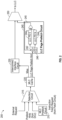
- processor 100 may be any type of processor, ranging from a relatively low power processor having one or a few cores to a larger higher power processor or system on chip (SoC), among others.
- SoC system on chip
- processor 100 is shown with a plurality of cores 110 0 - 110 n .
- cores 110 may be homogeneous or heterogeneous cores. Some details of a representative core 110 0 are shown.
- core 110 0 includes front end circuitry 112, which may be configured to obtain and decode instructions, as well as to obtain data for use in execution of such instructions.
- front end circuitry 112 couples to one or more execution circuits 114 0 - 114 n .
- execution circuits 114 may take the form of arithmetic logic units (ALUs) such as integer and floating point ALUs including scalar and/or vector ALUs, fixed function units or other execution circuitry.
- ALUs arithmetic logic units
- execution circuits 114 couple to various levels of a cache hierarchy.
- core 110 0 includes a data cache unit (DCU) 120 and a mid-level cache (MLC) 130.
- DCU 120 includes a level one (L1) cache 122 and a cache controller 124, which may control the writing and reading of data within L1 cache 122, as well as cache control operations, including cache coherency operations, evictions, insertions, updates and so forth.
- DCU 120 also includes a stream prediction circuit 126.
- stream prediction circuit 126 may be configured to identify a stream of accesses and generate a prediction, e.g., in the form of a last level cache (LLC) page prefetch hint, that can be provided to further levels of the cache hierarchy. While stream prediction circuit 126 may be configured to detect accesses that are for streams of information such as media content (e.g., audio, video or so forth), understand that stream accesses also may include other information types such as add memory copy operations (copying one buffer to another), large array sorting, or accessing any large structure with consecutive accesses.
- LLC last level cache
- stream prediction circuit 126 is separate from cache controller 124 and prefetch operations performed within the cache controller. In this way, these page prefetch operations may proceed independently from other prefetch operations and avoid back pressure or other constraints. Note as further shown, while prefetch requests generated in cache controller 124 may be communicated to MLC 130 via a prefetch main band, LLC page prefetch hints generated in stream prediction circuit 126 may be sent via a separate path to MLC 130. As a result, these prefetch hints are sent in a fire and forget manner.
- prefetch detector 136 may receive incoming LLC page prefetch hints from data cache unit 120 and generate prefetch requests for corresponding lines of a given prefetch page, which may be one or more pages ahead (or behind) of current accesses. Note that such prefetch requests, which may be generated on a per cache line basis, may be communicated as LLC prefetch hints that can be arbitrated with prefetch and demand requests as they are sent via an interconnect such as an intra-die interconnect (IDI) to LLC 150.
- IDI intra-die interconnect
- LLC 150 includes a last level cache memory 152 which may be a shared cache memory and a cache controller 154, which may control the writing and reading of data within cache memory 152. As further shown, LLC 150 also includes a throttler 156, which may monitor bandwidth, capacity and so forth, and provide feedback information based at least in part on this monitoring to MLC 130 and DCU 120. This feedback information in turn may be used to trigger throttling of main path prefetching (and possibly LLC page prefetching). Although shown at this high level in the embodiment of FIG. 1 , many variations and alternatives are possible.
- MLC 200 includes MLC prefetch circuitry that includes a main band MLC prefetch circuit 210 and a separate LLC page prefetch circuit 240.
- MLC cache 220 may include the cache storage elements of MLC 200, along with cache controller circuitry (not shown for ease of illustration).
- incoming prefetch hints from a DCU which may include conventional prefetch hints as well as LLC page prefetch hints in accordance with an embodiment, also are provided to selection circuit 215.
- Selection circuit 215 further may receive additional requests received from one or more external requesters.
- selection circuit 215 may receive instruction fetch requests, which may be received from a fetch circuit such as an instruction fetch circuit, in an embodiment.
- Selection circuit 215 may select from these various sources and provide a request to MLC 220, which may determine whether the requested information is present within it. If not, a miss occurs and a corresponding request may be sent to an interconnect interface circuit 230. Note however that LLC page prefetch hints may instead be sent, upon a miss for the requested data within MLC 220, to LLC page prefetch circuit 240.
- page prefetch circuit 240 receives incoming LLC page prefetch hints. These prefetch hints may be provided to a selected one of multiple LLC page prefetch detectors 244 0 - 244 n .
- these hints may include a page stride value and an offset value.
- the page stride value may indicate a number of pages of stride length at which the prefetch operation is to occur. For example, in a forward direction, a page stride value of two indicates that the prefetch is to begin at a location two pages forward of a page currently accessed. In typical system implementations with 4K page sizes, a page stride value of two thus corresponds to an 8K stride.
- the offset value may indicate an offset into this strided page.
- the page prefetch hints may only include the page stride value and thus prefetch requests may be generated within page prefetch circuit 240 beginning at an offset of zero within the strided page.
- LLC page detectors 244 each may be configured to receive a given page prefetch hint and generate a stream of prefetches in the strided page. For example, where no offset is provided, a given LLC page detector 244 may begin making prefetch requests at an offset of zero. These prefetch requests are provided to a selection circuit 245, which may select a given request, e.g., in round robin fashion. In turn the selected prefetch request is provided to another selection circuit 250. In embodiments herein, selection circuit 250 may select between LLC page prefetch requests and main band traffic received from interconnect interface circuit 230. As such, when high levels of traffic or other blocking conditions exist and limited traffic is sent to interconnect interface circuit 230 by main band circuitry, a relatively high number of page prefetch requests may be sent to the LLC via selection circuit 250.
- the output request also is fed back to an accumulator 242, which may accumulate an offset value, such that a given LLC prefetch detector 244 may send incremented (or decremented) prefetch requests for consecutive cache lines from a strided page. Understand while shown at this high level in the embodiment of FIG. 2 , many variations and alternatives are possible.
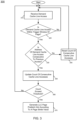
- method 300 of FIG. 3 is a method for predicting a stream access.
- method 300 may be performed by hardware circuitry implemented within a DCU, and in some embodiments may further be implemented using firmware and/or software that executes on this hardware circuitry.
- method 300 may be performed by stream prediction circuit 126 of FIG. 1 .
- method 300 begins by receiving a demand cache line access (block 310).
- This demand access may be received from a requester, e.g., core circuitry, which may issue such demand access when information is being requested.
- a requester e.g., core circuitry
- this request is for information that is needed by an actual path of execution and thus may be differentiated from speculative requests or prefetch requests.
- this demand cache line access is within a trigger window of a given page (diamond 320).
- this trigger window may be within a certain distance to a page boundary, e.g., a beginning or end of a page.
- a trigger window may be identified within another portion of a page, such as a midpoint of a page or so forth.
- this page stride value which may be a configurable value, may be set between, e.g., 2 and 3 in an embodiment.
- this page prefetch hint is issued to start prefetching the cache lines of a page that is the strided value of pages ahead (or behind) of the current page (in a linear or virtual address space) that is being accessed by demand requests.
- this LLC page prefetch is a single prefetch hint that may be used by a LLC page mechanism such as an LLC page detector to in turn generate multiple individual cache line prefetches. Understand while shown at this high level in the embodiment of FIG. 3 , many variations and alternatives are possible.
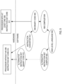
- method 400 of FIG. 4 is a method for performing page prefetching.
- method 400 may be performed by hardware circuitry implemented within a DCU and MLC, and in some embodiments may further be implemented using firmware and/or software that executes on this hardware circuitry.
- this hint which is a prefetch hint for a given cache line within a strided page, is sent to the LLC via the interconnect.
- FIG. 5A is a block diagram illustrating both an exemplary in-order pipeline and an exemplary register renaming, out-of-order issue/execution pipeline according to embodiments of the invention.
- FIG. 5B is a block diagram illustrating both an exemplary embodiment of an in-order architecture core and an exemplary register renaming, out-of-order issue/execution architecture core to be included in a processor according to embodiments of the invention.
- Such embodiments may include decoupled page prefetch mechanisms separate and decoupled from other prefetch circuitry of a processor as described herein.
- 5A and 5B illustrate the in-order pipeline and in-order core, while the optional addition of the dashed lined boxes illustrates the register renaming, out-of-order issue/execution pipeline and core. Given that the in-order aspect is a subset of the out-of-order aspect, the out-of-order aspect will be described.
- a processor pipeline 500 includes a fetch stage 502, a length decode stage 504, a decode stage 506, an allocation stage 508, a renaming stage 510, a scheduling (also known as a dispatch or issue) stage 512, a register read/memory read stage 514, an execute stage 516, a write back/memory write stage 518, an exception handling stage 522, and a commit stage 524.
- a core may include multiple processing pipelines such as pipeline 500.
- FIG. 5B shows processor core 590 including a front end unit 530 coupled to an execution engine unit 550, and both are coupled to a memory unit 570.
- the core 590 may be a reduced instruction set computing (RISC) core, a complex instruction set computing (CISC) core, a very long instruction word (VLIW) core, or a hybrid or alternative core type.
- the core 590 may be a special-purpose core, such as, for example, a network or communication core, compression engine, coprocessor core, general purpose computing graphics processing unit (GPGPU) core, graphics core, or the like.
- GPGPU general purpose computing graphics processing unit
- the front end unit 530 includes a branch prediction unit 532 coupled to a branch target buffer 533 and an instruction cache unit 534, which is coupled to an instruction translation lookaside buffer (TLB) 536, which is coupled to an instruction fetch unit 538, which is coupled to a decode unit 540.
- the decode unit 540 (or decoder) may decode instructions, and generate as an output one or more micro-operations, micro-code entry points, microinstructions, other instructions, or other control signals, which are decoded from, or which otherwise reflect, or are derived from, the original instructions.
- the decode unit 540 may be implemented using various different mechanisms.
- the execution engine unit 550 includes the rename/allocator unit 552 coupled to a retirement unit 554 and a set of one or more scheduler unit(s) 556.
- the scheduler unit(s) 556 represents any number of different schedulers, including reservations stations, central instruction window, etc.
- the scheduler unit(s) 556 is coupled to the physical register file(s) unit(s) 558.
- Each of the physical register file(s) units 558 represents one or more physical register files, different ones of which store one or more different data types, such as scalar integer, scalar floating point, packed integer, packed floating point, vector integer, vector floating point, status (e.g., an instruction pointer that is the address of the next instruction to be executed), etc.
- the physical register file(s) unit 558 comprises a vector registers unit, a write mask registers unit, and a scalar registers unit. These register units may provide architectural vector registers, vector mask registers, and general purpose registers.
- the data cache unit 574 may include a streaming detection circuit 575 in accordance with embodiments to detect streaming accesses as described herein.
- the L2 cache unit 576 includes a prefetcher circuit 578 and a separate decoupled page prefetch circuit 579, as described herein.
- the instruction cache unit 534 is further coupled to the L2 cache unit 576 in the memory unit 570.
- the L2 cache unit 576 is coupled to one or more other levels of cache and eventually to a main memory.
- the core 590 may support one or more instructions sets (e.g., the x86 instruction set (with some extensions that have been added with newer versions); the MIPS instruction set of MIPS Technologies of Sunnyvale, CA; the ARM instruction set (with optional additional extensions such as NEON) of ARM Holdings of Sunnyvale, CA), including the instruction(s) described herein.
- the core 590 includes logic to support a packed data instruction set extension (e.g., AVX1, AVX2), thereby allowing the operations used by many multimedia applications to be performed using packed data.
- a packed data instruction set extension e.g., AVX1, AVX2
- the core may support multithreading (executing two or more parallel sets of operations or threads), and may do so in a variety of ways including time sliced multithreading, simultaneous multithreading (where a single physical core provides a logical core for each of the threads that physical core is simultaneously multithreading), or a combination thereof (e.g., time sliced fetching and decoding and simultaneous multithreading thereafter such as in the Intel ® Hyperthreading technology).
- register renaming is described in the context of out-of-order execution, it should be understood that register renaming may be used in an in-order architecture.
- the illustrated embodiment of the processor also includes separate instruction and data cache units 534/574 and a shared L2 cache unit 576, alternative embodiments may have a single internal cache for both instructions and data, such as, for example, a Level 1 (L1) internal cache, or multiple levels of internal cache.
- the system may include a combination of an internal cache and an external cache that is external to the core and/or the processor. Alternatively, all of the cache may be external to the core and/or the processor.
- FIG. 6 is a block diagram of a processor 600 that may have more than one core, may have an integrated memory controller, and may have integrated graphics according to embodiments of the invention.
- the solid lined boxes in FIG. 6 illustrate a processor 600 with a single core 602A, a system agent 610, a set of one or more bus controller units 616, while the optional addition of the dashed lined boxes illustrates an alternative processor 600 with multiple cores 602A-N, a set of one or more integrated memory controller unit(s) in the system agent unit 610, and a special purpose logic 608, which may perform one or more specific functions.
- different implementations of the processor 600 may include: 1) a CPU with a special purpose logic being integrated graphics and/or scientific (throughput) logic (which may include one or more cores), and the cores 602A-N being one or more general purpose cores (e.g., general purpose in-order cores, general purpose out-of-order cores, a combination of the two); 2) a coprocessor with the cores 602A-N being a large number of special purpose cores intended primarily for graphics and/or scientific (throughput); and 3) a coprocessor with the cores 602A-N being a large number of general purpose in-order cores.
- a CPU with a special purpose logic being integrated graphics and/or scientific (throughput) logic which may include one or more cores
- the cores 602A-N being one or more general purpose cores (e.g., general purpose in-order cores, general purpose out-of-order cores, a combination of the two)
- the processor 600 may be a general-purpose processor, coprocessor or special-purpose processor, such as, for example, a network or communication processor, compression engine, graphics processor, GPGPU (general purpose graphics processing unit), a high-throughput many integrated core (MIC) coprocessor (including 30 or more cores), embedded processor, or the like.
- the processor may be implemented on one or more chips.
- the processor 600 may be a part of and/or may be implemented on one or more substrates using any of a number of process technologies, such as, for example, BiCMOS, CMOS, or NMOS.
- the memory hierarchy includes one or more levels of cache units 604A-N within the cores, a set or one or more shared cache units 606, and external memory (not shown) coupled to the set of integrated memory controller units 614.
- the set of shared cache units 606 may include one or more mid-level caches, such as level 2 (L2), level 3 (L3), level 4 (L4), or other levels of cache, a last level cache (LLC), and/or combinations thereof. While in one embodiment a ring based interconnect unit 612 interconnects the special purpose 608, the set of shared cache units 606, and the system agent unit 610/integrated memory controller unit(s) 614, alternative embodiments may use any number of well-known techniques for interconnecting such units.
- the system agent unit 610 includes those components coordinating and operating cores 602A-N.
- the system agent unit 610 may include for example a power control unit (PCU) and a display unit.
- the PCU may be or include logic and components needed for regulating the power state of the cores 602A-N and the special purpose logic 608.
- the display unit is for driving one or more externally connected displays.
- the cores 602A-N may be homogenous or heterogeneous in terms of architecture instruction set; that is, two or more of the cores 602A-N may be capable of execution the same instruction set, while others may be capable of executing only a subset of that instruction set or a different instruction set.
- the cores 602A-N may include decoupled page prefetch circuitry as described herein.
- FIGS. 7-8 are block diagrams of exemplary computer architectures.
- Other system designs and configurations known in the arts for laptops, desktops, handheld PCs, personal digital assistants, engineering workstations, servers, network devices, network hubs, switches, embedded processors, digital signal processors (DSPs), graphics devices, video game devices, set-top boxes, micro controllers, cell phones, portable media players, hand held devices, and various other electronic devices, are also suitable.
- DSPs digital signal processors
- graphics devices video game devices, set-top boxes, micro controllers, cell phones, portable media players, hand held devices, and various other electronic devices, are also suitable.
- DSPs digital signal processors
- FIGS. 7-8 are block diagrams of exemplary computer architectures.
- multiprocessor system 700 is a point-to-point interconnect system, and includes a first processor 770 and a second processor 780 coupled via a point-to-point interconnect 750.
- processors 770 and 780 may be some version of the processor 600.
- Processors 770, 780 may each exchange information with a chipset 790 via individual P-P interfaces 752, 754 using point to point interface circuits 776, 794, 786, 798.
- Chipset 790 may optionally exchange information with the coprocessor 738 via a high-performance interface 739.
- the coprocessor 738 is a special-purpose processor, such as, for example, a high-throughput MIC processor, a network or communication processor, compression engine, graphics processor, GPGPU, embedded processor, or the like.
- first bus 716 may be a Peripheral Component Interconnect (PCI) bus, or a bus such as a PCI Express bus or another third generation I/O interconnect bus, although the scope of the present invention is not so limited.
- PCI Peripheral Component Interconnect
- Various devices may be coupled to a second bus 720 including, for example, a keyboard and/or mouse 722, communication devices 727 and a storage unit 728 such as a disk drive or other mass storage device which may include instructions/code and data 730, in one embodiment.
- a storage unit 728 such as a disk drive or other mass storage device which may include instructions/code and data 730, in one embodiment.
- an audio I/O 724 may be coupled to the second bus 720.
- FIG. 7 a system may implement a multi-drop bus or other such architecture.
- an interconnect unit(s) 802 is coupled to: an application processor 810 which includes a set of one or more cores 802A-N (including constituent cache units 804AN) at least some of which may include page prefetch circuitry separate and decoupled from other prefetch circuitry as described herein; shared cache unit(s) 806; a system agent unit 812; a bus controller unit(s) 816; an integrated memory controller unit(s) 814; a set or one or more coprocessors 820 which may include integrated graphics logic, an image processor, an audio processor, and a video processor; a static random access memory (SRAM) unit 830; a direct memory access (DMA) unit 832; and a display unit 840 for coupling to one or more external displays.
- the coprocessor(s) 820 which may include integrated graphics logic, an image processor, an audio processor, and a video processor; a static random access memory (SRAM) unit 830; a direct memory access (DMA) unit 832; and a display unit
- Embodiments of the mechanisms disclosed herein may be implemented in hardware, software, firmware, or a combination of such implementation approaches.
- Embodiments of the invention may be implemented as computer programs or program code executing on programmable systems comprising at least one processor, a storage system (including volatile and non-volatile memory and/or storage elements), at least one input device, and at least one output device.
- Program code such as code 730 illustrated in FIG. 7
- Program code may be applied to input instructions to perform the functions described herein and generate output information.
- the output information may be applied to one or more output devices, in known fashion.
- a processing system includes any system that has a processor, such as, for example; a digital signal processor (DSP), a microcontroller, an application specific integrated circuit (ASIC), or a microprocessor.
- DSP digital signal processor
- ASIC application specific integrated circuit
- the program code may be implemented in a high level procedural or object oriented programming language to communicate with a processing system.
- the program code may also be implemented in assembly or machine language, if desired.
- the mechanisms described herein are not limited in scope to any particular programming language. In any case, the language may be a compiled or interpreted language.
- IP cores may be stored on a tangible, machine readable medium and supplied to various customers or manufacturing facilities to load into the fabrication machines that actually make the logic or processor.
- Such machine-readable storage media may include, without limitation, non-transitory, tangible arrangements of articles manufactured or formed by a machine or device, including storage media such as hard disks, any other type of disk including floppy disks, optical disks, compact disk read-only memories (CD-ROMs), compact disk rewritable's (CD-RWs), and magneto-optical disks, semiconductor devices such as read-only memories (ROMs), random access memories (RAMs) such as dynamic random access memories (DRAMs), static random access memories (SRAMs), erasable programmable read-only memories (EPROMs), flash memories, electrically erasable programmable read-only memories (EEPROMs), phase change memory (PCM), magnetic or optical cards, or any other type of media suitable for storing electronic instructions.
- storage media such as hard disks, any other type of disk including floppy disks, optical disks, compact disk read-only memories (CD-ROMs), compact disk rewritable's (CD-RWs), and magneto
- embodiments of the invention also include non-transitory, tangible machine-readable media containing instructions or containing design data, such as Hardware Description Language (HDL), which defines structures, circuits, apparatuses, processors and/or system features described herein.
- HDL Hardware Description Language
- Such embodiments may also be referred to as program products.
- an instruction converter may be used to convert an instruction from a source instruction set to a target instruction set.
- the instruction converter may translate (e.g., using static binary translation, dynamic binary translation including dynamic compilation), morph, emulate, or otherwise convert an instruction to one or more other instructions to be processed by the core.
- the instruction converter may be implemented in software, hardware, firmware, or a combination thereof.
- the instruction converter may be on processor, off processor, or part on and part off processor.
- FIG. 9 is a block diagram contrasting the use of a software instruction converter to convert binary instructions in a source instruction set to binary instructions in a target instruction set according to embodiments of the invention.
- the instruction converter is a software instruction converter, although alternatively the instruction converter may be implemented in software, firmware, hardware, or various combinations thereof.
- FIG. 9 shows a program in a high level language 902 may be compiled using an x86 compiler 904 to generate x86 binary code 906 that may be natively executed by a processor with at least one x86 instruction set core 916.
- the processor with at least one x86 instruction set core 916 represents any processor that can perform substantially the same functions as an Intel processor with at least one x86 instruction set core by compatibly executing or otherwise processing (1) a substantial portion of the instruction set of the Intel x86 instruction set core or (2) object code versions of applications or other software targeted to run on an Intel processor with at least one x86 instruction set core, in order to achieve substantially the same result as an Intel processor with at least one x86 instruction set core.
- the x86 compiler 904 represents a compiler that is operable to generate x86 binary code 906 (e.g., object code) that can, with or without additional linkage processing, be executed on the processor with at least one x186 instruction set core 916.
- FIG. 9 shows the program in the high level language 902 may be compiled using an alternative instruction set compiler 908 to generate alternative instruction set binary code 910 that may be natively executed by a processor without at least one x86 instruction set core 914 (e.g., a processor with cores that execute the MIPS instruction set of MIPS Technologies of Sunnyvale, CA and/or that execute the ARM instruction set of ARM Holdings of Sunnyvale, CA).
- the instruction converter 912 is used to convert the x86 binary code 906 into code that may be natively executed by the processor without an x86 instruction set core 914.
- the processor may further comprise a data cache unit comprising a first cache memory and the stream prediction circuit.
- the processor may further comprise a mid-level cache comprising a second cache memory and the prefetcher circuit, where the data cache unit is to send the page prefetch hint to the mid-level cache when the page prefetch hint misses in the first cache memory.
- the processor may further comprise an interconnect interface circuit to receive the second prefetch requests and the first prefetch requests and direct at least some of the second prefetch requests and at least some of the first prefetch requests to a shared cache memory.
- the interconnect interface circuit may be to send the second prefetch requests when the prefetcher circuit is stalled.
- the processor may further comprise a plurality of page detectors each to receive a page prefetch hint and to generate a plurality of prefetch requests based on the page prefetch hint.
- a first page detector may be to receive the page prefetch hint and to generate the plurality of prefetch requests for a first page based at least in part on a page stride value of the page prefetch hint.
- the processor may further comprise a throttler to throttle the stream prediction circuit based at least in part on a stress level.
- a method comprises: receiving, in a second cache memory of a processor, a page prefetch hint from a first cache memory of the processor, wherein the page prefetch hint is generated, based at least in part on received demand requests for information, by a stream prediction circuit coupled to one or more execution circuits, the stream prediction circuit decoupled from a prefetcher circuit; allocating a page prefetch detector for the page prefetch hint; generating, in the page prefetch detector, a plurality of first prefetch requests based on the page prefetch hint; and sending the plurality of first prefetch requests to a shared cache memory of the processor in available slots of an interconnect coupled between the second cache memory and the shared cache memory.
- the method may further comprise arbitrating between the plurality of first prefetch requests and a plurality of second prefetch requests, the plurality of first prefetch requests for a first page located at a distance according to a page stride value from a second page to which the plurality of second prefetch requests are directed.
- the method may further comprise receiving the page prefetch hint comprising a page hint portion and offset hint portion, the page hint portion for two or more pages removed from a current demand access page.
- the method may further comprise: maintaining a count of consecutive cache line accesses for a second page; when the count meets a threshold level, generating the page prefetch hint in the first cache memory, the page prefetch hint for a first page that is at least two pages distance from the second page; and sending the page prefetch hint to the second cache memory.
- the method may further comprise resetting the count of consecutive cache lines in response to a non-consecutive cache line request.
- the method may further comprise updating the count of consecutive cache line accesses in response to a next consecutive cache line request.
- a computer readable medium including data may be used by at least one machine to fabricate at least one integrated circuit to perform the method of any one of the above examples.
- an apparatus may comprise means for performing the method of any one of the above embodiments and examples.
- a system may comprise a SoC and a system memory coupled to the SoC.
- the SoC may include: one or more execution circuits to execute instructions; a first cache memory coupled to the one or more execution circuits, the first cache memory comprising a stream prediction circuit to receive demand requests for information in a first page and, based at least in part on the demand requests, generate a page prefetch hint for a second page; and a second cache memory coupled to the first cache memory.
- the second cache memory may include: a first prefetch circuit to generate first prefetch requests; and a page prefetch circuit to generate second prefetch requests based on the page prefetch hint, where the page prefetch circuit is decoupled from the first prefetch circuit.
- the system memory may send first information from the first page to the SoC in response to the first prefetch requests and send second information from the second page to the SoC in response to the second prefetch requests.
- the first prefetch circuit may comprise a main band prefetch circuit.
- system may further comprise an interface circuit coupled to the first prefetch circuit and the page prefetch circuit, where the interface circuit is to send a plurality of the second prefetch requests to a third cache memory when the first prefetch circuit is stalled.
- the interface circuit may be to handle the first prefetch requests with a higher priority than the second prefetch requests.
- the page prefetch circuit may be to generate the second prefetch requests for the second page, the second page removed from the first page having a triggering address for the page prefetch hint.
- circuit and “circuitry” are used interchangeably herein.
- logic are used to refer to alone or in any combination, analog circuitry, digital circuitry, hard wired circuitry, programmable circuitry, processor circuitry, microcontroller circuitry, hardware logic circuitry, state machine circuitry and/or any other type of physical hardware component.
- Embodiments may be used in many different types of systems. For example, in one embodiment a communication device can be arranged to perform the various methods and techniques described herein.
- the scope of the present invention is not limited to a communication device, and instead other embodiments can be directed to other types of apparatus for processing instructions, or one or more machine readable media including instructions that in response to being executed on a computing device, cause the device to carry out one or more of the methods and techniques described herein.
- Embodiments may be implemented in code and may be stored on a non-transitory storage medium having stored thereon instructions which can be used to program a system to perform the instructions. Embodiments also may be implemented in data and may be stored on a non-transitory storage medium, which if used by at least one machine, causes the at least one machine to fabricate at least one integrated circuit to perform one or more operations. Still further embodiments may be implemented in a computer readable storage medium including information that, when manufactured into a SoC or other processor, is to configure the SoC or other processor to perform one or more operations.
- the storage medium may include, but is not limited to, any type of disk including floppy disks, optical disks, solid state drives (SSDs), compact disk read-only memories (CD-ROMs), compact disk rewritables (CD-RWs), and magneto-optical disks, semiconductor devices such as read-only memories (ROMs), random access memories (RAMs) such as dynamic random access memories (DRAMs), static random access memories (SRAMs), erasable programmable read-only memories (EPROMs), flash memories, electrically erasable programmable read-only memories (EEPROMs), magnetic or optical cards, or any other type of media suitable for storing electronic instructions.
- ROMs read-only memories
- RAMs random access memories
- DRAMs dynamic random access memories
- SRAMs static random access memories
- EPROMs erasable programmable read-only memories
- EEPROMs electrically erasable programmable read-only memories
- magnetic or optical cards or any other type of media suitable for storing electronic instructions.
Landscapes
- Engineering & Computer Science (AREA)
- Theoretical Computer Science (AREA)
- General Engineering & Computer Science (AREA)
- Physics & Mathematics (AREA)
- General Physics & Mathematics (AREA)
- Computer Hardware Design (AREA)
- Software Systems (AREA)
- Computing Systems (AREA)
- Microelectronics & Electronic Packaging (AREA)
- Memory System Of A Hierarchy Structure (AREA)
Claims (13)
- Prozessor (100), der Folgendes umfasst:eine oder mehrere Ausführungsschaltungen (1140, 1141, ..., 114n), um Anweisungen auszuführen;eine Stromvorhersageschaltung (126), die mit der einen oder den mehreren Ausführungsschaltungen (1140, 1141, ..., 114n) gekoppelt ist, wobei die Stromvorhersageschaltung (126) Anforderungsanfragen nach Informationen empfängt und, zumindest teilweise basierend auf den Anforderungsanfragen, einen Seitenvorabrufhinweis für eine erste Seite erzeugt;eine Vorabrufschaltung (135), um erste Vorabrufanfragen jeweils für eine Cachezeile zu erzeugen, wobei die Stromvorhersageschaltung (126) von der Vorabrufschaltung (135) entkoppelt ist; gekennzeichnet durch:mehrere Seitendetektoren (2440, 2441, ..., 244n), die jeweils den Seitenvorabrufhinweis empfangen und mehrere zweite Vorabrufanfragen basierend auf dem Seitenvorabrufhinweis erzeugen sollen; undeinen gemeinsam genutzten Cachespeicher (152), der mit der Stromvorhersageschaltung (126) und der Vorabrufschaltung (135) gekoppelt ist, wobei der gemeinsam genutzte Cachespeicher (152) zweite Vorabrufanfragen empfangen soll, die mit dem Seitenvorabrufhinweis und mindestens einigen der ersten Vorabrufanfragen assoziiert sind, wobei die zweiten Vorabrufanfragen für eine andere Seite als die ersten Vorabrufanfragen sind.
- Prozessor (100) nach Anspruch 1, der ferner eine Daten-Cache-Einheit (120) umfasst, die einen ersten Cachespeicher (122) und die Stromvorhersageschaltung (126) umfasst.
- Prozessor (100) nach Anspruch 2, der ferner einen Mid-Level-Cache (130) umfasst, der einen zweiten Cachespeicher (132) und die Vorabrufschaltung (135) umfasst, wobei die Daten-Cache-Einheit (120) den Seitenvorabrufhinweis an den Mid-Level-Cache (130) senden soll, wenn der Seitenvorabrufhinweis in dem ersten Cachespeicher (122) fehlschlägt.
- Prozessor (100) nach Anspruch 1, der ferner eine Zwischenverbindungsschnittstellenschaltung (230) umfasst, um die zweiten Vorabrufanfragen und die ersten Vorabrufanfragen zu empfangen und mindestens einige der zweiten Vorabrufanfragen und mindestens einige der ersten Vorabrufanfragen an einen gemeinsam genutzten Cachespeicher (152) zu leiten.
- Prozessor (100) nach Anspruch 4, wobei die Zwischenverbindungsschnittstellenschaltung (230) die zweiten Vorabrufanfragen senden soll, wenn die Vorabrufschaltung (135) gestoppt ist.
- Prozessor (100) nach Anspruch 1, wobei ein erster Seitendetektor (244) den Seitenvorabrufhinweis empfangen und die mehreren Vorabrufanfragen für eine erste Seite zumindest teilweise basierend auf einem Seitenschrittwert des Seitenvorabrufhinweises erzeugen soll.
- Prozessor (100) nach einem der Ansprüche 1 bis 6, der ferner einen Drossler (138) umfasst, um die Stromvorhersageschaltung (126) zumindest teilweise basierend auf einem Belastungspegel zu drosseln.
- Verfahren (400), das Folgendes umfasst:Empfangen (435), in einem zweiten Cachespeicher (132) eines Prozessors (100), eines Seitenvorabrufhinweises von einem ersten Cachespeicher (122) des Prozessors (100), wobei der Seitenvorabrufhinweis zumindest teilweise basierend auf empfangenen Anforderungsanfragen für Informationen durch eine Stromvorhersageschaltung (126) erzeugt wird, die mit einer oder mehreren Ausführungsschaltungen (1141, 1142, ..., 144n) gekoppelt ist, wobei die Stromvorhersageschaltung (126) von einer Vorabrufschaltung (135) entkoppelt ist; Empfangen des Seitenvorabrufhinweises durch mehrere Seitendetektoren (2440, 2441, ..., 244n) und Erzeugen mehrerer zweiter Vorabrufanfragen basierend auf dem Seitenvorabrufhinweis;Zuweisen (450) eines Seitenvorabrufdetektors (244) für den Seitenvorabrufhinweis;Erzeugen, in dem Seitenvorabrufdetektor (244), mehrerer erster Vorabrufanfragen basierend auf dem Seitenvorabrufhinweis; undSenden (460) der mehreren ersten Vorabrufanfragen an einen gemeinsam genutzten Cachespeicher (152) des Prozessors (100) in verfügbaren Schlitzen einer Zwischenverbindung, die zwischen dem zweiten Cachespeicher (132) und dem gemeinsam genutzten Cachespeicher (152) gekoppelt ist, Senden zweiter Vorabrufanfragen, die mit dem Seitenvorabrufhinweis assoziiert sind, an den gemeinsam genutzten Cachespeicher (152), wobei die zweiten Vorabrufanfragen für eine andere Seite als die ersten Vorabrufanfragen sind.
- Verfahren (400) nach Anspruch 8, das ferner Vermitteln zwischen den mehreren ersten Vorabrufanfragen und mehreren zweiten Vorabrufanfragen umfasst, wobei sich die mehreren ersten Vorabrufanfragen für eine erste Seite in einem Abstand gemäß einem Seitenschrittwert von einer zweiten Seite befinden, an die die mehreren zweiten Vorabrufanfragen gerichtet sind.
- Verfahren (400) nach Anspruch 8, das ferner das Empfangen des Seitenvorabrufhinweises umfasst, der einen Seitenhinweisteil und einen Versatzhinweisteil umfasst, wobei der Seitenhinweisteil für zwei oder mehr Seiten von einer aktuellen Bedarfszugriffsseite entfernt ist.
- Verfahren (400) nach Anspruch 8, das ferner Folgendes umfasst:Aufrechterhalten einer Anzahl aufeinanderfolgender Cachezeilenzugriffe für eine zweite Seite;wenn die Anzahl einen Schwellenpegel erfüllt, Erzeugen des Seitenvorabrufhinweises in dem ersten Cachespeicher (122), des Seitenvorabrufhinweises für eine erste Seite, die mindestens zwei Seiten von der zweiten Seite entfernt ist; undSenden des Seitenvorabrufhinweises an den zweiten Cachespeicher (132).
- Zumindest ein computerlesbares Speichermedium, auf dem Anweisungen gespeichert sind, die, wenn sie von einer Maschine durchgeführt werden, die Maschine veranlassen, das Verfahren nach einem der Ansprüche 9 bis 11 durchzuführen.
- Vorrichtung, die Mittel umfasst, um ein Verfahren nach einem der Ansprüche 9 bis 11 durchzuführen.
Applications Claiming Priority (1)
| Application Number | Priority Date | Filing Date | Title |
|---|---|---|---|
| US17/130,696 US12019553B2 (en) | 2020-12-22 | 2020-12-22 | System, apparatus and method for prefetching physical pages in a processor |
Publications (2)
| Publication Number | Publication Date |
|---|---|
| EP4020229A1 EP4020229A1 (de) | 2022-06-29 |
| EP4020229B1 true EP4020229B1 (de) | 2025-02-26 |
Family
ID=77910711
Family Applications (1)
| Application Number | Title | Priority Date | Filing Date |
|---|---|---|---|
| EP21198548.6A Active EP4020229B1 (de) | 2020-12-22 | 2021-09-23 | System, vorrichtung und verfahren zum prefetching von physikalischen seiten in einem prozessor |
Country Status (3)
| Country | Link |
|---|---|
| US (1) | US12019553B2 (de) |
| EP (1) | EP4020229B1 (de) |
| CN (1) | CN114661357A (de) |
Families Citing this family (4)
| Publication number | Priority date | Publication date | Assignee | Title |
|---|---|---|---|---|
| US12282428B2 (en) * | 2021-12-28 | 2025-04-22 | Advanced Micro Devices, Inc. | Selective speculative prefetch requests for a last-level cache |
| US12164429B2 (en) * | 2022-08-19 | 2024-12-10 | Qualcomm Incorporated | Stride-based prefetcher circuits for prefetching next stride(s) into cache memory based on identified cache access stride patterns, and related processor-based systems and methods |
| WO2024177904A1 (en) * | 2023-02-21 | 2024-08-29 | Xilinx, Inc. | Configurable engine embedded into a processor for managing cache data flows |
| US20260072843A1 (en) * | 2024-09-10 | 2026-03-12 | Apple Inc. | Adaptive Adjustment of Prefetch Constraints for Certain Workloads |
Family Cites Families (7)
| Publication number | Priority date | Publication date | Assignee | Title |
|---|---|---|---|---|
| US5822790A (en) | 1997-02-07 | 1998-10-13 | Sun Microsystems, Inc. | Voting data prefetch engine |
| US20070101100A1 (en) * | 2005-10-28 | 2007-05-03 | Freescale Semiconductor, Inc. | System and method for decoupled precomputation prefetching |
| US9418013B2 (en) * | 2014-06-30 | 2016-08-16 | Intel Corporation | Selective prefetching for a sectored cache |
| US10157136B2 (en) | 2016-03-31 | 2018-12-18 | Intel Corporation | Pipelined prefetcher for parallel advancement of multiple data streams |
| US20200104259A1 (en) | 2018-09-28 | 2020-04-02 | Intel Corporation | System, method, and apparatus for snapshot prefetching to improve performance of snapshot operations |
| US11249909B2 (en) | 2018-12-28 | 2022-02-15 | Intel Corporation | Systems and methods for adaptive multipath probability (AMP) prefetcher |
| US11176045B2 (en) * | 2020-03-27 | 2021-11-16 | Apple Inc. | Secondary prefetch circuit that reports coverage to a primary prefetch circuit to limit prefetching by primary prefetch circuit |
-
2020
- 2020-12-22 US US17/130,696 patent/US12019553B2/en active Active
-
2021
- 2021-09-23 EP EP21198548.6A patent/EP4020229B1/de active Active
- 2021-11-19 CN CN202111374725.3A patent/CN114661357A/zh active Pending
Also Published As
| Publication number | Publication date |
|---|---|
| CN114661357A (zh) | 2022-06-24 |
| US20220197808A1 (en) | 2022-06-23 |
| US12019553B2 (en) | 2024-06-25 |
| EP4020229A1 (de) | 2022-06-29 |
Similar Documents
| Publication | Publication Date | Title |
|---|---|---|
| US11243775B2 (en) | System, apparatus and method for program order queue (POQ) to manage data dependencies in processor having multiple instruction queues | |
| JP5372929B2 (ja) | 階層マイクロコードストアを有するマルチコアプロセッサ | |
| US10303609B2 (en) | Independent tuning of multiple hardware prefetchers | |
| KR101614867B1 (ko) | 데이터 스트림에 대한 저장 인식 프리페치 | |
| EP4020229B1 (de) | System, vorrichtung und verfahren zum prefetching von physikalischen seiten in einem prozessor | |
| US11188341B2 (en) | System, apparatus and method for symbolic store address generation for data-parallel processor | |
| CN103620555B (zh) | 抑制不正确的推测性执行路径上的控制转移指令 | |
| US11030108B2 (en) | System, apparatus and method for selective enabling of locality-based instruction handling | |
| US10482017B2 (en) | Processor, method, and system for cache partitioning and control for accurate performance monitoring and optimization | |
| US11531562B2 (en) | Systems, methods, and apparatuses for resource monitoring | |
| CN108694136B (zh) | 用于超越基于非局部性的指令处理的系统、设备和方法 | |
| US11847053B2 (en) | Apparatuses, methods, and systems for a duplication resistant on-die irregular data prefetcher | |
| US11182298B2 (en) | System, apparatus and method for dynamic profiling in a processor | |
| CN112395000B (zh) | 一种数据预加载方法和指令处理装置 | |
| US20180165200A1 (en) | System, apparatus and method for dynamic profiling in a processor | |
| EP4155915B1 (de) | Skalierbare umschaltpunkt-steuerschaltung für eine cluster-decodierpipeline | |
| US20210200538A1 (en) | Dual write micro-op queue |
Legal Events
| Date | Code | Title | Description |
|---|---|---|---|
| PUAI | Public reference made under article 153(3) epc to a published international application that has entered the european phase |
Free format text: ORIGINAL CODE: 0009012 |
|
| STAA | Information on the status of an ep patent application or granted ep patent |
Free format text: STATUS: THE APPLICATION HAS BEEN PUBLISHED |
|
| AK | Designated contracting states |
Kind code of ref document: A1 Designated state(s): AL AT BE BG CH CY CZ DE DK EE ES FI FR GB GR HR HU IE IS IT LI LT LU LV MC MK MT NL NO PL PT RO RS SE SI SK SM TR |
|
| STAA | Information on the status of an ep patent application or granted ep patent |
Free format text: STATUS: REQUEST FOR EXAMINATION WAS MADE |
|
| 17P | Request for examination filed |
Effective date: 20221219 |
|
| RBV | Designated contracting states (corrected) |
Designated state(s): AL AT BE BG CH CY CZ DE DK EE ES FI FR GB GR HR HU IE IS IT LI LT LU LV MC MK MT NL NO PL PT RO RS SE SI SK SM TR |
|
| GRAP | Despatch of communication of intention to grant a patent |
Free format text: ORIGINAL CODE: EPIDOSNIGR1 |
|
| STAA | Information on the status of an ep patent application or granted ep patent |
Free format text: STATUS: GRANT OF PATENT IS INTENDED |
|
| INTG | Intention to grant announced |
Effective date: 20240927 |
|
| GRAS | Grant fee paid |
Free format text: ORIGINAL CODE: EPIDOSNIGR3 |
|
| GRAA | (expected) grant |
Free format text: ORIGINAL CODE: 0009210 |
|
| STAA | Information on the status of an ep patent application or granted ep patent |
Free format text: STATUS: THE PATENT HAS BEEN GRANTED |
|
| AK | Designated contracting states |
Kind code of ref document: B1 Designated state(s): AL AT BE BG CH CY CZ DE DK EE ES FI FR GB GR HR HU IE IS IT LI LT LU LV MC MK MT NL NO PL PT RO RS SE SI SK SM TR |
|
| REG | Reference to a national code |
Ref country code: GB Ref legal event code: FG4D |
|
| REG | Reference to a national code |
Ref country code: CH Ref legal event code: EP |
|
| REG | Reference to a national code |
Ref country code: DE Ref legal event code: R096 Ref document number: 602021026689 Country of ref document: DE |
|
| P01 | Opt-out of the competence of the unified patent court (upc) registered |
Free format text: CASE NUMBER: APP_6589/2025 Effective date: 20250207 |
|
| REG | Reference to a national code |
Ref country code: IE Ref legal event code: FG4D |
|
| REG | Reference to a national code |
Ref country code: NL Ref legal event code: FP |
|
| PG25 | Lapsed in a contracting state [announced via postgrant information from national office to epo] |
Ref country code: RS Free format text: LAPSE BECAUSE OF FAILURE TO SUBMIT A TRANSLATION OF THE DESCRIPTION OR TO PAY THE FEE WITHIN THE PRESCRIBED TIME-LIMIT Effective date: 20250526 |
|
| PG25 | Lapsed in a contracting state [announced via postgrant information from national office to epo] |
Ref country code: FI Free format text: LAPSE BECAUSE OF FAILURE TO SUBMIT A TRANSLATION OF THE DESCRIPTION OR TO PAY THE FEE WITHIN THE PRESCRIBED TIME-LIMIT Effective date: 20250226 |
|
| PG25 | Lapsed in a contracting state [announced via postgrant information from national office to epo] |
Ref country code: PL Free format text: LAPSE BECAUSE OF FAILURE TO SUBMIT A TRANSLATION OF THE DESCRIPTION OR TO PAY THE FEE WITHIN THE PRESCRIBED TIME-LIMIT Effective date: 20250226 |
|
| PG25 | Lapsed in a contracting state [announced via postgrant information from national office to epo] |
Ref country code: ES Free format text: LAPSE BECAUSE OF FAILURE TO SUBMIT A TRANSLATION OF THE DESCRIPTION OR TO PAY THE FEE WITHIN THE PRESCRIBED TIME-LIMIT Effective date: 20250226 |
|
| REG | Reference to a national code |
Ref country code: LT Ref legal event code: MG9D |
|
| PG25 | Lapsed in a contracting state [announced via postgrant information from national office to epo] |
Ref country code: NO Free format text: LAPSE BECAUSE OF FAILURE TO SUBMIT A TRANSLATION OF THE DESCRIPTION OR TO PAY THE FEE WITHIN THE PRESCRIBED TIME-LIMIT Effective date: 20250526 Ref country code: IS Free format text: LAPSE BECAUSE OF FAILURE TO SUBMIT A TRANSLATION OF THE DESCRIPTION OR TO PAY THE FEE WITHIN THE PRESCRIBED TIME-LIMIT Effective date: 20250626 |
|
| PG25 | Lapsed in a contracting state [announced via postgrant information from national office to epo] |
Ref country code: HR Free format text: LAPSE BECAUSE OF FAILURE TO SUBMIT A TRANSLATION OF THE DESCRIPTION OR TO PAY THE FEE WITHIN THE PRESCRIBED TIME-LIMIT Effective date: 20250226 |
|
| PG25 | Lapsed in a contracting state [announced via postgrant information from national office to epo] |
Ref country code: PT Free format text: LAPSE BECAUSE OF FAILURE TO SUBMIT A TRANSLATION OF THE DESCRIPTION OR TO PAY THE FEE WITHIN THE PRESCRIBED TIME-LIMIT Effective date: 20250626 Ref country code: LV Free format text: LAPSE BECAUSE OF FAILURE TO SUBMIT A TRANSLATION OF THE DESCRIPTION OR TO PAY THE FEE WITHIN THE PRESCRIBED TIME-LIMIT Effective date: 20250226 |
|
| PG25 | Lapsed in a contracting state [announced via postgrant information from national office to epo] |
Ref country code: GR Free format text: LAPSE BECAUSE OF FAILURE TO SUBMIT A TRANSLATION OF THE DESCRIPTION OR TO PAY THE FEE WITHIN THE PRESCRIBED TIME-LIMIT Effective date: 20250527 Ref country code: BG Free format text: LAPSE BECAUSE OF FAILURE TO SUBMIT A TRANSLATION OF THE DESCRIPTION OR TO PAY THE FEE WITHIN THE PRESCRIBED TIME-LIMIT Effective date: 20250226 |
|
| REG | Reference to a national code |
Ref country code: AT Ref legal event code: MK05 Ref document number: 1771330 Country of ref document: AT Kind code of ref document: T Effective date: 20250226 |
|
| PGFP | Annual fee paid to national office [announced via postgrant information from national office to epo] |
Ref country code: NL Payment date: 20250704 Year of fee payment: 5 |
|
| PG25 | Lapsed in a contracting state [announced via postgrant information from national office to epo] |
Ref country code: SE Free format text: LAPSE BECAUSE OF FAILURE TO SUBMIT A TRANSLATION OF THE DESCRIPTION OR TO PAY THE FEE WITHIN THE PRESCRIBED TIME-LIMIT Effective date: 20250226 |
|
| PG25 | Lapsed in a contracting state [announced via postgrant information from national office to epo] |
Ref country code: SM Free format text: LAPSE BECAUSE OF FAILURE TO SUBMIT A TRANSLATION OF THE DESCRIPTION OR TO PAY THE FEE WITHIN THE PRESCRIBED TIME-LIMIT Effective date: 20250226 |
|
| PG25 | Lapsed in a contracting state [announced via postgrant information from national office to epo] |
Ref country code: DK Free format text: LAPSE BECAUSE OF FAILURE TO SUBMIT A TRANSLATION OF THE DESCRIPTION OR TO PAY THE FEE WITHIN THE PRESCRIBED TIME-LIMIT Effective date: 20250226 |
|
| PGFP | Annual fee paid to national office [announced via postgrant information from national office to epo] |
Ref country code: DE Payment date: 20250819 Year of fee payment: 5 |
|
| PG25 | Lapsed in a contracting state [announced via postgrant information from national office to epo] |
Ref country code: IT Free format text: LAPSE BECAUSE OF FAILURE TO SUBMIT A TRANSLATION OF THE DESCRIPTION OR TO PAY THE FEE WITHIN THE PRESCRIBED TIME-LIMIT Effective date: 20250226 |
|
| PGFP | Annual fee paid to national office [announced via postgrant information from national office to epo] |
Ref country code: GB Payment date: 20250821 Year of fee payment: 5 |
|
| PG25 | Lapsed in a contracting state [announced via postgrant information from national office to epo] |
Ref country code: AT Free format text: LAPSE BECAUSE OF FAILURE TO SUBMIT A TRANSLATION OF THE DESCRIPTION OR TO PAY THE FEE WITHIN THE PRESCRIBED TIME-LIMIT Effective date: 20250226 |
|
| PGFP | Annual fee paid to national office [announced via postgrant information from national office to epo] |
Ref country code: FR Payment date: 20250821 Year of fee payment: 5 |
|
| PG25 | Lapsed in a contracting state [announced via postgrant information from national office to epo] |
Ref country code: CZ Free format text: LAPSE BECAUSE OF FAILURE TO SUBMIT A TRANSLATION OF THE DESCRIPTION OR TO PAY THE FEE WITHIN THE PRESCRIBED TIME-LIMIT Effective date: 20250226 Ref country code: EE Free format text: LAPSE BECAUSE OF FAILURE TO SUBMIT A TRANSLATION OF THE DESCRIPTION OR TO PAY THE FEE WITHIN THE PRESCRIBED TIME-LIMIT Effective date: 20250226 |
|
| PG25 | Lapsed in a contracting state [announced via postgrant information from national office to epo] |
Ref country code: RO Free format text: LAPSE BECAUSE OF FAILURE TO SUBMIT A TRANSLATION OF THE DESCRIPTION OR TO PAY THE FEE WITHIN THE PRESCRIBED TIME-LIMIT Effective date: 20250226 |
|
| PG25 | Lapsed in a contracting state [announced via postgrant information from national office to epo] |
Ref country code: SK Free format text: LAPSE BECAUSE OF FAILURE TO SUBMIT A TRANSLATION OF THE DESCRIPTION OR TO PAY THE FEE WITHIN THE PRESCRIBED TIME-LIMIT Effective date: 20250226 |
|
| REG | Reference to a national code |
Ref country code: DE Ref legal event code: R097 Ref document number: 602021026689 Country of ref document: DE |
|
| PLBE | No opposition filed within time limit |
Free format text: ORIGINAL CODE: 0009261 |
|
| STAA | Information on the status of an ep patent application or granted ep patent |
Free format text: STATUS: NO OPPOSITION FILED WITHIN TIME LIMIT |
|
| 26N | No opposition filed |
Effective date: 20251127 |