EP4020181B1 - Befehlsunterstützung zur speicherung und wiederherstellung von schlüsselinformationen - Google Patents
Befehlsunterstützung zur speicherung und wiederherstellung von schlüsselinformationen Download PDFInfo
- Publication number
- EP4020181B1 EP4020181B1 EP21198620.3A EP21198620A EP4020181B1 EP 4020181 B1 EP4020181 B1 EP 4020181B1 EP 21198620 A EP21198620 A EP 21198620A EP 4020181 B1 EP4020181 B1 EP 4020181B1
- Authority
- EP
- European Patent Office
- Prior art keywords
- memory
- instruction
- processor
- key
- register
- Prior art date
- Legal status (The legal status is an assumption and is not a legal conclusion. Google has not performed a legal analysis and makes no representation as to the accuracy of the status listed.)
- Active
Links
Images


Classifications
-
- G—PHYSICS
- G06—COMPUTING OR CALCULATING; COUNTING
- G06F—ELECTRIC DIGITAL DATA PROCESSING
- G06F9/00—Arrangements for program control, e.g. control units
- G06F9/06—Arrangements for program control, e.g. control units using stored programs, i.e. using an internal store of processing equipment to receive or retain programs
- G06F9/44—Arrangements for executing specific programs
- G06F9/455—Emulation; Interpretation; Software simulation, e.g. virtualisation or emulation of application or operating system execution engines
- G06F9/45533—Hypervisors; Virtual machine monitors
- G06F9/45558—Hypervisor-specific management and integration aspects
-
- G—PHYSICS
- G06—COMPUTING OR CALCULATING; COUNTING
- G06F—ELECTRIC DIGITAL DATA PROCESSING
- G06F9/00—Arrangements for program control, e.g. control units
- G06F9/06—Arrangements for program control, e.g. control units using stored programs, i.e. using an internal store of processing equipment to receive or retain programs
- G06F9/30—Arrangements for executing machine instructions, e.g. instruction decode
- G06F9/30003—Arrangements for executing specific machine instructions
- G06F9/3004—Arrangements for executing specific machine instructions to perform operations on memory
- G06F9/30043—LOAD or STORE instructions; Clear instruction
-
- G—PHYSICS
- G06—COMPUTING OR CALCULATING; COUNTING
- G06F—ELECTRIC DIGITAL DATA PROCESSING
- G06F21/00—Security arrangements for protecting computers, components thereof, programs or data against unauthorised activity
- G06F21/60—Protecting data
- G06F21/602—Providing cryptographic facilities or services
-
- G—PHYSICS
- G06—COMPUTING OR CALCULATING; COUNTING
- G06F—ELECTRIC DIGITAL DATA PROCESSING
- G06F21/00—Security arrangements for protecting computers, components thereof, programs or data against unauthorised activity
- G06F21/60—Protecting data
- G06F21/62—Protecting access to data via a platform, e.g. using keys or access control rules
- G06F21/6218—Protecting access to data via a platform, e.g. using keys or access control rules to a system of files or objects, e.g. local or distributed file system or database
- G06F21/6227—Protecting access to data via a platform, e.g. using keys or access control rules to a system of files or objects, e.g. local or distributed file system or database where protection concerns the structure of data, e.g. records, types, queries
-
- G—PHYSICS
- G06—COMPUTING OR CALCULATING; COUNTING
- G06F—ELECTRIC DIGITAL DATA PROCESSING
- G06F21/00—Security arrangements for protecting computers, components thereof, programs or data against unauthorised activity
- G06F21/70—Protecting specific internal or peripheral components, in which the protection of a component leads to protection of the entire computer
- G06F21/71—Protecting specific internal or peripheral components, in which the protection of a component leads to protection of the entire computer to assure secure computing or processing of information
- G06F21/72—Protecting specific internal or peripheral components, in which the protection of a component leads to protection of the entire computer to assure secure computing or processing of information in cryptographic circuits
-
- G—PHYSICS
- G06—COMPUTING OR CALCULATING; COUNTING
- G06F—ELECTRIC DIGITAL DATA PROCESSING
- G06F21/00—Security arrangements for protecting computers, components thereof, programs or data against unauthorised activity
- G06F21/70—Protecting specific internal or peripheral components, in which the protection of a component leads to protection of the entire computer
- G06F21/78—Protecting specific internal or peripheral components, in which the protection of a component leads to protection of the entire computer to assure secure storage of data
-
- G—PHYSICS
- G06—COMPUTING OR CALCULATING; COUNTING
- G06F—ELECTRIC DIGITAL DATA PROCESSING
- G06F9/00—Arrangements for program control, e.g. control units
- G06F9/06—Arrangements for program control, e.g. control units using stored programs, i.e. using an internal store of processing equipment to receive or retain programs
- G06F9/30—Arrangements for executing machine instructions, e.g. instruction decode
- G06F9/30003—Arrangements for executing specific machine instructions
- G06F9/30007—Arrangements for executing specific machine instructions to perform operations on data operands
- G06F9/30036—Instructions to perform operations on packed data, e.g. vector, tile or matrix operations
- G06F9/30038—Instructions to perform operations on packed data, e.g. vector, tile or matrix operations using a mask
-
- G—PHYSICS
- G06—COMPUTING OR CALCULATING; COUNTING
- G06F—ELECTRIC DIGITAL DATA PROCESSING
- G06F9/00—Arrangements for program control, e.g. control units
- G06F9/06—Arrangements for program control, e.g. control units using stored programs, i.e. using an internal store of processing equipment to receive or retain programs
- G06F9/30—Arrangements for executing machine instructions, e.g. instruction decode
- G06F9/30145—Instruction analysis, e.g. decoding, instruction word fields
-
- G—PHYSICS
- G06—COMPUTING OR CALCULATING; COUNTING
- G06F—ELECTRIC DIGITAL DATA PROCESSING
- G06F9/00—Arrangements for program control, e.g. control units
- G06F9/06—Arrangements for program control, e.g. control units using stored programs, i.e. using an internal store of processing equipment to receive or retain programs
- G06F9/44—Arrangements for executing specific programs
- G06F9/455—Emulation; Interpretation; Software simulation, e.g. virtualisation or emulation of application or operating system execution engines
- G06F9/45533—Hypervisors; Virtual machine monitors
- G06F9/45558—Hypervisor-specific management and integration aspects
- G06F2009/45575—Starting, stopping, suspending or resuming virtual machine instances
-
- G—PHYSICS
- G06—COMPUTING OR CALCULATING; COUNTING
- G06F—ELECTRIC DIGITAL DATA PROCESSING
- G06F9/00—Arrangements for program control, e.g. control units
- G06F9/06—Arrangements for program control, e.g. control units using stored programs, i.e. using an internal store of processing equipment to receive or retain programs
- G06F9/44—Arrangements for executing specific programs
- G06F9/455—Emulation; Interpretation; Software simulation, e.g. virtualisation or emulation of application or operating system execution engines
- G06F9/45533—Hypervisors; Virtual machine monitors
- G06F9/45558—Hypervisor-specific management and integration aspects
- G06F2009/45579—I/O management, e.g. providing access to device drivers or storage
Definitions
- Secure enclaves include segments of memory (including code and/or data) protected by the processor from unauthorized access including unauthorized reads and writes.
- certain processors may include Intel ® Software Guard Extensions (SGX) to provide secure enclave support.
- SGX provides confidentiality, integrity, and replay-protection to the secure enclave data while the data is resident in the platform memory and thus provides protection against both software and hardware attacks.
- the on-chip boundary forms a natural security boundary, where data and code may be stored in cleartext and assumed to be secure.
- US 2017/177504 A1 discloses instruction and logic for secure instruction execution pipelines.
- WO 2020/219398 A discloses efficient side-channel-attack-resistant memory encryptor based on key update.
- the subject-matter provided by the present invention is defined in independent claims, while preferred embodiments of the present invention are defined in dependent claims.
- the present disclosure relates to methods, apparatus, systems, and non-transitory computer-readable storage media for saving and restoring a key data structure.
- VMs virtual machines
- VMs virtual machines
- client machines While large portions of the server architecture can be carried over directly, client machines require support for suspend/resume across power states such as S3 (suspend) and S4 (hibernation). These power states are supported and required on clients to get better battery life which is not a concern for servers.
- Current architectures do not provide any capability to save/restore keys associated with Trust Domains (TDs) which are secure isolated VMs.
- TDs Trust Domains
- Detailed herein is instruction level support to allow untrusted software to save/restore key state from the memory encryption engine to support S3/S4 flows on clients.
- the save/restore is done by the untrusted software and encryption hardware alone.
- a security engine (which forms the root of trust on the platform) is involved to protect the keys before handing over to untrusted software.
- Either embodiment uses the instructions introduced herein which may work differently underneath depending on the implementation option chosen.
- the processor supports one EPT pointer (EPTP) per virtual memory control structure (VMCS).
- EPT pointer EPTP
- VMCS virtual memory control structure
- the VMCS is a data structure in memory that exists once per VM, while the VM is managed by the VMM. With every change of the execution context between different VMs, the VMCS is restored for the current VM, thereby defining the state of the VM's virtual processor.
- the VMM manages the EPT referenced by the EPTP.
- the VMs may be encapsulated by TDs, and the VMCS may be replaced by an analogous control structure called the Trusted Domain Control Structure (TDCS) that manages the guest state of TDs.
- TDCS Trusted Domain Control Structure
- Computing system 100 may be an example of a 'hub' system architecture.
- the computing system 100 includes a processor 112 to process data signals.
- the processor 112 includes a complex instruction set computer (CISC) micro-processing device, a reduced instruction set computing (RISC) micro-processing device, a very long instruction word (VLIW) micro-processing device, a processing device implementing a combination of instruction sets, or any other processing device, such as a digital signal processing device, for example.
- CISC complex instruction set computer
- RISC reduced instruction set computing
- VLIW very long instruction word
- processor 112 includes a Level 1 (L1) internal cache memory. Depending on the architecture, the processor 112 may have a single internal cache or multiple levels of internal caches. Other implementations include a combination of both internal and external caches depending on the particular implementation and needs.
- a register file is to store different types of data in various registers including integer registers, floating point registers, vector registers, banked registers, shadow registers, checkpoint registers, status registers, configuration registers, and instruction pointer register.
- the tenant VMs 216A, 216B are managed by the CSP VMM 212 that is in the VM's 216A, 216B TCB 202.
- the tenant VMs 216A, 216B may still leverage memory encryption via TME or MK-TME in this model (described further below).
- TD2 220 and TD3 230 are tenant TDs having a hardware-enforced TCB 204 as described in implementations of the disclosure.
- TD2 220 orTD3 230 may be the same as TD 190A described with respect to FIG. 1 .
- the TDRM 180 manages the life cycle of all three types of TDs 210, 220, 230, including allocation of resources. However, the TDRM 180 is not in the TCB for TD types TD2 220 and TD3 230.
- the TD architecture 200 does not place any architectural restrictions on the number or mix of TDs active on a system. However, software and certain hardware limitations in a specific implementation may limit the number of TDs running concurrently on a system due to other constraints.
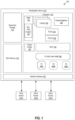
- FIG. 3 illustrates embodiments using a multi-key cryptographic memory protection system 300.
- memory protection system 300 includes processor 302, system agent 304, and memory 310. As described further below, memory protection system 300 provides cryptographic protection of data stored on memory 310.
- System agent 304 may be used to provide various functions for processor 302, such as managing access to memory 310 and/or other resources of system 300.
- system agent 304 includes a memory controller 308 to control and/or manage access to memory 310 of system 300.
- system agent 304 also includes a MKTME engine 145 to protect data stored on memory 310.
- system agent 304 may also provide an interface between processor 302 and other components of system 300 (e.g., using a direct media interface (DMI) and/or PCI-Express bridge).
- DMI direct media interface
- PCI-Express bridge PCI-Express bridge
- MKTME engine 145 may be implemented using any combination of hardware and/or software logic, including a microprocessor, application-specific integrated circuit (ASIC), field-programmable gate array (FPGA), programmable logic array (PLA), virtual machine (VM), and/or any other type of circuitry or logic.
- ASIC application-specific integrated circuit
- FPGA field-programmable gate array
- PDA programmable logic array
- VM virtual machine
- MKTME engine 145 uses memory encryption to protect data stored on memory 310.
- MKTME engine 145 may be implemented on the memory path or memory bus to allow encryption of data transmitted to and from, and/or stored on, memory 310.
- MKTME engine 145 may be configurable or programmable, and may include support for multiple encryption keys. Accordingly, MKTME engine 145 may be configured or programmed (e.g., by software) to encrypt different regions or pages of memory 310 using different encryption keys and/or algorithms. In this manner, memory encryption can be provided and configured separately for different users, tenants, customers, applications, and/or workloads.
- the MKTME engine 145 stores one or more keys 306.
- MKTME engine 145 may be used to define various secured or protected domains that can be separately configured and protected using memory encryption.
- a "domain" may be viewed as a collection of resources associated with a particular workload (e.g., a workload of a particular user or application), and may include any regions of memory containing data associated with the workload.
- a protected domain for a customer workload of a cloud service provider may include resources (e.g., memory) associated with an operating system (O/S), virtual machine (VM) (e.g., a VM running on a virtual machine manager (VMM)), and/or any ring-3 applications running on the O/S or VM.
- O/S operating system
- VM virtual machine
- VMM virtual machine manager
- MKTME engine 145 may allow the protected domains to be configured and protected separately, thus allowing each protected domain to be cryptographically isolated in memory by encrypting its associated code and/or data with a unique encryption key. In this manner, the workloads of different users, customers, and/or tenants can be cryptographically isolated by defining different protection domains for the various workloads.
- the cryptographic memory protection of system 300 may be discovered and configured using processor instructions and/or hardware registers.
- a processor instruction may be used to determine whether cryptographic memory protection is supported by system 300, such as a CPU identification (CPUID) instruction used by software to identify the capabilities of a particular processor.
- CPU identification CPUID
- control registers 303 may include various model-specific registers (MSRs) that allow software to discover, enable, and/or configure the cryptographic memory protection capabilities of system 300.
- MSRs model-specific registers
- control registers 303 may include a memory encryption capability register, a memory encryption activation register, and/or one or more memory encryption exclusion registers, as described further below.
- the memory encryption capability register may be used to allow software to discover the memory encryption capabilities of system 300.
- software can read the ME_CAPABILITY_MSR (e.g., using a read MSR (RDMSR) instruction) to identify the supported encryption types and/or algorithms, the maximum number of encryption keys that can be used concurrently, and so forth.
- RMSR read MSR
- the table below illustrates an example embodiment of the memory encryption capability register (ME_CAPABILITY_MSR).
- ME_CAPABILITY_MSR Memory Encryption Capability Register
- FIELD BIT INDEX DESCRIPTION SUPPORTED ENCRYPTION ALGORITHMS 0:15 This field is used to identify supported encryption algorithms or encryption types. Each bit of this field (if used) corresponds to a particular encryption algorithm. For example, bit 0 may correspond to AES-XTS 128-bit encryption, bit 1 may correspond to AES-XTS 256-bit encryption, and so forth. A particular encryption algorithm is supported if the corresponding bit has a value of 1, and is unsupported if the corresponding bit has a value of 0. RESERVED 16:31 These bits are unused and/or reserved (e.g., reserved for functionality extensions and/or other purposes).
- MAX # OF KEY ID BITS (ME_MAX_KEYID_BITS) 32:35
- the value of this field is 0 if multi-key memory encryption is not supported.
- the memory encryption activation register (ME_ACTIVATE_MSR) may be used to activate the cryptographic memory protection of system 300 (e.g., by setting the appropriate values in the register fields).
- the table below illustrates an example embodiment of the memory encryption activation register (ME_ACTIVATE_MSR).
- ME_ACTIVATE_MSR Memory Encryption Activation Register
- FIELD BIT INDEX DESCRIPTION READ-ONLY LOCK 0 This field is used to activate a read-only lock on the memory encryption configuration registers after memory encryption has been activated.
- the lock may be activated after memory encryption has been activated through a write to the ME_ACTIVATE_MSR register (e.g., using a write MSR or WRMSR instruction).
- the lock can be enabled by setting this bit field to 1, and the lock can be disabled by setting this bit field to 0.
- the lock is applied to the ME_ACTIVATE_MSR, ME_EXCLUDE_BASE_MSR, and ME_EXCLUDE_MASK_MSR registers. Any writes to these registers will be ignored while the lock is active.
- the lock is reset when the processor is reset.
- ENABLE MEMORY ENCRYPTION 1 This field is used to enable or disable memory encryption. Memory encryption is enabled when this bit field has a value of 1, and is disabled when this bit field has a value of 0.
- KEY SELECTION FOR DEFAULT MODE 2 This field is used to select a key to be used for default encryption mode. Memory regions protected using default encryption mode, for example, are protected uniformly using a default encryption algorithm and key. If this bit field is set to 0, a new key is created (e.g., after a cold or warm boot). If this bit field is set to 1, an existing key is restored from storage (e.g., after resuming from standby).
- SAVE KEY FOR STANDBY 3 This field is used to specify whether the key used for default encryption mode should be saved in order to allow the key to be restored after resuming from standby. If this bit field is set to 1, the key is saved. If this bit field is set to 0, the key is not saved. ENCRYPTION ALGORITHM FOR DEFAULT MODE 4:7 This field can be used to specify the encryption algorithm to use for default encryption mode. The value of this field identifies the bit index in the ME_CAPABILITY_MSR register that corresponds to the selected encryption algorithm. For example, the supported encryption algorithms are identified by bits 0:15 of the ME_CAPABILITY_MSR register.
- bit index 0 of the ME_CAPABILITY_MSR register may correspond to AES-XTS 128-bit encryption
- bit index 1 may correspond to AES-XTS 256-bit encryption
- bit index 0 (binary 0000)
- the encryption algorithm corresponding to bit index 0 of the ME_CAPABILITY_MSR register is selected, which would be AES-XTS 128-bit encryption.
- the present field has a value of 1 (binary 0001)
- the encryption algorithm corresponding to bit index 1 of the ME_CAPABILITY_MSR register is selected, which would be AES-XTS 256-bit encryption.
- the encryption algorithm selected using this field must be supported (e.g., its corresponding bit index in the ME_CAPABILITY_MSR register must be set to 1).
- RESERVED 8:31 These bits are unused and/or reserved (e.g., reserved for functionality extensions and/or other purposes).
- # OF KEY ID BITS (ME_KEYID_BITS) 32:35 This field is used to identify the number of bits that are used for KeylDentifiers. More specifically, the value of this field represents the number of higher order bits of a memory address that are used as a key or domain identifier for memory encryption.
- ENCRYPTION RESTRICTION BITMASK 48:63 This field can be used to restrict the encryption algorithms that can be used for multi-key encryption.
- the supported encryption algorithms are identified in the ME_CAPABILITY_MSR register (bits 0:15).
- the bits in the present field correspond to the bits of the ME_CAPABILITY_MSR register that are used to identify the supported encryption algorithms. In this manner, a supported encryption algorithm can be restricted from being used for multi-key encryption by clearing the corresponding bit in the present field (or alternatively, setting the corresponding bit).
- the memory encryption exclusion registers may be used to exclude certain memory regions from the cryptographic memory protection provided by system 300.
- the exclusion registers may be used to identify a base memory address, and memory encryption may then be bypassed for memory addresses matching the base address (e.g., allowing the excluded or bypassed memory addresses to be accessed in plaintext mode).
- the table below illustrates an example embodiment of the memory encryption exclusion mask register (ME_EXCLUDE_MASK_MSR), and the following table illustrates an example embodiment of the memory encryption exclusion base register (ME_EXCLUDE_BASE_MSR).
- ME_EXCLUDE_MASK_MSR Memory Encryption Exclusion Mask Register
- FIELD BIT INDEX DESCRIPTION RESERVED 0:10 These bits are unused and/or reserved (e.g., reserved for functionality extensions and/or other purposes).
- ENABLE EXCLUSION 11 This field can be used to enable or disable exclusions from memory encryption protection. When this field is set to 0, no memory addresses are excluded from memory encryption protection. When this field is set to 1, the ME_EXCLUDE_MASK_MSR and ME_EXCLUDE_BASE_MSR registers are used to define a memory range that is excluded from memory encryption protection.
- EXCLUSION MASK 12 (MAX ADDRESS SIZE-1) This field is used to identify the bits of a memory address that must match the EXCLUSION BASE (defined in the ME_EXCLUDE_BASE_MSR register) in order to qualify as an excluded memory range. For example, when accessing a particular memory address, the memory address can be AND-ed with the EXCLUSION MASK, and if the result matches the EXCLUSION BASE, memory encryption is bypassed for that memory address.
- RESERVED (MAX ADDRESS SIZE):63 These bits are unused and/or reserved (e.g., reserved for functionality extensions and/or other purposes).
- ME_EXCLUDE_BASE_MSR Memory Encryption Exclusion Base Register
- FIELD BIT INDEX DESCRIPTION RESERVED 0:11 These bits are unused and/or reserved (e.g., reserved for functionality extensions and/or other purposes).
- EXCLUSION BASE 12:(MAX ADDRESS SIZE-1) This field is used to identify the base memory address of a particular memory range to exclude from memory encryption protection.
- RESERVED (MAX ADDRESS SIZE):63 These bits are unused and/or reserved (e.g., reserved for functionality extensions and/or other purposes).
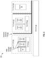
- MKTME engine 145 maintains an internal domain key table 307 to identify protected domains that have been configured in system 300.
- the key table 307 may be implemented using any form of memory or storage (e.g., RAM), and may also be implemented directly on MKTME engine 145, in memory 310, and/or using another memory component. Note that a "table” does not need to be used (other data structures may work), however, for ease of understanding a table is used in this description.
- the MKTME engine 145 includes a cryptographic unit 305 to use, or construct a tweak to be used in encryption/decryption.
- the MKTME engine 145 is arranged to use the tweak and a common key set to decrypt data specified by the read request with the encrypted memory address.
- the common key set is a single set of keys used by the without regard to which of several tenants or tenant workloads is being encrypted or decrypted. For example, workload data for a first tenant is encrypted using the same key from the common key set as workload data for a second tenant. The difference between the encryption of these workloads is in the tenant, or domain, specific tweaks created from the tenant specific keyid-nonces from KeylD registration.
- the decryption is accomplished by performing Advanced Encryption Standard (AES) XEX-based tweaked-codebook mode with ciphertext stealing (XTS) (AES-XTS) decryption, where the AES-XTS keys K1 and K2 are in the common key set (e.g., the same K1 and K2 are used for all tenant workloads) and the tweak is unique across mutually distrusting domains.
- AES Advanced Encryption Standard
- AES-XTS XEX-based tweaked-codebook mode with ciphertext stealing
- K1 and K2 are domain-specific keys.
- K1 and K2 are from the common key set and not domain specific keys, but the tweak is specific to the domains.
- a similar set of techniques as those described above to read encrypted data from memory are used to encrypt data to store in memory.
- the system agent is arranged to receive a write request for the encrypted memory.
- the write request includes the encrypted memory address.
- the system agent retrieves the KeyID-nonce from the key table 307 using the KeyID bits and constructs the tweak from the KeyID-nonce, the KeyID bits, and the physical address bits.
- the tweak in conjunction with the common key set, are then used to encrypt data specified by the write request.
- the encrypted data may then be stored in the memory at the physical address in the encrypted memory address.
- each entry 307a-d of domain key table 307 each correspond to a different protected domain.
- each entry 307a-d includes a key or domain identifier (ID), a protection mode, and an associated encryption key (if applicable).
- a KeyID may represent the higher order bits of the memory addresses that are within the associated protected domain.
- the ME_KEYID_BITS field of the ME_ACTIVATE_MSR register specifies the number of bits used for KeylDs.
- each KeylD in domain key table 307 is represented using 5 bits. Accordingly, the protected domain associated with a given KeylD covers all memory addresses whose highest order 5 bits match the KeyID.
- the KeyID is stored as a field in key table 307, but in alternative embodiments, the KeyID may be used as an index into key table 307 rather than being stored directly in key table 307.
- multiple protection modes may be supported, and each protected domain may be protected using a particular protection mode.
- the supported protection modes may include plaintext mode (e.g., unencrypted), standard or default encryption mode (e.g., encrypted using a standard or default encryption key), and/or custom encryption mode (e.g., encrypted using a unique encryption key).
- key table 307 may identify the protection mode associated with each protected domain or KeylD.
- domain key table 307 includes four entries.
- the first entry identifies a protected domain corresponding to KeyID 00000 (thus covering all memory addresses that contain 00000 in the highest order 5 bits), which is protected in default encryption mode using key "ABC.”
- the second entry identifies a protected domain corresponding to KeyID 00001 (thus covering all memory addresses that contain 00001 in the highest order 5 bits), which is protected in plaintext mode and thus does not have an associated encryption key.
- the third entry identifies a protected domain corresponding to KeyID 00010 (thus covering all memory addresses that contain 00010 in the highest order 5 bits), which is protected in custom encryption mode using key "XYZ.”
- the fourth entry identifies a protected domain corresponding to KeyID 00011 (thus covering all memory addresses that contain 00011 in the highest order 5 bits), which is protected in default encryption mode using key "ABC.”
- the domain protected using custom encryption mode has a unique key (“XYZ”), the domains protected using default encryption mode share an encryption key
- PCU 1017 may include a variety of power management logic units (circuitry) to perform hardware-based power management.
- Such power management may be wholly processor controlled (e.g., by various processor hardware, and which may be triggered by workload and/or power, thermal or other processor constraints) and/or the power management may be performed responsive to external sources (such as a platform or power management source or system software).
- PCU 1017 is illustrated as being present as logic separate from the processor 1070 and/or processor 1080. In other cases, PCU 1017 may execute on a given one or more of cores (not shown) of processor 1070 or 1080. In some cases, PCU 1017 may be implemented as a microcontroller (dedicated or general-purpose) or other control logic configured to execute its own dedicated power management code, sometimes referred to as P-code. In yet other embodiments, power management operations to be performed by PCU 1017 may be implemented externally to a processor, such as by way of a separate power management integrated circuit (PMIC) or another component external to the processor. In yet other embodiments, power management operations to be performed by PCU 1017 may be implemented within BIOS or other system software.
- PMIC power management integrated circuit
- Various I/O devices 1014 may be coupled to first interconnect 1016, along with an interconnect (bus) bridge 1018 which couples first interconnect 1016 to a second interconnect 1020.
- one or more additional processor(s) 1015 such as coprocessors, high-throughput MIC processors, GPGPU's, accelerators (such as, e.g., graphics accelerators or digital signal processing (DSP) units), field programmable gate arrays (FPGAs), or any other processor, are coupled to first interconnect 1016.
- second interconnect 1020 may be a low pin count (LPC) interconnect.
- LPC low pin count
- the processor 1100 may be a general-purpose processor, coprocessor or special-purpose processor, such as, for example, a network or communication processor, compression engine, graphics processor, GPGPU (general purpose graphics processing unit circuitry), a high-throughput many integrated core (MIC) coprocessor (including 30 or more cores), embedded processor, or the like.
- the processor may be implemented on one or more chips.
- the processor 1100 may be a part of and/or may be implemented on one or more substrates using any of a number of process technologies, such as, for example, BiCMOS, CMOS, or NMOS.
- a memory hierarchy includes one or more levels of cache unit(s) circuitry 1104(A)-(N) within the cores 1102(A)-(N), a set of one or more shared cache units circuitry 1106, and external memory (not shown) coupled to the set of integrated memory controller units circuitry 1114.
- the set of one or more shared cache units circuitry 1106 may include one or more mid-level caches, such as level 2 (L2), level 3 (L3), level 4 (L4), or other levels of cache, such as a last level cache (LLC), and/or combinations thereof.
- LLC last level cache
- ring- based interconnect network circuitry 1112 interconnects the special purpose logic 1108 (e.g., integrated graphics logic), the set of shared cache units circuitry 1106, and the system agent unit circuitry 1110
- special purpose logic 1108 e.g., integrated graphics logic
- the set of shared cache units circuitry 1106, and the system agent unit circuitry 1110 alternative embodiments use any number of well-known techniques for interconnecting such units.
- coherency is maintained between one or more of the shared cache units circuitry 1106 and cores 1102(A)-(N).
- the system agent unit circuitry 1110 includes those components coordinating and operating cores 1102(A)-(N).
- the system agent unit circuitry 1110 may include, for example, power control unit (PCU) circuitry and/or display unit circuitry (not shown).
- the PCU may be or may include logic and components needed for regulating the power state of the cores 1102(A)-(N) and/or the special purpose logic 1108 (e.g., integrated graphics logic).
- the display unit circuitry is for driving one or more externally connected displays.
- the cores 1102(A)-(N) may be homogenous or heterogeneous in terms of architecture instruction set; that is, two or more of the cores 1102(A)-(N) may be capable of executing the same instruction set, while other cores may be capable of executing only a subset of that instruction set or a different instruction set.
- FIG. 12(A) is a block diagram illustrating both an exemplary in-order pipeline and an exemplary register renaming, out-of-order issue/execution pipeline according to embodiments of the invention.
- FIG. 12(B) is a block diagram illustrating both an exemplary embodiment of an in-order architecture core and an exemplary register renaming, out-of-order issue/execution architecture core to be included in a processor according to embodiments of the invention.
- the solid lined boxes in FIGS. 12(A)-(B) illustrate the in-order pipeline and in-order core, while the optional addition of the dashed lined boxes illustrates the register renaming, out-of-order issue/execution pipeline and core. Given that the in-order aspect is a subset of the out-of-order aspect, the out-of-order aspect will be described.
- a processor pipeline 1200 includes a fetch stage 1202, an optional length decode stage 1204, a decode stage 1206, an optional allocation stage 1208, an optional renaming stage 1210, a scheduling (also known as a dispatch or issue) stage 1212, an optional register read/memory read stage 1214, an execute stage 1216, a write back/memory write stage 1218, an optional exception handling stage 1222, and an optional commit stage 1224.
- a fetch stage 1202 an optional length decode stage 1204, a decode stage 1206, an optional allocation stage 1208, an optional renaming stage 1210, a scheduling (also known as a dispatch or issue) stage 1212, an optional register read/memory read stage 1214, an execute stage 1216, a write back/memory write stage 1218, an optional exception handling stage 1222, and an optional commit stage 1224.
- a scheduling also known as a dispatch or issue
- one or more instructions are fetched from instruction memory
- the one or more fetched instructions may be decoded, addresses (e.g., load store unit (LSU) addresses) using forwarded register ports may be generated, and branch forwarding (e.g., immediate offset or an link register (LR)) may be performed.
- LSU load store unit
- LR link register
- the decode stage 1206 and the register read/memory read stage 1214 may be combined into one pipeline stage.
- the decoded instructions may be executed, LSU address/data pipelining to an Advanced Microcontroller Bus (AHB) interface may be performed, multiply and add operations may be performed, arithmetic operations with branch results may be performed, etc.
- APB Advanced Microcontroller Bus
- the exemplary register renaming, out-of-order issue/execution core architecture may implement the pipeline 1200 as follows: 1) the instruction fetch 1238 performs the fetch and length decoding stages 1202 and 1204; 2) the decode unit circuitry 1240 performs the decode stage 1206; 3) the rename/allocator unit circuitry 1252 performs the allocation stage 1208 and renaming stage 1210; 4) the scheduler unit(s) circuitry 1256 performs the schedule stage 1212; 5) the physical register file(s) unit(s) circuitry 1258 and the memory unit circuitry 1270 perform the register read/memory read stage 1214; the execution cluster 1260 perform the execute stage 1216; 6) the memory unit circuitry 1270 and the physical register file(s) unit(s) circuitry 1258 perform the write back/memory write stage 1218; 7) various units (unit circuitry) may be involved in the exception handling stage 1222; and 8) the retirement unit circuitry 1254 and the physical register file(s) unit(s) circuit
- FIG. 12(B) shows processor core 1290 including front-end unit circuitry 1230 coupled to an execution engine unit circuitry 1250, and both are coupled to a memory unit circuitry 1270.
- the core 1290 may be a reduced instruction set computing (RISC) core, a complex instruction set computing (CISC) core, a very long instruction word (VLIW) core, or a hybrid or alternative core type.
- the core 1290 may be a special-purpose core, such as, for example, a network or communication core, compression engine, coprocessor core, general purpose computing graphics processing unit (GPGPU) core, graphics core, or the like.
- GPGPU general purpose computing graphics processing unit
- the front end unit circuitry 1230 may include branch prediction unit circuitry 1232 coupled to an instruction cache unit circuitry 1234, which is coupled to an instruction translation lookaside buffer (TLB) 1236, which is coupled to instruction fetch unit circuitry 1238, which is coupled to decode unit circuitry 1240.
- the instruction cache unit circuitry 1234 is included in the memory unit circuitry 1270 rather than the front-end unit circuitry 1230.
- the decode unit circuitry 1240 (or decoder) may decode instructions, and generate as an output one or more micro-operations, micro-code entry points, microinstructions, other instructions, or other control signals, which are decoded from, or which otherwise reflect, or are derived from, the original instructions.
- the decode unit circuitry 1240 may further include an address generation unit circuitry (AGU, not shown).
- AGU address generation unit circuitry
- the AGU generates an LSU address using forwarded register ports, and may further perform branch forwarding (e.g., immediate offset branch forwarding, LR register branch forwarding, etc.).
- the decode unit circuitry 1240 may be implemented using various different mechanisms. Examples of suitable mechanisms include, but are not limited to, look-up tables, hardware implementations, programmable logic arrays (PLAs), microcode read only memories (ROMs), etc.
- the core 1290 includes a microcode ROM (not shown) or other medium that stores microcode for certain macroinstructions (e.g., in decode unit circuitry 1240 or otherwise within the front end unit circuitry 1230).
- the decode unit circuitry 1240 includes a micro-operation (micro-op) or operation cache (not shown) to hold/cache decoded operations, micro-tags, or micro-operations generated during the decode or other stages of the processor pipeline 1200.
- the decode unit circuitry 1240 may be coupled to rename/allocator unit circuitry 1252 in the execution engine unit circuitry 1250.
- the execution engine circuitry 1250 includes the rename/allocator unit circuitry 1252 coupled to a retirement unit circuitry 1254 and a set of one or more scheduler(s) circuitry 1256.
- the scheduler(s) circuitry 1256 represents any number of different schedulers, including reservations stations, central instruction window, etc.
- the scheduler(s) circuitry 1256 can include arithmetic logic unit (ALU) scheduler/scheduling circuitry, ALU queues, arithmetic generation unit (AGU) scheduler/scheduling circuitry, AGU queues, etc.
- ALU arithmetic logic unit
- AGU arithmetic generation unit
- the scheduler(s) circuitry 1256 is coupled to the physical register file(s) circuitry 1258.
- Each of the physical register file(s) circuitry 1258 represents one or more physical register files, different ones of which store one or more different data types, such as scalar integer, scalar floating-point, packed integer, packed floating-point, vector integer, vector floating-point, status (e.g., an instruction pointer that is the address of the next instruction to be executed), etc.
- the physical register file(s) unit circuitry 1258 includes vector registers unit circuitry, writemask registers unit circuitry, and scalar register unit circuitry. These register units may provide architectural vector registers, vector mask registers, general-purpose registers, etc.
- the physical register file(s) unit(s) circuitry 1258 is overlapped by the retirement unit circuitry 1254 (also known as a retire queue or a retirement queue) to illustrate various ways in which register renaming and out-of-order execution may be implemented (e.g., using a reorder buffer(s) (ROB(s)) and a retirement register file(s); using a future file(s), a history buffer(s), and a retirement register file(s); using a register maps and a pool of registers; etc.).
- the retirement unit circuitry 1254 and the physical register file(s) circuitry 1258 are coupled to the execution cluster(s) 1260.
- the execution cluster(s) 1260 includes a set of one or more execution units circuitry 1262 and a set of one or more memory access circuitry 1264.
- the execution units circuitry 1262 may perform various arithmetic, logic, floating-point or other types of operations (e.g., shifts, addition, subtraction, multiplication) and on various types of data (e.g., scalar floating-point, packed integer, packed floating-point, vector integer, vector floating-point). While some embodiments may include a number of execution units or execution unit circuitry dedicated to specific functions or sets of functions, other embodiments may include only one execution unit circuitry or multiple execution units/execution unit circuitry that all perform all functions.
- the scheduler(s) circuitry 1256, physical register file(s) unit(s) circuitry 1258, and execution cluster(s) 1260 are shown as being possibly plural because certain embodiments create separate pipelines for certain types of data/operations (e.g., a scalar integer pipeline, a scalar floating-point/packed integer/packed floating-point/vector integer/vector floating-point pipeline, and/or a memory access pipeline that each have their own scheduler circuitry, physical register file(s) unit circuitry, and/or execution cluster - and in the case of a separate memory access pipeline, certain embodiments are implemented in which only the execution cluster of this pipeline has the memory access unit(s) circuitry 1264). It should also be understood that where separate pipelines are used, one or more of these pipelines may be out-of-order issue/execution and the rest in-order.
- the execution engine unit circuitry 1250 may perform load store unit (LSU) address/data pipelining to an Advanced Microcontroller Bus (AHB) interface (not shown), and address phase and writeback, data phase load, store, and branches.
- LSU load store unit
- AHB Advanced Microcontroller Bus
- the set of memory access circuitry 1264 is coupled to the memory unit circuitry 1270, which includes data TLB unit circuitry 1272 coupled to a data cache circuitry 1274 coupled to a level 2 (L2) cache circuitry 1276.
- the memory access units circuitry 1264 may include a load unit circuitry, a store address unit circuit, and a store data unit circuitry, each of which is coupled to the data TLB circuitry 1272 in the memory unit circuitry 1270.
- the instruction cache circuitry 1234 is further coupled to a level 2 (L2) cache unit circuitry 1276 in the memory unit circuitry 1270.
- the instruction cache 1234 and the data cache 1274 are combined into a single instruction and data cache (not shown) in L2 cache unit circuitry 1276, a level 3 (L3) cache unit circuitry (not shown), and/or main memory.
- L2 cache unit circuitry 1276 is coupled to one or more other levels of cache and eventually to a main memory.
- the core 1290 may support one or more instructions sets (e.g., the x86 instruction set (with some extensions that have been added with newer versions); the MIPS instruction set; the ARM instruction set (with optional additional extensions such as NEON)), including the instruction(s) described herein.
- the core 1290 includes logic to support a packed data instruction set extension (e.g., AVX1, AVX2), thereby allowing the operations used by many multimedia applications to be performed using packed data.
- a packed data instruction set extension e.g., AVX1, AVX2
- FIG. 13 illustrates embodiments of execution unit(s) circuitry, such as execution unit(s) circuitry 1262 of FIG. 12(B) .
- execution unit(s) circuity 1262 may include one or more ALU circuits 1301, vector/SIMD unit circuits 1303, load/store unit circuits 1305, and/or branch/jump unit circuits 1307.
- ALU circuits 1301 perform integer arithmetic and/or Boolean operations.
- Vector/SIMD unit circuits 1303 perform vector/SIMD operations on packed data (such as SIMD/vector registers).
- Load/store unit circuits 1305 execute load and store instructions to load data from memory into registers or store from registers to memory. Load/store unit circuits 1305 may also generate addresses.
- Branch/jump unit circuits 1307 cause a branch or jump to a memory address depending on the instruction.
- Floating-point unit (FPU) circuits 1309 perform floating-point arithmetic.
- the width of the execution unit(s) circuitry 1262 varies depending upon the embodiment and can range from 16-bit to 1,024-bit. In some embodiments, two or more smaller execution units are logically combined to form a larger execution unit (e.g., two 128-bit execution units are logically combined to form a 256-bit execution unit).
- FIG. 14 is a block diagram of a register architecture 1400 according to some embodiments. As illustrated, there are vector/SIMD registers 1410 that vary from 128-bit to 1,024 bits width. In some embodiments, the vector/SIMD registers 1410 are physically 512-bits and, depending upon the mapping, only some of the lower bits are used. For example, in some embodiments, the vector/SIMD registers 1410 are ZMM registers which are 512 bits: the lower 256 bits are used for YMM registers and the lower 128 bits are used for XMM registers. As such, there is an overlay of registers.
- a vector length field selects between a maximum length and one or more other shorter lengths, where each such shorter length is half the length of the preceding length.
- Scalar operations are operations performed on the lowest order data element position in a ZMM/YMM/XMM register; the higher order data element positions are either left the same as they were prior to the instruction or zeroed depending on the embodiment.
- the register architecture 1400 includes writemask/predicate registers 1415.
- writemask/predicate registers 1415 there are 8 writemask/predicate registers (sometimes called k0 through k7) that are each 16-bit, 32-bit, 64-bit, or 128-bit in size.
- Writemask/predicate registers 1415 may allow for merging (e.g., allowing any set of elements in the destination to be protected from updates during the execution of any operation) and/or zeroing (e.g., zeroing vector masks allow any set of elements in the destination to be zeroed during the execution of any operation).
- each data element position in a given writemask/predicate register 1415 corresponds to a data element position of the destination.
- the writemask/predicate registers 1415 are scalable and consists of a set number of enable bits for a given vector element (e.g., 8 enable bits per 64-bit vector element).
- the register architecture 1400 includes a plurality of general-purpose registers 1425. These registers may be 16-bit, 32-bit, 64-bit, etc. and can be used for scalar operations. In some embodiments, these registers are referenced by the names RAX, RBX, RCX, RDX, RBP, RSI, RDI, RSP, and R8 through R15.
- the register architecture 1400 includes scalar floating-point register 1445 which is used for scalar floating-point operations on 32/64/80-bit floating-point data using the x87 instruction set extension or as MMX registers to perform operations on 64-bit packed integer data, as well as to hold operands for some operations performed between the MMX and XMM registers.
- One or more flag registers 1440 store status and control information for arithmetic, compare, and system operations.
- the one or more flag registers 1440 may store condition code information such as carry, parity, auxiliary carry, zero, sign, and overflow.
- the one or more flag registers 1440 are called program status and control registers.
- Segment registers 1420 contain segment points for use in accessing memory. In some embodiments, these registers are referenced by the names CS, DS, SS, ES, FS, and GS.
- Machine specific registers (MSRs) 1435 control and report on processor performance. Most MSRs 1435 handle system-related functions and are not accessible to an application program. Machine check registers 1460 consist of control, status, and error reporting MSRs that are used to detect and report on hardware errors.
- One or more instruction pointer register(s) 1430 store an instruction pointer value.
- Control register(s) 1455 e.g., CR0-CR4
- determine the operating mode of a processor e.g., processor 1070, 1080, 1038, 1015, and/or 1100
- Debug registers 1450 control and allow for the monitoring of a processor or core's debugging operations.
- Memory management registers 1465 specify the locations of data structures used in protected mode memory management. These registers may include a GDTR, IDRT, task register, and a LDTR register.
- Alternative embodiments of the invention may use wider or narrower registers. Additionally, alternative embodiments of the invention may use more, less, or different register files and registers.
- An instruction set architecture may include one or more instruction formats.
- a given instruction format may define various fields (e.g., number of bits, location of bits) to specify, among other things, the operation to be performed (e.g., opcode) and the operand(s) on which that operation is to be performed and/or other data field(s) (e.g., mask).
- Some instruction formats are further broken down though the definition of instruction templates (or sub-formats).
- the instruction templates of a given instruction format may be defined to have different subsets of the instruction format's fields (the included fields are typically in the same order, but at least some have different bit positions because there are less fields included) and/or defined to have a given field interpreted differently.
- each instruction of an ISA is expressed using a given instruction format (and, if defined, in a given one of the instruction templates of that instruction format) and includes fields for specifying the operation and the operands.
- an exemplary ADD instruction has a specific opcode and an instruction format that includes an opcode field to specify that opcode and operand fields to select operands (source1/destination and source2); and an occurrence of this ADD instruction in an instruction stream will have specific contents in the operand fields that select specific operands.
- Embodiments of the instruction(s) described herein may be embodied in different formats. Additionally, exemplary systems, architectures, and pipelines are detailed below. Embodiments of the instruction(s) may be executed on such systems, architectures, and pipelines, but are not limited to those detailed.
- the prefix(es) field(s) 1501 when used, modifies an instruction.
- one or more prefixes are used to repeat string instructions (e.g., 0xF0, 0xF2, 0xF3, etc.), to provide section overrides (e.g., 0x2E, 0x36, 0x3E, 0x26, 0x64, 0x65, 0x2E, 0x3E, etc.), to perform bus lock operations, and/or to change operand (e.g., 0x66) and address sizes (e.g., 0x67).
- Certain instructions require a mandatory prefix (e.g., 0x66, 0xF2, 0xF3, etc.). Certain of these prefixes may be considered “legacy" prefixes. Other prefixes, one or more examples of which are detailed herein, indicate, and/or provide further capability, such as specifying particular registers, etc. The other prefixes typically follow the "legacy" prefixes.
- the opcode field 1503 is used to at least partially define the operation to be performed upon a decoding of the instruction.
- a primary opcode encoded in the opcode field 1503 is 1, 2, or 3 bytes in length. In other embodiments, a primary opcode can be a different length. An additional 3-bit opcode field is sometimes encoded in another field.
- the addressing field 1505 is used to address one or more operands of the instruction, such as a location in memory or one or more registers.
- FIG. 16 illustrates embodiments of the addressing field 1505.
- an optional ModR/M byte 1602 and an optional Scale, Index, Base (SIB) byte 1604 are shown.
- the ModR/M byte 1602 and the SIB byte 1604 are used to encode up to two operands of an instruction, each of which is a direct register or effective memory address. Note that each of these fields are optional in that not all instructions include one or more of these fields.
- the MOD R/M byte 1602 includes a MOD field 1642, a register field 1644, and R/M field 1646.
- the content of the MOD field 1642 distinguishes between memory access and non-memory access modes.
- a register-direct addressing mode is utilized, and otherwise register-indirect addressing is used.
- the R/M field 1646 may be used to encode an instruction operand that references a memory address, or may be used to encode either the destination register operand or a source register operand. Note the R/M field 1646 may be combined with the MOD field 1642 to dictate an addressing mode in some embodiments.
- the SIB byte 1604 includes a scale field 1652, an index field 1654, and a base field 1656 to be used in the generation of an address.
- the scale field 1652 indicates scaling factor.
- the index field 1654 specifies an index register to use. In some embodiments, the index field 1654 is supplemented with an additional bit from a prefix (e.g., prefix 1501) to allow for greater addressing.
- the base field 1656 specifies a base register to use. In some embodiments, the base field 1656 is supplemented with an additional bit from a prefix (e.g., prefix 1501) to allow for greater addressing.
- the content of the scale field 1652 allows for the scaling of the content of the index field 1654 for memory address generation (e.g., for address generation that uses 2 scale * index + base).
- a memory address may be generated according to 2 scale * index + base + displacement, index*scale+displacement, r/m + displacement, instruction pointer (RIP/EIP) + displacement, register + displacement, etc.
- the displacement may be a 1-byte, 2-byte, 4-byte, etc. value.
- a displacement field 1507 provides this value.
- a displacement factor usage is encoded in the MOD field of the addressing field 1505 that indicates a compressed displacement scheme for which a displacement value is calculated by multiplying disp8 in conjunction with a scaling factor N that is determined based on the vector length, the value of a b bit, and the input element size of the instruction.
- the displacement value is stored in the displacement field 1507.
- an immediate field 1509 specifies an immediate for the instruction.
- An immediate may be encoded as a 1-byte value, a 2-byte value, a 4-byte value, etc.
- FIG. 17 illustrates embodiments of a first prefix 1501(A).
- the first prefix 1501(A) is an embodiment of a REX prefix. Instructions that use this prefix may specify general purpose registers, 64-bit packed data registers (e.g., single instruction, multiple data (SIMD) registers or vector registers), and/or control registers and debug registers (e.g., CR8-CR15 and DR8-DR15).
- SIMD single instruction, multiple data
- Instructions using the first prefix 1501(A) may specify up to three registers using 3-bit fields depending on the format: 1) using the reg field 1644 and the R/M field 1646 of the Mod R/M byte 1602; 2) using the Mod R/M byte 1602 with the SIB byte 1604 including using the reg field 1644 and the base field 1656 and index field 1654; or 3) using the register field of an opcode.
- bit positions 7:4 are set as 0100.
- bit position 2 may an extension of the MOD R/M reg field 1644 and may be used to modify the ModR/M reg field 1644 when that field encodes a general purpose register, a 64-bit packed data register (e.g., a SSE register), or a control or debug register. R is ignored when Mod R/M byte 1602 specifies other registers or defines an extended opcode.
- Bit position 1 (X) X bit may modify the SIB byte index field 1654.
- Bit position B (B) B may modify the base in the Mod R/M R/M field 1646 or the SIB byte base field 1656; or it may modify the opcode register field used for accessing general purpose registers (e.g., general purpose registers 1425).
- FIGS. 18(A)-(D) illustrate embodiments of how the R, X, and B fields of the first prefix 1501(A) are used.
- FIG. 18(A) illustrates R and B from the first prefix 1501(A) being used to extend the reg field 1644 and R/M field 1646 of the MOD R/M byte 1602 when the SIB byte 1604 is not used for memory addressing.
- FIG. 18(B) illustrates R and B from the first prefix 1501(A) being used to extend the reg field 1644 and R/M field 1646 of the MOD R/M byte 1602 when the SIB byte 16 04 is not used (register-register addressing).
- FIG. 18(A) illustrates R and B from the first prefix 1501(A) being used to extend the reg field 1644 and R/M field 1646 of the MOD R/M byte 1602 when the SIB byte 16 04 is not used (register-register addressing).
- FIG. 18(A) illustrates R and B from the first pre
- FIG. 18(C) illustrates R, X, and B from the first prefix 1501(A) being used to extend the reg field 1644 of the MOD R/M byte 1602 and the index field 1654 and base field 1656 when the SIB byte 1604 being used for memory addressing.
- FIG. 18(D) illustrates B from the first prefix 1501(A) being used to extend the reg field 1644 of the MOD R/M byte 1602 when a register is encoded in the opcode 1503.
- FIGS. 19(A)-(B) illustrate embodiments of a second prefix 1501(B).
- the second prefix 1501(B) is an embodiment of a VEX prefix.
- the second prefix 1501(B) encoding allows instructions to have more than two operands, and allows SIMD vector registers (e.g., vector/SIMD registers 1410) to be longer than 64-bits (e.g., 128-bit and 256-bit).
- SIMD vector registers e.g., vector/SIMD registers 1410) to be longer than 64-bits (e.g., 128-bit and 256-bit).
- the second prefix 1501(B) comes in two forms - a two-byte form and a three-byte form.
- the two-byte second prefix 1501(B) is used mainly for 128-bit, scalar, and some 256-bit instructions; while the three-byte second prefix 1501(B) provides a compact replacement of the first prefix 1501(A) and 3-byte opcode instructions.
- FIG. 19(A) illustrates embodiments of a two-byte form of the second prefix 1501(B).
- a format field 1901 (byte 0 1903) contains the value C5H.
- byte 1 1905 includes a "R" value in bit[7]. This value is the complement of the same value of the first prefix 1501(A).
- Bit[2] is used to dictate the length (L) of the vector (where a value of 0 is a scalar or 128-bit vector and a value of 1 is a 256-bit vector).
- Bits[6:3] shown as vvvv may be used to: 1) encode the first source register operand, specified in inverted (1s complement) form and valid for instructions with 2 or more source operands; 2) encode the destination register operand, specified in 1s complement form for certain vector shifts; or 3) not encode any operand, the field is reserved and should contain a certain value, such as 1111b.
- Instructions that use this prefix may use the Mod R/M R/M field 1646 to encode the instruction operand that references a memory address or encode either the destination register operand or a source register operand.
- Instructions that use this prefix may use the Mod R/M reg field 1644 to encode either the destination register operand or a source register operand, be treated as an opcode extension and not used to encode any instruction operand.
- vvvv For instruction syntax that support four operands, vvvv, the Mod R/M R/M field 1646 and the Mod R/M reg field 1644 encode three of the four operands. Bits[7:4] of the immediate 1509 are then used to encode the third source register operand.
- FIG. 19(B) illustrates embodiments of a three-byte form of the second prefix 1501(B).
- a format field 1911 (byte 0 1913) contains the value C4H.
- Byte 11915 includes in bits[7:5] "R,” "X,” and "B” which are the complements of the same values of the first prefix 1501(A).
- Bits[4:0] of byte 11915 (shown as mmmmm) include content to encode, as need, one or more implied leading opcode bytes. For example, 00001 implies a 0FH leading opcode, 00010 implies a 0F38H leading opcode, 00011 implies a leading 0F3AH opcode, etc.
- Bit[7] of byte 2 1917 is used similar to W of the first prefix 1501(A) including helping to determine promotable operand sizes.
- Bit[2] is used to dictate the length (L) of the vector (where a value of 0 is a scalar or 128-bit vector and a value of 1 is a 256-bit vector).
- Bits[6:3], shown as vvvv may be used to: 1) encode the first source register operand, specified in inverted (1s complement) form and valid for instructions with 2 or more source operands; 2) encode the destination register operand, specified in 1s complement form for certain vector shifts; or 3) not encode any operand, the field is reserved and should contain a certain value, such as 1111b.
- Instructions that use this prefix may use the Mod R/M R/M field 1646 to encode the instruction operand that references a memory address or encode either the destination register operand or a source register operand.
- Instructions that use this prefix may use the Mod R/M reg field 1644 to encode either the destination register operand or a source register operand, be treated as an opcode extension and not used to encode any instruction operand.
- vvvv For instruction syntax that support four operands, vvvv, the Mod R/M R/M field 1646, and the Mod R/M reg field 1644 encode three of the four operands. Bits[7:4] of the immediate 1509 are then used to encode the third source register operand.
- FIG. 20 illustrates embodiments of a third prefix 1501(C).
- the first prefix 1501(A) is an embodiment of an EVEX prefix.
- the third prefix 1501(C) is a four-byte prefix.
- the third prefix 1501(C) can encode 32 vector registers (e.g., 128-bit, 256-bit, and 512-bit registers) in 64-bit mode.
- instructions that utilize a writemask/opmask see discussion of registers in a previous figure, such as FIG. 14 ) or predication utilize this prefix.
- Opmask register allow for conditional processing or selection control.
- Opmask instructions, whose source/destination operands are opmask registers and treat the content of an opmask register as a single value, are encoded using the second prefix 1501(B).
- the third prefix 1501(C) may encode functionality that is specific to instruction classes (e.g., a packed instruction with "load+op" semantic can support embedded broadcast functionality, a floating-point instruction with rounding semantic can support static rounding functionality, a floating-point instruction with non-rounding arithmetic semantic can support "suppress all exceptions" functionality, etc.).
- instruction classes e.g., a packed instruction with "load+op” semantic can support embedded broadcast functionality, a floating-point instruction with rounding semantic can support static rounding functionality, a floating-point instruction with non-rounding arithmetic semantic can support "suppress all exceptions" functionality, etc.
- the first byte of the third prefix 1501(C) is a format field 2011 that has a value, in one example, of 62H. Subsequent bytes are referred to as payload bytes 2015-2019 and collectively form a 24-bit value of P[23:0] providing specific capability in the form of one or more fields (detailed herein).
- P[1:0] of payload byte 2019 are identical to the low two mmmmm bits.
- P[3:2] are reserved in some embodiments.
- Bit P[4] (R') allows access to the high 16 vector register set when combined with P[7] and the ModR/M reg field 1644.
- P[6] can also provide access to a high 16 vector register when SIB-type addressing is not needed.
- P[7:5] consist of an R, X, and B which are operand specifier modifier bits for vector register, general purpose register, memory addressing and allow access to the next set of 8 registers beyond the low 8 registers when combined with the ModR/M register field 1644 and ModR/M R/M field 1646.
- P[10] in some embodiments is a fixed value of 1.
- P[14:11], shown as vvvv, may be used to: 1) encode the first source register operand, specified in inverted (1s complement) form and valid for instructions with 2 or more source operands; 2) encode the destination register operand, specified in 1s complement form for certain vector shifts; or 3) not encode any operand, the field is reserved and should contain a certain value, such as 1111b.
- P[15] is similar to W of the first prefix 1501(A) and second prefix 1511(B) and may serve as an opcode extension bit or operand size promotion.
- P[18:16] specify the index of a register in the opmask (writemask) registers (e.g., writemask/predicate registers 1415).
- vector masks allow any set of elements in the destination to be protected from updates during the execution of any operation (specified by the base operation and the augmentation operation); in other one embodiment, preserving the old value of each element of the destination where the corresponding mask bit has a 0.
- any set of elements in the destination when zeroing vector masks allow any set of elements in the destination to be zeroed during the execution of any operation (specified by the base operation and the augmentation operation); in one embodiment, an element of the destination is set to 0 when the corresponding mask bit has a 0 value.
- a subset of this functionality is the ability to control the vector length of the operation being performed (that is, the span of elements being modified, from the first to the last one); however, it is not necessary that the elements that are modified be consecutive.
- the opmask field allows for partial vector operations, including loads, stores, arithmetic, logical, etc.
- opmask field's content selects one of a number of opmask registers that contains the opmask to be used (and thus the opmask field's content indirectly identifies that masking to be performed)
- alternative embodiments instead or additional allow the mask write field's content to directly specify the masking to be performed.
- P[19] can be combined with P[14:11] to encode a second source vector register in a non-destructive source syntax which can access an upper 16 vector registers using P[19].
- P[20] encodes multiple functionalities, which differs across different classes of instructions and can affect the meaning of the vector length/ rounding control specifier field (P[22:21]).
- P[23] indicates support for merging-writemasking (e.g., when set to 0) or support for zeroing and merging-writemasking (e.g., when set to 1).
- Table 1 32-Register Support in 64-bit Mode 4 3 [2:0] REG. TYPE COMMON USAGES REG R' R ModR/M reg GPR, Vector Destination or Source VVVV V' vvv GPR, Vector 2nd Source or Destination RM X B ModR/M R/M GPR, Vector 1st Source or Destination BASE 0 B ModR/M R/M GPR Memory addressing INDEX 0 X SIB.index GPR Memory addressing VIDX V' X SIB.index Vector VSIB memory addressing Table 2: Encoding Register Specifiers in 32-bit Mode [2:0] REG.
- Program code may be applied to input instructions to perform the functions described herein and generate output information.
- the output information may be applied to one or more output devices, in known fashion.
- a processing system includes any system that has a processor, such as, for example, a digital signal processor (DSP), a microcontroller, an application specific integrated circuit (ASIC), or a microprocessor.
- DSP digital signal processor
- ASIC application specific integrated circuit
- the program code may be implemented in a high-level procedural or object-oriented programming language to communicate with a processing system.
- the program code may also be implemented in assembly or machine language, if desired.
- the mechanisms described herein are not limited in scope to any particular programming language. In any case, the language may be a compiled or interpreted language.
- Embodiments of the mechanisms disclosed herein may be implemented in hardware, software, firmware, or a combination of such implementation approaches.
- Embodiments of the invention may be implemented as computer programs or program code executing on programmable systems comprising at least one processor, a storage system (including volatile and non-volatile memory and/or storage elements), at least one input device, and at least one output device.
- IP cores may be stored on a tangible, machine readable medium and supplied to various customers or manufacturing facilities to load into the fabrication machines that actually make the logic or processor.
- Such machine-readable storage media may include, without limitation, non-transitory, tangible arrangements of articles manufactured or formed by a machine or device, including storage media such as hard disks, any other type of disk including floppy disks, optical disks, compact disk read-only memories (CD-ROMs), compact disk rewritable's (CD-RWs), and magneto-optical disks, semiconductor devices such as read-only memories (ROMs), random access memories (RAMs) such as dynamic random access memories (DRAMs), static random access memories (SRAMs), erasable programmable read-only memories (EPROMs), flash memories, electrically erasable programmable read-only memories (EEPROMs), phase change memory (PCM), magnetic or optical cards, or any other type of media suitable for storing electronic instructions.
- storage media such as hard disks, any other type of disk including floppy disks, optical disks, compact disk read-only memories (CD-ROMs), compact disk rewritable's (CD-RWs), and magneto
- embodiments of the invention also include non-transitory, tangible machine-readable media containing instructions or containing design data, such as Hardware Description Language (HDL), which defines structures, circuits, apparatuses, processors and/or system features described herein.
- HDL Hardware Description Language
- Such embodiments may also be referred to as program products.
- Emulation including binary translation, code morphing, etc.
- an instruction converter may be used to convert an instruction from a source instruction set to a target instruction set.
- the instruction converter may translate (e.g., using static binary translation, dynamic binary translation including dynamic compilation), morph, emulate, or otherwise convert an instruction to one or more other instructions to be processed by the core.
- the instruction converter may be implemented in software, hardware, firmware, or a combination thereof.
- the instruction converter may be on processor, off processor, or part on and part off processor.
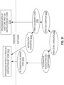
- FIG. 21 illustrates a block diagram contrasting the use of a software instruction converter to convert binary instructions in a source instruction set to binary instructions in a target instruction set according to embodiments of the invention.
- the instruction converter is a software instruction converter, although alternatively the instruction converter may be implemented in software, firmware, hardware, or various combinations thereof.
- FIG. 21 shows a program in a high level language 2102 may be compiled using a first ISA compiler 2104 to generate first ISA binary code 2106 that may be natively executed by a processor with at least one first instruction set core 2116.
- the processor with at least one first ISA instruction set core 2116 represents any processor that can perform substantially the same functions as an Intel ® processor with at least one first ISA instruction set core by compatibly executing or otherwise processing (1) a substantial portion of the instruction set of the first ISA instruction set core or (2) object code versions of applications or other software targeted to run on an Intel processor with at least one first ISA instruction set core, in order to achieve substantially the same result as a processor with at least one first ISA instruction set core.
- the first ISA compiler 2104 represents a compiler that is operable to generate first ISA binary code 2106 (e.g., object code) that can, with or without additional linkage processing, be executed on the processor with at least one first ISA instruction set core 2116.
- FIG. 21 shows the program in the high level language 2102 may be compiled using an alternative instruction set compiler 2108 to generate alternative instruction set binary code 2110 that may be natively executed by a processor without a first ISA instruction set core 2114.
- the instruction converter 2112 is used to convert the first ISA binary code 2106 into code that may be natively executed by the processor without a first ISA instruction set core 2114.
- This converted code is not likely to be the same as the alternative instruction set binary code 2110 because an instruction converter capable of this is difficult to make; however, the converted code will accomplish the general operation and be made up of instructions from the alternative instruction set.
- the instruction converter 2112 represents software, firmware, hardware, or a combination thereof that, through emulation, simulation or any other process, allows a processor or other electronic device that does not have a first ISA instruction set processor or core to execute the first ISA binary code 2106.
- disjunctive language such as the phrase "at least one of A, B, or C” is intended to be understood to mean either A, B, or C, or any combination thereof (e.g., A, B, and/or C). As such, disjunctive language is not intended to, nor should it be understood to, imply that a given embodiment requires at least one of A, at least one of B, or at least one of C to each be present.
Landscapes
- Engineering & Computer Science (AREA)
- Theoretical Computer Science (AREA)
- Software Systems (AREA)
- Physics & Mathematics (AREA)
- General Engineering & Computer Science (AREA)
- General Physics & Mathematics (AREA)
- Computer Hardware Design (AREA)
- Mathematical Physics (AREA)
- Computer Security & Cryptography (AREA)
- Health & Medical Sciences (AREA)
- Bioethics (AREA)
- General Health & Medical Sciences (AREA)
- Databases & Information Systems (AREA)
- Storage Device Security (AREA)
Claims (11)
- Vorrichtung, die Folgendes umfasst:eine Decoderschaltungsanordnung (1240), um eine einzelne Anweisung zu decodieren, wobei die einzelne Anweisung ein oder mehrere Felder für einen Opcode (1503) und ein oder mehrere Felder, um einen Quelloperanden zu identifizieren, um eine Zieladresse zu speichern oder zu codieren, enthalten soll, wobei der Opcode angeben soll, dass eine Ausführungsschaltungsanordnung (1240) eine Schlüsseldatenstruktur einer Speicherverschlüsselungsmaschine (145) lesen soll, Inhalte der gelesenen Schlüsseldatenstruktur verschlüsseln soll, einen Nachrichtenauthentifizierungscode, MAC, auf zumindest der verschlüsselten, gelesenen Schlüsseldatenstruktur erzeugen soll und den MAC und die verschlüsselte, gelesene Schlüsseldatenstruktur an der Zieladresse speichern soll; undeine Ausführungsschaltungsanordnung (1240), um die decodierte Anweisung gemäß dem Opcode (1503) auszuführen.
- Vorrichtung nach Anspruch 1, wobei das Feld für die Kennung des Quelloperanden ein Vektorregister identifizieren soll, um die Zieladresse zu speichern.
- Vorrichtung nach Anspruch 1, wobei das Feld für die Kennung des Quelloperanden einen Speicherort identifizieren soll, um die Zieladresse zu speichern.
- Vorrichtung nach einem der Ansprüche 1-3, wobei Einträge der Schlüsseldatenstruktur eine Verschlüsselungsschlüsselkennung und eine Betriebsart für die Verwendung eines Schlüssels enthalten.
- Vorrichtung nach einem der Ansprüche 1-4, wobei Einträge der Schlüsseldatenstruktur ferner einen Verschlüsselungsschlüssel enthalten sollen.
- Verfahren, das Folgendes umfasst:Decodieren einer einzelnen Anweisung, wobei die einzelne Anweisung ein oder mehrere Felder für einen Opcode (1503) und ein oder mehrere Felder, um einen Quelloperanden zu identifizieren, der eine Zieladresse speichern oder codieren soll, enthalten soll, wobei der Opcode angeben soll, dass eine Ausführungsschaltungsanordnung eine Schlüsseldatenstruktur einer Speicherverschlüsselungsmaschine (145) lesen soll, Inhalte der gelesenen Schlüsseldatenstruktur verschlüsseln soll, einen Nachrichtenauthentifizierungscode, MAC, auf zumindest der verschlüsselten, gelesenen Schlüsseldatenstruktur erzeugen soll und den MAC und die verschlüsselte, gelesene Schlüsseldatenstruktur an der Zieladresse speichern soll; undAusführen der decodierten Anweisung gemäß dem Opcode (1503).
- Verfahren nach Anspruch 6, wobei das Feld für die Kennung des Quelloperanden ein Vektorregister identifizieren soll, um die Zieladresse zu speichern.
- Verfahren nach Anspruch 6, wobei das Feld für die Kennung des Quelloperanden einen Speicherort identifizieren soll, um die Zieladresse zu speichern.
- Verfahren nach einem der Ansprüche 6-8, wobei Einträge der Schlüsseldatenstruktur eine Verschlüsselungsschlüsselkennung und eine Betriebsart für die Verwendung eines Schlüssels enthalten.
- Verfahren nach einem der Ansprüche 6-9, wobei Einträge der Schlüsseldatenstruktur ferner einen Verschlüsselungsschlüssel enthalten sollen.
- Verfahren nach einem der Ansprüche 6-10, das ferner umfasst, die einzelne Anweisung in eine oder mehrere Anweisungen einer anderen Anweisungsgruppenarchitektur vor dem Decodieren zu übersetzen,
wobei das Ausführen der einen oder der mehreren Anweisungen der anderen Anweisungsgruppenarchitektur funktional gleich der Ausführung gemäß dem Opcode der einzelnen Anweisung sein soll.
Priority Applications (1)
| Application Number | Priority Date | Filing Date | Title |
|---|---|---|---|
| EP24216991.0A EP4492271A3 (de) | 2020-12-26 | 2021-09-23 | Befehlsunterstützung zum speichern und wiederherstellen von schlüsselinformationen |
Applications Claiming Priority (1)
| Application Number | Priority Date | Filing Date | Title |
|---|---|---|---|
| US17/134,348 US20220207155A1 (en) | 2020-12-26 | 2020-12-26 | Instruction support for saving and restoring key information |
Related Child Applications (1)
| Application Number | Title | Priority Date | Filing Date |
|---|---|---|---|
| EP24216991.0A Division EP4492271A3 (de) | 2020-12-26 | 2021-09-23 | Befehlsunterstützung zum speichern und wiederherstellen von schlüsselinformationen |
Publications (2)
| Publication Number | Publication Date |
|---|---|
| EP4020181A1 EP4020181A1 (de) | 2022-06-29 |
| EP4020181B1 true EP4020181B1 (de) | 2024-12-04 |
Family
ID=77913012
Family Applications (2)
| Application Number | Title | Priority Date | Filing Date |
|---|---|---|---|
| EP24216991.0A Pending EP4492271A3 (de) | 2020-12-26 | 2021-09-23 | Befehlsunterstützung zum speichern und wiederherstellen von schlüsselinformationen |
| EP21198620.3A Active EP4020181B1 (de) | 2020-12-26 | 2021-09-23 | Befehlsunterstützung zur speicherung und wiederherstellung von schlüsselinformationen |
Family Applications Before (1)
| Application Number | Title | Priority Date | Filing Date |
|---|---|---|---|
| EP24216991.0A Pending EP4492271A3 (de) | 2020-12-26 | 2021-09-23 | Befehlsunterstützung zum speichern und wiederherstellen von schlüsselinformationen |
Country Status (3)
| Country | Link |
|---|---|
| US (1) | US20220207155A1 (de) |
| EP (2) | EP4492271A3 (de) |
| CN (1) | CN114691289A (de) |
Families Citing this family (7)
| Publication number | Priority date | Publication date | Assignee | Title |
|---|---|---|---|---|
| US12118091B2 (en) * | 2022-02-11 | 2024-10-15 | Quanta Computer Inc. | Methods for securely updating software |
| US11579783B1 (en) * | 2022-03-09 | 2023-02-14 | Vim Inc. | Multi-tenant storage |
| EP4325387A1 (de) * | 2022-08-19 | 2024-02-21 | Steen Harbach AG | Verfahren zum bereitstellen eines digitalen schlüssels |
| CN117131519B (zh) * | 2023-02-27 | 2024-06-11 | 荣耀终端有限公司 | 一种信息的保护方法及设备 |
| US12355873B1 (en) * | 2023-03-30 | 2025-07-08 | Amazon Technologies, Inc. | Secure cryptographic secret bootstrapping in a provider network |
| US12461664B2 (en) * | 2024-03-27 | 2025-11-04 | Cohesity, Inc. | Protected data restoration using confidential computing |
| CN118860494B (zh) * | 2024-04-19 | 2026-02-10 | 芯来智融半导体科技(上海)有限公司 | 地址生成系统 |
Family Cites Families (20)
| Publication number | Priority date | Publication date | Assignee | Title |
|---|---|---|---|---|
| CN103797491B (zh) * | 2011-09-28 | 2017-06-23 | 惠普发展公司,有限责任合伙企业 | 对存储设备进行解锁 |
| US9053346B2 (en) * | 2011-12-28 | 2015-06-09 | Intel Corporation | Low-overhead cryptographic method and apparatus for providing memory confidentiality, integrity and replay protection |
| US9407636B2 (en) * | 2014-05-19 | 2016-08-02 | Intel Corporation | Method and apparatus for securely saving and restoring the state of a computing platform |
| US9792229B2 (en) * | 2015-03-27 | 2017-10-17 | Intel Corporation | Protecting a memory |
| US10313129B2 (en) * | 2015-06-26 | 2019-06-04 | Intel Corporation | Keyed-hash message authentication code processors, methods, systems, and instructions |
| US20170083331A1 (en) * | 2015-09-19 | 2017-03-23 | Microsoft Technology Licensing, Llc | Memory synchronization in block-based processors |
| US10142101B2 (en) * | 2015-09-29 | 2018-11-27 | Intel Corporation | Hardware enforced one-way cryptography |
| US10049057B2 (en) * | 2015-12-18 | 2018-08-14 | Intel Corporation | Instruction and logic for secure instruction execution pipeline |
| US10268486B1 (en) * | 2016-03-25 | 2019-04-23 | Amazon Technologies, Inc. | Expedited resume process from hibernation |
| US10630481B2 (en) * | 2016-11-07 | 2020-04-21 | Ford Global Technologies, Llc | Controller area network message authentication |
| US10565130B2 (en) * | 2017-09-25 | 2020-02-18 | Intel Corporation | Technologies for a memory encryption engine for multiple processor usages |
| US10686605B2 (en) * | 2017-09-29 | 2020-06-16 | Intel Corporation | Technologies for implementing mutually distrusting domains |
| US10776525B2 (en) * | 2017-09-29 | 2020-09-15 | Intel Corporation | Multi-tenant cryptographic memory isolation |
| US10754960B2 (en) * | 2017-11-17 | 2020-08-25 | Intel Corporation | Support for increased number of concurrent keys within multi-key cryptographic engine |
| US10871983B2 (en) * | 2018-05-31 | 2020-12-22 | Intel Corporation | Process-based multi-key total memory encryption |
| US11397692B2 (en) * | 2018-06-29 | 2022-07-26 | Intel Corporation | Low overhead integrity protection with high availability for trust domains |
| US11163701B2 (en) * | 2018-11-15 | 2021-11-02 | Intel Corporation | System, apparatus and method for integrity protecting tenant workloads in a multi-tenant computing environment |
| US11233650B2 (en) * | 2019-03-25 | 2022-01-25 | Micron Technology, Inc. | Verifying identity of a vehicle entering a trust zone |
| US11863670B2 (en) * | 2019-04-22 | 2024-01-02 | Cryptography Research, Inc. | Efficient side-channel-attack-resistant memory encryptor based on key update |
| US11580234B2 (en) * | 2019-06-29 | 2023-02-14 | Intel Corporation | Implicit integrity for cryptographic computing |
-
2020
- 2020-12-26 US US17/134,348 patent/US20220207155A1/en active Pending
-
2021
- 2021-09-23 EP EP24216991.0A patent/EP4492271A3/de active Pending
- 2021-09-23 EP EP21198620.3A patent/EP4020181B1/de active Active
- 2021-12-24 CN CN202111601887.6A patent/CN114691289A/zh active Pending
Also Published As
| Publication number | Publication date |
|---|---|
| EP4020181A1 (de) | 2022-06-29 |
| CN114691289A (zh) | 2022-07-01 |
| US20220207155A1 (en) | 2022-06-30 |
| EP4492271A3 (de) | 2025-03-26 |
| EP4492271A2 (de) | 2025-01-15 |
Similar Documents
| Publication | Publication Date | Title |
|---|---|---|
| EP4020181B1 (de) | Befehlsunterstützung zur speicherung und wiederherstellung von schlüsselinformationen | |
| US12126706B2 (en) | Integrity protected access control mechanisms | |
| EP4020180B1 (de) | Isa-zugängliche physikalische unklonbare funktion | |
| EP4020877B1 (de) | Isa-zugängliche physikalische unklonbare funktion | |
| EP4020878B1 (de) | Isa-zugängliche physikalische unklonbare funktion | |
| EP4156006A1 (de) | Isa-zugängliche physikalische unklonbare funktion | |
| US12022013B2 (en) | ISA accessible physical unclonable function | |
| NL2031072B1 (en) | Apparatus and method to implement shared virtual memory in a trusted zone | |
| EP4242900A1 (de) | Umgehung der speicherverschlüsselung für nicht-vertrauliche virtuelle maschinen in einem rechnersystem | |
| EP4020288A1 (de) | Integrität eines speichers mit geringem overhead mit fehlerkorrekturfähigkeiten | |
| EP4481574B1 (de) | Vorrichtung und verfahren zur sicheren ressourcenzuweisung | |
| EP4016348B1 (de) | Vorrichtung und verfahren zum sicheren effizienten mikrocode-patching | |
| US20250199567A1 (en) | Secure timekeeping methods, apparatus, systems, and control primitives | |
| US20250217456A1 (en) | Processors, methods, systems, and instructions to save and restore protected execution environment context |
Legal Events
| Date | Code | Title | Description |
|---|---|---|---|
| PUAI | Public reference made under article 153(3) epc to a published international application that has entered the european phase |
Free format text: ORIGINAL CODE: 0009012 |
|
| STAA | Information on the status of an ep patent application or granted ep patent |
Free format text: STATUS: THE APPLICATION HAS BEEN PUBLISHED |
|
| AK | Designated contracting states |
Kind code of ref document: A1 Designated state(s): AL AT BE BG CH CY CZ DE DK EE ES FI FR GB GR HR HU IE IS IT LI LT LU LV MC MK MT NL NO PL PT RO RS SE SI SK SM TR |
|
| STAA | Information on the status of an ep patent application or granted ep patent |
Free format text: STATUS: REQUEST FOR EXAMINATION WAS MADE |
|
| 17P | Request for examination filed |
Effective date: 20221221 |
|
| RBV | Designated contracting states (corrected) |
Designated state(s): AL AT BE BG CH CY CZ DE DK EE ES FI FR GB GR HR HU IE IS IT LI LT LU LV MC MK MT NL NO PL PT RO RS SE SI SK SM TR |
|
| GRAP | Despatch of communication of intention to grant a patent |
Free format text: ORIGINAL CODE: EPIDOSNIGR1 |
|
| STAA | Information on the status of an ep patent application or granted ep patent |
Free format text: STATUS: GRANT OF PATENT IS INTENDED |
|
| RIC1 | Information provided on ipc code assigned before grant |
Ipc: G06F 21/62 20130101ALI20240531BHEP Ipc: G06F 21/60 20130101ALI20240531BHEP Ipc: G06F 9/30 20180101AFI20240531BHEP |
|
| INTG | Intention to grant announced |
Effective date: 20240702 |
|
| GRAS | Grant fee paid |
Free format text: ORIGINAL CODE: EPIDOSNIGR3 |
|
| GRAA | (expected) grant |
Free format text: ORIGINAL CODE: 0009210 |
|
| STAA | Information on the status of an ep patent application or granted ep patent |
Free format text: STATUS: THE PATENT HAS BEEN GRANTED |
|
| AK | Designated contracting states |
Kind code of ref document: B1 Designated state(s): AL AT BE BG CH CY CZ DE DK EE ES FI FR GB GR HR HU IE IS IT LI LT LU LV MC MK MT NL NO PL PT RO RS SE SI SK SM TR |
|
| REG | Reference to a national code |
Ref country code: CH Ref legal event code: EP |
|
| REG | Reference to a national code |
Ref country code: DE Ref legal event code: R096 Ref document number: 602021022745 Country of ref document: DE |
|
| REG | Reference to a national code |
Ref country code: IE Ref legal event code: FG4D |
|
| P01 | Opt-out of the competence of the unified patent court (upc) registered |
Free format text: CASE NUMBER: APP_63346/2024 Effective date: 20241128 |
|
| REG | Reference to a national code |
Ref country code: NL Ref legal event code: FP |
|
| REG | Reference to a national code |
Ref country code: LT Ref legal event code: MG9D |
|
| PG25 | Lapsed in a contracting state [announced via postgrant information from national office to epo] |
Ref country code: HR Free format text: LAPSE BECAUSE OF FAILURE TO SUBMIT A TRANSLATION OF THE DESCRIPTION OR TO PAY THE FEE WITHIN THE PRESCRIBED TIME-LIMIT Effective date: 20241204 |
|
| PG25 | Lapsed in a contracting state [announced via postgrant information from national office to epo] |
Ref country code: FI Free format text: LAPSE BECAUSE OF FAILURE TO SUBMIT A TRANSLATION OF THE DESCRIPTION OR TO PAY THE FEE WITHIN THE PRESCRIBED TIME-LIMIT Effective date: 20241204 |
|
| PG25 | Lapsed in a contracting state [announced via postgrant information from national office to epo] |
Ref country code: BG Free format text: LAPSE BECAUSE OF FAILURE TO SUBMIT A TRANSLATION OF THE DESCRIPTION OR TO PAY THE FEE WITHIN THE PRESCRIBED TIME-LIMIT Effective date: 20241204 |
|
| PG25 | Lapsed in a contracting state [announced via postgrant information from national office to epo] |
Ref country code: ES Free format text: LAPSE BECAUSE OF FAILURE TO SUBMIT A TRANSLATION OF THE DESCRIPTION OR TO PAY THE FEE WITHIN THE PRESCRIBED TIME-LIMIT Effective date: 20241204 |
|
| PG25 | Lapsed in a contracting state [announced via postgrant information from national office to epo] |
Ref country code: NO Free format text: LAPSE BECAUSE OF FAILURE TO SUBMIT A TRANSLATION OF THE DESCRIPTION OR TO PAY THE FEE WITHIN THE PRESCRIBED TIME-LIMIT Effective date: 20250304 |
|
| PG25 | Lapsed in a contracting state [announced via postgrant information from national office to epo] |
Ref country code: LV Free format text: LAPSE BECAUSE OF FAILURE TO SUBMIT A TRANSLATION OF THE DESCRIPTION OR TO PAY THE FEE WITHIN THE PRESCRIBED TIME-LIMIT Effective date: 20241204 Ref country code: GR Free format text: LAPSE BECAUSE OF FAILURE TO SUBMIT A TRANSLATION OF THE DESCRIPTION OR TO PAY THE FEE WITHIN THE PRESCRIBED TIME-LIMIT Effective date: 20250305 |
|
| PG25 | Lapsed in a contracting state [announced via postgrant information from national office to epo] |
Ref country code: RS Free format text: LAPSE BECAUSE OF FAILURE TO SUBMIT A TRANSLATION OF THE DESCRIPTION OR TO PAY THE FEE WITHIN THE PRESCRIBED TIME-LIMIT Effective date: 20250304 |
|
| REG | Reference to a national code |
Ref country code: AT Ref legal event code: MK05 Ref document number: 1748856 Country of ref document: AT Kind code of ref document: T Effective date: 20241204 |
|
| PG25 | Lapsed in a contracting state [announced via postgrant information from national office to epo] |
Ref country code: SM Free format text: LAPSE BECAUSE OF FAILURE TO SUBMIT A TRANSLATION OF THE DESCRIPTION OR TO PAY THE FEE WITHIN THE PRESCRIBED TIME-LIMIT Effective date: 20241204 |
|
| PG25 | Lapsed in a contracting state [announced via postgrant information from national office to epo] |
Ref country code: PL Free format text: LAPSE BECAUSE OF FAILURE TO SUBMIT A TRANSLATION OF THE DESCRIPTION OR TO PAY THE FEE WITHIN THE PRESCRIBED TIME-LIMIT Effective date: 20241204 |
|
| PG25 | Lapsed in a contracting state [announced via postgrant information from national office to epo] |
Ref country code: IS Free format text: LAPSE BECAUSE OF FAILURE TO SUBMIT A TRANSLATION OF THE DESCRIPTION OR TO PAY THE FEE WITHIN THE PRESCRIBED TIME-LIMIT Effective date: 20250404 |
|
| PG25 | Lapsed in a contracting state [announced via postgrant information from national office to epo] |
Ref country code: PT Free format text: LAPSE BECAUSE OF FAILURE TO SUBMIT A TRANSLATION OF THE DESCRIPTION OR TO PAY THE FEE WITHIN THE PRESCRIBED TIME-LIMIT Effective date: 20250404 |
|
| PG25 | Lapsed in a contracting state [announced via postgrant information from national office to epo] |
Ref country code: EE Free format text: LAPSE BECAUSE OF FAILURE TO SUBMIT A TRANSLATION OF THE DESCRIPTION OR TO PAY THE FEE WITHIN THE PRESCRIBED TIME-LIMIT Effective date: 20241204 |
|
| PG25 | Lapsed in a contracting state [announced via postgrant information from national office to epo] |
Ref country code: AT Free format text: LAPSE BECAUSE OF FAILURE TO SUBMIT A TRANSLATION OF THE DESCRIPTION OR TO PAY THE FEE WITHIN THE PRESCRIBED TIME-LIMIT Effective date: 20241204 Ref country code: RO Free format text: LAPSE BECAUSE OF FAILURE TO SUBMIT A TRANSLATION OF THE DESCRIPTION OR TO PAY THE FEE WITHIN THE PRESCRIBED TIME-LIMIT Effective date: 20241204 |
|
| PG25 | Lapsed in a contracting state [announced via postgrant information from national office to epo] |
Ref country code: SK Free format text: LAPSE BECAUSE OF FAILURE TO SUBMIT A TRANSLATION OF THE DESCRIPTION OR TO PAY THE FEE WITHIN THE PRESCRIBED TIME-LIMIT Effective date: 20241204 |
|
| PG25 | Lapsed in a contracting state [announced via postgrant information from national office to epo] |
Ref country code: CZ Free format text: LAPSE BECAUSE OF FAILURE TO SUBMIT A TRANSLATION OF THE DESCRIPTION OR TO PAY THE FEE WITHIN THE PRESCRIBED TIME-LIMIT Effective date: 20241204 |
|
| PG25 | Lapsed in a contracting state [announced via postgrant information from national office to epo] |
Ref country code: IT Free format text: LAPSE BECAUSE OF FAILURE TO SUBMIT A TRANSLATION OF THE DESCRIPTION OR TO PAY THE FEE WITHIN THE PRESCRIBED TIME-LIMIT Effective date: 20241204 |
|
| PGFP | Annual fee paid to national office [announced via postgrant information from national office to epo] |
Ref country code: NL Payment date: 20250704 Year of fee payment: 5 |
|
| REG | Reference to a national code |
Ref country code: DE Ref legal event code: R097 Ref document number: 602021022745 Country of ref document: DE |
|
| PG25 | Lapsed in a contracting state [announced via postgrant information from national office to epo] |
Ref country code: SE Free format text: LAPSE BECAUSE OF FAILURE TO SUBMIT A TRANSLATION OF THE DESCRIPTION OR TO PAY THE FEE WITHIN THE PRESCRIBED TIME-LIMIT Effective date: 20241204 |
|
| PG25 | Lapsed in a contracting state [announced via postgrant information from national office to epo] |
Ref country code: DK Free format text: LAPSE BECAUSE OF FAILURE TO SUBMIT A TRANSLATION OF THE DESCRIPTION OR TO PAY THE FEE WITHIN THE PRESCRIBED TIME-LIMIT Effective date: 20241204 |
|
| PGFP | Annual fee paid to national office [announced via postgrant information from national office to epo] |
Ref country code: DE Payment date: 20250819 Year of fee payment: 5 |
|
| PLBE | No opposition filed within time limit |
Free format text: ORIGINAL CODE: 0009261 |
|
| STAA | Information on the status of an ep patent application or granted ep patent |
Free format text: STATUS: NO OPPOSITION FILED WITHIN TIME LIMIT |
|
| PGFP | Annual fee paid to national office [announced via postgrant information from national office to epo] |
Ref country code: GB Payment date: 20250821 Year of fee payment: 5 |
|
| PGFP | Annual fee paid to national office [announced via postgrant information from national office to epo] |
Ref country code: FR Payment date: 20250821 Year of fee payment: 5 |
|
| 26N | No opposition filed |
Effective date: 20250905 |