EP4020143A1 - Coding method, coding device, and touch chip - Google Patents
Coding method, coding device, and touch chip Download PDFInfo
- Publication number
- EP4020143A1 EP4020143A1 EP20926361.5A EP20926361A EP4020143A1 EP 4020143 A1 EP4020143 A1 EP 4020143A1 EP 20926361 A EP20926361 A EP 20926361A EP 4020143 A1 EP4020143 A1 EP 4020143A1
- Authority
- EP
- European Patent Office
- Prior art keywords
- detection electrodes
- drive signals
- signal driving
- adjacent
- inverting drive
- Prior art date
- Legal status (The legal status is an assumption and is not a legal conclusion. Google has not performed a legal analysis and makes no representation as to the accuracy of the status listed.)
- Granted
Links
Images




Classifications
-
- G—PHYSICS
- G06—COMPUTING OR CALCULATING; COUNTING
- G06F—ELECTRIC DIGITAL DATA PROCESSING
- G06F3/00—Input arrangements for transferring data to be processed into a form capable of being handled by the computer; Output arrangements for transferring data from processing unit to output unit, e.g. interface arrangements
- G06F3/01—Input arrangements or combined input and output arrangements for interaction between user and computer
- G06F3/03—Arrangements for converting the position or the displacement of a member into a coded form
- G06F3/041—Digitisers, e.g. for touch screens or touch pads, characterised by the transducing means
- G06F3/0416—Control or interface arrangements specially adapted for digitisers
- G06F3/0418—Control or interface arrangements specially adapted for digitisers for error correction or compensation, e.g. based on parallax, calibration or alignment
-
- G—PHYSICS
- G06—COMPUTING OR CALCULATING; COUNTING
- G06F—ELECTRIC DIGITAL DATA PROCESSING
- G06F3/00—Input arrangements for transferring data to be processed into a form capable of being handled by the computer; Output arrangements for transferring data from processing unit to output unit, e.g. interface arrangements
- G06F3/01—Input arrangements or combined input and output arrangements for interaction between user and computer
- G06F3/03—Arrangements for converting the position or the displacement of a member into a coded form
- G06F3/041—Digitisers, e.g. for touch screens or touch pads, characterised by the transducing means
- G06F3/044—Digitisers, e.g. for touch screens or touch pads, characterised by the transducing means by capacitive means
- G06F3/0442—Digitisers, e.g. for touch screens or touch pads, characterised by the transducing means by capacitive means using active external devices, e.g. active pens, for transmitting changes in electrical potential to be received by the digitiser
-
- G—PHYSICS
- G06—COMPUTING OR CALCULATING; COUNTING
- G06F—ELECTRIC DIGITAL DATA PROCESSING
- G06F3/00—Input arrangements for transferring data to be processed into a form capable of being handled by the computer; Output arrangements for transferring data from processing unit to output unit, e.g. interface arrangements
- G06F3/01—Input arrangements or combined input and output arrangements for interaction between user and computer
- G06F3/03—Arrangements for converting the position or the displacement of a member into a coded form
- G06F3/041—Digitisers, e.g. for touch screens or touch pads, characterised by the transducing means
- G06F3/0412—Digitisers structurally integrated in a display
-
- G—PHYSICS
- G06—COMPUTING OR CALCULATING; COUNTING
- G06F—ELECTRIC DIGITAL DATA PROCESSING
- G06F3/00—Input arrangements for transferring data to be processed into a form capable of being handled by the computer; Output arrangements for transferring data from processing unit to output unit, e.g. interface arrangements
- G06F3/01—Input arrangements or combined input and output arrangements for interaction between user and computer
- G06F3/03—Arrangements for converting the position or the displacement of a member into a coded form
- G06F3/041—Digitisers, e.g. for touch screens or touch pads, characterised by the transducing means
- G06F3/0416—Control or interface arrangements specially adapted for digitisers
- G06F3/04162—Control or interface arrangements specially adapted for digitisers for exchanging data with external devices, e.g. smart pens, via the digitiser sensing hardware
-
- G—PHYSICS
- G06—COMPUTING OR CALCULATING; COUNTING
- G06F—ELECTRIC DIGITAL DATA PROCESSING
- G06F3/00—Input arrangements for transferring data to be processed into a form capable of being handled by the computer; Output arrangements for transferring data from processing unit to output unit, e.g. interface arrangements
- G06F3/01—Input arrangements or combined input and output arrangements for interaction between user and computer
- G06F3/03—Arrangements for converting the position or the displacement of a member into a coded form
- G06F3/041—Digitisers, e.g. for touch screens or touch pads, characterised by the transducing means
- G06F3/0416—Control or interface arrangements specially adapted for digitisers
- G06F3/04166—Details of scanning methods, e.g. sampling time, grouping of sub areas or time sharing with display driving
-
- G—PHYSICS
- G06—COMPUTING OR CALCULATING; COUNTING
- G06F—ELECTRIC DIGITAL DATA PROCESSING
- G06F3/00—Input arrangements for transferring data to be processed into a form capable of being handled by the computer; Output arrangements for transferring data from processing unit to output unit, e.g. interface arrangements
- G06F3/01—Input arrangements or combined input and output arrangements for interaction between user and computer
- G06F3/03—Arrangements for converting the position or the displacement of a member into a coded form
- G06F3/041—Digitisers, e.g. for touch screens or touch pads, characterised by the transducing means
- G06F3/044—Digitisers, e.g. for touch screens or touch pads, characterised by the transducing means by capacitive means
- G06F3/0441—Digitisers, e.g. for touch screens or touch pads, characterised by the transducing means by capacitive means using active external devices, e.g. active pens, for receiving changes in electrical potential transmitted by the digitiser, e.g. tablet driving signals
Definitions
- the present disclosure relates to the field of information technology, in particular to a signal driving method, a signal driving apparatus and a touch control chip.
- an active pen gradually receives attention from the market.
- a certain number of detection electrodes are distributed on a touch control screen in the horizontal direction and vertical direction. Therefore, an uplink spreading signal may be sent by the detection electrode to the active pen.
- a downlink signal is sent from a tip of the active pen through the detection electrode, and two-dimensional position coordinates of the tip of the active pen on the touch control screen is calculated according to the downlink signal.
- the present disclosure provides a signal driving method, a signal driving apparatus and a touch control chip, which may effectively solve Moire phenomenon appearing on a display.
- the present disclosure provides a signal driving method, wherein one signal driving cycle includes two signal driving periods in which drive signals are applied to P detection electrodes, and the method includes: in a first signal driving period, applying non-inverting drive signals to M adjacent detection electrodes and applying inverting drive signals to N adjacent detection electrodes, wherein the non-inverting drive signals applied to the M adjacent detection electrodes and the inverting drive signals applied to the N adjacent detection electrodes cancel each other out, M+N ⁇ P and
- the detection electrodes are horizontal detection electrodes or longitudinal detection electrodes
- P denotes a number of the horizontal detection electrodes or a number of the longitudinal detection electrodes.
- a number of detection electrodes to which the non-inverting drive signals are applied in the two signal driving periods is greater than or equal to 1.
- the method further includes: in the first signal driving period, not applying the drive signals to I detection electrodes; in the second signal driving period, not applying the drive signals to O detection electrodes; wherein the I detection electrodes are located between the M adjacent detection electrodes and the N adjacent detection electrodes, and the O detection electrodes are located between the K adjacent detection electrodes and the L adjacent detection electrodes.
- M-N K-L.
- one signal driving cycle includes three signal driving periods in which drive signals are applied to P detection electrodes
- ⁇ Q; in a second signal driving period, applying the non-inverting drive signals to K adjacent detection electrodes, applying the inverting drive signals to L adjacent detection electrodes, and not applying the drive signals to J detection electrodes, wherein the non-inverting drive signals applied to the K adjacent detection electrodes and the inverting drive signals applied to the L adjacent detection electrodes cancel each other out, K+L+J P and
- the detection electrodes are horizontal detection electrodes or longitudinal detection electrodes
- P denotes a number of the horizontal detection electrodes or a number of the longitudinal detection electrodes.
- a number of detection electrodes to which the non-inverting drive signals are applied in two of the three signal driving periods is greater than or equal to 2.
- the method further includes: in the first signal driving period, not applying the drive signals to I detection electrodes, wherein the I detection electrodes are located between the M adjacent detection electrodes and the N adjacent detection electrodes; in the second signal driving period, not applying the drive signals to O detection electrodes, wherein the O detection electrodes are located between the K adjacent detection electrodes and the L adjacent detection electrodes; and in the third signal driving period, not applying the drive signals to P detection electrodes, wherein the P detection electrodes are located between the G adjacent detection electrodes and the H adjacent detection electrodes; wherein I ⁇ B, O ⁇ J and P ⁇ F.
- ⁇ Q; in a second signal driving period, applying the non-inverting drive signals to K adjacent detection electrodes, applying the inverting drive signals to L adjacent detection electrodes, and not applying the drive signals to J detection electrodes, wherein the non-inverting drive signals applied to the K adjacent detection electrodes and the inverting drive signals applied to the L adjacent detection electrodes cancel each other out, K+L+J P and
- the detection electrodes are horizontal detection electrodes or longitudinal detection electrodes
- P denotes a number of the horizontal detection electrodes or a number of the longitudinal detection electrodes.
- a number of detection electrodes to which the non-inverting drive signals are applied in two of the four signal driving periods is greater than or equal to 3.
- the method further includes: in the first signal driving period, not applying the drive signals to I detection electrodes, wherein the I detection electrodes are located between the M adjacent detection electrodes and the N adjacent detection electrodes; in the second signal driving period, not applying the drive signals to O detection electrodes, wherein the O detection electrodes are located between the K adjacent detection electrodes and the L adjacent detection electrodes; in the third signal driving period, not applying the drive signals to P detection electrodes, wherein the P detection electrodes are located between the G adjacent detection electrodes and the H adjacent detection electrodes; and in the fourth signal driving period, not applying the drive signals to W detection electrodes, wherein the W detection electrodes are located between the T adjacent detection electrodes and the Y adjacent detection electrodes; wherein I ⁇ B, O ⁇ J, P ⁇ F and W ⁇ U.
- a signal driving apparatus configured to: in a first signal driving period, apply non-inverting drive signals to M adjacent detection electrodes and apply inverting drive signals to N adjacent detection electrodes, wherein the non-inverting drive signals applied to the M adjacent detection electrodes and the inverting drive signals applied to the N adjacent detection electrodes cancel each other out, M+N ⁇ P and
- the detection electrodes are horizontal detection electrodes or longitudinal detection electrodes
- P denotes a number of the horizontal detection electrodes or a number of the longitudinal detection electrodes.
- a number of detection electrodes to which the non-inverting drive signals are applied in the two signal driving periods is greater than or equal to 1.
- the signal driving module is further configured to: in the first signal driving period, not apply the drive signals to I detection electrodes; in the second signal driving period, not apply the drive signals to O detection electrodes; wherein the I detection electrodes are located between the M adjacent detection electrodes and the N adjacent detection electrodes, and the O detection electrodes are located between the K adjacent detection electrodes and the L adjacent detection electrodes.
- M-N K-L.
- ⁇ Q; in a second signal driving period, apply the non-inverting drive signals to K adjacent detection electrodes, apply the inverting drive signals to L adjacent detection electrodes, and not apply the drive signals to J detection electrodes, wherein the non-inverting drive signals applied to the K adjacent detection electrodes and the inverting drive signals applied to the L adjacent detection electrodes cancel each other out, K+L+J P and
- the detection electrodes are horizontal detection electrodes or longitudinal detection electrodes
- P denotes a number of the horizontal detection electrodes or a number of the longitudinal detection electrodes.
- a number of detection electrodes to which the non-inverting drive signals are applied in two of the three signal driving periods is greater than or equal to 2.
- the signal driving module is further configured to: in the first signal driving period, not apply the drive signals to I detection electrodes, wherein the I detection electrodes are located between the M adjacent detection electrodes and the N adjacent detection electrodes; in the second signal driving period, not apply the drive signals to O detection electrodes, wherein the O detection electrodes are located between the K adjacent detection electrodes and the L adjacent detection electrodes; and in the third signal driving period, not apply the drive signals to P detection electrodes, wherein the P detection electrodes are located between the G adjacent detection electrodes and the H adjacent detection electrodes; wherein I ⁇ B, O ⁇ J and P ⁇ F.
- one signal driving cycle includes four signal driving periods in which drive signals are applied to P detection electrodes
- ⁇ Q; in a second signal driving period, apply the non-inverting drive signals to K adjacent detection electrodes, apply the inverting drive signals to L adjacent detection electrodes, and not apply the drive signals to J detection electrodes, wherein the non-inverting drive signals applied to the K adjacent detection electrodes and the inverting drive signals applied to the L adjacent detection electrodes cancel each other out, K+L+J P and
- the detection electrodes are horizontal detection electrodes or longitudinal detection electrodes
- P denotes a number of the horizontal detection electrodes or a number of the longitudinal detection electrodes.
- a number of detection electrodes to which the non-inverting drive signals are applied in two of the four signal driving periods is greater than or equal to 3.
- the signal driving module is further configured to: in the first signal driving period, not apply the drive signals to I detection electrodes, wherein the I detection electrodes are located between the M adjacent detection electrodes and the N adjacent detection electrodes; in the second signal driving period, not apply the drive signals to O detection electrodes, wherein the O detection electrodes are located between the K adjacent detection electrodes and the L adjacent detection electrodes; in the third signal driving period, not apply the drive signals to P detection electrodes, wherein the P detection electrodes are located between the G adjacent detection electrodes and the H adjacent detection electrodes; and in the fourth signal driving period, not apply the drive signals to W detection electrodes, wherein the W detection electrodes are located between the T adjacent detection electrodes and the Y adjacent detection electrodes; wherein I ⁇ B, O ⁇ J, P ⁇ F and W ⁇ U.
- a touch control chip which includes the signal driving apparatus according to any one of the above aspects.
- one signal driving cycle includes a plurality of signal driving periods in which drive signals are applied to P detection electrodes.
- non-inverting drive signals are applied to a part of the detection electrodes while inverting drive signals are applied to the other part of the detection electrodes.
- a number of detection electrodes to which the non-inverting drive signals are applied after the cancelling is smaller than a number of detection electrodes which makes an active pen not cause moire.
- the non-inverting drive signals are applied to all the P detection electrodes, thereby solving the Moire phenomenon on a display while keeping the drawing tracks of the active pen on the display unbroken.
- a certain number of detection electrodes are distributed on a touch control screen 120.
- the detection electrodes include horizontal detection electrodes and longitudinal detection electrodes.
- An active pen 110 needs to receive an uplink spreading signal 131 sent from the touch control screen 120 through the horizontal detection electrode and/or the longitudinal detection electrode. After receiving a correct uplink spreading signal, the active pen 110 sends a downlink signal 132 to the touch control screen 120.
- a Bluetooth chip 111 of the active pen 110 receives information, for example, a frequency of the downlink signal, transmitted by a Bluetooth chip 121 of the touch control screen 120.
- the uplink spreading signal 131 sent from the touch control screen 120 is configured to wake up the active pen 110 and cause the touch control screen 120 to establish synchronization with the active pen 110.
- the downlink signal 132 sent by the active pen 110 is configured to compute two-dimensional location coordinates of the active pen 110 on the touch control screen 120.
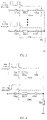
- FIG. 2 is a simplified analysis diagram of a single detection electrode and a display.
- a plurality of detection electrodes are distributed on a sensor 210 on the touch control screen.
- a single horizontal detection electrode TX1 is taken as an example for description.
- Capacitances C1 to Cn exist between a horizontal detection electrode TX1 211 and a display cathode plate 220, and a resistor R exists between the display cathode plate 220 and ground.
- the touch control screen sends an uplink spreading signal to the active pen through the horizontal detection electrode TX1 211, a large amount of energy passes through the capacitances C1-Cn and is coupled to the display cathode plate 220.
- uplink spreading signals VI to Vn may remain on the display cathode plate 220. These remaining uplink spreading signals V1 to Vn affect display data (DDIC Data) output by a display driving circuit 231 through capacitances Cdl to Cdn, thereby affecting display of a light-emitting diode D1 and finally causing visible moire on the display 230.
- DDIC Data display data
- FIG. 3 is a simplified analysis diagram of a plurality of detection electrodes and the display.
- An equivalent resistance Rs between the display cathode plate and ground is much smaller than an equivalent impedance of a detection electrode.
- ZTX1 to ZTXn are equivalent impedances of single detection electrodes, and RTX1 to RTXn are respective equivalent resistance of respective single detection electrode.
- the touch control screen transmits the uplink spreading signals to the active pen by simultaneously applying non-inverting drive signals to horizontal detection electrodes and/or longitudinal detection electrodes.
- the non-inverting drive signals needs to be applied to the plurality of detection electrodes simultaneously.
- the non-inverting drive signals are applied to all the horizontal detection electrodes or longitudinal detection electrodes, so that the uplink spreading signal received by the active pen is strong enough.
- the remaining uplink spreading signal Vn satisfies Vn ⁇ n * VTX, where n is a number of detection electrodes to which drive signals are applied, and VTX is a magnitude of the uplink spreading signal. That is, the greater the number of detection electrodes to which the drive signals are simultaneously applied, the larger the remaining uplink spreading signal Vn is in magnitude, and the easier for the moire to appear.
- the touch control screen When the active pen draws lines on the touch control screen, the touch control screen needs to display in real time drawing tracks of the active pen.
- the detection electrodes on a full screen of the touch control screen need to operate simultaneously, and at this time, the moire is thus easier to appear on the display.
- the present disclosure provides a signal driving method, which may enable the active pen to receive the uplink spreading signal sent by the touch control screen within the certain distance between the active pen and the touch control screen while keeping the drawing tracks of the active pen displayed on the touch control screen unbroken, and avoid visible moire or weaken the Moire phenomenon.
- FIG. 4 is a schematic diagram of a signal driving method according to an embodiment of the present disclosure.
- the touch control screen sends a correct uplink spreading signal to some detection electrodes, and the correct uplink spreading signal is referred to as a non-inverting drive signal.
- the touch control screen sends an uplink spreading signal with a phase opposite to that of the non-inverting drive signal to some other detection electrodes, and the uplink spreading signal is referred to as an inverting drive signal.
- the above uplink spreading signals are collectively referred to as drive signals. Using the inverting drive signal to cancel out the non-inverting drive signal, so as to minimize the magnitude of the remaining uplink spreading signal Vn, thereby resolving the effect of the moire.
- two adjacent detection electrodes are taken as an example for description.
- one of the two detection electrodes transmits the non-inverting drive signal to the active pen
- another detection electrode transmits the inverting drive signal to the active pen. If equivalent resistances of the two detection electrodes and self-capacitances of the two detection electrodes to ground are respectively equal, and the non-inverting drive signal and the inverting drive signal cancel each other out, there is no remaining uplink spreading signal, thereby avoiding interference caused by the uplink spreading signal to the display and resolving the effect of the moire. As shown in FIG. 5 , the more symmetrical the phases of the non-inverting and inverting drive signal, the better the cancelling is.
- the active pen and the touch control screen are two independent systems, which need to communicate and interact with each other based on an active pen protocol, so as to be used in coordination.
- an active pen protocol for example, a Microsoft pen protocol (MPP), a universal stylus initiative (USI) protocol, a Huawei pen protocol (HPP) and the like
- the touch control screen is required to send an uplink spreading signal to wake up and synchronize with the active pen.
- MPP Microsoft pen protocol
- USB universal stylus initiative
- HPP Huawei pen protocol
- HPP is taken as an example for description.
- a chip sequence prescribed in the active pen protocol is designated as the non-inverting drive signal, and a signal with a phase 180 degrees opposite to that of the non-inverting drive signal is designated as the inverting drive signal.
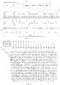
- an uplink spreading signal shown in FIG. 6 is defined as the non-inverting drive signal, and a phase of an uplink spreading signal shown in FIG. 7 differs 180 degrees from that of the uplink spreading signal shown in FIG. 7 , thus the uplink spreading signal shown in FIG. 7 is defined as the inverting drive signal.
- the uplink spreading signal shown in FIG. 6 " 1 " is denoted by a 31-bits code of 0x4259F1BA, "0" is denoted by a 31-bits code of 0x3DA60E45, and a duration of each bit is 1us.
- one signal driving cycle includes two signal driving periods in which drive signals are applied to P detection electrodes.
- the method includes: in a first signal driving period, applying non-inverting drive signals to M adjacent detection electrodes and applying inverting drive signals to N adjacent detection electrodes, where the non-inverting drive signals applied to the M adjacent detection electrodes and the inverting drive signals applied to the N adjacent detection electrodes cancel each other out, M+N ⁇ P and
- Q denotes a number of detection electrodes after the cancelling which makes an active pen not cause moire
- P denotes a number of detection electrodes not greater
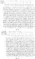
- the drive signals are applied to all horizontal detection electrodes TX1 to TX17 on the touch control screen.
- the non-inverting drive signals are applied to adjacent detection electrodes TX1 to TX9, and the inverting drive signals are applied to adjacent detection electrodes TX10 to TX17.
- the non-inverting drive signals applied to the 9 detection electrodes and the inverting drive signals applied to the 8 detection electrodes cancel each other out, and 1 detection electrode to which the non-inverting drive signal is applied is left. Moire caused by the positive pen is relevant to a number of detection electrodes left after the cancelling.
- the inverting drive signals are applied to adjacent detection electrodes TX1 to TX8, and the non-inverting drive signals are applied to adjacent detection electrodes TX9 to TX17.
- the non-inverting drive signals applied to the 9 detection electrodes and the inverting drive signals applied to the 8 detection electrodes cancel each other out, and 1 detection electrode to which the non-inverting drive signal is applied is left.
- a magnitude of the uplink spreading signal is small, which may not cause visible Moire phenomenon.
- the active pen is able to receive the non-inverting drive signals within a certain height range between the active pen and the touch control screen because the non-inverting drive signals are simultaneously applied to a plurality of detection electrodes at the position 1 in the first signal driving period. If the active pen is at position 2, the active pen is able to receive the non-inverting drive signals within a certain height range between the active pen and the touch control screen because the non-inverting drive signals are simultaneously applied to a plurality of detection electrodes at the position 2 in the second signal driving period.
- the active pen is at position 3
- strength of the non-inverting drive signal received by the active pen may be reduced because the inverting drive signals are applied to the detection electrodes TX10 and TX8 that are adjacent to the detection electrode TX9 in the first and second signal driving periods, so that the active pen is unable to receive the non-inverting drive signal from the touch control screen within a certain height range.
- a height at which the active pen is able to receive the non-inverting drive signal at the position 3 is lower than a height at which the active pen is able to receive the non-inverting drive signal at the position 1 or the position 2.
- the non-inverting drive signal is applied to TX9 in both the first signal driving period and the second signal driving period.
- the number of detection electrodes to which the non-inverting drive signals are applied in the two signal driving periods is 1.
- the non-inverting drive signals may be applied to a plurality of detection electrodes in both the first signal driving period and the second signal driving period. Since the non-inverting drive signals are applied to all the horizontal detection electrodes on the touch control screen in the first and second signal driving periods together, thus ensuring that the active pen is able to receive the non-inverting drive signals at any position on the touch control screen. In this way, the Moire phenomenon is avoided while ensuring the drawing tracks of the active pen unbroken.
- the drive signals are applied to 16 horizontal detection electrodes on the touch control screen.
- the non-inverting drive signals are applied to adjacent detection electrodes TX2 to TX9, and the inverting drive signals are applied to adjacent detection electrodes TX10 to TX17.
- the non-inverting drive signals applied to the 8 detection electrodes and the inverting drive signals applied to the 8 detection electrodes cancel each other out, and 0 detection electrode to which the drive signal is applied is left. There is no uplink spreading signal remaining on the cathode plate, thus achieving perfect cancelling.
- the inverting drive signals are applied to adjacent detection electrodes TX1 to TX8, and the non-inverting drive signals are applied to adjacent detection electrodes TX9 to TX16.
- the non-inverting drive signals applied to the 8 detection electrodes and the inverting drive signals applied to the 8 detection electrodes cancel each other out, and 0 detection electrode to which the drive signal is applied is left. There is no uplink spreading signal remaining on the cathode plate, thus achieving perfect cancelling.
- the non-inverting drive signal is applied to TX9 in both the first signal driving period and the second signal driving period.
- the non-inverting drive signals may be applied to the plurality of detection electrodes both the first signal driving period and the second signal driving period. That is, the number of detection electrodes to which the non-inverting drive signals are applied in the two signal driving periods is greater than or equal to 1, which is advantageous for keeping the drawing tracks of the active pen unbroken.
- the drive signals may be only applied to some of the horizontal detection electrodes.
- the touch control screen only applies the drive signals to detection electrodes TX2 to TX17 and do not apply the drive signals to the horizontal detection electrode TX1 disposed at the edge.
- the active pen rarely touches regions at the edge, so that use of the active pen may not be affected.
- the drive signals may be applied to the longitudinal detection electrodes on the full screen.
- the drive signals may be only applied to some of the longitudinal detection electrodes.
- no drive signal is applied to I detection electrodes in the first signal driving period, and no drive signal is applied to O detection electrodes in the second signal driving period.
- the I detection electrodes are located between the M adjacent detection electrodes and the N adjacent detection electrodes, and the O detection electrodes are located between the K adjacent detection electrodes and the L adjacent detection electrodes.
- the drive signals are applied to 17 horizontal detection electrodes on the touch control screen.
- the non-inverting drive signals are applied to adjacent detection electrodes TX1 to TX9
- the inverting drive signals are applied to adjacent detection electrodes TX11 to TX17
- no drive signal is applied to the detection electrode TX10 between the detection electrode TX9 to which the non-inverting drive signal is applied and the detection electrode TX11 to which the inverting drive signal is applied.
- the non-inverting drive signals applied to the 9 detection electrodes and the inverting drive signals applied to the 7 detection electrodes cancel each other out, and 2 detection electrodes to which the non-inverting drive signals are applied are left.
- Moire caused by the positive pen is relevant to a number of detection electrodes left after the cancelling.
- the inverting drive signals are applied to adjacent detection electrodes TX1 to TX7, the non-inverting drive signals are applied to adjacent detection electrodes TX9 to TX17, and no drive signal is applied to the detection electrode TX8 between the detection electrode TX9 to which the non-inverting drive signal is applied and the detection electrode TX7 to which the inverting drive signal is applied.
- Moire caused by the positive pen is relevant to a number of detection electrodes left after the cancelling.
- one signal driving cycle includes three signal driving periods in which drive signals are applied to P detection electrodes.
- ⁇ Q; in a second signal driving period, applying the non-inverting drive signals to K adjacent detection electrodes, applying the inverting drive signals to L adjacent detection electrodes, and not applying the drive signals to J detection electrodes, where the non-inverting drive signals applied to the K adjacent detection electrodes and the inverting drive signals applied to the L adjacent detection electrodes cancel each other out, K+L+J P and
- the drive signals are applied to horizontal detection electrodes TX1 to TX17 on the touch control screen.
- the non-inverting drive signals are applied to adjacent detection electrodes TX1 to TX6, the inverting drive signals are applied to adjacent detection electrodes TX7 to TX17, and no drive signal is applied to detection electrodes TX12 to TX17.
- the non-inverting drive signals applied to the 6 detection electrodes and the inverting drive signals applied to the 5 detection electrodes cancel each other out, and 1 detection electrode to which the non-inverting drive signal is applied is left. Moire caused by the positive pen is relevant to a number of detection electrodes left after the cancelling.
- no drive signal is applied to detection electrodes TX1 to TX5
- the non-inverting drive signals are applied to adjacent detection electrodes TX6 to TX11
- the inverting drive signals are applied to adjacent detection electrodes TX12 to TX17.
- the non-inverting drive signals applied to the 6 detection electrodes and the inverting drive signals applied to the 6 detection electrodes cancel each other out, and 0 detection electrode to which the drive signal is applied is left.
- no drive signal is applied to detection electrodes TX1 to TX5
- the inverting drive signals are applied to adjacent detection electrodes TX6 to TX10
- the non-inverting drive signals are applied to adjacent detection electrodes TX11 to TX17.
- the non-inverting drive signals applied to 7 detection electrodes and the inverting drive signals applied to the 5 detection electrodes cancel each other out, and 2 detection electrodes to which the non-inverting drive signals are applied are left.
- Q 2
- the non-inverting drive signals are applied to the detection electrodes TX6 and TX11 in two of the three signal driving periods.
- the non-inverting drive signals may be applied to the plurality of detection electrodes in two of the three signal driving periods. That is, the number of detection electrodes to which the non-inverting drive signals are applied in two of the three signal driving periods is greater than or equal to 2, which is advantageous for keeping the drawing tracks of the active pen unbroken.
- the number of detection electrodes left after the cancelling in the first signal driving period may be equal to the number of detection electrodes left after the cancelling in the second signal driving period
- the number of detection electrodes to which the non-inverting drive signals are applied is equal to the number of detection electrodes to which the inverting drive signals are applied in each period, so as to achieving the perfect cancelling, thus the visible Moire phenomenon may not appear.
- the drive signals may be only applied to some of horizontal detection electrodes. As shown in FIG. 14 , the touch control screen only applies the drive signals to detection electrodes TX2 to TX16, and do not apply the drive signals to the horizontal detection electrode TX1 and TX17 disposed at the edge. Generally, the active pen rarely touches regions at the edge, so that use of the active pen may not be affected.
- the drive signals may be applied to the longitudinal detection electrodes on the full screen.
- the drive signals may be only applied to some of the longitudinal detection electrodes.
- no drive signal is applied to I detection electrodes, and the I detection electrodes are located between the M adjacent detection electrodes and the N adjacent detection electrodes.
- no drive signal is applied to O detection electrodes, and the O detection electrodes are located between the K adjacent detection electrodes and the L adjacent detection electrodes.
- no drive signal is applied to P detection electrodes, and the P detection electrodes are located between the G adjacent detection electrodes and the H adjacent detection electrodes.
- the drive signals are applied to 17 horizontal detection electrodes on the touch control screen.
- the non-inverting drive signals are applied to adjacent detection electrodes TX1 to TX6, the inverting drive signals are applied to adjacent detection electrodes TX8 to TX13, and no drive signal is applied to the detection electrodes TX7 and TX14 to TX17.
- the detection electrode TX7 to which no drive signal is applied is located between the detection electrode TX6 to which the non-inverting drive signal is applied and the detection electrode TX8 to which the inverting drive signal is applied.
- the non-inverting drive signals applied to the 6 detection electrodes and the inverting drive signals applied to the 6 detection electrodes cancel each other out, and 0 detection electrode to which the drive signal is applied is left.
- the inverting drive signals are applied to adjacent detection electrodes TX1 to TX4 and TX13 to TX14, the non-inverting drive signals are applied to adjacent detection electrodes TX6 to TX11, and no drive signal is applied to the detection electrodes TX5, TX12 and TX15 to TX17.
- the detection electrode TX5 to which no drive signal is applied is located between the detection electrode TX6 to which the non-inverting drive signal is applied and the detection electrode TX4 to which the inverting drive signal is applied.
- the detection electrode TX12 to which no drive signal is applied is located between the detection electrode TX11 to which the non-inverting drive signal is applied and the detection electrode TX13 to which the inverting drive signal is applied.
- the non-inverting drive signals applied to the 6 detection electrodes and the inverting drive signals applied to the 6 detection electrodes cancel each other out, and 0 detection electrode to which the drive signal is applied is left.
- adjacent detection electrodes TX3 to TX9 to which the inverting drive signal is applied, the non-inverting drive signals are applied to adjacent detection electrodes TX11 to TX17, and no drive signal is applied to the detection electrodes TX1 to TX2 and TX10.
- the detection electrode TX10 to which no drive signal is applied is located between the detection electrode TX11 to which the non-inverting drive signal is applied and the detection electrode TX9 to which the inverting drive signal is applied.
- the non-inverting drive signals applied to the 6 detection electrodes and the inverting drive signals applied to the 6 detection electrodes cancel each other out, and 0 detection electrode to which the drive signal is applied is left.
- one signal driving cycle includes four signal driving periods in which drive signals are applied to P detection electrodes.
- ⁇ Q; in a second signal driving period, applying the non-inverting drive signals to K adjacent detection electrodes, applying the inverting drive signals to L adjacent detection electrodes, and not applying the drive signals to J detection electrodes, where the non-inverting drive signals applied to the K adjacent detection electrodes and the inverting drive signals applied to the L adjacent detection electrodes cancel each other out, K+L+J P and
- the drive signals are applied to horizontal detection electrodes TX1 to TX17 on the touch control screen.
- the non-inverting drive signals are applied to adjacent detection electrodes TX1 to TX5
- the inverting drive signals are applied to adjacent detection electrodes TX6 to TX10
- no drive signal is applied to the detection electrodes TX11 to TX17.
- the non-inverting drive signals applied to the 5 detection electrodes and the inverting drive signals applied to the 5 detection electrodes cancel each other out, and 0 detection electrode to which the drive signal is applied is left. Moire caused by the positive pen is relevant to a number of detection electrodes left after the cancelling.
- no drive signal is applied to the detection electrodes TX1 to TX4 and TX14 to TX17, the non-inverting drive signals are applied to adjacent detection electrodes TX5 to TX9, and the inverting drive signals are applied to adjacent detection electrodes TX10 to TX13.
- the non-inverting drive signals applied to the 5 detection electrodes and the inverting drive signals applied to the 4 detection electrodes cancel each other out, and 1 detection electrode to which the non-inverting drive signal is applied is left.
- no drive signal is applied to the detection electrodes TX1 to TX4 and TX14 to TX17
- the inverting drive signals are applied to adjacent detection electrodes TX5 to TX8
- the non-inverting drive signals are applied to adjacent detection electrodes TX9 to TX13.
- the non-inverting drive signals applied to the 5 detection electrodes and the inverting drive signals applied to the 4 detection electrodes cancel each other out, and 1 detection electrode to which the non-inverting drive signal is applied is left.
- no drive signal is applied to the detection electrodes TX1 to TX8
- the inverting drive signals are applied to adjacent detection electrodes TX9 to TX12
- the non-inverting drive signals are applied to adjacent detection electrodes TX13 to TX17.
- the non-inverting drive signals applied to the 5 detection electrodes and the inverting drive signals applied to the 4 detection electrodes cancel each other out, and 1 detection electrode to which the non-inverting drive signal is applied is left.
- the non-inverting drive signals are applied to the detection electrodes TX5, TX9 and TX13 in two of the four signal driving periods.
- the non-inverting drive signals may be applied to the plurality of detection electrodes in two of the four signal driving periods. That is, the number of detection electrodes to which the non-inverting drive signals are applied in two of the four signal driving periods is greater than or equal to 3, which is advantageous for keeping the drawing tracks of the active pen unbroken.
- the number of detection electrodes left after the cancelling in the first signal driving period may be equal to the number of detection electrodes left after the cancelling in the second signal driving period
- the number of detection electrodes left after the cancelling in the second signal driving period may be equal to the number of detection electrodes left after the cancelling in the third signal driving period
- the drive signals may be only applied to some of the horizontal detection electrodes. As shown in FIG. 17 , the touch control screen only applies the drive signals to detection electrodes TX2 to TX16, and do not apply the drive signals to the horizontal detection electrodes TX1 and TX17 disposed at the edge. Generally, the active pen rarely touches regions at the edge, so that use of the active pen may not be affected.
- the drive signals may be applied to the longitudinal detection electrodes on the full screen.
- the drive signals may be only applied to some of the longitudinal detection electrodes.
- no drive signal is applied to I detection electrodes, and the I detection electrodes are located between the M adjacent detection electrodes and the N adjacent detection electrodes.
- no drive signal is applied to O detection electrodes, and the O detection electrodes are located between the K adjacent detection electrodes and the L adjacent detection electrodes.
- no drive signal is applied to P detection electrodes, and the P detection electrodes are located between the G adjacent detection electrodes and the H adjacent detection electrodes.
- no drive signal is applied to W detection electrodes, and the W detection electrodes are located between the T adjacent detection electrodes and the Y adjacent detection electrodes.
- the drive signals are applied to 17 horizontal detection electrodes on the touch control screen.
- the non-inverting drive signals are applied to adjacent detection electrodes TX1 to TX5
- the inverting drive signals are applied to adjacent detection electrodes TX7 to TX11
- no drive signal is applied to the detection electrodes TX6 and TX12 to TX17.
- the detection electrode TX6 to which no drive signal is applied is located between the detection electrode TX5 to which the non-inverting drive signal is applied and the detection electrode TX7 to which the inverting drive signal is applied.
- no drive signal is applied to the detection electrodes TX1 to TX4, TX10 and TX11 to TX15, the non-inverting drive signals are applied to adjacent detection electrodes TX5 to TX9, and the inverting drive signals are applied to adjacent detection electrodes TX15 to TX17.
- the detection electrode TX10 to which no drive signal is applied is located between the detection electrode TX9 to which the non-inverting drive signal is applied and the detection electrode TX11 to which the inverting drive signal is applied.
- the inverting drive signals are applied to adjacent detection electrodes TX3 to TX7, the non-inverting drive signals are applied to adjacent detection electrodes TX9 to TX13, and no drive signal is applied to the detection electrodes TX1 to TX2, TX8 and TX14 to TX17.
- the detection electrode TX8 to which no drive signal is applied is located between the detection electrode TX9 to which the non-inverting drive signal is applied and the detection electrode TX7 to which the inverting drive signal is applied.
- the inverting drive signals are applied to adjacent detection electrodes TX7 to TX11, the non-inverting drive signals are applied to adjacent detection electrodes TX13 to TX17, and no drive signal is applied to the detection electrodes TX1 to TX6 and TX12.
- the detection electrode TX12 to which no drive signal is applied is located between the detection electrode TX13 to which the non-inverting drive signal is applied and the detection electrode TX11 to which the inverting drive signal is applied.
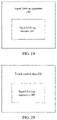
- a signal driving apparatus 200 includes: a signal driving module, configured to: in a first signal driving period, apply non-inverting drive signals to M adjacent detection electrodes and apply inverting drive signals to N adjacent detection electrodes, where the non-inverting drive signals applied to the M adjacent detection electrodes and the inverting drive signals applied to the N adjacent detection electrodes cancel each other out, M+N ⁇ P and
- the detection electrodes are horizontal detection electrodes or longitudinal detection electrodes
- P denotes a number of the horizontal detection electrodes or a number of the longitudinal detection electrodes.
- a number of detection electrodes to which the non-inverting drive signals are applied in the two signal driving periods is greater than or equal to 1.
- the coding module is further configured to: in the first signal driving period, not apply the drive signals to I detection electrodes; in the second signal driving period, not apply the drive signals to O detection electrodes; where the I detection electrodes are located between the M adjacent detection electrodes and the N adjacent detection electrodes, and the O detection electrodes are located between the K adjacent detection electrodes and the L adjacent detection electrodes.
- M-N K-L.
- the detection electrodes are horizontal detection electrodes or longitudinal detection electrodes
- P denotes a number of the horizontal detection electrodes or a number of the longitudinal detection electrodes.
- a number of detection electrodes to which the non-inverting drive signals are applied in two of the three signal driving periods is greater than or equal to 2.
- the signal driving module is further configured to: in the first signal driving period, not apply the drive signals to I detection electrodes, wherein the I detection electrodes are located between the M adjacent detection electrodes and the N adjacent detection electrodes; in the second signal driving period, not apply the drive signals to O detection electrodes, wherein the O detection electrodes are located between the K adjacent detection electrodes and the L adjacent detection electrodes; and in the third signal driving period, not apply the drive signals to P detection electrodes, wherein the P detection electrodes are located between the G adjacent detection electrodes and the H adjacent detection electrodes; wherein I ⁇ B, O ⁇ J and P ⁇ F.
- the detection electrodes are horizontal detection electrodes or longitudinal detection electrodes
- P denotes a number of the horizontal detection electrodes or a number of the longitudinal detection electrodes.
- a number of detection electrodes to which the non-inverting drive signals are applied in two of the four signal driving periods is greater than or equal to 3.
- the signal driving module is further configured to: in the first signal driving period, not apply the drive signals to I detection electrodes, wherein the I detection electrodes are located between the M adjacent detection electrodes and the N adjacent detection electrodes; in the second signal driving period, not apply the drive signals to O detection electrodes, wherein the O detection electrodes are located between the K adjacent detection electrodes and the L adjacent detection electrodes; in the third signal driving period, not apply the drive signals to P detection electrodes, wherein the P detection electrodes are located between the G adjacent detection electrodes and the H adjacent detection electrodes; and in the fourth signal driving period, not apply the drive signals to W detection electrodes, wherein the W detection electrodes are located between the T adjacent detection electrodes and the Y adjacent detection electrodes; wherein I ⁇ B, O ⁇ J, P ⁇ F and W ⁇ U.
- a touch control chip 203 may include the signal driving apparatus 200 shown in FIG. 19 .
Landscapes
- Engineering & Computer Science (AREA)
- General Engineering & Computer Science (AREA)
- Theoretical Computer Science (AREA)
- Human Computer Interaction (AREA)
- Physics & Mathematics (AREA)
- General Physics & Mathematics (AREA)
- Position Input By Displaying (AREA)
- Electronic Switches (AREA)
Abstract
Description
- The present disclosure relates to the field of information technology, in particular to a signal driving method, a signal driving apparatus and a touch control chip.
- Currently, as a main peripheral input accessory of an electronic device, an active pen gradually receives attention from the market. A certain number of detection electrodes are distributed on a touch control screen in the horizontal direction and vertical direction. Therefore, an uplink spreading signal may be sent by the detection electrode to the active pen. After synchronization with the active pen is established, a downlink signal is sent from a tip of the active pen through the detection electrode, and two-dimensional position coordinates of the tip of the active pen on the touch control screen is calculated according to the downlink signal.
- The inventor found that various forms of display ripples appear on the display when using the active pen to operate the electronic device, which sometimes move forward like water ripples, sometimes present few moving bright lines, or sometimes appear at times. These phenomena are collectively referred to as Moire phenomenon. Therefore, it is urgent that how to effectively solve Moire phenomenon on the display.
- The present disclosure provides a signal driving method, a signal driving apparatus and a touch control chip, which may effectively solve Moire phenomenon appearing on a display.
- In one aspect, the present disclosure provides a signal driving method, wherein one signal driving cycle includes two signal driving periods in which drive signals are applied to P detection electrodes, and the method includes: in a first signal driving period, applying non-inverting drive signals to M adjacent detection electrodes and applying inverting drive signals to N adjacent detection electrodes, wherein the non-inverting drive signals applied to the M adjacent detection electrodes and the inverting drive signals applied to the N adjacent detection electrodes cancel each other out, M+N≤P and |M-N|≤Q; and in a second signal driving period, applying the non-inverting drive signals to K adjacent detection electrodes and applying the inverting drive signals to L adjacent detection electrodes, wherein the non-inverting drive signals applied to the K adjacent detection electrodes and the inverting drive signals applied to the L adjacent detection electrodes cancel each other out, K+L≤P, |K-L|≤Q and M+K≥P; wherein Q denotes a number of detection electrodes which makes an active pen not cause moire after the cancelling, and P denotes a number of detection electrodes not greater than a number of detection electrodes on a touch control screen.
- According to the first aspect, in a possible implementation, the detection electrodes are horizontal detection electrodes or longitudinal detection electrodes, and P denotes a number of the horizontal detection electrodes or a number of the longitudinal detection electrodes.
- According to the first aspect, in a possible implementation, a number of detection electrodes to which the non-inverting drive signals are applied in the two signal driving periods is greater than or equal to 1.
- According to the first aspect, in a possible implementation, code, the method further includes: in the first signal driving period, not applying the drive signals to I detection electrodes; in the second signal driving period, not applying the drive signals to O detection electrodes; wherein the I detection electrodes are located between the M adjacent detection electrodes and the N adjacent detection electrodes, and the O detection electrodes are located between the K adjacent detection electrodes and the L adjacent detection electrodes.
- According to the first aspect, in a possible implementation, 1=1 and O=1.
- According to the first aspect, in a possible implementation, Q=2 or Q=1.
- According to the first aspect, in a possible implementation, M-N=K-L.
- In a second aspect, another signal driving method is provided, wherein one signal driving cycle includes three signal driving periods in which drive signals are applied to P detection electrodes, and the method includes: in a first signal driving period, applying non-inverting drive signals to M adjacent detection electrodes, applying inverting drive signals to N adjacent detection electrodes, and not applying the drive signals to B detection electrodes, wherein the non-inverting drive signals applied to the M adjacent detection electrodes and the inverting drive signals applied to the N adjacent detection electrodes cancel each other out, M+N+B=P and |M-N|≤Q; in a second signal driving period, applying the non-inverting drive signals to K adjacent detection electrodes, applying the inverting drive signals to L adjacent detection electrodes, and not applying the drive signals to J detection electrodes, wherein the non-inverting drive signals applied to the K adjacent detection electrodes and the inverting drive signals applied to the L adjacent detection electrodes cancel each other out, K+L+J=P and |K-L|≤Q; and in a third signal driving period, applying the non-inverting drive signals to G adjacent detection electrodes, applying the inverting drive signals to H adjacent detection electrodes, and not applying the drive signals to F detection electrodes, wherein the non-inverting drive signals applied to the G adjacent detection electrodes and the inverting drive signals applied to the H adjacent detection electrodes cancel each other out, G+H+F=P, |G-H|≤Q and M+K+H≥P; wherein Q denotes a number of detection electrodes after the cancelling which makes an active pen not cause moire, and P denotes a number of detection electrodes not greater than a number of detection electrodes on a touch control screen.
- According to the second aspect, in a possible implementation, the detection electrodes are horizontal detection electrodes or longitudinal detection electrodes, and P denotes a number of the horizontal detection electrodes or a number of the longitudinal detection electrodes.
- According to the second aspect, in a possible implementation, a number of detection electrodes to which the non-inverting drive signals are applied in two of the three signal driving periods is greater than or equal to 2.
- According to the second aspect, in a possible implementation, the method further includes: in the first signal driving period, not applying the drive signals to I detection electrodes, wherein the I detection electrodes are located between the M adjacent detection electrodes and the N adjacent detection electrodes; in the second signal driving period, not applying the drive signals to O detection electrodes, wherein the O detection electrodes are located between the K adjacent detection electrodes and the L adjacent detection electrodes; and in the third signal driving period, not applying the drive signals to P detection electrodes, wherein the P detection electrodes are located between the G adjacent detection electrodes and the H adjacent detection electrodes; wherein I<B, O<J and P<F.
- According to the second aspect, in a possible implementation, I=1, O=1 and P=1.
- According to the second aspect, in a possible implementation, Q=2 or Q=1.
- According to the second aspect, in a possible implementation, M-N= K-L=G-H.
- In a third aspect, another signal driving method is provided, wherein one signal driving cycle includes four signal driving periods in which drive signals are applied to P detection electrodes, and the method includes: in a first signal driving period, applying non-inverting drive signals to M adjacent detection electrodes, applying inverting drive signals to N adjacent detection electrodes, and not applying the drive signals to B detection electrodes, wherein the non-inverting drive signals applied to the M adjacent detection electrodes and the inverting drive signals applied to the N adjacent detection electrodes cancel each other out, M+N+B=P and | M-N | ≤Q; in a second signal driving period, applying the non-inverting drive signals to K adjacent detection electrodes, applying the inverting drive signals to L adjacent detection electrodes, and not applying the drive signals to J detection electrodes, wherein the non-inverting drive signals applied to the K adjacent detection electrodes and the inverting drive signals applied to the L adjacent detection electrodes cancel each other out, K+L+J=P and | K-L | ≤Q; in a third signal driving period, applying the non-inverting drive signals to G adjacent detection electrodes, applying the inverting drive signals to H adjacent detection electrodes, and not applying the drive signals to F detection electrodes, wherein the non-inverting drive signals applied to the K adjacent detection electrodes and the inverting drive signals applied to the L adjacent detection electrodes cancel each other out, G+H+F=P and | G-H | ≤Q; and in a fourth signal driving period, applying the non-inverting drive signals to T adjacent detection electrodes, applying the inverting drive signals to Y adjacent detection electrodes, and not applying the drive signals to U detection electrodes, wherein the non-inverting drive signals applied to the T adjacent detection electrodes and the inverting drive signals applied to the Y adjacent detection electrodes cancel each other out, T+Y+U=P, | T-Y | ≤Q and M+K+H+T≥P; wherein Q denotes a number of detection electrodes after the cancelling which makes an active pen not cause moire, and P denotes a number of detection electrodes not greater than a number of detection electrodes on a touch control screen.
- According to the third aspect, in a possible implementation, the detection electrodes are horizontal detection electrodes or longitudinal detection electrodes, and P denotes a number of the horizontal detection electrodes or a number of the longitudinal detection electrodes.
- According to the third aspect, in a possible implementation, a number of detection electrodes to which the non-inverting drive signals are applied in two of the four signal driving periods is greater than or equal to 3.
- According to the third aspect, in the first signal driving period, the method further includes: in the first signal driving period, not applying the drive signals to I detection electrodes, wherein the I detection electrodes are located between the M adjacent detection electrodes and the N adjacent detection electrodes; in the second signal driving period, not applying the drive signals to O detection electrodes, wherein the O detection electrodes are located between the K adjacent detection electrodes and the L adjacent detection electrodes; in the third signal driving period, not applying the drive signals to P detection electrodes, wherein the P detection electrodes are located between the G adjacent detection electrodes and the H adjacent detection electrodes; and in the fourth signal driving period, not applying the drive signals to W detection electrodes, wherein the W detection electrodes are located between the T adjacent detection electrodes and the Y adjacent detection electrodes; wherein I<B, O<J, P<F and W<U.
- According to the third aspect, in a possible implementation, 1=1, O=1, P=1 and W=1.
- According to the third aspect, in a possible implementation, M-N= K-L=G-H=T-Y.
- In a fourth aspect, a signal driving apparatus is provided, wherein one signal driving cycle includes two signal driving periods in which drive signals are applied to P detection electrodes, and the apparatus includes: a signal driving module, configured to: in a first signal driving period, apply non-inverting drive signals to M adjacent detection electrodes and apply inverting drive signals to N adjacent detection electrodes, wherein the non-inverting drive signals applied to the M adjacent detection electrodes and the inverting drive signals applied to the N adjacent detection electrodes cancel each other out, M+N≤P and | M-N | ≤Q; and in a second signal driving period, apply the non-inverting drive signals to K adjacent detection electrodes and apply the inverting drive signals to L adjacent detection electrodes, wherein the non-inverting drive signals applied to the K adjacent detection electrodes and the inverting drive signals applied to the L adjacent detection electrodes cancel each other out, K+L≤P, | K-L | ≤Q and M+K≥P; wherein Q denotes a number of detection electrodes after the cancelling which makes an active pen not cause moire, and P denotes a number of detection electrodes not greater than a number of detection electrodes on a touch control screen.
- According to the fourth aspect, in a possible implementation, the detection electrodes are horizontal detection electrodes or longitudinal detection electrodes, and P denotes a number of the horizontal detection electrodes or a number of the longitudinal detection electrodes.
- According to the fourth aspect, in a possible implementation, a number of detection electrodes to which the non-inverting drive signals are applied in the two signal driving periods is greater than or equal to 1.
- According to the fourth aspect, in a possible implementation, the signal driving module is further configured to: in the first signal driving period, not apply the drive signals to I detection electrodes; in the second signal driving period, not apply the drive signals to O detection electrodes; wherein the I detection electrodes are located between the M adjacent detection electrodes and the N adjacent detection electrodes, and the O detection electrodes are located between the K adjacent detection electrodes and the L adjacent detection electrodes.
- According to the fourth aspect, in a possible implementation, 1=1 and O=1.
- According to the fourth aspect, in a possible implementation, Q=2 or Q=1.
- According to the fourth aspect, in a possible implementation, M-N=K-L.
- In a fifth aspect, a signal driving apparatus is provided, wherein one signal driving cycle includes three signal driving periods in which drive signals are applied to P detection electrodes, and the apparatus includes: a signal driving module, configured to: in a first signal driving period, apply non-inverting drive signals to M adjacent detection electrodes, apply inverting drive signals to N adjacent detection electrodes, and not apply the drive signals to B detection electrodes, wherein the non-inverting drive signals applied to the M adjacent detection electrodes and the inverting drive signals applied to the N adjacent detection electrodes cancel each other out, M+N+B=P and | M-N | ≤Q; in a second signal driving period, apply the non-inverting drive signals to K adjacent detection electrodes, apply the inverting drive signals to L adjacent detection electrodes, and not apply the drive signals to J detection electrodes, wherein the non-inverting drive signals applied to the K adjacent detection electrodes and the inverting drive signals applied to the L adjacent detection electrodes cancel each other out, K+L+J=P and | K-L | ≤Q; and in a third signal driving period, apply the non-inverting drive signals to G adjacent detection electrodes, apply the inverting drive signals to H adjacent detection electrodes, and not apply the drive signals to F detection electrodes, wherein the non-inverting drive signals applied to the G adjacent detection electrodes and the inverting drive signals applied to the H adjacent detection electrodes cancel each other out, G+H+F=P, I G-H | ≤Q and M+K+H≥P; wherein Q denotes a number of detection electrodes after the cancelling which makes an active pen not cause moire, and P denotes a number of detection electrodes not greater than a number of detection electrodes on a touch control screen.
- According to the fifth aspect, in a possible implementation, the detection electrodes are horizontal detection electrodes or longitudinal detection electrodes, and P denotes a number of the horizontal detection electrodes or a number of the longitudinal detection electrodes.
- According to the fifth aspect, in a possible implementation, a number of detection electrodes to which the non-inverting drive signals are applied in two of the three signal driving periods is greater than or equal to 2.
- According to the fifth aspect, in a possible implementation, the signal driving module is further configured to: in the first signal driving period, not apply the drive signals to I detection electrodes, wherein the I detection electrodes are located between the M adjacent detection electrodes and the N adjacent detection electrodes; in the second signal driving period, not apply the drive signals to O detection electrodes, wherein the O detection electrodes are located between the K adjacent detection electrodes and the L adjacent detection electrodes; and in the third signal driving period, not apply the drive signals to P detection electrodes, wherein the P detection electrodes are located between the G adjacent detection electrodes and the H adjacent detection electrodes; wherein I<B, O<J and P<F.
- According to the fifth aspect, in a possible implementation, I=1, 0=1 and P=1.
- According to the fifth aspect, in a possible implementation, Q=2 or Q=1.
- According to the fifth aspect, in a possible implementation, M-N= K-L=G-H.
- In a sixth aspect, another signal driving apparatus is provided, wherein one signal driving cycle includes four signal driving periods in which drive signals are applied to P detection electrodes, and the apparatus includes: a signal driving module, configured to: in a first signal driving period, apply non-inverting drive signals to M adjacent detection electrodes, apply inverting drive signals to N adjacent detection electrodes, and not apply the drive signals to B detection electrodes, wherein the non-inverting drive signals applied to the M adjacent detection electrodes and the inverting drive signals applied to the N adjacent detection electrodes cancel each other out, M+N+B=P and | M-N | ≤Q; in a second signal driving period, apply the non-inverting drive signals to K adjacent detection electrodes, apply the inverting drive signals to L adjacent detection electrodes, and not apply the drive signals to J detection electrodes, wherein the non-inverting drive signals applied to the K adjacent detection electrodes and the inverting drive signals applied to the L adjacent detection electrodes cancel each other out, K+L+J=P and | K-L | ≤Q; in a third signal driving period, apply the non-inverting drive signals to G adjacent detection electrodes, apply the inverting drive signals to H adjacent detection electrodes, and not apply the drive signals to F detection electrodes, wherein the non-inverting drive signals applied to the K adjacent detection electrodes and the inverting drive signals applied to the L adjacent detection electrodes cancel each other out, G+H+F=P and | G-H | ≤Q; and in a fourth signal driving period, apply the non-inverting drive signals to T adjacent detection electrodes, apply the inverting drive signals to Y adjacent detection electrodes, and not apply the drive signals to U detection electrodes, wherein the non-inverting drive signals applied to the T adjacent detection electrodes and the inverting drive signals applied to the Y adjacent detection electrodes cancel each other out, T+Y+U=P, | T-Y | ≤Q and M+K+H+T≥P; wherein Q denotes a number of detection electrodes after the cancelling which makes an active pen not cause moire, and P denotes a number of detection electrodes not greater than a number of detection electrodes on a touch control screen.
- According to the sixth aspect, in a possible implementation, the detection electrodes are horizontal detection electrodes or longitudinal detection electrodes, and P denotes a number of the horizontal detection electrodes or a number of the longitudinal detection electrodes.
- According to the sixth aspect, in a possible implementation, a number of detection electrodes to which the non-inverting drive signals are applied in two of the four signal driving periods is greater than or equal to 3.
- According to the sixth aspect, in a possible implementation, the signal driving module is further configured to: in the first signal driving period, not apply the drive signals to I detection electrodes, wherein the I detection electrodes are located between the M adjacent detection electrodes and the N adjacent detection electrodes; in the second signal driving period, not apply the drive signals to O detection electrodes, wherein the O detection electrodes are located between the K adjacent detection electrodes and the L adjacent detection electrodes; in the third signal driving period, not apply the drive signals to P detection electrodes, wherein the P detection electrodes are located between the G adjacent detection electrodes and the H adjacent detection electrodes; and in the fourth signal driving period, not apply the drive signals to W detection electrodes, wherein the W detection electrodes are located between the T adjacent detection electrodes and the Y adjacent detection electrodes; wherein I<B, O<J, P<F and W<U.
- According to the sixth aspect, in a possible implementation, 1=1, O=1, P=1 and W=1.
- According to the sixth aspect, in a possible implementation, M-N= K-L=G-H=T-Y.
- In a seventh aspect, a touch control chip is provided, which includes the signal driving apparatus according to any one of the above aspects.
- Based on the above technical solutions, one signal driving cycle includes a plurality of signal driving periods in which drive signals are applied to P detection electrodes. In each signal driving period, non-inverting drive signals are applied to a part of the detection electrodes while inverting drive signals are applied to the other part of the detection electrodes. A number of detection electrodes to which the non-inverting drive signals are applied after the cancelling is smaller than a number of detection electrodes which makes an active pen not cause moire. In the plurality of signal driving periods, the non-inverting drive signals are applied to all the P detection electrodes, thereby solving the Moire phenomenon on a display while keeping the drawing tracks of the active pen on the display unbroken.
- One or more embodiments are described as examples with reference to the corresponding figures in the accompanying drawings, and the examples do not constitute a limitation to the embodiments. The figures in the accompanying drawings do not constitute a proportion limitation unless otherwise stated. The division of the following embodiments is convenient for description, and should not constitute any limitation to specific implementation of the present disclosure. Each of the embodiments may be combined with or refer to each other without contradiction.
-
FIG. 1 is a schematic diagram illustrating the principle for use of an active pen on a touch control screen. -
FIG. 2 is a schematic diagram illustrating principle analysis for generation of moire when a single detection electrode is in operation. -
FIG. 3 is a schematic diagram illustrating principle analysis for generation of moire when a plurality of detection electrodes are in operation. -
FIG. 4 is a schematic diagram of a signal driving method according to an embodiment of the present disclosure. -
FIG. 5 is a schematic diagram of analysis on a non-inverting drive signal and an inverting drive signal according to an embodiment of the present disclosure. -
FIG. 6 is a schematic diagram of a timing of a non-inverting drive signal according to an embodiment of the present disclosure. -
FIG. 7 is a schematic diagram of a timing of an inverting drive signal according to an embodiment of the present disclosure. -
FIG. 8 is a schematic diagram of a possible implementation of a signal driving method according to an embodiment of the present disclosure. -
FIG. 9 is a schematic diagram of a possible implementation of a signal driving method according to another embodiment of the present disclosure. -
FIG. 10 is a schematic diagram of a possible implementation of a signal driving method according to another embodiment of the present disclosure. -
FIG. 11 is a schematic diagram of a possible implementation of a signal driving method according to another embodiment of the present disclosure. -
FIG. 12 is a schematic diagram of a possible implementation of a signal driving method according to another embodiment of the present disclosure. -
FIG. 13 is a schematic diagram of a possible implementation of a signal driving method according to another embodiment of the present disclosure. -
FIG. 14 is a schematic diagram of a possible implementation of a signal driving method according to another embodiment of the present disclosure. -
FIG. 15 is a schematic diagram of a possible implementation of a signal driving method according to another embodiment of the present disclosure. -
FIG. 16 is a schematic diagram of a possible implementation of a signal driving method according to another embodiment of the present disclosure. -
FIG. 17 is a schematic diagram of a possible implementation of a signal driving method according to another embodiment of the present disclosure. -
FIG. 18 is a schematic diagram of a possible implementation of a signal driving method according to still another embodiment of the present disclosure. -
FIG. 19 is a schematic block diagram of a signal driving apparatus according to an embodiment of the present disclosure. -
FIG. 20 is a schematic block diagram of a touch control chip according to an embodiment of the present disclosure. - In order to make the objectives, the technical solutions and the advantages of the present disclosure clearer, some embodiments of the present disclosure will be further described in the following with reference to the accompanying drawings. It shall be appreciated that the particular embodiments described herein are only meant to explain rather than limit the present disclosure.
- With reference to
FIG. 1 , a certain number of detection electrodes are distributed on atouch control screen 120. The detection electrodes include horizontal detection electrodes and longitudinal detection electrodes. Anactive pen 110 needs to receive anuplink spreading signal 131 sent from thetouch control screen 120 through the horizontal detection electrode and/or the longitudinal detection electrode. After receiving a correct uplink spreading signal, theactive pen 110 sends adownlink signal 132 to thetouch control screen 120. A Bluetooth chip 111 of theactive pen 110 receives information, for example, a frequency of the downlink signal, transmitted by aBluetooth chip 121 of thetouch control screen 120. Herein, theuplink spreading signal 131 sent from thetouch control screen 120 is configured to wake up theactive pen 110 and cause thetouch control screen 120 to establish synchronization with theactive pen 110. Thedownlink signal 132 sent by theactive pen 110 is configured to compute two-dimensional location coordinates of theactive pen 110 on thetouch control screen 120. - With reference to
FIG. 2, FIG. 2 is a simplified analysis diagram of a single detection electrode and a display. A plurality of detection electrodes are distributed on asensor 210 on the touch control screen. In this embodiment, a single horizontal detection electrode TX1 is taken as an example for description. Capacitances C1 to Cn exist between a horizontaldetection electrode TX1 211 and adisplay cathode plate 220, and a resistor R exists between thedisplay cathode plate 220 and ground. When the touch control screen sends an uplink spreading signal to the active pen through the horizontaldetection electrode TX1 211, a large amount of energy passes through the capacitances C1-Cn and is coupled to thedisplay cathode plate 220. Due to existence of the resistor R, some uplink spreading signals VI to Vn may remain on thedisplay cathode plate 220. These remaining uplink spreading signals V1 to Vn affect display data (DDIC Data) output by adisplay driving circuit 231 through capacitances Cdl to Cdn, thereby affecting display of a light-emitting diode D1 and finally causing visible moire on thedisplay 230. - In a conventional touch control screen, self-capacitances between horizontal detection electrodes and ground and self-capacitances between longitudinal detection electrodes and ground are both around 100Pf. In a Y-OCTA touch control screen, however, self-capacitances between horizontal detection electrodes and ground and self-capacitances between longitudinal detection electrodes and ground are both around 500Pf. Compared with the conventional touch control screen, the uplink spreading signal sent by the Y-OCTA touch control screen is easier to be coupled to the display. The larger the remaining uplink spreading signals are in magnitude, the more evident the moire is.
- With reference to
FIG. 3, FIG. 3 is a simplified analysis diagram of a plurality of detection electrodes and the display. An equivalent resistance Rs between the display cathode plate and ground is much smaller than an equivalent impedance of a detection electrode. ZTX1 to ZTXn are equivalent impedances of single detection electrodes, and RTX1 to RTXn are respective equivalent resistance of respective single detection electrode. In application of the active pen, the touch control screen transmits the uplink spreading signals to the active pen by simultaneously applying non-inverting drive signals to horizontal detection electrodes and/or longitudinal detection electrodes. In order to ensure that the active pen is able to receive the uplink spreading signals sent by the touch control screen within a certain distance between the active pen and the touch control screen, the non-inverting drive signals needs to be applied to the plurality of detection electrodes simultaneously. For example, the non-inverting drive signals are applied to all the horizontal detection electrodes or longitudinal detection electrodes, so that the uplink spreading signal received by the active pen is strong enough. However, the remaining uplink spreading signal Vn satisfies Vn ∝ n * VTX, where n is a number of detection electrodes to which drive signals are applied, and VTX is a magnitude of the uplink spreading signal. That is, the greater the number of detection electrodes to which the drive signals are simultaneously applied, the larger the remaining uplink spreading signal Vn is in magnitude, and the easier for the moire to appear. - When the active pen draws lines on the touch control screen, the touch control screen needs to display in real time drawing tracks of the active pen. In order to ensure the drawing tracks of the active pen displayed on the touch control screen unbroken and the active pen being able to receive the uplink spreading signal sent by the touch control screen within a certain distance between the active pen and the touch control screen, the detection electrodes on a full screen of the touch control screen need to operate simultaneously, and at this time, the moire is thus easier to appear on the display.
- Accordingly, the present disclosure provides a signal driving method, which may enable the active pen to receive the uplink spreading signal sent by the touch control screen within the certain distance between the active pen and the touch control screen while keeping the drawing tracks of the active pen displayed on the touch control screen unbroken, and avoid visible moire or weaken the Moire phenomenon.
-
FIG. 4 is a schematic diagram of a signal driving method according to an embodiment of the present disclosure. The touch control screen sends a correct uplink spreading signal to some detection electrodes, and the correct uplink spreading signal is referred to as a non-inverting drive signal. The touch control screen sends an uplink spreading signal with a phase opposite to that of the non-inverting drive signal to some other detection electrodes, and the uplink spreading signal is referred to as an inverting drive signal. The above uplink spreading signals are collectively referred to as drive signals. Using the inverting drive signal to cancel out the non-inverting drive signal, so as to minimize the magnitude of the remaining uplink spreading signal Vn, thereby resolving the effect of the moire. In this embodiment, two adjacent detection electrodes are taken as an example for description. Herein, one of the two detection electrodes transmits the non-inverting drive signal to the active pen, and another detection electrode transmits the inverting drive signal to the active pen. If equivalent resistances of the two detection electrodes and self-capacitances of the two detection electrodes to ground are respectively equal, and the non-inverting drive signal and the inverting drive signal cancel each other out, there is no remaining uplink spreading signal, thereby avoiding interference caused by the uplink spreading signal to the display and resolving the effect of the moire. As shown inFIG. 5 , the more symmetrical the phases of the non-inverting and inverting drive signal, the better the cancelling is. - The active pen and the touch control screen are two independent systems, which need to communicate and interact with each other based on an active pen protocol, so as to be used in coordination. For a general active pen protocol, for example, a Microsoft pen protocol (MPP), a universal stylus initiative (USI) protocol, a Huawei pen protocol (HPP) and the like, the touch control screen is required to send an uplink spreading signal to wake up and synchronize with the active pen. In this embodiment, an HPP protocol is taken as an example for description. A chip sequence prescribed in the active pen protocol is designated as the non-inverting drive signal, and a signal with a phase 180 degrees opposite to that of the non-inverting drive signal is designated as the inverting drive signal. With reference to
FIG. 6 andFIG. 7 , an uplink spreading signal shown inFIG. 6 is defined as the non-inverting drive signal, and a phase of an uplink spreading signal shown inFIG. 7 differs 180 degrees from that of the uplink spreading signal shown inFIG. 7 , thus the uplink spreading signal shown inFIG. 7 is defined as the inverting drive signal. In the uplink spreading signal shown inFIG. 6 , "1 " is denoted by a 31-bits code of 0x4259F1BA, "0" is denoted by a 31-bits code of 0x3DA60E45, and a duration of each bit is 1us. In the uplink spreading signal shown inFIG. 7 , "0" is denoted by a 31-bits code of 0x4259F1BA, and "1" is denoted by a 31-bits code of 0x3DA60E45. In this embodiment, coding in the HPP protocol is taken as an example, but it is not limited to this type of spreading and coding in practical application. - In this embodiment, one signal driving cycle includes two signal driving periods in which drive signals are applied to P detection electrodes. The method includes: in a first signal driving period, applying non-inverting drive signals to M adjacent detection electrodes and applying inverting drive signals to N adjacent detection electrodes, where the non-inverting drive signals applied to the M adjacent detection electrodes and the inverting drive signals applied to the N adjacent detection electrodes cancel each other out, M+N≤P and | M-N | ≤Q; and in a second signal driving period, applying the non-inverting drive signals to K adjacent detection electrodes and applying the inverting drive signals to L adjacent detection electrodes, where the non-inverting drive signals applied to the K adjacent detection electrodes and the inverting drive signals applied to the L adjacent detection electrodes cancel each other out, K+L≤P, | K-L | ≤Q and M+K≥P. Herein, Q denotes a number of detection electrodes after the cancelling which makes an active pen not cause moire, P denotes a number of detection electrodes not greater than a number of detection electrodes on a touch control screen.
- As shown in
FIG. 8 , in one signal driving cycle, the drive signals are applied to all horizontal detection electrodes TX1 to TX17 on the touch control screen. In the first signal driving period, the non-inverting drive signals are applied to adjacent detection electrodes TX1 to TX9, and the inverting drive signals are applied to adjacent detection electrodes TX10 to TX17. The non-inverting drive signals applied to the 9 detection electrodes and the inverting drive signals applied to the 8 detection electrodes cancel each other out, and 1 detection electrode to which the non-inverting drive signal is applied is left. Moire caused by the positive pen is relevant to a number of detection electrodes left after the cancelling. The number Q of the detection electrodes which makes the active pen not cause the moire is greater than or equal to thenumber 1 of the detection electrode left after the cancelling, for example, Q=1. In the second signal driving period, the inverting drive signals are applied to adjacent detection electrodes TX1 to TX8, and the non-inverting drive signals are applied to adjacent detection electrodes TX9 to TX17. The non-inverting drive signals applied to the 9 detection electrodes and the inverting drive signals applied to the 8 detection electrodes cancel each other out, and 1 detection electrode to which the non-inverting drive signal is applied is left. The number Q of the detection electrodes which makes the active pen not cause the moire is greater than or equal to thenumber 1 of the detection electrode left after the cancelling, for example, Q=1. Herein, P=17, M=9, N=8, K=9 and L=8. A magnitude of the uplink spreading signal is small, which may not cause visible Moire phenomenon. - If the active pen is at
position 1, the active pen is able to receive the non-inverting drive signals within a certain height range between the active pen and the touch control screen because the non-inverting drive signals are simultaneously applied to a plurality of detection electrodes at theposition 1 in the first signal driving period. If the active pen is atposition 2, the active pen is able to receive the non-inverting drive signals within a certain height range between the active pen and the touch control screen because the non-inverting drive signals are simultaneously applied to a plurality of detection electrodes at theposition 2 in the second signal driving period. If the active pen is atposition 3, strength of the non-inverting drive signal received by the active pen may be reduced because the inverting drive signals are applied to the detection electrodes TX10 and TX8 that are adjacent to the detection electrode TX9 in the first and second signal driving periods, so that the active pen is unable to receive the non-inverting drive signal from the touch control screen within a certain height range. In other words, a height at which the active pen is able to receive the non-inverting drive signal at theposition 3 is lower than a height at which the active pen is able to receive the non-inverting drive signal at theposition 1 or theposition 2. Herein, the non-inverting drive signal is applied to TX9 in both the first signal driving period and the second signal driving period. That is, the number of detection electrodes to which the non-inverting drive signals are applied in the two signal driving periods is 1. Alternatively, in order to ensure the drawing tracks of the active pen unbroken, the non-inverting drive signals may be applied to a plurality of detection electrodes in both the first signal driving period and the second signal driving period. Since the non-inverting drive signals are applied to all the horizontal detection electrodes on the touch control screen in the first and second signal driving periods together, thus ensuring that the active pen is able to receive the non-inverting drive signals at any position on the touch control screen. In this way, the Moire phenomenon is avoided while ensuring the drawing tracks of the active pen unbroken. - For example, as shown in
FIG. 9 , in one signal driving cycle, the drive signals are applied to 16 horizontal detection electrodes on the touch control screen. In the first signal driving period, the non-inverting drive signals are applied to adjacent detection electrodes TX2 to TX9, and the inverting drive signals are applied to adjacent detection electrodes TX10 to TX17. The non-inverting drive signals applied to the 8 detection electrodes and the inverting drive signals applied to the 8 detection electrodes cancel each other out, and 0 detection electrode to which the drive signal is applied is left. There is no uplink spreading signal remaining on the cathode plate, thus achieving perfect cancelling. In the second signal driving period, the inverting drive signals are applied to adjacent detection electrodes TX1 to TX8, and the non-inverting drive signals are applied to adjacent detection electrodes TX9 to TX16. The non-inverting drive signals applied to the 8 detection electrodes and the inverting drive signals applied to the 8 detection electrodes cancel each other out, and 0 detection electrode to which the drive signal is applied is left. There is no uplink spreading signal remaining on the cathode plate, thus achieving perfect cancelling. Herein, P=16, M=9, N=8, K=8 and L=8. Since the number of detection electrodes to which the non-inverting drive signals are applied is equal to the number of detection electrodes to which the inverting drive signals are applied in each period of one cycle, the perfect cancelling is achieved, so that visible Moire phenomenon may not appear. - In another embodiment, the non-inverting drive signal is applied to TX9 in both the first signal driving period and the second signal driving period. Alternatively, the non-inverting drive signals may be applied to the plurality of detection electrodes both the first signal driving period and the second signal driving period. That is, the number of detection electrodes to which the non-inverting drive signals are applied in the two signal driving periods is greater than or equal to 1, which is advantageous for keeping the drawing tracks of the active pen unbroken.
- In another embodiment, the number of detection electrodes after the cancelling in the first signal driving period may be equal to the number of detection electrodes after the cancelling in the second signal driving period, i.e., M-N=K-L.
- In another embodiment, the drive signals may be only applied to some of the horizontal detection electrodes. For example, as shown in
FIG. 10 , the touch control screen only applies the drive signals to detection electrodes TX2 to TX17 and do not apply the drive signals to the horizontal detection electrode TX1 disposed at the edge. Generally, the active pen rarely touches regions at the edge, so that use of the active pen may not be affected. - In another embodiment, the drive signals may be applied to the longitudinal detection electrodes on the full screen. Alternatively, the drive signals may be only applied to some of the longitudinal detection electrodes.
- In another embodiment, no drive signal is applied to I detection electrodes in the first signal driving period, and no drive signal is applied to O detection electrodes in the second signal driving period. Herein, the I detection electrodes are located between the M adjacent detection electrodes and the N adjacent detection electrodes, and the O detection electrodes are located between the K adjacent detection electrodes and the L adjacent detection electrodes.
- As shown in
FIG. 11 , in one signal driving cycle, the drive signals are applied to 17 horizontal detection electrodes on the touch control screen. In the first signal driving period, the non-inverting drive signals are applied to adjacent detection electrodes TX1 to TX9, the inverting drive signals are applied to adjacent detection electrodes TX11 to TX17, and no drive signal is applied to the detection electrode TX10 between the detection electrode TX9 to which the non-inverting drive signal is applied and the detection electrode TX11 to which the inverting drive signal is applied. The non-inverting drive signals applied to the 9 detection electrodes and the inverting drive signals applied to the 7 detection electrodes cancel each other out, and 2 detection electrodes to which the non-inverting drive signals are applied are left. Moire caused by the positive pen is relevant to a number of detection electrodes left after the cancelling. The number Q of the detection electrodes which makes the active pen not cause the moire is greater than or equal to thenumber 2 of the detection electrode left after the cancelling, for example, Q=2. In the second signal driving period, the inverting drive signals are applied to adjacent detection electrodes TX1 to TX7, the non-inverting drive signals are applied to adjacent detection electrodes TX9 to TX17, and no drive signal is applied to the detection electrode TX8 between the detection electrode TX9 to which the non-inverting drive signal is applied and the detection electrode TX7 to which the inverting drive signal is applied. The non-inverting drive signals applied to the 9 detection electrodes and the inverting drive signals applied to the 7 detection electrodes cancel each other out, and 2 detection electrodes to which the non-inverting drive signals are applied are left. Moire caused by the positive pen is relevant to a number of detection electrodes left after the cancelling. The number Q of the detection electrodes which makes the active pen not cause the moire is greater than or equal to thenumber 2 of the detection electrode left after the cancelling, for example, Q=2. Herein, P=17, M=9, N=7, K=9, L=7, 1=1 and O=1. Not applying the drive signal to the detection electrode between the detection electrode to which the non-inverting drive signal is applied and the detection electrode to which the inverting drive signal is applied results in that the detection electrode to which the inverting drive signal is applied has small effect on the detection electrode to which the non-inverting drive signal is applied when the active pen is at theposition 3, which is advantageous for ensuring that the active pen is able to receive the non-inverting drive signals within a certain height range between the active pen and the touch control screen and keeping the drawing tracks of the active pen unbroken. - In another embodiment of the present disclosure, one signal driving cycle includes three signal driving periods in which drive signals are applied to P detection electrodes. The method includes: in a first signal driving period, applying non-inverting drive signals to M adjacent detection electrodes, applying inverting drive signals to N adjacent detection electrodes, and not applying the drive signals to B detection electrodes, where the non-inverting drive signals applied to the M adjacent detection electrodes and the inverting drive signals applied to the N adjacent detection electrodes cancel each other out, M+N+B=P and | M-N | ≤Q; in a second signal driving period, applying the non-inverting drive signals to K adjacent detection electrodes, applying the inverting drive signals to L adjacent detection electrodes, and not applying the drive signals to J detection electrodes, where the non-inverting drive signals applied to the K adjacent detection electrodes and the inverting drive signals applied to the L adjacent detection electrodes cancel each other out, K+L+J=P and |K-L|≤Q; and in a third signal driving period, applying the non-inverting drive signals to G adjacent detection electrodes, applying the inverting drive signals to H adjacent detection electrodes, and not applying the drive signals to F detection electrodes, where the non-inverting drive signals applied to the G adjacent detection electrodes and the inverting drive signals applied to the H adjacent detection electrodes cancel each other out, G+H+F=P, | G-H | ≤Q and M+K+H≥P; where Q denotes a number of detection electrodes after the cancelling which makes an active pen not cause moire, and P denotes a number of detection electrodes not greater than a number of detection electrodes on a touch control screen.
- As shown in
FIG. 12 , the drive signals are applied to horizontal detection electrodes TX1 to TX17 on the touch control screen. In the first signal driving period, the non-inverting drive signals are applied to adjacent detection electrodes TX1 to TX6, the inverting drive signals are applied to adjacent detection electrodes TX7 to TX17, and no drive signal is applied to detection electrodes TX12 to TX17. The non-inverting drive signals applied to the 6 detection electrodes and the inverting drive signals applied to the 5 detection electrodes cancel each other out, and 1 detection electrode to which the non-inverting drive signal is applied is left. Moire caused by the positive pen is relevant to a number of detection electrodes left after the cancelling. The number Q of the detection electrodes which makes the active pen not cause the moire is greater than or equal to thenumber 1 of the detection electrode left after the cancelling, for example, Q=2. In the second signal driving period, no drive signal is applied to detection electrodes TX1 to TX5, the non-inverting drive signals are applied to adjacent detection electrodes TX6 to TX11, and the inverting drive signals are applied to adjacent detection electrodes TX12 to TX17. The non-inverting drive signals applied to the 6 detection electrodes and the inverting drive signals applied to the 6 detection electrodes cancel each other out, and 0 detection electrode to which the drive signal is applied is left. The number Q of the detection electrodes which makes the active pen not cause the moire is greater than or equal to thenumber 0 of the detection electrode left after the cancelling, for example, Q=2. In the third signal driving period, no drive signal is applied to detection electrodes TX1 to TX5, the inverting drive signals are applied to adjacent detection electrodes TX6 to TX10, and the non-inverting drive signals are applied to adjacent detection electrodes TX11 to TX17. The non-inverting drive signals applied to 7 detection electrodes and the inverting drive signals applied to the 5 detection electrodes cancel each other out, and 2 detection electrodes to which the non-inverting drive signals are applied are left. The number Q of the detection electrodes which makes the active pen not cause the moire is greater than or equal to thenumber 2 of the detection electrode left after the cancelling, for example, Q=2. Herein, P=17, M=6, N=5, B=6, K=6, L=6, J=5, G=7, H=5 and F=5. - In another embodiment, the non-inverting drive signals are applied to the detection electrodes TX6 and TX11 in two of the three signal driving periods. Alternatively, the non-inverting drive signals may be applied to the plurality of detection electrodes in two of the three signal driving periods. That is, the number of detection electrodes to which the non-inverting drive signals are applied in two of the three signal driving periods is greater than or equal to 2, which is advantageous for keeping the drawing tracks of the active pen unbroken.
- In another embodiment, the number of detection electrodes left after the cancelling in the first signal driving period may be equal to the number of detection electrodes left after the cancelling in the second signal driving period, and the number of detection electrodes left after the cancelling in the second signal driving period may be equal to the number of detection electrodes left after the cancelling in the third signal driving period, i.e., M-N=K-L=G-H.
- In another embodiment, as shown in
FIG. 13 , the number of detection electrodes to which the non-inverting drive signals are applied is equal to the number of detection electrodes to which the inverting drive signals are applied in each period, so as to achieving the perfect cancelling, thus the visible Moire phenomenon may not appear. - In another embodiment, the drive signals may be only applied to some of horizontal detection electrodes. As shown in
FIG. 14 , the touch control screen only applies the drive signals to detection electrodes TX2 to TX16, and do not apply the drive signals to the horizontal detection electrode TX1 and TX17 disposed at the edge. Generally, the active pen rarely touches regions at the edge, so that use of the active pen may not be affected. - In another embodiment, the drive signals may be applied to the longitudinal detection electrodes on the full screen. Alternatively, the drive signals may be only applied to some of the longitudinal detection electrodes.
- In another embodiment, no drive signal is applied to I detection electrodes, and the I detection electrodes are located between the M adjacent detection electrodes and the N adjacent detection electrodes. In the second signal driving period, no drive signal is applied to O detection electrodes, and the O detection electrodes are located between the K adjacent detection electrodes and the L adjacent detection electrodes. In the third signal driving period, no drive signal is applied to P detection electrodes, and the P detection electrodes are located between the G adjacent detection electrodes and the H adjacent detection electrodes. Herein, I<B, O<J and P<F.
- For example, as shown in
FIG. 15 , in one signal driving cycle, the drive signals are applied to 17 horizontal detection electrodes on the touch control screen. In the first signal driving period, the non-inverting drive signals are applied to adjacent detection electrodes TX1 to TX6, the inverting drive signals are applied to adjacent detection electrodes TX8 to TX13, and no drive signal is applied to the detection electrodes TX7 and TX14 to TX17. The detection electrode TX7 to which no drive signal is applied is located between the detection electrode TX6 to which the non-inverting drive signal is applied and the detection electrode TX8 to which the inverting drive signal is applied. The non-inverting drive signals applied to the 6 detection electrodes and the inverting drive signals applied to the 6 detection electrodes cancel each other out, and 0 detection electrode to which the drive signal is applied is left. In the second signal driving period, the inverting drive signals are applied to adjacent detection electrodes TX1 to TX4 and TX13 to TX14, the non-inverting drive signals are applied to adjacent detection electrodes TX6 to TX11, and no drive signal is applied to the detection electrodes TX5, TX12 and TX15 to TX17. The detection electrode TX5 to which no drive signal is applied is located between the detection electrode TX6 to which the non-inverting drive signal is applied and the detection electrode TX4 to which the inverting drive signal is applied. The detection electrode TX12 to which no drive signal is applied is located between the detection electrode TX11 to which the non-inverting drive signal is applied and the detection electrode TX13 to which the inverting drive signal is applied. The non-inverting drive signals applied to the 6 detection electrodes and the inverting drive signals applied to the 6 detection electrodes cancel each other out, and 0 detection electrode to which the drive signal is applied is left. In the third signal driving period, adjacent detection electrodes TX3 to TX9 to which the inverting drive signal is applied, the non-inverting drive signals are applied to adjacent detection electrodes TX11 to TX17, and no drive signal is applied to the detection electrodes TX1 to TX2 and TX10. The detection electrode TX10 to which no drive signal is applied is located between the detection electrode TX11 to which the non-inverting drive signal is applied and the detection electrode TX9 to which the inverting drive signal is applied. The non-inverting drive signals applied to the 6 detection electrodes and the inverting drive signals applied to the 6 detection electrodes cancel each other out, and 0 detection electrode to which the drive signal is applied is left. Herein, P=17, M=6, N=6, B=5, K=6, L=6, J=5, G=7, H=7, F=3, 1=1, O=1 and P=1. Not applying the drive signal to the detection electrode between the detection electrode to which the non-inverting drive signal is applied and the detection electrode to which the inverting drive signal is applied results in that the detection electrode to which the inverting drive signal is applied has small effect on the detection electrode to which the non-inverting drive signal is applied when the active pen is at a position between the detection electrode to which the non-inverting drive signal is applied and the detection electrode to which the inverting drive signal is applied, which is advantageous for ensuring that the active pen is able to receive the non-inverting drive signals within a certain height range between the active pen and the touch control screen and keeping the drawing tracks of the active pen unbroken. - In another embodiment of the present disclosure, one signal driving cycle includes four signal driving periods in which drive signals are applied to P detection electrodes. The method includes: in a first signal driving period, applying non-inverting drive signals to M adjacent detection electrodes, applying inverting drive signals to N adjacent detection electrodes, and not applying the drive signals to B detection electrodes, where the non-inverting drive signals applied to the M adjacent detection electrodes and the inverting drive signals applied to the N adjacent detection electrodes cancel each other out, M+N+B=P and | M-N | ≤Q; in a second signal driving period, applying the non-inverting drive signals to K adjacent detection electrodes, applying the inverting drive signals to L adjacent detection electrodes, and not applying the drive signals to J detection electrodes, where the non-inverting drive signals applied to the K adjacent detection electrodes and the inverting drive signals applied to the L adjacent detection electrodes cancel each other out, K+L+J=P and | K-L | ≤Q; in a third signal driving period, applying the non-inverting drive signals to G adjacent detection electrodes, applying the inverting drive signals to H adjacent detection electrodes, and not applying the drive signals to F detection electrodes, where the non-inverting drive signals applied to the K adjacent detection electrodes and the inverting drive signals applied to the L adjacent detection electrodes cancel each other out, G+H+F=P and | G-H | ≤Q; and in a fourth signal driving period, applying the non-inverting drive signals to T adjacent detection electrodes, applying the inverting drive signals to Y adjacent detection electrodes, and not applying the drive signals to U detection electrodes, where the non-inverting drive signals applied to the T adjacent detection electrodes and the inverting drive signals applied to the Y adjacent detection electrodes cancel each other out, T+Y+U=P, | T-Y | ≤Q and M+K+H+T≥P; where Q denotes a number of detection electrodes after the cancelling which makes an active pen not cause moire, and P denotes a number of detection electrodes not greater than a number of detection electrodes on a touch control screen.
- For example, as shown in
FIG. 16 , the drive signals are applied to horizontal detection electrodes TX1 to TX17 on the touch control screen. In the first signal driving period, the non-inverting drive signals are applied to adjacent detection electrodes TX1 to TX5, the inverting drive signals are applied to adjacent detection electrodes TX6 to TX10, and no drive signal is applied to the detection electrodes TX11 to TX17. The non-inverting drive signals applied to the 5 detection electrodes and the inverting drive signals applied to the 5 detection electrodes cancel each other out, and 0 detection electrode to which the drive signal is applied is left. Moire caused by the positive pen is relevant to a number of detection electrodes left after the cancelling. The number Q of the detection electrodes which makes the active pen not cause the moire is greater than or equal to thenumber 0 of the detection electrode left after the cancelling, for example, Q=2. In the second signal driving period, no drive signal is applied to the detection electrodes TX1 to TX4 and TX14 to TX17, the non-inverting drive signals are applied to adjacent detection electrodes TX5 to TX9, and the inverting drive signals are applied to adjacent detection electrodes TX10 to TX13. The non-inverting drive signals applied to the 5 detection electrodes and the inverting drive signals applied to the 4 detection electrodes cancel each other out, and 1 detection electrode to which the non-inverting drive signal is applied is left. The number Q of the detection electrodes which makes the active pen not cause the moire is greater than or equal to thenumber 1 of the detection electrode left after the cancelling, for example, Q=2. In the third signal driving period, no drive signal is applied to the detection electrodes TX1 to TX4 and TX14 to TX17, the inverting drive signals are applied to adjacent detection electrodes TX5 to TX8, and the non-inverting drive signals are applied to adjacent detection electrodes TX9 to TX13. The non-inverting drive signals applied to the 5 detection electrodes and the inverting drive signals applied to the 4 detection electrodes cancel each other out, and 1 detection electrode to which the non-inverting drive signal is applied is left. The number Q of the detection electrodes which makes the active pen not cause the moire is greater than or equal to thenumber 1 of the detection electrode left after the cancelling, for example, Q=2. In the fourth signal driving period, no drive signal is applied to the detection electrodes TX1 to TX8, the inverting drive signals are applied to adjacent detection electrodes TX9 to TX12, and the non-inverting drive signals are applied to adjacent detection electrodes TX13 to TX17. The non-inverting drive signals applied to the 5 detection electrodes and the inverting drive signals applied to the 4 detection electrodes cancel each other out, and 1 detection electrode to which the non-inverting drive signal is applied is left. The number Q of the detection electrodes which makes the active pen not cause the moire is greater than or equal to thenumber 1 of the detection electrode left after the cancelling, for example, Q=2. Herein, P=17, M=5, N=5, B=7, K=5, L=4, J=8, G=5, H=4, F=9, T=5, Y=4 and U=8. - In another embodiment, the non-inverting drive signals are applied to the detection electrodes TX5, TX9 and TX13 in two of the four signal driving periods. Alternatively, the non-inverting drive signals may be applied to the plurality of detection electrodes in two of the four signal driving periods. That is, the number of detection electrodes to which the non-inverting drive signals are applied in two of the four signal driving periods is greater than or equal to 3, which is advantageous for keeping the drawing tracks of the active pen unbroken.
- In another embodiment, the number of detection electrodes left after the cancelling in the first signal driving period may be equal to the number of detection electrodes left after the cancelling in the second signal driving period, the number of detection electrodes left after the cancelling in the second signal driving period may be equal to the number of detection electrodes left after the cancelling in the third signal driving period, and the number of detection electrodes left after the cancelling in the third signal driving period may be equal to the number of detection electrodes left after the cancelling in the fourth signal driving period, i.e., M-N=K-L=G-H=T-Y.
- In another embodiment, the drive signals may be only applied to some of the horizontal detection electrodes. As shown in
FIG. 17 , the touch control screen only applies the drive signals to detection electrodes TX2 to TX16, and do not apply the drive signals to the horizontal detection electrodes TX1 and TX17 disposed at the edge. Generally, the active pen rarely touches regions at the edge, so that use of the active pen may not be affected. - In another embodiment, the drive signals may be applied to the longitudinal detection electrodes on the full screen. Alternatively, the drive signals may be only applied to some of the longitudinal detection electrodes.
- In another embodiment, no drive signal is applied to I detection electrodes, and the I detection electrodes are located between the M adjacent detection electrodes and the N adjacent detection electrodes. In the second signal driving period, no drive signal is applied to O detection electrodes, and the O detection electrodes are located between the K adjacent detection electrodes and the L adjacent detection electrodes. In the third signal driving period, no drive signal is applied to P detection electrodes, and the P detection electrodes are located between the G adjacent detection electrodes and the H adjacent detection electrodes. In the fourth signal driving period, no drive signal is applied to W detection electrodes, and the W detection electrodes are located between the T adjacent detection electrodes and the Y adjacent detection electrodes. Herein, I<B, O<J, P<F and W<U.
- For example, as shown in
FIG. 18 , in one signal driving cycle, the drive signals are applied to 17 horizontal detection electrodes on the touch control screen. In the first signal driving period, the non-inverting drive signals are applied to adjacent detection electrodes TX1 to TX5, the inverting drive signals are applied to adjacent detection electrodes TX7 to TX11, and no drive signal is applied to the detection electrodes TX6 and TX12 to TX17. The detection electrode TX6 to which no drive signal is applied is located between the detection electrode TX5 to which the non-inverting drive signal is applied and the detection electrode TX7 to which the inverting drive signal is applied. The non-inverting drive signals applied to the 5 detection electrodes and the inverting drive signals applied to the 5 detection electrodes cancel each other out, and 0 detection electrode to which the drive signal is applied is left. In the second signal driving period, no drive signal is applied to the detection electrodes TX1 to TX4, TX10 and TX11 to TX15, the non-inverting drive signals are applied to adjacent detection electrodes TX5 to TX9, and the inverting drive signals are applied to adjacent detection electrodes TX15 to TX17. The detection electrode TX10 to which no drive signal is applied is located between the detection electrode TX9 to which the non-inverting drive signal is applied and the detection electrode TX11 to which the inverting drive signal is applied. The non-inverting drive signals applied to the 5 detection electrodes and the inverting drive signals applied to the 5 detection electrodes cancel each other out, and 0 detection electrode to which the drive signal is applied is left. In the third signal driving period, the inverting drive signals are applied to adjacent detection electrodes TX3 to TX7, the non-inverting drive signals are applied to adjacent detection electrodes TX9 to TX13, and no drive signal is applied to the detection electrodes TX1 to TX2, TX8 and TX14 to TX17. The detection electrode TX8 to which no drive signal is applied is located between the detection electrode TX9 to which the non-inverting drive signal is applied and the detection electrode TX7 to which the inverting drive signal is applied. The non-inverting drive signals applied to 5 detection electrodes and the inverting drive signals applied to the 5 detection electrodes cancel each other out, and 0 detection electrode to which the drive signal is applied is left. In the fourth signal driving period, the inverting drive signals are applied to adjacent detection electrodes TX7 to TX11, the non-inverting drive signals are applied to adjacent detection electrodes TX13 to TX17, and no drive signal is applied to the detection electrodes TX1 to TX6 and TX12. The detection electrode TX12 to which no drive signal is applied is located between the detection electrode TX13 to which the non-inverting drive signal is applied and the detection electrode TX11 to which the inverting drive signal is applied. The non-inverting drive signals applied to the 5 detection electrodes and the inverting drive signals applied to the 5 detection electrodes cancel each other out, and 0 detection electrode to which the drive signal is applied is left. Herein, P=17, M=5, N=5, B=7, K=5, L=5, J=7, G=5, H=5, F=7, T=5, Y=5, U=7, 1=1, O=1, P=1 and W=1. Not applying the drive signal to the detection electrode between the detection electrode to which the non-inverting drive signal is applied and the detection electrode to which the inverting drive signal is applied results in that the detection electrode to which the inverting drive signal is applied has small effect on the detection electrode to which the non-inverting drive signal is applied when the active pen is at a position between the detection electrode to which the non-inverting drive signal is applied and the detection electrode to which the inverting drive signal is applied, which is advantageous for ensuring that the active pen is able to receive the non-inverting drive signals within a certain height range between the active pen and the touch control screen and keeping the drawing tracks of the active pen unbroken. - The present disclosure further provides a signal driving apparatus, which may implement any possible signal driving method shown in
FIGs. 8 to 11 . As shown inFIG. 19 , one signal driving cycle includes two signal driving periods in which the apparatus applies drive signals to P detection electrodes. A signal driving apparatus 200 includes: a signal driving module, configured to: in a first signal driving period, apply non-inverting drive signals to M adjacent detection electrodes and apply inverting drive signals to N adjacent detection electrodes, where the non-inverting drive signals applied to the M adjacent detection electrodes and the inverting drive signals applied to the N adjacent detection electrodes cancel each other out, M+N≤P and | M-N | ≤Q; and in a second signal driving period, apply the non-inverting drive signals to K adjacent detection electrodes and apply the inverting drive signals to L adjacent detection electrodes, where the non-inverting drive signals applied to the K adjacent detection electrodes and the inverting drive signals applied to the L adjacent detection electrodes cancel each other out, K+L≤P, | K-L | ≤Q and M+K≥P; where Q denotes a number of detection electrodes after the cancelling which makes an active pen not cause moire, and P denotes a number of detection electrodes not greater than a number of detection electrodes on a touch control screen. - In one implementation, the detection electrodes are horizontal detection electrodes or longitudinal detection electrodes, and P denotes a number of the horizontal detection electrodes or a number of the longitudinal detection electrodes.
- In one implementation, a number of detection electrodes to which the non-inverting drive signals are applied in the two signal driving periods is greater than or equal to 1.
- In one implementation, the coding module is further configured to: in the first signal driving period, not apply the drive signals to I detection electrodes; in the second signal driving period, not apply the drive signals to O detection electrodes; where the I detection electrodes are located between the M adjacent detection electrodes and the N adjacent detection electrodes, and the O detection electrodes are located between the K adjacent detection electrodes and the L adjacent detection electrodes.
- In one implementation, 1=1 and O=1.
- In one implementation, Q=2 or Q=1.
- In one implementation, M-N=K-L.
- The present disclosure further provides a signal driving apparatus, which may implement any possible signal driving method shown in
FIGs. 12 to 15 . One signal driving cycle includes two signal driving periods in which the apparatus applies drive signals to P detection electrodes. A signal driving apparatus 200 includes: a signal driving module, configured to: in a first signal driving period, apply non-inverting drive signals to M adjacent detection electrodes, apply inverting drive signals to N adjacent detection electrodes, and not apply the drive signals to B detection electrodes, wherein the non-inverting drive signals applied to the M adjacent detection electrodes and the inverting drive signals applied to the N adjacent detection electrodes cancel each other out, M+N+B=P and | M-N | ≤Q; in a second signal driving period, apply the non-inverting drive signals to K adjacent detection electrodes, apply the inverting drive signals to L adjacent detection electrodes, and not apply the drive signals to J detection electrodes, wherein the non-inverting drive signals applied to the K adjacent detection electrodes and the inverting drive signals applied to the L adjacent detection electrodes cancel each other out, K+L+J=P and |K-L|≤Q; and in a third signal driving period, apply the non-inverting drive signals to G adjacent detection electrodes, apply the inverting drive signals to H adjacent detection electrodes, and not apply the drive signals to F detection electrodes, wherein the non-inverting drive signals applied to the G adjacent detection electrodes and the inverting drive signals applied to the H adjacent detection electrodes cancel each other out, G+H+F=P, |G-H|≤Q and M+K+H≥P; wherein Q denotes a number of detection electrodes after the cancelling which makes an active pen not cause moire, and P denotes a number of detection electrodes not greater than a number of detection electrodes on a touch control screen. - In one implementation, the detection electrodes are horizontal detection electrodes or longitudinal detection electrodes, and P denotes a number of the horizontal detection electrodes or a number of the longitudinal detection electrodes.
- In one implementation, a number of detection electrodes to which the non-inverting drive signals are applied in two of the three signal driving periods is greater than or equal to 2.
- In one implementation, the signal driving module is further configured to: in the first signal driving period, not apply the drive signals to I detection electrodes, wherein the I detection electrodes are located between the M adjacent detection electrodes and the N adjacent detection electrodes; in the second signal driving period, not apply the drive signals to O detection electrodes, wherein the O detection electrodes are located between the K adjacent detection electrodes and the L adjacent detection electrodes; and in the third signal driving period, not apply the drive signals to P detection electrodes, wherein the P detection electrodes are located between the G adjacent detection electrodes and the H adjacent detection electrodes; wherein I<B, O<J and P<F.
- In one implementation, 1=1, O=1 and P=1.
- In one implementation, Q=2 or Q=1.
- In one implementation, M-N= K-L=G-H.
- The present disclosure further provides a signal driving apparatus, which may implement any possible signal driving method shown in
FIGs. 13 to 18 . One signal driving cycle includes two signal driving periods in which the apparatus applies drive signals to P detection electrodes. A signal driving apparatus 200 includes: a signal driving module, configured to: in a first signal driving period, apply non-inverting drive signals to M adjacent detection electrodes, apply inverting drive signals to N adjacent detection electrodes, and not apply the drive signals to B detection electrodes, wherein the non-inverting drive signals applied to the M adjacent detection electrodes and the inverting drive signals applied to the N adjacent detection electrodes cancel each other out, M+N+B=P and | M-N | ≤Q; in a second signal driving period, apply the non-inverting drive signals to K adjacent detection electrodes, apply the inverting drive signals to L adjacent detection electrodes, and not apply the drive signals to J detection electrodes, wherein the non-inverting drive signals applied to the K adjacent detection electrodes and the inverting drive signals applied to the L adjacent detection electrodes cancel each other out, K+L+J=P and |K-L|≤Q; in a third signal driving period, apply the non-inverting drive signals to G adjacent detection electrodes, apply the inverting drive signals to H adjacent detection electrodes, and not apply the drive signals to F detection electrodes, wherein the non-inverting drive signals applied to the K adjacent detection electrodes and the inverting drive signals applied to the L adjacent detection electrodes cancel each other out, G+H+F=P and |G-H|≤Q; and in a fourth signal driving period, apply the non-inverting drive signals to T adjacent detection electrodes, apply the inverting drive signals to Y adjacent detection electrodes, and not apply the drive signals to U detection electrodes, wherein the non-inverting drive signals applied to the T adjacent detection electrodes and the inverting drive signals applied to the Y adjacent detection electrodes cancel each other out, T+Y+U=P, | T-Y | ≤Q and M+K+H+T≥P; wherein Q denotes a number of detection electrodes after the cancelling which makes an active pen not cause moire, and P denotes a number of detection electrodes not greater than a number of detection electrodes on a touch control screen. - In one implementation, the detection electrodes are horizontal detection electrodes or longitudinal detection electrodes, and P denotes a number of the horizontal detection electrodes or a number of the longitudinal detection electrodes.
- In one implementation, a number of detection electrodes to which the non-inverting drive signals are applied in two of the four signal driving periods is greater than or equal to 3.
- In one implementation, the signal driving module is further configured to: in the first signal driving period, not apply the drive signals to I detection electrodes, wherein the I detection electrodes are located between the M adjacent detection electrodes and the N adjacent detection electrodes; in the second signal driving period, not apply the drive signals to O detection electrodes, wherein the O detection electrodes are located between the K adjacent detection electrodes and the L adjacent detection electrodes; in the third signal driving period, not apply the drive signals to P detection electrodes, wherein the P detection electrodes are located between the G adjacent detection electrodes and the H adjacent detection electrodes; and in the fourth signal driving period, not apply the drive signals to W detection electrodes, wherein the W detection electrodes are located between the T adjacent detection electrodes and the Y adjacent detection electrodes; wherein I<B, O<J, P<F and W<U.
- In one implementation, I=1, O=1, P=1 and W=1.
- In one implementation, M-N= K-L=G-H=T-Y.
- The present disclosure further provides a touch control chip. As shown in
FIG. 20 , atouch control chip 203 may include the signal driving apparatus 200 shown inFIG. 19 . - It should be noted that each of the embodiments and/or the technical features in each of the embodiments described in the present disclosure may be combined with each other arbitrarily without any confliction. A technical solution obtained through combination shall also fall within the protection scope of the present disclosure.
- It shall be appreciated that the specific examples in the embodiments of the present disclosure are only to help those skilled in the art to better understand the embodiments of the present disclosure, rather than to limit the scope of the embodiments of the present disclosure. Those skilled in the art may perform any improvements and modifications on the basis of the embodiments described above, and these improvements or modifications fall within the protection scope of the present disclosure.
- The above description are only specific implementations of the present disclosure, but the protection scope of the present disclosure is not limited thereto. Any changes or substitutions that those skilled in the art can easily think of within the technical scope disclosed in the present disclosure should fall within the protection scope of the present disclosure. Therefore, the protection scope of the present disclosure shall be subject to the protection scope of the claims.
Claims (41)
- A signal driving method, wherein one signal driving cycle comprises two signal driving periods in which drive signals are applied to P detection electrodes, and the method comprises:in a first signal driving period, applying non-inverting drive signals to M adjacent detection electrodes and applying inverting drive signals to N adjacent detection electrodes, wherein the non-inverting drive signals applied to the M adjacent detection electrodes and the inverting drive signals applied to the N adjacent detection electrodes cancel each other out, M+N≤P and | M-N | ≤Q; andin a second signal driving period, applying the non-inverting drive signals to K adjacent detection electrodes and applying the inverting drive signals to L adjacent detection electrodes, wherein the non-inverting drive signals applied to the K adjacent detection electrodes and the inverting drive signals applied to the L adjacent detection electrodes cancel each other out, K+L≤P, | K-L | ≤Q and M+K≥P;wherein Q denotes a number of detection electrodes which makes an active pen not cause moire after the cancelling, and P denotes a number of detection electrodes not greater than a number of detection electrodes on a touch control screen.
- The signal driving method according to claim 1, wherein the detection electrodes are horizontal detection electrodes or longitudinal detection electrodes, and P denotes a number of the horizontal detection electrodes or a number of the longitudinal detection electrodes.
- The signal driving method according to claim 1, wherein a number of detection electrodes to which the non-inverting drive signals are applied in the two signal driving periods is greater than or equal to 1.
- The signal driving method according to claim 1, further comprising:in the first signal driving period, not applying the drive signals to I detection electrodes;in the second signal driving period, not applying the drive signals to O detection electrodes;wherein the I detection electrodes are located between the M adjacent detection electrodes and the N adjacent detection electrodes, and the O detection electrodes are located between the K adjacent detection electrodes and the L adjacent detection electrodes.
- The signal driving method according to claim 4, wherein 1=1 and O=1.
- The signal driving method according to claim 1, wherein Q=2 or Q=1.
- The signal driving method according to claim 1, wherein M-N=K-L.
- A signal driving method, wherein one signal driving cycle comprises three signal driving periods in which drive signals are applied to P detection electrodes, and the method comprises:in a first signal driving period, applying non-inverting drive signals to M adjacent detection electrodes, applying inverting drive signals to N adjacent detection electrodes, and not applying the drive signals to B detection electrodes, wherein the non-inverting drive signals applied to the M adjacent detection electrodes and the inverting drive signals applied to the N adjacent detection electrodes cancel each other out, M+N+B=P and |M-N|≤Q;in a second signal driving period, applying the non-inverting drive signals to K adjacent detection electrodes, applying the inverting drive signals to L adjacent detection electrodes, and not applying the drive signals to J detection electrodes, wherein the non-inverting drive signals applied to the K adjacent detection electrodes and the inverting drive signals applied to the L adjacent detection electrodes cancel each other out, K+L+J=P and |K-L|≤Q; andin a third signal driving period, applying the non-inverting drive signals to G adjacent detection electrodes, applying the inverting drive signals to H adjacent detection electrodes, and not applying the drive signals to F detection electrodes, wherein the non-inverting drive signals applied to the G adjacent detection electrodes and the inverting drive signals applied to the H adjacent detection electrodes cancel each other out, G+H+F=P, I G-H | ≤Q and M+K+H≥P;wherein Q denotes a number of detection electrodes after the cancelling which makes an active pen not cause moire, and P denotes a number of detection electrodes not greater than a number of detection electrodes on a touch control screen.
- The signal driving method according to claim 8, wherein the detection electrodes are horizontal detection electrodes or longitudinal detection electrodes, and P denotes a number of the horizontal detection electrodes or a number of the longitudinal detection electrodes.
- The signal driving method according to claim 8, wherein a number of detection electrodes to which the non-inverting drive signals are applied in two of the three signal driving periods is greater than or equal to 2.
- The signal driving method according to claim 8, further comprising:in the first signal driving period, not applying the drive signals to I detection electrodes, wherein the I detection electrodes are located between the M adjacent detection electrodes and the N adjacent detection electrodes;in the second signal driving period, not applying the drive signals to O detection electrodes, wherein the O detection electrodes are located between the K adjacent detection electrodes and the L adjacent detection electrodes; andin the third signal driving period, not applying the drive signals to P detection electrodes, wherein the P detection electrodes are located between the G adjacent detection electrodes and the H adjacent detection electrodes;wherein I<B, O<J and P<F.
- The signal driving method according to claim 11, wherein 1=1, O=1 and P=1.
- The signal driving method according to claim 8, wherein Q=2 or Q=1.
- The signal driving method according to claim 8, wherein M-N= K-L=G-H.
- A signal driving method, wherein one signal driving cycle comprises four signal driving periods in which drive signals are applied to P detection electrodes, and the method comprises:in a first signal driving period, applying non-inverting drive signals to M adjacent detection electrodes, applying inverting drive signals to N adjacent detection electrodes, and not applying the drive signals to B detection electrodes, wherein the non-inverting drive signals applied to the M adjacent detection electrodes and the inverting drive signals applied to the N adjacent detection electrodes cancel each other out, M+N+B=P and |M-N|≤Q;in a second signal driving period, applying the non-inverting drive signals to K adjacent detection electrodes, applying the inverting drive signals to L adjacent detection electrodes, and not applying the drive signals to J detection electrodes, wherein the non-inverting drive signals applied to the K adjacent detection electrodes and the inverting drive signals applied to the L adjacent detection electrodes cancel each other out, K+L+J=P and | K-L | ≤Q;in a third signal driving period, applying the non-inverting drive signals to G adjacent detection electrodes, applying the inverting drive signals to H adjacent detection electrodes, and not applying the drive signals to F detection electrodes, wherein the non-inverting drive signals applied to the K adjacent detection electrodes and the inverting drive signals applied to the L adjacent detection electrodes cancel each other out, G+H+F=P and |G-H|≤Q; andin a fourth signal driving period, applying the non-inverting drive signals to T adjacent detection electrodes, applying the inverting drive signals to Y adjacent detection electrodes, and not applying the drive signals to U detection electrodes, wherein the non-inverting drive signals applied to the T adjacent detection electrodes and the inverting drive signals applied to the Y adjacent detection electrodes cancel each other out, T+Y+U=P, | T-Y | ≤Q and M+K+H+T ≥P;wherein Q denotes a number of detection electrodes after the cancelling which makes an active pen not cause moire, and P denotes a number of detection electrodes not greater than a number of detection electrodes on a touch control screen.
- The signal driving method according to claim 15, wherein the detection electrodes are horizontal detection electrodes or longitudinal detection electrodes, and P denotes a number of the horizontal detection electrodes or a number of the longitudinal detection electrodes.
- The signal driving method according to claim 15, wherein a number of detection electrodes to which the non-inverting drive signals are applied in two of the four signal driving periods is greater than or equal to 3.
- The signal driving method according to claim 15, further comprising:in the first signal driving period, not applying the drive signals to I detection electrodes, wherein the I detection electrodes are located between the M adjacent detection electrodes and the N adjacent detection electrodes;in the second signal driving period, not applying the drive signals to O detection electrodes, wherein the O detection electrodes are located between the K adjacent detection electrodes and the L adjacent detection electrodes;in the third signal driving period, not applying the drive signals to P detection electrodes, wherein the P detection electrodes are located between the G adjacent detection electrodes and the H adjacent detection electrodes; andin the fourth signal driving period, not applying the drive signals to W detection electrodes, wherein the W detection electrodes are located between the T adjacent detection electrodes and the Y adjacent detection electrodes;wherein I<B, O<J, P<F and W<U.
- The signal driving method according to claim 18, wherein I=1, O=1, P=1 and W=1.
- The signal driving method according to claim 15, wherein M-N= K-L=G-H=T-Y.
- A signal driving apparatus, wherein one signal driving cycle comprises two signal driving periods in which drive signals are applied to P detection electrodes, and the apparatus comprises:
a signal driving module, configured to:in a first signal driving period, apply non-inverting drive signals to M adjacent detection electrodes and apply inverting drive signals to N adjacent detection electrodes, wherein the non-inverting drive signals applied to the M adjacent detection electrodes and the inverting drive signals applied to the N adjacent detection electrodes cancel each other out, M+N≤P and |M-N|≤Q; andin a second signal driving period, apply the non-inverting drive signals to K adjacent detection electrodes and apply the inverting drive signals to L adjacent detection electrodes, wherein the non-inverting drive signals applied to the K adjacent detection electrodes and the inverting drive signals applied to the L adjacent detection electrodes cancel each other out, K+L≤P, | K-L | ≤Q and M+K≥P;wherein Q denotes a number of detection electrodes after the cancelling which makes an active pen not cause moire, and P denotes a number of detection electrodes not greater than a number of detection electrodes on a touch control screen. - The signal driving apparatus according to claim 21, wherein the detection electrodes are horizontal detection electrodes or longitudinal detection electrodes, and P denotes a number of the horizontal detection electrodes or a number of the longitudinal detection electrodes.
- The signal driving apparatus according to claim 21, wherein a number of detection electrodes to which the non-inverting drive signals are applied in the two signal driving periods is greater than or equal to 1.
- The signal driving apparatus according to claim 21, wherein the signal driving module is further configured to:in the first signal driving period, not apply the drive signals to I detection electrodes;in the second signal driving period, not apply the drive signals to O detection electrodes;wherein the I detection electrodes are located between the M adjacent detection electrodes and the N adjacent detection electrodes, and the O detection electrodes are located between the K adjacent detection electrodes and the L adjacent detection electrodes.
- The signal driving apparatus according to claim 24, wherein 1=1 and O=1.
- The signal driving apparatus according to claim 21, wherein Q=2 or Q=1.
- The signal driving apparatus according to claim 21, wherein M-N=K-L.
- A signal driving apparatus, wherein one signal driving cycle comprises three signal driving periods in which drive signals are applied to P detection electrodes, and the apparatus comprises:
a signal driving module, configured to:in a first signal driving period, apply non-inverting drive signals to M adjacent detection electrodes, apply inverting drive signals to N adjacent detection electrodes, and not apply the drive signals to B detection electrodes, wherein the non-inverting drive signals applied to the M adjacent detection electrodes and the inverting drive signals applied to the N adjacent detection electrodes cancel each other out, M+N+B=P and |M-N|≤Q;in a second signal driving period, apply the non-inverting drive signals to K adjacent detection electrodes, apply the inverting drive signals to L adjacent detection electrodes, and not apply the drive signals to J detection electrodes, wherein the non-inverting drive signals applied to the K adjacent detection electrodes and the inverting drive signals applied to the L adjacent detection electrodes cancel each other out, K+L+J=P and | K-L | ≤Q; andin a third signal driving period, apply the non-inverting drive signals to G adjacent detection electrodes, apply the inverting drive signals to H adjacent detection electrodes, and not apply the drive signals to F detection electrodes, wherein the non-inverting drive signals applied to the G adjacent detection electrodes and the inverting drive signals applied to the H adjacent detection electrodes cancel each other out, G+H+F=P, | G-H | ≤Q and M+K+H≥P;wherein Q denotes a number of detection electrodes after the cancelling which makes an active pen not cause moire, and P denotes a number of detection electrodes not greater than a number of detection electrodes on a touch control screen. - The signal driving apparatus according to claim 28, wherein the detection electrodes are horizontal detection electrodes or longitudinal detection electrodes, and P denotes a number of the horizontal detection electrodes or a number of the longitudinal detection electrodes.
- The signal driving apparatus according to claim 28, wherein a number of detection electrodes to which the non-inverting drive signals are applied in two of the three signal driving periods is greater than or equal to 2.
- The signal driving apparatus according to claim 28, wherein the signal driving module is further configured to:in the first signal driving period, not apply the drive signals to I detection electrodes, wherein the I detection electrodes are located between the M adjacent detection electrodes and the N adjacent detection electrodes;in the second signal driving period, not apply the drive signals to O detection electrodes, wherein the O detection electrodes are located between the K adjacent detection electrodes and the L adjacent detection electrodes; andin the third signal driving period, not apply the drive signals to P detection electrodes, wherein the P detection electrodes are located between the G adjacent detection electrodes and the H adjacent detection electrodes;wherein I<B, O<J and P<F.
- The signal driving apparatus according to claim 31, wherein I=1, O=1 and P=1.
- The signal driving apparatus according to claim 28, wherein Q=2 or Q=1.
- The signal driving apparatus according to claim 28, wherein M-N= K-L=G-H.
- A signal driving apparatus, wherein one signal driving cycle comprises four signal driving periods in which drive signals are applied to P detection electrodes, and the apparatus comprises:
a signal driving module, configured to:in a first signal driving period, apply non-inverting drive signals to M adjacent detection electrodes, apply inverting drive signals to N adjacent detection electrodes, and not apply the drive signals to B detection electrodes, wherein the non-inverting drive signals applied to the M adjacent detection electrodes and the inverting drive signals applied to the N adjacent detection electrodes cancel each other out, M+N+B=P and | M-N | ≤Q;in a second signal driving period, apply the non-inverting drive signals to K adjacent detection electrodes, apply the inverting drive signals to L adjacent detection electrodes, and not apply the drive signals to J detection electrodes, wherein the non-inverting drive signals applied to the K adjacent detection electrodes and the inverting drive signals applied to the L adjacent detection electrodes cancel each other out, K+L+J=P and | K-L|≤Q;in a third signal driving period, apply the non-inverting drive signals to G adjacent detection electrodes, apply the inverting drive signals to H adjacent detection electrodes, and not apply the drive signals to F detection electrodes, wherein the non-inverting drive signals applied to the K adjacent detection electrodes and the inverting drive signals applied to the L adjacent detection electrodes cancel each other out, G+H+F=P and | G-H | ≤Q; andin a fourth signal driving period, apply the non-inverting drive signals to T adjacent detection electrodes, apply the inverting drive signals to Y adjacent detection electrodes, and not apply the drive signals to U detection electrodes, wherein the non-inverting drive signals applied to the T adjacent detection electrodes and the inverting drive signals applied to the Y adjacent detection electrodes cancel each other out, T+Y+U=P, I T-Y | ≤Q and M+K+H+T≥P;wherein Q denotes a number of detection electrodes after the cancelling which makes an active pen not cause moire, and P denotes a number of detection electrodes not greater than a number of detection electrodes on a touch control screen. - The signal driving apparatus according to claim 35, wherein the detection electrodes are horizontal detection electrodes or longitudinal detection electrodes, and P denotes a number of the horizontal detection electrodes or a number of the longitudinal detection electrodes.
- The signal driving apparatus according to claim 35, wherein a number of detection electrodes to which the non-inverting drive signals are applied in two of the four signal driving periods is greater than or equal to 3.
- The signal driving apparatus according to claim 14, the signal driving module is further configured to:in the first signal driving period, not apply the drive signals to I detection electrodes, wherein the I detection electrodes are located between the M adjacent detection electrodes and the N adjacent detection electrodes;in the second signal driving period, not apply the drive signals to O detection electrodes, wherein the O detection electrodes are located between the K adjacent detection electrodes and the L adjacent detection electrodes;in the third signal driving period, not apply the drive signals to P detection electrodes, wherein the P detection electrodes are located between the G adjacent detection electrodes and the H adjacent detection electrodes; andin the fourth signal driving period, not apply the drive signals to W detection electrodes, wherein the W detection electrodes are located between the T adjacent detection electrodes and the Y adjacent detection electrodes;wherein I<B, O<J, P<F and W<U.
- The signal driving apparatus according to claim 38, wherein I=1, O=1, P=1 and W=1.
- The signal driving apparatus according to claim 35, wherein M-N= K-L=G-H=T-Y.
- A touch control chip, comprising: the signal driving apparatus according to any one of claims 21-40.
Applications Claiming Priority (1)
| Application Number | Priority Date | Filing Date | Title |
|---|---|---|---|
| PCT/CN2020/096117 WO2021253164A1 (en) | 2020-06-15 | 2020-06-15 | Coding method, coding device, and touch chip |
Publications (3)
| Publication Number | Publication Date |
|---|---|
| EP4020143A1 true EP4020143A1 (en) | 2022-06-29 |
| EP4020143A4 EP4020143A4 (en) | 2022-06-29 |
| EP4020143B1 EP4020143B1 (en) | 2023-05-03 |
Family
ID=79268976
Family Applications (1)
| Application Number | Title | Priority Date | Filing Date |
|---|---|---|---|
| EP20926361.5A Active EP4020143B1 (en) | 2020-06-15 | 2020-06-15 | Coding method, coding device, and touch chip |
Country Status (4)
| Country | Link |
|---|---|
| US (2) | US11620018B2 (en) |
| EP (1) | EP4020143B1 (en) |
| CN (1) | CN115427922B (en) |
| WO (1) | WO2021253164A1 (en) |
Families Citing this family (7)
| Publication number | Priority date | Publication date | Assignee | Title |
|---|---|---|---|---|
| CN115427922B (en) * | 2020-06-15 | 2023-08-25 | 深圳市汇顶科技股份有限公司 | Coding method, coding device and touch chip |
| KR102876961B1 (en) * | 2020-08-14 | 2025-10-29 | 삼성디스플레이 주식회사 | Electronic device |
| CN115686250A (en) * | 2021-07-31 | 2023-02-03 | 荣耀终端有限公司 | Refresh rate switching method, electronic device and system |
| KR20230053011A (en) * | 2021-10-13 | 2023-04-21 | 삼성디스플레이 주식회사 | Electronic device |
| KR20250011271A (en) * | 2023-07-14 | 2025-01-21 | 엘지디스플레이 주식회사 | Touch display device, driving method for touch display device |
| US12596450B2 (en) * | 2024-01-02 | 2026-04-07 | Novatek Microelectronics Corp. | Method of controlling touch sensor and related touch sensing circuit |
| KR20260004115A (en) * | 2024-07-01 | 2026-01-08 | 주식회사 하이딥 | Electronic device |
Family Cites Families (32)
| Publication number | Priority date | Publication date | Assignee | Title |
|---|---|---|---|---|
| JP4862466B2 (en) | 2006-04-14 | 2012-01-25 | 富士ゼロックス株式会社 | Underlay, input device, and handwriting information acquisition method |
| US8279180B2 (en) | 2006-05-02 | 2012-10-02 | Apple Inc. | Multipoint touch surface controller |
| TWI502439B (en) | 2009-01-06 | 2015-10-01 | Elan Microelectronics Corp | Touch input system and its control method |
| CN102566800B (en) | 2011-12-29 | 2015-08-12 | 敦泰科技有限公司 | A kind of felt pen, touch detecting method and touch detecting system |
| US9921626B2 (en) | 2012-09-28 | 2018-03-20 | Atmel Corporation | Stylus communication with near-field coupling |
| US10126850B2 (en) | 2013-08-16 | 2018-11-13 | Apple Inc. | Active integrated touch/display |
| WO2015125176A1 (en) * | 2014-02-21 | 2015-08-27 | パナソニック液晶ディスプレイ株式会社 | Display device with built-in touch detection function |
| US10379694B2 (en) | 2014-08-27 | 2019-08-13 | Samsung Electronics Co., Ltd. | Touch panel and coordinate measuring system having the same |
| US9830000B2 (en) * | 2014-12-12 | 2017-11-28 | Microsoft Technology Licensing, Llc | Active stylus synchronization |
| KR101659036B1 (en) | 2015-02-04 | 2016-09-23 | 엘지전자 주식회사 | Mobile terminal comprising a stylus pen and a touch panel and method for controlling the mobile terminal |
| KR101732957B1 (en) | 2015-09-22 | 2017-05-08 | 주식회사 에이에프오 | Pen type and orientation recognition apparatus for optical touch screen |
| US9933891B2 (en) | 2015-11-03 | 2018-04-03 | Microsoft Technology Licensing, Llc | User input comprising an event and detected motion |
| CN105807990B (en) * | 2016-03-01 | 2018-11-27 | 京东方科技集团股份有限公司 | Display screen, stylus and display module |
| WO2018035843A1 (en) | 2016-08-26 | 2018-03-01 | 深圳市汇顶科技股份有限公司 | Signal transmitting method, signal parsing method, active pen and touch screen |
| TWI653568B (en) | 2016-11-03 | 2019-03-11 | 禾瑞亞科技股份有限公司 | Touch processing device, method and electronic system |
| TWI652605B (en) * | 2017-05-08 | 2019-03-01 | 義隆電子股份有限公司 | In-cell touch display device and communicating method thereof with an active stylus thereof |
| US10216333B2 (en) * | 2017-06-30 | 2019-02-26 | Microsoft Technology Licensing, Llc | Phase error compensation in single correlator systems |
| WO2019067267A1 (en) * | 2017-09-29 | 2019-04-04 | Apple Inc. | Multi-power domain touch sensing |
| CN118244925A (en) * | 2017-11-01 | 2024-06-25 | 株式会社和冠 | Integrated circuit |
| CN108064344B (en) | 2017-11-20 | 2021-05-11 | 深圳市汇顶科技股份有限公司 | Differential circuit, capacitance detection circuit, touch detection device and terminal equipment |
| EP3531143B1 (en) | 2017-12-13 | 2022-02-02 | Shenzhen Goodix Technology Co., Ltd. | Method for determining control parameters for offset branch, and device and touch detection device thereof |
| EP3531254B1 (en) * | 2017-12-13 | 2020-11-04 | Shenzhen Goodix Technology Co., Ltd. | Signal generation circuit for active pen, active pen, and code marking method |
| US10877578B2 (en) * | 2018-07-18 | 2020-12-29 | Wacom Co., Ltd. | Sensor controller and active pen |
| KR102610819B1 (en) * | 2018-08-10 | 2023-12-07 | 주식회사 엘엑스세미콘 | Touch driving device and display device |
| KR102496108B1 (en) * | 2018-08-31 | 2023-02-06 | 주식회사 엘엑스세미콘 | Touch driving device, display system and active pen |
| US11054935B2 (en) | 2018-11-19 | 2021-07-06 | Beechrock Limited | Stylus with contact sensor |
| JP6952753B2 (en) | 2019-01-25 | 2021-10-20 | 株式会社ワコム | Active pen position detection method and sensor controller |
| CN110175261A (en) | 2019-05-29 | 2019-08-27 | 深圳市九州传媒科技有限公司 | A kind of system and method for anti-stop reading code conflict |
| CN110321017B (en) * | 2019-07-29 | 2024-02-02 | 深圳市千分一智能技术有限公司 | Coding circuit and coding method of active capacitance pen |
| CN110832447B (en) * | 2019-09-30 | 2023-06-13 | 深圳市汇顶科技股份有限公司 | Signal transmitting and receiving method, processor chip, active pen and touch screen |
| EP3851935B1 (en) | 2019-11-22 | 2022-08-24 | Shenzhen Goodix Technology Co., Ltd. | Pressure detection method, apparatus and touch control chip |
| CN115427922B (en) * | 2020-06-15 | 2023-08-25 | 深圳市汇顶科技股份有限公司 | Coding method, coding device and touch chip |
-
2020
- 2020-06-15 CN CN202080100001.7A patent/CN115427922B/en active Active
- 2020-06-15 WO PCT/CN2020/096117 patent/WO2021253164A1/en not_active Ceased
- 2020-06-15 EP EP20926361.5A patent/EP4020143B1/en active Active
-
2021
- 2021-10-02 US US17/492,602 patent/US11620018B2/en active Active
-
2023
- 2023-02-15 US US18/169,858 patent/US12197678B2/en active Active
Also Published As
| Publication number | Publication date |
|---|---|
| US12197678B2 (en) | 2025-01-14 |
| CN115427922B (en) | 2023-08-25 |
| US20220027010A1 (en) | 2022-01-27 |
| CN115427922A (en) | 2022-12-02 |
| US11620018B2 (en) | 2023-04-04 |
| WO2021253164A1 (en) | 2021-12-23 |
| US20230195260A1 (en) | 2023-06-22 |
| EP4020143A4 (en) | 2022-06-29 |
| EP4020143B1 (en) | 2023-05-03 |
Similar Documents
| Publication | Publication Date | Title |
|---|---|---|
| US11620018B2 (en) | Signal driving method, signal driving apparatus and touch control chip | |
| CN110892368B (en) | Sensor Controller | |
| CN102253745B (en) | Indication body position detecting device and indication body method for detecting position | |
| CN107066136B (en) | Touch panel, signal processing apparatus and coupling method | |
| US20140028607A1 (en) | Device for Digital Communication Through Capacitive Coupling | |
| US20210117022A1 (en) | Ultrasonic touch device and method, display device | |
| US20150138145A1 (en) | Touch screen controller to generate single-ended touch signal, and touch screen system and display apparatus including the same | |
| US20160231853A1 (en) | Touch panel and touch display device comprising the same | |
| WO2022165839A1 (en) | Method for preventing interference, touch chip, and active pen chip | |
| CN112000248A (en) | Method of noise detection, active pen and screen | |
| CN211787016U (en) | Active pen | |
| CN106383618B (en) | An intelligent writing system and intelligent writing pen | |
| US11842004B2 (en) | Method of signal transmission, touch control chip and electronic device | |
| CN104503620A (en) | Touch screen driving circuit, touch screen and electronic terminal | |
| CN104834123A (en) | Touch control display device and control method and circuit thereof | |
| CN106527821A (en) | Touch driving method of touch display panel, touch display panel and display device | |
| CN112363634B (en) | Code printing method, code printing device and touch chip | |
| US11531425B1 (en) | Inter-band harmonics interference mitigation for multi-frequency-region parallel scan | |
| CN202267941U (en) | Infrared touch screen capable of identifying overlapped targets | |
| EP1471411A1 (en) | An electronic whiteboard having flexibility membrane electromagnet induction generating device | |
| CN112486354A (en) | Touch method of electronic equipment, information transmission method and device of touch component | |
| WO2022087917A1 (en) | Noise detection method, active pen and screen | |
| CN201417510Y (en) | Touch reading machine | |
| US20110227837A1 (en) | Electromagnetic touch displayer | |
| KR102018753B1 (en) | Apparatus and method for driving of touch panel |
Legal Events
| Date | Code | Title | Description |
|---|---|---|---|
| STAA | Information on the status of an ep patent application or granted ep patent |
Free format text: STATUS: UNKNOWN |
|
| STAA | Information on the status of an ep patent application or granted ep patent |
Free format text: STATUS: THE INTERNATIONAL PUBLICATION HAS BEEN MADE |
|
| PUAI | Public reference made under article 153(3) epc to a published international application that has entered the european phase |
Free format text: ORIGINAL CODE: 0009012 |
|
| STAA | Information on the status of an ep patent application or granted ep patent |
Free format text: STATUS: REQUEST FOR EXAMINATION WAS MADE |
|
| 17P | Request for examination filed |
Effective date: 20210929 |
|
| A4 | Supplementary search report drawn up and despatched |
Effective date: 20220419 |
|
| AK | Designated contracting states |
Kind code of ref document: A1 Designated state(s): AL AT BE BG CH CY CZ DE DK EE ES FI FR GB GR HR HU IE IS IT LI LT LU LV MC MK MT NL NO PL PT RO RS SE SI SK SM TR |
|
| GRAP | Despatch of communication of intention to grant a patent |
Free format text: ORIGINAL CODE: EPIDOSNIGR1 |
|
| STAA | Information on the status of an ep patent application or granted ep patent |
Free format text: STATUS: GRANT OF PATENT IS INTENDED |
|
| DAV | Request for validation of the european patent (deleted) | ||
| DAX | Request for extension of the european patent (deleted) | ||
| INTG | Intention to grant announced |
Effective date: 20230215 |
|
| GRAS | Grant fee paid |
Free format text: ORIGINAL CODE: EPIDOSNIGR3 |
|
| GRAA | (expected) grant |
Free format text: ORIGINAL CODE: 0009210 |
|
| STAA | Information on the status of an ep patent application or granted ep patent |
Free format text: STATUS: THE PATENT HAS BEEN GRANTED |
|
| AK | Designated contracting states |
Kind code of ref document: B1 Designated state(s): AL AT BE BG CH CY CZ DE DK EE ES FI FR GB GR HR HU IE IS IT LI LT LU LV MC MK MT NL NO PL PT RO RS SE SI SK SM TR |
|
| REG | Reference to a national code |
Ref country code: GB Ref legal event code: FG4D |
|
| REG | Reference to a national code |
Ref country code: AT Ref legal event code: REF Ref document number: 1565208 Country of ref document: AT Kind code of ref document: T Effective date: 20230515 Ref country code: CH Ref legal event code: EP |
|
| REG | Reference to a national code |
Ref country code: DE Ref legal event code: R096 Ref document number: 602020010538 Country of ref document: DE |
|
| REG | Reference to a national code |
Ref country code: IE Ref legal event code: FG4D |
|
| P01 | Opt-out of the competence of the unified patent court (upc) registered |
Effective date: 20230507 |
|
| REG | Reference to a national code |
Ref country code: LT Ref legal event code: MG9D |
|
| REG | Reference to a national code |
Ref country code: NL Ref legal event code: MP Effective date: 20230503 |
|
| REG | Reference to a national code |
Ref country code: AT Ref legal event code: MK05 Ref document number: 1565208 Country of ref document: AT Kind code of ref document: T Effective date: 20230503 |
|
| PG25 | Lapsed in a contracting state [announced via postgrant information from national office to epo] |
Ref country code: SE Free format text: LAPSE BECAUSE OF FAILURE TO SUBMIT A TRANSLATION OF THE DESCRIPTION OR TO PAY THE FEE WITHIN THE PRESCRIBED TIME-LIMIT Effective date: 20230503 Ref country code: PT Free format text: LAPSE BECAUSE OF FAILURE TO SUBMIT A TRANSLATION OF THE DESCRIPTION OR TO PAY THE FEE WITHIN THE PRESCRIBED TIME-LIMIT Effective date: 20230904 Ref country code: NO Free format text: LAPSE BECAUSE OF FAILURE TO SUBMIT A TRANSLATION OF THE DESCRIPTION OR TO PAY THE FEE WITHIN THE PRESCRIBED TIME-LIMIT Effective date: 20230803 Ref country code: NL Free format text: LAPSE BECAUSE OF FAILURE TO SUBMIT A TRANSLATION OF THE DESCRIPTION OR TO PAY THE FEE WITHIN THE PRESCRIBED TIME-LIMIT Effective date: 20230503 Ref country code: ES Free format text: LAPSE BECAUSE OF FAILURE TO SUBMIT A TRANSLATION OF THE DESCRIPTION OR TO PAY THE FEE WITHIN THE PRESCRIBED TIME-LIMIT Effective date: 20230503 Ref country code: AT Free format text: LAPSE BECAUSE OF FAILURE TO SUBMIT A TRANSLATION OF THE DESCRIPTION OR TO PAY THE FEE WITHIN THE PRESCRIBED TIME-LIMIT Effective date: 20230503 |
|
| PG25 | Lapsed in a contracting state [announced via postgrant information from national office to epo] |
Ref country code: RS Free format text: LAPSE BECAUSE OF FAILURE TO SUBMIT A TRANSLATION OF THE DESCRIPTION OR TO PAY THE FEE WITHIN THE PRESCRIBED TIME-LIMIT Effective date: 20230503 Ref country code: PL Free format text: LAPSE BECAUSE OF FAILURE TO SUBMIT A TRANSLATION OF THE DESCRIPTION OR TO PAY THE FEE WITHIN THE PRESCRIBED TIME-LIMIT Effective date: 20230503 Ref country code: LV Free format text: LAPSE BECAUSE OF FAILURE TO SUBMIT A TRANSLATION OF THE DESCRIPTION OR TO PAY THE FEE WITHIN THE PRESCRIBED TIME-LIMIT Effective date: 20230503 Ref country code: LT Free format text: LAPSE BECAUSE OF FAILURE TO SUBMIT A TRANSLATION OF THE DESCRIPTION OR TO PAY THE FEE WITHIN THE PRESCRIBED TIME-LIMIT Effective date: 20230503 Ref country code: IS Free format text: LAPSE BECAUSE OF FAILURE TO SUBMIT A TRANSLATION OF THE DESCRIPTION OR TO PAY THE FEE WITHIN THE PRESCRIBED TIME-LIMIT Effective date: 20230903 Ref country code: HR Free format text: LAPSE BECAUSE OF FAILURE TO SUBMIT A TRANSLATION OF THE DESCRIPTION OR TO PAY THE FEE WITHIN THE PRESCRIBED TIME-LIMIT Effective date: 20230503 Ref country code: GR Free format text: LAPSE BECAUSE OF FAILURE TO SUBMIT A TRANSLATION OF THE DESCRIPTION OR TO PAY THE FEE WITHIN THE PRESCRIBED TIME-LIMIT Effective date: 20230804 |
|
| PG25 | Lapsed in a contracting state [announced via postgrant information from national office to epo] |
Ref country code: FI Free format text: LAPSE BECAUSE OF FAILURE TO SUBMIT A TRANSLATION OF THE DESCRIPTION OR TO PAY THE FEE WITHIN THE PRESCRIBED TIME-LIMIT Effective date: 20230503 |
|
| PG25 | Lapsed in a contracting state [announced via postgrant information from national office to epo] |
Ref country code: SK Free format text: LAPSE BECAUSE OF FAILURE TO SUBMIT A TRANSLATION OF THE DESCRIPTION OR TO PAY THE FEE WITHIN THE PRESCRIBED TIME-LIMIT Effective date: 20230503 |
|
| PG25 | Lapsed in a contracting state [announced via postgrant information from national office to epo] |
Ref country code: SM Free format text: LAPSE BECAUSE OF FAILURE TO SUBMIT A TRANSLATION OF THE DESCRIPTION OR TO PAY THE FEE WITHIN THE PRESCRIBED TIME-LIMIT Effective date: 20230503 Ref country code: SK Free format text: LAPSE BECAUSE OF FAILURE TO SUBMIT A TRANSLATION OF THE DESCRIPTION OR TO PAY THE FEE WITHIN THE PRESCRIBED TIME-LIMIT Effective date: 20230503 Ref country code: RO Free format text: LAPSE BECAUSE OF FAILURE TO SUBMIT A TRANSLATION OF THE DESCRIPTION OR TO PAY THE FEE WITHIN THE PRESCRIBED TIME-LIMIT Effective date: 20230503 Ref country code: EE Free format text: LAPSE BECAUSE OF FAILURE TO SUBMIT A TRANSLATION OF THE DESCRIPTION OR TO PAY THE FEE WITHIN THE PRESCRIBED TIME-LIMIT Effective date: 20230503 Ref country code: DK Free format text: LAPSE BECAUSE OF FAILURE TO SUBMIT A TRANSLATION OF THE DESCRIPTION OR TO PAY THE FEE WITHIN THE PRESCRIBED TIME-LIMIT Effective date: 20230503 Ref country code: CZ Free format text: LAPSE BECAUSE OF FAILURE TO SUBMIT A TRANSLATION OF THE DESCRIPTION OR TO PAY THE FEE WITHIN THE PRESCRIBED TIME-LIMIT Effective date: 20230503 |
|
| REG | Reference to a national code |
Ref country code: CH Ref legal event code: PL |
|
| REG | Reference to a national code |
Ref country code: DE Ref legal event code: R097 Ref document number: 602020010538 Country of ref document: DE |
|
| REG | Reference to a national code |
Ref country code: BE Ref legal event code: MM Effective date: 20230630 |
|
| PG25 | Lapsed in a contracting state [announced via postgrant information from national office to epo] |
Ref country code: MC Free format text: LAPSE BECAUSE OF FAILURE TO SUBMIT A TRANSLATION OF THE DESCRIPTION OR TO PAY THE FEE WITHIN THE PRESCRIBED TIME-LIMIT Effective date: 20230503 |
|
| PG25 | Lapsed in a contracting state [announced via postgrant information from national office to epo] |
Ref country code: MC Free format text: LAPSE BECAUSE OF FAILURE TO SUBMIT A TRANSLATION OF THE DESCRIPTION OR TO PAY THE FEE WITHIN THE PRESCRIBED TIME-LIMIT Effective date: 20230503 |
|
| PG25 | Lapsed in a contracting state [announced via postgrant information from national office to epo] |
Ref country code: LU Free format text: LAPSE BECAUSE OF NON-PAYMENT OF DUE FEES Effective date: 20230615 |
|
| PLBE | No opposition filed within time limit |
Free format text: ORIGINAL CODE: 0009261 |
|
| STAA | Information on the status of an ep patent application or granted ep patent |
Free format text: STATUS: NO OPPOSITION FILED WITHIN TIME LIMIT |
|
| REG | Reference to a national code |
Ref country code: IE Ref legal event code: MM4A |
|
| PG25 | Lapsed in a contracting state [announced via postgrant information from national office to epo] |
Ref country code: LU Free format text: LAPSE BECAUSE OF NON-PAYMENT OF DUE FEES Effective date: 20230615 |
|
| 26N | No opposition filed |
Effective date: 20240206 |
|
| PG25 | Lapsed in a contracting state [announced via postgrant information from national office to epo] |
Ref country code: IE Free format text: LAPSE BECAUSE OF NON-PAYMENT OF DUE FEES Effective date: 20230615 |
|
| PG25 | Lapsed in a contracting state [announced via postgrant information from national office to epo] |
Ref country code: IE Free format text: LAPSE BECAUSE OF NON-PAYMENT OF DUE FEES Effective date: 20230615 Ref country code: CH Free format text: LAPSE BECAUSE OF NON-PAYMENT OF DUE FEES Effective date: 20230630 |
|
| PG25 | Lapsed in a contracting state [announced via postgrant information from national office to epo] |
Ref country code: SI Free format text: LAPSE BECAUSE OF FAILURE TO SUBMIT A TRANSLATION OF THE DESCRIPTION OR TO PAY THE FEE WITHIN THE PRESCRIBED TIME-LIMIT Effective date: 20230503 |
|
| PG25 | Lapsed in a contracting state [announced via postgrant information from national office to epo] |
Ref country code: SI Free format text: LAPSE BECAUSE OF FAILURE TO SUBMIT A TRANSLATION OF THE DESCRIPTION OR TO PAY THE FEE WITHIN THE PRESCRIBED TIME-LIMIT Effective date: 20230503 Ref country code: IT Free format text: LAPSE BECAUSE OF FAILURE TO SUBMIT A TRANSLATION OF THE DESCRIPTION OR TO PAY THE FEE WITHIN THE PRESCRIBED TIME-LIMIT Effective date: 20230503 Ref country code: FR Free format text: LAPSE BECAUSE OF NON-PAYMENT OF DUE FEES Effective date: 20230703 Ref country code: BE Free format text: LAPSE BECAUSE OF NON-PAYMENT OF DUE FEES Effective date: 20230630 |
|
| PG25 | Lapsed in a contracting state [announced via postgrant information from national office to epo] |
Ref country code: BG Free format text: LAPSE BECAUSE OF FAILURE TO SUBMIT A TRANSLATION OF THE DESCRIPTION OR TO PAY THE FEE WITHIN THE PRESCRIBED TIME-LIMIT Effective date: 20230503 |
|
| PG25 | Lapsed in a contracting state [announced via postgrant information from national office to epo] |
Ref country code: BG Free format text: LAPSE BECAUSE OF FAILURE TO SUBMIT A TRANSLATION OF THE DESCRIPTION OR TO PAY THE FEE WITHIN THE PRESCRIBED TIME-LIMIT Effective date: 20230503 |
|
| PGFP | Annual fee paid to national office [announced via postgrant information from national office to epo] |
Ref country code: DE Payment date: 20250624 Year of fee payment: 6 |
|
| PGFP | Annual fee paid to national office [announced via postgrant information from national office to epo] |
Ref country code: GB Payment date: 20250626 Year of fee payment: 6 |
|
| PG25 | Lapsed in a contracting state [announced via postgrant information from national office to epo] |
Ref country code: CY Free format text: LAPSE BECAUSE OF FAILURE TO SUBMIT A TRANSLATION OF THE DESCRIPTION OR TO PAY THE FEE WITHIN THE PRESCRIBED TIME-LIMIT; INVALID AB INITIO Effective date: 20200615 |
|
| PG25 | Lapsed in a contracting state [announced via postgrant information from national office to epo] |
Ref country code: HU Free format text: LAPSE BECAUSE OF FAILURE TO SUBMIT A TRANSLATION OF THE DESCRIPTION OR TO PAY THE FEE WITHIN THE PRESCRIBED TIME-LIMIT; INVALID AB INITIO Effective date: 20200615 |
|
| PG25 | Lapsed in a contracting state [announced via postgrant information from national office to epo] |
Ref country code: TR Free format text: LAPSE BECAUSE OF FAILURE TO SUBMIT A TRANSLATION OF THE DESCRIPTION OR TO PAY THE FEE WITHIN THE PRESCRIBED TIME-LIMIT Effective date: 20230503 |