EP4020039A1 - Waveguide with self-aligned mirror in package for long range chip-to-chip communications - Google Patents
Waveguide with self-aligned mirror in package for long range chip-to-chip communications Download PDFInfo
- Publication number
- EP4020039A1 EP4020039A1 EP21197529.7A EP21197529A EP4020039A1 EP 4020039 A1 EP4020039 A1 EP 4020039A1 EP 21197529 A EP21197529 A EP 21197529A EP 4020039 A1 EP4020039 A1 EP 4020039A1
- Authority
- EP
- European Patent Office
- Prior art keywords
- package substrate
- waveguide
- optical waveguide
- reflective
- accordance
- Prior art date
- Legal status (The legal status is an assumption and is not a legal conclusion. Google has not performed a legal analysis and makes no representation as to the accuracy of the status listed.)
- Pending
Links
- 238000004891 communication Methods 0.000 title description 20
- 239000000758 substrate Substances 0.000 claims abstract description 148
- 230000003287 optical effect Effects 0.000 claims abstract description 122
- 238000000034 method Methods 0.000 claims abstract description 70
- 238000005253 cladding Methods 0.000 claims description 42
- 239000000463 material Substances 0.000 claims description 39
- 230000008878 coupling Effects 0.000 claims description 5
- 238000010168 coupling process Methods 0.000 claims description 5
- 238000005859 coupling reaction Methods 0.000 claims description 5
- 239000012530 fluid Substances 0.000 claims description 2
- 238000004519 manufacturing process Methods 0.000 claims 1
- 239000010410 layer Substances 0.000 description 75
- 238000000059 patterning Methods 0.000 description 12
- RYGMFSIKBFXOCR-UHFFFAOYSA-N Copper Chemical compound [Cu] RYGMFSIKBFXOCR-UHFFFAOYSA-N 0.000 description 8
- 229910052802 copper Inorganic materials 0.000 description 8
- 239000010949 copper Substances 0.000 description 8
- 239000011800 void material Substances 0.000 description 7
- 230000015572 biosynthetic process Effects 0.000 description 6
- 238000007667 floating Methods 0.000 description 6
- KDLHZDBZIXYQEI-UHFFFAOYSA-N Palladium Chemical compound [Pd] KDLHZDBZIXYQEI-UHFFFAOYSA-N 0.000 description 4
- VYPSYNLAJGMNEJ-UHFFFAOYSA-N Silicium dioxide Chemical compound O=[Si]=O VYPSYNLAJGMNEJ-UHFFFAOYSA-N 0.000 description 4
- 238000005137 deposition process Methods 0.000 description 4
- 239000003989 dielectric material Substances 0.000 description 4
- 238000007772 electroless plating Methods 0.000 description 4
- 238000003475 lamination Methods 0.000 description 4
- 238000012545 processing Methods 0.000 description 4
- 238000005507 spraying Methods 0.000 description 4
- 238000007747 plating Methods 0.000 description 3
- 229920000642 polymer Polymers 0.000 description 3
- 238000004544 sputter deposition Methods 0.000 description 3
- BQCADISMDOOEFD-UHFFFAOYSA-N Silver Chemical compound [Ag] BQCADISMDOOEFD-UHFFFAOYSA-N 0.000 description 2
- 229910052681 coesite Inorganic materials 0.000 description 2
- 229910052906 cristobalite Inorganic materials 0.000 description 2
- 238000000151 deposition Methods 0.000 description 2
- 230000008021 deposition Effects 0.000 description 2
- PCHJSUWPFVWCPO-UHFFFAOYSA-N gold Chemical compound [Au] PCHJSUWPFVWCPO-UHFFFAOYSA-N 0.000 description 2
- 229910052737 gold Inorganic materials 0.000 description 2
- 239000010931 gold Substances 0.000 description 2
- 230000002209 hydrophobic effect Effects 0.000 description 2
- 239000011344 liquid material Substances 0.000 description 2
- 238000012986 modification Methods 0.000 description 2
- 230000004048 modification Effects 0.000 description 2
- 229910052763 palladium Inorganic materials 0.000 description 2
- 239000000377 silicon dioxide Substances 0.000 description 2
- 229910052709 silver Inorganic materials 0.000 description 2
- 239000004332 silver Substances 0.000 description 2
- 239000007787 solid Substances 0.000 description 2
- 229910052682 stishovite Inorganic materials 0.000 description 2
- 229910052905 tridymite Inorganic materials 0.000 description 2
- 238000013459 approach Methods 0.000 description 1
- 238000000149 argon plasma sintering Methods 0.000 description 1
- 230000001419 dependent effect Effects 0.000 description 1
- 238000011161 development Methods 0.000 description 1
- 230000005670 electromagnetic radiation Effects 0.000 description 1
- 238000004100 electronic packaging Methods 0.000 description 1
- 239000000945 filler Substances 0.000 description 1
- 229910001338 liquidmetal Inorganic materials 0.000 description 1
- 230000007774 longterm Effects 0.000 description 1
- 239000003550 marker Substances 0.000 description 1
- 238000006116 polymerization reaction Methods 0.000 description 1
- 230000000644 propagated effect Effects 0.000 description 1
- 230000000717 retained effect Effects 0.000 description 1
- 230000008054 signal transmission Effects 0.000 description 1
- 230000011664 signaling Effects 0.000 description 1
- 239000002356 single layer Substances 0.000 description 1
- 229910000679 solder Inorganic materials 0.000 description 1
- 239000011343 solid material Substances 0.000 description 1
- 238000003860 storage Methods 0.000 description 1
- 239000000126 substance Substances 0.000 description 1
- 230000002459 sustained effect Effects 0.000 description 1
- 238000012546 transfer Methods 0.000 description 1
- 230000007704 transition Effects 0.000 description 1
Images


Classifications
-
- G—PHYSICS
- G02—OPTICS
- G02B—OPTICAL ELEMENTS, SYSTEMS OR APPARATUS
- G02B6/00—Light guides; Structural details of arrangements comprising light guides and other optical elements, e.g. couplings
- G02B6/24—Coupling light guides
- G02B6/42—Coupling light guides with opto-electronic elements
- G02B6/43—Arrangements comprising a plurality of opto-electronic elements and associated optical interconnections
-
- H—ELECTRICITY
- H01—ELECTRIC ELEMENTS
- H01L—SEMICONDUCTOR DEVICES NOT COVERED BY CLASS H10
- H01L25/00—Assemblies consisting of a plurality of individual semiconductor or other solid state devices ; Multistep manufacturing processes thereof
- H01L25/16—Assemblies consisting of a plurality of individual semiconductor or other solid state devices ; Multistep manufacturing processes thereof the devices being of types provided for in two or more different main groups of groups H01L27/00 - H01L33/00, or in a single subclass of H10K, H10N, e.g. forming hybrid circuits
-
- G—PHYSICS
- G02—OPTICS
- G02B—OPTICAL ELEMENTS, SYSTEMS OR APPARATUS
- G02B6/00—Light guides; Structural details of arrangements comprising light guides and other optical elements, e.g. couplings
- G02B6/10—Light guides; Structural details of arrangements comprising light guides and other optical elements, e.g. couplings of the optical waveguide type
- G02B6/12—Light guides; Structural details of arrangements comprising light guides and other optical elements, e.g. couplings of the optical waveguide type of the integrated circuit kind
- G02B6/12004—Combinations of two or more optical elements
-
- G—PHYSICS
- G02—OPTICS
- G02B—OPTICAL ELEMENTS, SYSTEMS OR APPARATUS
- G02B6/00—Light guides; Structural details of arrangements comprising light guides and other optical elements, e.g. couplings
- G02B6/24—Coupling light guides
- G02B6/42—Coupling light guides with opto-electronic elements
- G02B6/4201—Packages, e.g. shape, construction, internal or external details
- G02B6/4204—Packages, e.g. shape, construction, internal or external details the coupling comprising intermediate optical elements, e.g. lenses, holograms
- G02B6/4214—Packages, e.g. shape, construction, internal or external details the coupling comprising intermediate optical elements, e.g. lenses, holograms the intermediate optical element having redirecting reflective means, e.g. mirrors, prisms for deflecting the radiation from horizontal to down- or upward direction toward a device
-
- H—ELECTRICITY
- H01—ELECTRIC ELEMENTS
- H01L—SEMICONDUCTOR DEVICES NOT COVERED BY CLASS H10
- H01L23/00—Details of semiconductor or other solid state devices
- H01L23/48—Arrangements for conducting electric current to or from the solid state body in operation, e.g. leads, terminal arrangements ; Selection of materials therefor
- H01L23/488—Arrangements for conducting electric current to or from the solid state body in operation, e.g. leads, terminal arrangements ; Selection of materials therefor consisting of soldered or bonded constructions
- H01L23/498—Leads, i.e. metallisations or lead-frames on insulating substrates, e.g. chip carriers
- H01L23/49811—Additional leads joined to the metallisation on the insulating substrate, e.g. pins, bumps, wires, flat leads
- H01L23/49816—Spherical bumps on the substrate for external connection, e.g. ball grid arrays [BGA]
-
- G—PHYSICS
- G02—OPTICS
- G02B—OPTICAL ELEMENTS, SYSTEMS OR APPARATUS
- G02B6/00—Light guides; Structural details of arrangements comprising light guides and other optical elements, e.g. couplings
- G02B6/02—Optical fibres with cladding with or without a coating
- G02B6/02295—Microstructured optical fibre
- G02B6/023—Microstructured optical fibre having different index layers arranged around the core for guiding light by reflection, i.e. 1D crystal, e.g. omniguide
- G02B6/02304—Core having lower refractive index than cladding, e.g. air filled, hollow core
-
- G—PHYSICS
- G02—OPTICS
- G02B—OPTICAL ELEMENTS, SYSTEMS OR APPARATUS
- G02B6/00—Light guides; Structural details of arrangements comprising light guides and other optical elements, e.g. couplings
- G02B6/10—Light guides; Structural details of arrangements comprising light guides and other optical elements, e.g. couplings of the optical waveguide type
- G02B6/12—Light guides; Structural details of arrangements comprising light guides and other optical elements, e.g. couplings of the optical waveguide type of the integrated circuit kind
- G02B6/12007—Light guides; Structural details of arrangements comprising light guides and other optical elements, e.g. couplings of the optical waveguide type of the integrated circuit kind forming wavelength selective elements, e.g. multiplexer, demultiplexer
- G02B6/12009—Light guides; Structural details of arrangements comprising light guides and other optical elements, e.g. couplings of the optical waveguide type of the integrated circuit kind forming wavelength selective elements, e.g. multiplexer, demultiplexer comprising arrayed waveguide grating [AWG] devices, i.e. with a phased array of waveguides
- G02B6/12019—Light guides; Structural details of arrangements comprising light guides and other optical elements, e.g. couplings of the optical waveguide type of the integrated circuit kind forming wavelength selective elements, e.g. multiplexer, demultiplexer comprising arrayed waveguide grating [AWG] devices, i.e. with a phased array of waveguides characterised by the optical interconnection to or from the AWG devices, e.g. integration or coupling with lasers or photodiodes
-
- H—ELECTRICITY
- H01—ELECTRIC ELEMENTS
- H01L—SEMICONDUCTOR DEVICES NOT COVERED BY CLASS H10
- H01L2224/00—Indexing scheme for arrangements for connecting or disconnecting semiconductor or solid-state bodies and methods related thereto as covered by H01L24/00
- H01L2224/01—Means for bonding being attached to, or being formed on, the surface to be connected, e.g. chip-to-package, die-attach, "first-level" interconnects; Manufacturing methods related thereto
- H01L2224/10—Bump connectors; Manufacturing methods related thereto
- H01L2224/15—Structure, shape, material or disposition of the bump connectors after the connecting process
- H01L2224/16—Structure, shape, material or disposition of the bump connectors after the connecting process of an individual bump connector
- H01L2224/161—Disposition
- H01L2224/16151—Disposition the bump connector connecting between a semiconductor or solid-state body and an item not being a semiconductor or solid-state body, e.g. chip-to-substrate, chip-to-passive
- H01L2224/16221—Disposition the bump connector connecting between a semiconductor or solid-state body and an item not being a semiconductor or solid-state body, e.g. chip-to-substrate, chip-to-passive the body and the item being stacked
- H01L2224/16225—Disposition the bump connector connecting between a semiconductor or solid-state body and an item not being a semiconductor or solid-state body, e.g. chip-to-substrate, chip-to-passive the body and the item being stacked the item being non-metallic, e.g. insulating substrate with or without metallisation
-
- H—ELECTRICITY
- H01—ELECTRIC ELEMENTS
- H01L—SEMICONDUCTOR DEVICES NOT COVERED BY CLASS H10
- H01L23/00—Details of semiconductor or other solid state devices
- H01L23/48—Arrangements for conducting electric current to or from the solid state body in operation, e.g. leads, terminal arrangements ; Selection of materials therefor
-
- H—ELECTRICITY
- H01—ELECTRIC ELEMENTS
- H01L—SEMICONDUCTOR DEVICES NOT COVERED BY CLASS H10
- H01L25/00—Assemblies consisting of a plurality of individual semiconductor or other solid state devices ; Multistep manufacturing processes thereof
- H01L25/03—Assemblies consisting of a plurality of individual semiconductor or other solid state devices ; Multistep manufacturing processes thereof all the devices being of a type provided for in the same subgroup of groups H01L27/00 - H01L33/00, or in a single subclass of H10K, H10N, e.g. assemblies of rectifier diodes
- H01L25/04—Assemblies consisting of a plurality of individual semiconductor or other solid state devices ; Multistep manufacturing processes thereof all the devices being of a type provided for in the same subgroup of groups H01L27/00 - H01L33/00, or in a single subclass of H10K, H10N, e.g. assemblies of rectifier diodes the devices not having separate containers
- H01L25/065—Assemblies consisting of a plurality of individual semiconductor or other solid state devices ; Multistep manufacturing processes thereof all the devices being of a type provided for in the same subgroup of groups H01L27/00 - H01L33/00, or in a single subclass of H10K, H10N, e.g. assemblies of rectifier diodes the devices not having separate containers the devices being of a type provided for in group H01L27/00
- H01L25/0657—Stacked arrangements of devices
-
- H—ELECTRICITY
- H01—ELECTRIC ELEMENTS
- H01L—SEMICONDUCTOR DEVICES NOT COVERED BY CLASS H10
- H01L2924/00—Indexing scheme for arrangements or methods for connecting or disconnecting semiconductor or solid-state bodies as covered by H01L24/00
- H01L2924/15—Details of package parts other than the semiconductor or other solid state devices to be connected
- H01L2924/151—Die mounting substrate
- H01L2924/153—Connection portion
- H01L2924/1531—Connection portion the connection portion being formed only on the surface of the substrate opposite to the die mounting surface
- H01L2924/15311—Connection portion the connection portion being formed only on the surface of the substrate opposite to the die mounting surface being a ball array, e.g. BGA
Abstract
Description
- Embodiments of the present disclosure relate to electronic packaging systems, and more particularly to optical waveguide architectures to provide chip-to-chip communications.
- With data rate increases over time, electrical interconnects cannot keep up with the energy efficiency requirements for sustained bandwidth. Optical interconnect architectures demonstrate unparalleled long distance signaling capability. As such the transition from electrical to optical interconnects has already begun, especially for long distance communications.
- Integrated waveguides in the package substrate are a promising approach for low cost methods to enable fast and long range transmission of signals within the package. However, methods for efficiently routing signals within the in-package waveguide are lacking. In particular, significant optical losses are observed due to alignment offset created as a result of multiple patterning operations required to route the waveguide signal within the package.
-
-
Figure 1A is a cross-sectional illustration of an electronic system with an optical waveguide embedded in the package substrate, in accordance with an embodiment. -
Figure 1B is a cross-sectional illustration of an electronic system with an optical waveguide over the package substrate, in accordance with an embodiment. -
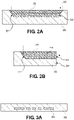
Figure 2A is a cross-sectional illustration of an electronic package with an embedded waveguide with a first sloped end and a second sloped end, in accordance with an embodiment. -
Figure 2B is a cross-sectional illustration of an electronic package with an embedded waveguide with a first sloped end and a second end at the edge of the package substrate, in accordance with an embodiment. -
Figures 3A-3F are cross-sectional illustrations depicting a process for forming an embedded waveguide, in accordance with an embodiment. -
Figure 4A is a cross-sectional illustration of an electronic package with a waveguide over the package substrate, in accordance with an embodiment. -
Figure 4B is a cross-sectional illustration of an electronic package with a waveguide over the package substrate and an end at the edge of the package substrate, in accordance with an embodiment. -
Figures 5A-5D are cross-sectional illustrations depicting a process for forming a waveguide over a package substrate, in accordance with an embodiment. -
Figure 6A is a cross-sectional illustration of an embedded waveguide with a reflective cladding, in accordance with an embodiment. -
Figure 6B is a cross-sectional illustration of an embedded waveguide with a reflective cladding that has an end at the edge of the package substrate, in accordance with an embodiment. -
Figures 7A-7C are cross-sectional illustrations depicting a process for forming a waveguide in a package substrate, in accordance with an embodiment. -
Figure 8A is a cross-sectional illustration of an embedded waveguide with reflective structures at opposite ends of the waveguide, in accordance with an embodiment. -
Figure 8B is a cross-sectional illustration of an embedded waveguide with a reflective structure at a first end and a second end at an edge of the package substrate, in accordance with an embodiment. -
Figures 9A-9I are cross-sectional illustrations depicting a process for forming an embedded waveguide with first and second reflective structures, in accordance with an embodiment. -
Figure 10A is a cross-sectional illustration of an embedded waveguide with reflective structures on opposite ends and a reflective cladding, in accordance with an embodiment. -
Figure 10B is a cross-sectional illustration of an embedded waveguide with a reflective structure at one end and a second end at an edge of the package substrate, in accordance with an embodiment. -
Figures 11A-11F are cross-sectional illustrations depicting a process for forming an embedded waveguide with reflective structures and a reflective cladding, in accordance with an embodiment. -
Figure 12A is a cross-sectional illustration of an embedded waveguide with a first reflective structure and a second reflective structure, in accordance with an embodiment. -
Figure 12B is a cross-sectional illustration of an embedded waveguide with a reflective structure at a first end and a second end at an edge of the package substrate, in accordance with an embodiment. -
Figures 13A-13H are cross-sectional illustrations depicting a process for forming an embedded waveguide with a first reflective structure and a second reflective structure, in accordance with an embodiment. -
Figure 14A is a cross-sectional illustration of an embedded waveguide with a reflective cladding, in accordance with an embodiment. -
Figure 14B is a cross-sectional illustration of an embedded waveguide with a reflective cladding that ends at an edge of the package substrate, in accordance with an embodiment. -
Figures 15A-15F are cross-sectional illustrations depicting a process for forming an embedded waveguide, in accordance with an embodiment. -
Figure 16A is a plan view illustration of an array of optical waveguides in a package substrate, in accordance with an embodiment. -
Figure 16B is a plan view illustration of a waveguide plane in a package substrate, in accordance with an embodiment. -
Figure 17 is a schematic of a computing device built in accordance with an embodiment. - Described herein are optical waveguide architectures to provide chip-to-chip communications, in accordance with various embodiments. In the following description, various aspects of the illustrative implementations will be described using terms commonly employed by those skilled in the art to convey the substance of their work to others skilled in the art. However, it will be apparent to those skilled in the art that the present invention may be practiced with only some of the described aspects. For purposes of explanation, specific numbers, materials and configurations are set forth in order to provide a thorough understanding of the illustrative implementations. However, it will be apparent to one skilled in the art that the present invention may be practiced without the specific details. In other instances, well-known features are omitted or simplified in order not to obscure the illustrative implementations.
- Various operations will be described as multiple discrete operations, in turn, in a manner that is most helpful in understanding the present invention, however, the order of description should not be construed to imply that these operations are necessarily order dependent. In particular, these operations need not be performed in the order of presentation.
- As noted above, embedded optical waveguides within a package substrate currently have significant optical losses due to alignment offsets created as a result of multiple patterning operations. Accordingly, embodiments disclosed herein include self-aligned reflective surfaces on opposite ends of the optical waveguide. In an embodiment, the optical waveguide provides a lateral path for routing signals, and the reflective surfaces allow for coupling with dies positioned above the package substrate. Due to the self-aligned nature of the reflective surfaces, optical losses are minimized.
- In some embodiments, the optical waveguide is over the package substrate. That is, the optical waveguide may be between the dies and the package substrate. In other embodiments, the optical waveguide is at least partially embedded in the package substrate. At least partially embedded may refer to a waveguide that has a bottom surface and sidewall surfaces covered by the package substrate, while a top surface of the waveguide is exposed to the atmosphere. In yet another embodiment, the optical waveguide is fully embedded in the package substrate, so that all surfaces along a length of the waveguide are covered by the package substrate.
- In an embodiment, the waveguides may comprise a high index of refraction material. For example, the index of refraction may be greater than 1.0. In other embodiments, the waveguides may comprise air. For example, a reflective cladding may surround a void in the package substrate, and the optical signal propagates through the void without any solid material along the optical path.
- In an embodiment, the reflective surfaces may be part of the optical waveguide. For example, differences in index of refraction may allow for a complete reflection of the signal at the ends of the waveguide. In other embodiments, reflective structures are provided at the ends of the waveguide. The reflective structures may have unique structures due to the self-aligned process. For example, the reflective structures may comprise trapezoidal shaped cross-sections with a triangular notch along a bottom surface. In other embodiments, the reflective structures may comprise parallelogram shaped cross-sections.
- Referring now to
Figure 1A , a cross-sectional illustration of anelectronic system 100 is shown, in accordance with an embodiment. In an embodiment, theelectronic system 100 may comprise a board 101 (such as a printed circuit board (PCB). Apackage substrate 102 is coupled to the board by interconnects 103. While shown as solder balls, it is to be appreciated that theinterconnects 103 may comprise any interconnect architecture, such as sockets or the like. In an embodiment, a pair of dies 110A and 110B are provided over thepackage substrate 102. First level interconnects (FLIs) 104 may couple thepackage substrate 102 to the dies 110A and 110B. - In an embodiment, an optical waveguide 120 (sometimes referred to as simply "
waveguide 120") is at least partially embedded in thepackage substrate 102. Thewaveguide 120 comprises afirst end 121 and asecond end 122. Thefirst end 121 is provided below the first die 110A and thesecond end 122 is provided below the second die 110B. In an embodiment,photonics regions 112 on the first die 110A and the second die 110B are directly over thefirst end 121 and thesecond end 122 of thewaveguide 120. As such, an optical signal (represented by the dashed line) can be sent between the first die 110A and the second die 110B. - In an embodiment, the
first end 121 and thesecond end 122 have sloped surfaces. As such, the direction of the optical signal can be changed from vertical to horizontal. In an embodiment, the sloped surfaces are approximately 45°, though it is to be appreciated that other angles may also be used. The reflection of thefirst end 121 and thesecond end 122 may be the result of mismatches in the index of refraction between thewaveguide 120 and thepackage substrate 102. For example, a material with an index of refraction greater than that of the package substrate may be used in order to provide total internal reflection at thefirst end 121 and thesecond end 122. In other embodiments (as will be described in greater detail below) the reflection at thefirst end 121 and thesecond end 122 may be made by reflective structures that are self-aligned to thewaveguide 120. - Referring now to
Figure 1B , a cross-sectional illustration of anelectronic system 100 is shown, in accordance with an additional embodiment. Theelectronic system 100 may be substantially similar to theelectronic system 100 described inFigure 1A , with the exception of the placement of thewaveguide 120. Instead of being embedded in thepackage substrate 102, thewaveguide 120 is provided between the dies 110A and 110B and thepackage substrate 102. In such an embodiment, thewaveguide 120 comprises an index of refraction material that is higher than air in order to provide the total internal reflection needed to rout optical signals from the first die 110A to the second die 110B. - Referring now to
Figure 2A , a cross-sectional illustration of anoptical waveguide 220 partially embedded in apackage substrate 202 is shown, in accordance with an embodiment. Thewaveguide 220 may have a bottom surface and sidewall surfaces that are contacted by thepackage substrate 202. A top surface of thewaveguide 220 may be exposed to the atmosphere. In an embodiment, theoptical waveguide 220 comprises a high index of refraction material, such as high index polymers or dielectrics. Particularly, the index of refraction of thewaveguide 220 is higher than the index of refraction of the surroundingpackage substrate 202 and atmosphere. - Due to the differences in the index of refraction, total internal reflection is provided when an
optical signal 225 reaches thefirst end 221 and thesecond end 222 of thewaveguide 220. Thewaveguide 220 may be patterned with an angled patterning process. As such, thefirst end 221 and thesecond end 222 may be sloped in order to redirect theoptical signal 225 vertically to allow communication between overlying dies (not shown). Since thefirst end 221 and thesecond end 222 are patterned during the patterning to form thewaveguide 220, thefirst end 221 and thesecond end 222 may be referred to as being self-aligned. A more detailed description of the angled patterning process is provided below. - Referring now to
Figure 2B , a cross-sectional illustration of anoptical waveguide 220 in apackage substrate 202 is shown, in accordance with an additional embodiment. Theoptical waveguide 220 may comprise afirst end 221 that is sloped and asecond end 222 that is vertical. Thesecond end 222 may be substantially coplanar with anedge 207 of thepackage substrate 202. In such an embodiment, theoptical signal 225 may be routed off thepackage substrate 202 to another device. In an embodiment, the materials for theoptical waveguide 220 andpackage substrate 202 inFigure 2B may be substantially similar to those described above with respect toFigure 2A . - Referring now to
Figures 3A-3F , a series of cross-sectional illustrations depicting a process for forming an embedded waveguide similar to the one shown inFigure 2A is shown, in accordance with an embodiment. - Referring now to
Figure 3A , a cross-sectional illustration of apackage substrate 302 is shown, in accordance with an embodiment. Thepackage substrate 302 may comprise a plurality of laminated dielectric layers withconductive routing 308. Thepackage substrate 302 may be cored or coreless. While a single layer ofconductive routing 308 is shown, it is to be appreciated that a plurality of conductive routing, vias, pads, etc. may be provided in thepackage substrate 302. - Referring now to
Figure 3B , a cross-sectional illustration of thepackage substrate 302 after a photo-imageable dielectric (PID) 331 is disposed over thepackage substrate 302 is shown, in accordance with an embodiment. ThePID 331 may be disposed with any suitable process, such as lamination. - Referring now to
Figure 3C , a cross-sectional illustration of thepackage substrate 302 after a first exposure is shown, in accordance with an embodiment. In an embodiment, amask 340 may be used to cover a portion of thePID 331. Afirst exposure 341 is used to expose portions of thePID 331 to form exposedPID 332. Thefirst exposure 341 may be an angled exposure. As such, the unexposed portion of thePID 331 may have a parallelogram shape. - Referring now to
Figure 3D , a cross-sectional illustration of thepackage substrate 302 after a second exposure is shown, in accordance with an embodiment. In an embodiment, thesecond exposure 342 may be done at an angle that mirrors the angle of thefirst exposure 341. As a result, the unexposed portions of thePID 331 may have a trapezoidal shape. It is to be appreciated that while two different exposures are made of thePID 331, themask 340 may not move between the different exposures. - Referring now to
Figure 3E , a cross-sectional illustration of thepackage substrate 302 after the unexposed portions of thePID 331 are removed is shown, in accordance with an embodiment. In an embodiment, the unexposed portions may be removed with a developing process to form atrench 333. Removal of the unexposed portions of thePID 331 results in the exposure of a firstsloped surface 334 and a secondsloped surface 335 at opposite ends of thetrench 333. - Referring now to
Figure 3F , a cross-sectional illustration of thepackage substrate 302 after anoptical waveguide 320 is disposed into thetrench 333 is shown, in accordance with an embodiment. In an embodiment, theoptical waveguide 320 comprises a high index of refraction material. Particularly, the index of refraction of theoptical waveguide 320 is higher than the index of refraction of thePID 332 and thepackage substrate 302. Theoptical waveguide 320 comprises afirst end 321 over thesurface 334 and asecond end 322 over thesurface 335. - Referring now to
Figure 4A , a cross-sectional illustration of anoptical waveguide 420 that is disposed over a package substrate is shown, in accordance with an embodiment. In an embodiment, alayer 451 with a low index of refraction material is provided under thewaveguide 420. Thelayer 451 may be disposed over the package substrate (not shown). For example, thelayer 451 may comprise SiO2 or SiN in some embodiments. - In an embodiment, the
waveguide 420 comprises a high index of refraction material. As such, anoptical signal 425 can be retained within thewaveguide 420 using total internal reflection. In a particular embodiment, thewaveguide 420 is a developed PID material. That is, thewaveguide 420 may be the result of a patterning process. Theoptical signal 425 may reflect off of afirst end 421 and asecond end 422 in order to rout theoptical signal 425 vertically to overlying dies (not shown). - Referring now to
Figure 4B , a cross-sectional illustration of anoptical waveguide 420 is shown, in accordance with an additional embodiment. In an embodiment, theoptical waveguide 420 includes afirst end 421 that is sloped and asecond end 422 that is vertical. Thesecond end 422 may be substantially coplanar with anedge 407 of the layer 451 (and the package substrate (not shown)). Similar to the embodiment inFigure 4A , theoptical waveguide 420 is provided above the package substrate instead of being embedded in the package substrate. The materials of theoptical waveguide 420 and thelayer 451 inFigure 4B may be substantially similar to the materials described above with respect toFigure 4A . - Referring now to
Figures 5A-5D , a series of cross-sectional illustrations depicting a process for forming an optical waveguide on apackage substrate 502 is shown, in accordance with an embodiment. - Referring now to
Figure 5A , a cross-sectional illustration of apackage substrate 502 is shown, in accordance with an embodiment. In an embodiment, thepackage substrate 502 may be substantially similar to thepackage substrate 302 described above. For example, thepackage substrate 502 may comprise dielectric layers withconductive routing 508. In an embodiment, alayer 551 with a low refractive index is provided over thepackage substrate 502. For example, thelayer 551 may comprise SiO2 or SiN. Thelayer 551 may be deposited with a sputtering process, or any other suitable material deposition process. In an embodiment, aPID 531 is provided over thelayer 551. ThePID 531 may be a positive resist material. That is, exposed regions of thePID 531 will be developed away. - Referring now to
Figure 5B , a cross-sectional illustration of thepackage substrate 502 after a first exposure is shown, in accordance with an embodiment. In an embodiment, amask 540 may be used to cover a portion of thePID 531. Afirst exposure 541 is used to expose portions of thePID 531 to form exposedPID 532. Thefirst exposure 541 may be an angled exposure. As such, the unexposed portion of thePID 531 may have a parallelogram shape. - Referring now to
Figure 5C , a cross-sectional illustration of thepackage substrate 502 after a second exposure is shown, in accordance with an embodiment. In an embodiment, thesecond exposure 542 may be done at an angle that mirrors the angle of thefirst exposure 541. As a result, the unexposed portions of thePID 531 may have a trapezoidal shape. It is to be appreciated that while two different exposures are made of thePID 531, themask 540 may not move between the different exposures. - Referring now to
Figure 5D , a cross-sectional illustration of thepackage substrate 502 after the exposed portions of thePID 532 are developed and removed is shown, in accordance with an embodiment. As shown, the residual portions of theunexposed PID 531 have a trapezoidal shape that can be used as anoptical waveguide 520. Thewaveguide 520 comprises afirst end 521 with a sloped surface and asecond end 522 with a sloped surface. - Referring now to
Figure 6A , a cross-sectional illustration of anoptical waveguide 620 in apackage substrate 602 is shown, in accordance with an additional embodiment. In an embodiment, thewaveguide 620 may include areflective cladding 623. Thereflective cladding 623 may be provided between a low loss material of thewaveguide 620 and thepackage substrate 602. The use of areflective cladding 623 allows for lower index of refraction materials to be used for thewaveguide 620. Instead of providing an index of refraction that is higher than that of thepackage substrate 602, all that is required is that the index of refraction be higher than that of the atmosphere (e.g., greater than approximately 1.0). As such, the material for the waveguide may be selected based on loss characteristics. For example, the material of thewaveguide 620 may be a dielectric without any fillers. - In an embodiment, the
reflective cladding 623 may be provided over a bottom surface of thewaveguide 620 and over thefirst end 621 and thesecond end 622. As such, an incomingoptical signal 625 may be propagated through thewaveguide 620 by reflecting off of thereflective cladding 623 on thefirst end 621 and thesecond end 622. In an embodiment, thereflective cladding 623 may comprise a thin, smooth layer, such as a material deposited with an electroless plating process or a liquid metal ink (LMI) process. For example, thereflective cladding 623 may comprise copper, gold, silver, palladium, or the like. - Referring now to
Figure 6B , a cross-sectional illustration of anoptical waveguide 620 on apackage substrate 602 is shown, in accordance with an additional embodiment. In an embodiment, theoptical waveguide 620 comprises areflective cladding 623 between theoptical waveguide 620 and thepackage substrate 602. In an embodiment, afirst end 621 has a sloped surface and asecond end 622 has a vertical surface. Thesecond end 622 may be substantially coplanar with anedge 607 of thepackage substrate 602. In an embodiment, the materials of theoptical waveguide 620 and thereflective cladding 623 may be substantially similar to those described above with respect toFigure 6A . - Referring now to
Figures 7A-7C , a series of cross-sectional illustrations depicting a process for forming an optical waveguide in a package substrate is shown, in accordance with an embodiment. - Referring now to
Figure 7A , a cross-sectional illustration of apackage substrate 702 is shown, in accordance with an embodiment. In an embodiment, the processing to get to the structure shown inFigure 7A may be substantially similar to the processing operations described above inFigures 3A-3E , and will not be repeated here. Particularly, an angled patterning process is used to form aPID 732 with atrench 733. Thetrench 733 may comprise a firstsloped sidewall 734 and a secondsloped sidewall 735. - Referring now to
Figure 7B , a cross-sectional illustration of thepackage substrate 702 after areflective cladding 723 is deposited is shown, in accordance with an embodiment. In an embodiment, thereflective cladding 723 may be deposited with an electroless plating process or any other conformal deposition process that can provide a smooth surface. In an embodiment, thereflective cladding 723 may comprise copper, gold, silver, palladium, or the like. - Referring now to
Figure 7C , a cross-sectional illustration of thepackage substrate 702 after awaveguide 720 is disposed in thetrench 733 is shown, in accordance with an embodiment. In an embodiment, thewaveguide 720 has afirst end 721 and asecond end 722. Thefirst end 721 and thesecond end 722 are sloped surfaces in order to allow for the optical signal to be routed vertically to overlying dies (not shown). - Referring now to
Figure 8A , a cross-sectional illustration of anoptical waveguide 820 in apackage substrate 802 is shown, in accordance with an embodiment. In an embodiment, theoptical waveguide 820 comprises afirst end 821 and asecond end 822. Thefirst end 821 and thesecond end 822 may be adjacent toreflective structures 861. Theoptical signal 825 reflects off of thereflective structures 861 to be routed to overlying dies (not shown). In an embodiment, theoptical waveguide 820 may comprise a material with a high index of refraction, such as materials described above. - In an embodiment, the
waveguide 820 is fully embedded in thepackage substrate 802. Particularly, adielectric layer 808 is disposed over a top surface of thewaveguide 820. That is, dielectric material from thepackage substrate 802 and thedielectric layer 808 may be provided over the bottom surface and a portion of the top surface of thewaveguide 620. Accordingly, embodiments may include burying thewaveguide 820 in any layer of thepackage substrate 802. - In an embodiment, the
reflective structures 861 may have trapezoidal shaped cross-sections with atriangular notch 862 on a bottom surface. Thenotch 862 may be filled by dielectric material, or may remain as a void in the package. The novel shape of thereflective structures 861 are a result of patterning processes, which will be described in greater detail below. Thereflective structures 861 may be copper or other reflective material. - Referring now to
Figure 8B , a cross-sectional illustration of anoptical waveguide 820 on apackage substrate 802 is shown, in accordance with an embodiment. In an embodiment, thewaveguide 820 comprises afirst end 821 and asecond end 822. Thefirst end 821 is adjacent to areflective structure 861 and thesecond end 822 is substantially coplanar with anedge 807 of thepackage substrate 802. In an embodiment, thereflective structure 861 may be substantially similar to the reflective structures described above inFigure 8A . Thewaveguide 820 may comprise a material with a high index of refraction. - Referring now to
Figures 9A-9I a series of cross-sectional illustrations depicting a process for forming an optical waveguide in apackage substrate 902 is shown, in accordance with an embodiment. - Referring now to
Figure 9A , a cross-sectional illustration of apackage substrate 902 with a positive resistlayer 965 is shown, in accordance with an embodiment. In an embodiment, the resistlayer 965 may be deposited with any suitable deposition process. - Referring now to
Figure 9B , a cross-sectional illustration of the package substrate after a first exposure of the resistlayer 965 is made. In an embodiment, the exposure may be an angled patterning using a greyscale mask (not shown). As shownarrows 969 may be a high dose andarrow 968 may be a low dose. Thehigh dose areas 967 are shown in a first shading, and the low dose area is shown with asecond shading 966. - Referring now to
Figure 9C , a cross-sectional illustration of the package substrate after a second exposure of the resistlayer 965 is made. The exposure may be an angled patterning (in a direction opposite from the first patterning) using a greyscale mask. As shown, the second patterning overlays the first pattern to form a low dose region that is a trapezoidal shape. Thehigh dose regions 967 have trapezoidal shapes with triangular notches oflow dose regions 966 along a bottom surface. It is to be appreciated that thelow dose region 966 may get a double exposure. However, so long as there is a sufficient delta between thehigh dose regions 967 and thelow dose regions 966 then the subsequent developing processes will be able to be executed properly. - Referring now to
Figure 9D , a cross-sectional illustration of thepackage substrate 902 after a first developing process is shown, in accordance with an embodiment. In an embodiment, the first developing process is a fast develop that only removes thehigh dose regions 967. As shown,openings 963 are provided between the unexposed regions of the resistlayer 965 and thelow dose regions 966. - Referring now to
Figure 9E , a cross-sectional illustration of thepackage substrate 902 after a plating process is shown, in accordance with an embodiment. The plating may result inreflective structures 961 being formed in theopenings 963. The reflective structures have a trapezoidal shaped cross-sections with a triangular notch in the bottom surfaces. In an embodiment, thereflective structures 961 may comprise copper or the like. - Referring now to
Figure 9F , a cross-sectional illustration of thepackage substrate 902 after a second developing process is shown, in accordance with an embodiment. The second development process may be a longer develop in order to remove thelow dose regions 966. Removal of thelow dose regions 966 may result in the formation of atrench 964 between thereflective structures 961. In an embodiment, thenotches 962 in thereflective structures 961 may be voids in some embodiments. - Referring now to
Figure 9G , a cross-sectional illustration of thepackage substrate 902 after a high index ofrefraction material 919 is disposed is shown, in accordance with an embodiment. The high index ofrefraction material 919 may be deposited with a conformal deposition process, such as a spray coating or a sputtering process. In some embodiments, a hydrophobic treatment of the resist 965 may be made prior to deposition of the material 919 to prevent the material 919 from sticking to the resist 965. In an embodiment, thematerial 919 may be a high index polymer or dielectric. - Referring now to
Figure 9H , a cross-sectional illustration of thepackage substrate 902 after adielectric layer 908 is laminated and a planarization process is done is shown, in accordance with an embodiment. Thedielectric layer 908 may be laminated over thematerial 919 and the planarization process recesses thedielectric layer 908 and the material 919 to expose the top surfaces of thereflective structures 961. The recessing results in the formation of theoptical waveguide 920. Thewaveguide 920 comprises afirst end 921 and asecond end 922. Thefirst end 921 and thesecond end 922 are adjacent and contacting thereflective structures 961. After the planarization process, the resist 965 may be stripped, as shown inFigure 9H . - Referring now to
Figure 9I , a cross-sectional illustration of thepackage substrate 902 after an additionaldielectric layer 908 is laminated is shown, in accordance with an embodiment. As shown, thedielectric layer 908 covers the edge surfaces of thereflective structures 961 opposite from thewaveguide 920. In an embodiment, a planarization process may be used to expose the top surfaces of thereflective structures 961 after thedielectric layer 908 is laminated. In the illustrated embodiments, thenotches 962 may be filled with dielectric material or thenotches 962 may define a void in the package. - Referring now to
Figure 10A , a cross-sectional illustration of an electronic package with awaveguide 1020 embedded in apackage substrate 1002 is shown, in accordance with an embodiment. In an embodiment, thewaveguide 1020 may comprise areflective cladding 1023. Thereflective cladding 1023 may be copper or the like. In an embodiment, thewaveguide 1020 may be air within thereflective cladding 1023. Afirst end 1021 of thewaveguide 1020 may be adjacent to areflective structure 1061, and thesecond end 1022 of thewaveguide 1020 may be adjacent to areflective structure 1061. Thereflective structures 1061 may have trapezoidal shaped cross-sections with atriangular notch 1062 formed in a bottom surface. In an embodiment, thereflective structures 1061 route anoptical signal 1025 from within thewaveguide 1020 up to overlying dies (not shown). In an embodiment, adielectric layer 1008 may surround surfaces of thereflective structures 1061 opposite from thewaveguide 1020. - Referring now to
Figure 10B , a cross-sectional illustration of awaveguide 1020 is shown, in accordance with an additional embodiment. Instead of a pair ofreflective structures 1061, only a singlereflective structure 1061 is provided adjacent to thefirst end 1021. Thesecond end 1022 of thewaveguide 1020 is substantially coplanar with anedge 1007 of thepackage substrate 1002. While referred to as thesecond end 1022, it is to be appreciated that thewaveguide 1020 may be air filled between thereflective cladding 1023, and that there may not be a solid surface at thesecond end 1022. - Referring now to
Figures 11A-11F , a series of cross-sectional illustrations depicting a process for forming a waveguide in a package substrate is shown, in accordance with an embodiment. In an embodiment, the structure inFigure 11A may be formed using processing operations similar to those described above inFigures 9A-9E , and will not be repeated here. - Referring now to
Figure 11A , a cross-sectional illustration of a structure for forming an embedded waveguide is shown, in accordance with an embodiment. The structure comprises apackage substrate 1102 with a patterned resistlayer 1165. At this point in the process flow, the high dose regions of the positive resistlayer 1165 have been removed andreflective structures 1161 have been formed. Thelow dose regions 1166 of the positive resistlayer 1165 remain at this point in the process flow. - Referring now to
Figure 11B , a cross-sectional illustration of thepackage substrate 1102 after thelow dose regions 1166 are removed to form atrench 1164 and a portion of areflective cladding 1123 is formed is shown, in accordance with an embodiment. Removal of thelow dose regions 1166 may also formnotches 1162 that are air voids in a bottom surface of thereflective structures 1161. Thereflective cladding 1123 may form a bottom surface of the waveguide. Thereflective cladding 1123 may comprise copper. Additionally, thereflective cladding 1123 may directly couple the tworeflective structures 1161 together. - Referring now to
Figure 11C , a cross-sectional illustration of thepackage substrate 1102 after a thermallydecomposable layer 1180 is disposed over the exposed surfaces is shown, in accordance with an embodiment. In an embodiment, the thermallydecomposable layer 1180 comprises a material that can be removed at elevated temperatures. In an embodiment, the thermallydecomposable layer 1180 is deposited with a conformal process, such as a spray coating process. - Referring now to
Figure 11D , a cross-sectional illustration of thepackage substrate 1102 after a dielectric lamination and planarization process is shown, in accordance with an embodiment. In an embodiment, thedielectric layer 1108 is disposed over the thermallydecomposable layer 1180. A planarization process may then be implemented to expose the top surfaces of thereflective structures 1161. After the planarization process, the resistlayer 1165 may be stripped. - Referring now to
Figure 11E , a cross-sectional illustration of thepackage substrate 1102 after anadditional dielectric layer 1108 is laminated to cover the outside surfaces of thereflective structures 1161 and the thermallydecomposable layer 1180 is removed is shown, in accordance with an embodiment. An additional planarization process may be done between thedielectric layer 1108 lamination and the removal of the thermallydecomposable layer 1180. The removal of the thermallydecomposable layer 1180 results in the formation of a void that is used as thewaveguide 1120. As shown, a portion of thedielectric layer 1108 appears floating over thewaveguide 1120. However, it is to be appreciated that the floating portion is supported out of the plane ofFigure 11E . - Referring now to
Figure 11F , a cross-sectional illustration of thepackage substrate 1102 after a top portion of thecladding 1123 is formed is shown, in accordance with an embodiment. In an embodiment, the top portion of thecladding 1123 over the floating portion of the dielectric 1108 may be done with an electroless plating process or the like. In some embodiments, the top portion of thecladding 1123 may be omitted. Additionally, a high index of refraction liquid material may be dispensed into thewaveguide 1120 in some embodiments. - Referring now to
Figure 12A , a cross-sectional illustration of anoptical waveguide 1220 in apackage substrate 1202 is shown, in accordance with an embodiment. In an embodiment, theoptical waveguide 1220 comprises a high index of refraction material, such as a high index polymer or dielectric. In an embodiment, thewaveguide 1220 comprises afirst end 1221 and asecond end 1222. Thefirst end 1221 and thesecond end 1222 are adjacent toreflective structures first structure 1281 is a mirror image of thesecond structure 1282. Thereflective structures optical signal 1225 that passes through thewaveguide 1220 to overlying dies (not shown). In an embodiment, adielectric layer 1208 embeds thewaveguide 1220. Thedielectric layer 1208 may be considered as part of thepackage substrate 1202 in some embodiments. - Referring now to
Figure 12B , a cross-sectional illustration of apackage substrate 1202 with awaveguide 1220 is shown, in accordance with an additional embodiment. Thewaveguide 1220 is similar to thewaveguide 1220 inFigure 12A , with the exception of thesecond end 1222 ending at anedge 1207 of thepackage substrate 1202. There is also noreflective structure 1282 at thesecond end 1222 of thewaveguide 1220. - Referring now to
Figures 13A-13H , a series of cross-sectional illustrations depicting a process for forming an embedded waveguide is shown, in accordance with an embodiment. - Referring now to
Figure 13A , a cross-sectional illustration of apackage substrate 1302 is shown, in accordance with an embodiment. A resistlayer 1365 may be disposed over a top surface of thepackage substrate 1302. - Referring now to
Figure 13B , a cross-sectional illustration of thepackage substrate 1302 after the resistlayer 1365 is exposed is shown, in accordance with an embodiment. In an embodiment, the resist layer may be exposed using a two-photon-polymerization (2PP) variable exposure. This results in alow dose exposure 1368 andhigh dose exposures 1369. Thelow dose region 1366 may have a trapezoidal shape, and thehigh dose regions 1367 may have parallelogram shapes. The twohigh dose regions 1367 may be mirror images of each other. For a positive tone resist, such as diazoalkylquinone doped with a 2PP marker with a high 2P cross-section may be used to provide the 2PP variable exposure. - Referring now to
Figure 13C , a cross-sectional illustration after thehigh dose regions 1367 are removed with a first developing process is shown, in accordance with an embodiment. In an embodiment, the duration of the first developing process is short in order to ensure that none of thelow dose region 1366 is removed. Removal of thehigh dose regions 1367 results in the formation oftrenches 1363. - Referring now to
Figure 13D , a cross-sectional illustration of thepackage substrate 1302 afterreflective structures trenches 1363 is shown, in accordance with an embodiment. In an embodiment, thereflective structures reflective structures - Referring now to
Figure 13E , a cross-sectional illustration of thepackage substrate 1302 after thelow dose region 1366 is removed is shown, in accordance with an embodiment. Removal of thelow dose region 1366 results in the formation of atrench 1364 between thereflective structures - Referring now to
Figure 13F , a cross-sectional illustration of thepackage substrate 1302 after alayer 1319 with a high index of refraction is disposed over the exposed surfaces is shown, in accordance with an embodiment. In an embodiment, thelayer 1319 may be conformally deposited (e.g., with a spray coating or sputtering process). In some embodiments, a hydrophobic treatment is applied to the resistlayer 1365 to prevent deposition on the resistlayer 1365. - Referring now to
Figure 13G , a cross-sectional illustration of thepackage substrate 1302 after adielectric layer 1308 is deposited and planarized is shown, in accordance with an embodiment. In an embodiment, the planarization process exposes the top surfaces of thereflective structures layer 1319 to form thewaveguide 1320 between thereflective structures waveguide 1320 comprises afirst end 1321 next to thereflective structure 1381 and asecond end 1322 next to thereflective structure 1382. After the planarization process, the resistlayer 1365 may be removed. - Referring now to
Figure 13H , a cross-sectional illustration of thepackage substrate 1302 after anadditional dielectric layer 1308 is laminated and planarized is shown, in accordance with an embodiment. In an embodiment, theadditional dielectric layer 1308 covers the sidewall surfaces of thereflective structures waveguide 1320. - Referring now to
Figure 14A , a cross-sectional illustration of an embeddedwaveguide 1420 is shown, in accordance with an embodiment. In an embodiment, the structure comprises apackage substrate 1402. A pair ofreflective structures package substrate 1402. Thereflective structures reflective cladding 1423. In an embodiment, adielectric layer 1408 covers sidewall surfaces of thereflective structures - In an embodiment, a portion of the
dielectric layer 1408 may be above thewaveguide 1420. Thewaveguide 1420 may comprisecladding layers 1423 and be air filled. Thewaveguide 1420 has afirst end 1421 and asecond end 1422.Optical signals 1425 propagate along thewaveguide 1420 and reflect off of thereflective structures - Referring now to
Figure 14B , a cross-sectional illustration of an embeddedwaveguide 1420 is shown, in accordance with an additional embodiment. Thewaveguide 1420 inFigure 14B is similar to the waveguide inFigure 14A , with the exception of thesecond end 1422 ending at anedge 1407 of thepackage substrate 1402. That is, there is no secondreflective structure 1482 in the embodiment shown inFigure 14B . - Referring now to
Figures 15A-15F a series of cross-sectional illustrations depicting a process for forming an embedded waveguide is shown, in accordance with an embodiment. The structure shown inFigure 15A may be fabricated using processing operations substantially similar to those described above with respect toFigures 13A-13E , and will not be repeated here. - Referring now to
Figure 15A , a cross-sectional illustration of apackage substrate 1502 with a patterned resistlayer 1565 is shown, in accordance with an embodiment. Atrench 1564 may be formed in the patterned resistlayer 1565. In an embodiment, a firstreflective structure 1581 and a secondreflective structure 1582 are formed at edges of thetrench 1564. Thereflective structures reflective structures - Referring now to
Figure 15B , a cross-sectional illustration of thepackage substrate 1502 after abottom cladding 1523 is disposed over thepackage substrate 1502 is shown, in accordance with an embodiment. Thebottom cladding 1523 may be copper or the like. Thebottom cladding 1523 connects the firstreflective structure 1581 to the secondreflective structure 1582. - Referring now to
Figure 15C , a cross-sectional illustration of the package substrate after a thermallydecomposable layer 1580 is disposed over exposed surfaces is shown, in accordance with an embodiment. The thermallydecomposable layer 1580 may be a material that decomposes at elevated temperatures. In an embodiment, the thermallydecomposable layer 1580 may be deposited with a spray coating process or the like. - Referring now to
Figure 15D , a cross-sectional illustration after a dielectric layer is laminated and a planarization process is implemented is shown, in accordance with an embodiment. In an embodiment, thedielectric layer 1508 is disposed over the thermallydecomposable layer 1580. The planarization process may be used to expose the top surfaces of thereflective structures layer 1565 may be stripped. - Referring now to
Figure 15E , a cross-sectional illustration of thepackage substrate 1502 after anadditional dielectric layer 1508 is laminated to cover the outside surfaces of thereflective structures decomposable layer 1580 is removed is shown, in accordance with an embodiment. An additional planarization process may be done between thedielectric layer 1508 lamination and the removal of the thermallydecomposable layer 1580. The removal of the thermallydecomposable layer 1580 results in the formation of a void that is used as thewaveguide 1520. As shown, a portion of thedielectric layer 1508 appears floating over thewaveguide 1520. However, it is to be appreciated that the floating portion is supported out of the plane ofFigure 15E . - Referring now to
Figure 15F , a cross-sectional illustration of thepackage substrate 1502 after a top portion of thecladding 1523 is formed is shown, in accordance with an embodiment. In an embodiment, the top portion of thecladding 1523 over the floating portion of the dielectric 1508 may be done with an electroless plating process or the like. In some embodiments, the top portion of thecladding 1523 may be omitted. Additionally, a high index of refraction liquid material may be dispensed into thewaveguide 1520 in some embodiments. In an embodiment, thewaveguide 1520 comprises afirst end 1521 adjacent to the firstreflective structure 1581 and asecond end 1522 adjacent to the secondreflective structure 1582. - Referring now to
Figure 16A , a plan view illustration of anelectronic package 1600 is shown, in accordance with an embodiment. As shown, an array ofoptical paths 16901-3 are provided across the surface of thepackage substrate 1602. While threeoptical paths 1690 are shown, it is to be appreciated that any number ofoptical paths 1690 may be used. In an embodiment, each of theoptical paths 1690 comprises a pair ofreflective structures 1661 and anoptical waveguide 1620. The horizontal portion of theoptical waveguide 1620 is below the surface of thepackage substrate 1602. - Referring now to
Figure 16B , a plan view illustration of anelectronic package 1600 is shown, in accordance with an additional embodiment. In an embodiment, awaveguide plane 1690 is provided. Thewaveguide plane 1690 includes widerreflective structure 1661 andwaveguide 1620. The extended width allows for multiple signals to be passed along thesingle waveguide plane 1690. Such an embodiment may be useful when light scattering within thewaveguide 1620 is negligible. -
Figure 17 illustrates acomputing device 1700 in accordance with one implementation of the invention. Thecomputing device 1700 houses aboard 1702. Theboard 1702 may include a number of components, including but not limited to aprocessor 1704 and at least onecommunication chip 1706. Theprocessor 1704 is physically and electrically coupled to theboard 1702. In some implementations the at least onecommunication chip 1706 is also physically and electrically coupled to theboard 1702. In further implementations, thecommunication chip 1706 is part of theprocessor 1704. - These other components include, but are not limited to, volatile memory (e.g., DRAM), non-volatile memory (e.g., ROM), flash memory, a graphics processor, a digital signal processor, a crypto processor, a chipset, an antenna, a display, a touchscreen display, a touchscreen controller, a battery, an audio codec, a video codec, a power amplifier, a global positioning system (GPS) device, a compass, an accelerometer, a gyroscope, a speaker, a camera, and a mass storage device (such as hard disk drive, compact disk (CD), digital versatile disk (DVD), and so forth).
- The
communication chip 1706 enables wireless communications for the transfer of data to and from thecomputing device 1700. The term "wireless" and its derivatives may be used to describe circuits, devices, systems, methods, techniques, communications channels, etc., that may communicate data through the use of modulated electromagnetic radiation through a non-solid medium. The term does not imply that the associated devices do not contain any wires, although in some embodiments they might not. Thecommunication chip 1706 may implement any of a number of wireless standards or protocols, including but not limited to Wi-Fi (IEEE 802.11 family), WiMAX (IEEE 802.16 family), IEEE 802.20, long term evolution (LTE), Ev-DO, HSPA+, HSDPA+, HSUPA+, EDGE, GSM, GPRS, CDMA, TDMA, DECT, Bluetooth, derivatives thereof, as well as any other wireless protocols that are designated as 3G, 4G, 5G, and beyond. Thecomputing device 1700 may include a plurality ofcommunication chips 1706. For instance, afirst communication chip 1706 may be dedicated to shorter range wireless communications such as Wi-Fi and Bluetooth and asecond communication chip 1706 may be dedicated to longer range wireless communications such as GPS, EDGE, GPRS, CDMA, WiMAX, LTE, Ev-DO, and others. - The
processor 1704 of thecomputing device 1700 includes an integrated circuit die packaged within theprocessor 1704. In some implementations of the invention, the integrated circuit die of the processor may be communicatively coupled to an additional die through a self-aligned optical waveguide, in accordance with embodiments described herein. The term "processor" may refer to any device or portion of a device that processes electronic data from registers and/or memory to transform that electronic data into other electronic data that may be stored in registers and/or memory. - The
communication chip 1706 also includes an integrated circuit die packaged within thecommunication chip 1706. In accordance with another implementation of the invention, the integrated circuit die of the communication chip may be communicatively coupled to an additional die through a self-aligned optical waveguide, in accordance with embodiments described herein. - The above description of illustrated implementations of the invention, including what is described in the Abstract, is not intended to be exhaustive or to limit the invention to the precise forms disclosed. While specific implementations of, and examples for, the invention are described herein for illustrative purposes, various equivalent modifications are possible within the scope of the invention, as those skilled in the relevant art will recognize.
- These modifications may be made to the invention in light of the above detailed description. The terms used in the following claims should not be construed to limit the invention to the specific implementations disclosed in the specification and the claims. Rather, the scope of the invention is to be determined entirely by the following claims, which are to be construed in accordance with established doctrines of claim interpretation.
- Example 1: an electronic package, comprising: a package substrate; a first die over the package substrate; a second die over the package substrate; and an optical waveguide on the package substrate, wherein a first end of the optical waveguide is below the first die and a second end of the optical waveguide is below the second die, and wherein the optical waveguide communicatively couples the first die to the second die.
- Example 2: the electronic package of Example 1, wherein the first end of the optical waveguide and the second end of the optical waveguide comprise sloped surfaces.
- Example 3: the electronic package of Example 1 or Example 2, wherein the optical waveguide comprises a material with an index of refraction greater than 1.0.
- Example 4: the electronic package of Examples 1-3, wherein the optical waveguide comprises air.
- Example 5: the electronic package of Example 4, wherein the optical waveguide comprises a reflective cladding around the air.
- Example 6: the electronic package of Examples 1-5, wherein the optical waveguide is above the package substrate.
- Example 7: the electronic package of Examples 1-6, wherein a top surface of the optical waveguide contacts air or an index matching fluid or gel.
- Example 8: the electronic package of Examples 1-7, further comprising: a first reflective structure at the first end of the optical waveguide and a second reflective structure at the second end of the optical waveguide.
- Example 9: the electronic package of Example 8, wherein the first reflective structure and the second reflective structure have trapezoidal cross-sections with a triangular notch in a bottom surface.
- Example 10: the electronic package of Example 9, wherein the first reflective structure is connected to the second reflective structure by a reflective layer.
- Example 11: the electronic package of Example 8, wherein the first reflective structure and the second reflective structure have parallelogram shaped cross-sections.
- Example 12: the electronic package of Example 11, wherein the first reflective structure is a mirror image of the second reflective structure.
- Example 13: an electronic package, comprising: a package substrate; and an optical waveguide embedded in the package substrate, wherein the optical waveguide comprises a first end with a sloped surface.
- Example 14: the electronic package of Example 13, wherein a reflective structure is adjacent to the first end.
- Example 15: the electronic package of Example 14, wherein the reflective structure comprises a trapezoidal cross-section.
- Example 16: the electronic package of Example 15, wherein a triangular notch is provided on a bottom surface of the reflective structure.
- Example 17: the electronic package of Example 16, wherein the triangular notch defines a void in the package substrate.
- Example 18: the electronic package of Example 14, wherein the reflective structure comprises a parallelogram shaped cross-section.
- Example 19: the electronic package of Examples 13-18, wherein the optical waveguide comprises a material with an index of refraction greater than 1.0.
- Example 20: the electronic package of Examples 13-19, wherein the optical waveguide comprises air.
- Example 21: the electronic package of Example 20, wherein the optical waveguide further comprises a reflective cladding.
- Example 22: the electronic package of Examples 13-21, wherein a second end of the optical waveguide is at an edge of the package substrate.
- Example 23: an electronic system, comprising: a board; a package substrate attached to the board; a first die over the package substrate; a second die over the package substrate; and an optical waveguide on the package substrate, wherein the optical waveguide comprises a first end and a second end, and wherein the first end and the second end are sloped to allow for communicative coupling between the first die and the second die.
- Example 24: the electronic system of Example 23, further comprising: a first reflective structure adjacent to the first end and a second reflective structure adjacent to the second end, wherein the first reflective structure is a mirror image of the second reflective structure.
- Example 25: the electronic system of Example 23 or Example 24, wherein the optical waveguide comprises a material with an index of refraction greater than 1.0.
Claims (15)
- An electronic package, comprising:a package substrate;a first die over the package substrate;a second die over the package substrate; andan optical waveguide on the package substrate, wherein a first end of the optical waveguide is below the first die and a second end of the optical waveguide is below the second die, and wherein the optical waveguide communicatively couples the first die to the second die.
- The electronic package of claim 1, wherein the first end of the optical waveguide and the second end of the optical waveguide comprise sloped surfaces.
- The electronic package of claim 1 or 2, wherein the optical waveguide comprises a material with an index of refraction greater than 1.0.
- The electronic package of claim 1, 2 or 3, wherein the optical waveguide comprises air.
- The electronic package of claim 4, wherein the optical waveguide comprises a reflective cladding around the air.
- The electronic package of claim 1, 2, 3, 4 or 5, wherein the optical waveguide is above the package substrate.
- The electronic package of claim 1, 2, 3, 4, 5 or 6, wherein a top surface of the optical waveguide contacts air or an index matching fluid or gel.
- The electronic package of claim 1, 2, 3, 4, 5, 6 or 7, further comprising:
a first reflective structure at the first end of the optical waveguide and a second reflective structure at the second end of the optical waveguide. - The electronic package of claim 8, wherein the first reflective structure and the second reflective structure have trapezoidal cross-sections with a triangular notch in a bottom surface.
- The electronic package of claim 9, wherein the first reflective structure is connected to the second reflective structure by a reflective layer.
- A method of fabricating an electronic package, the method comprising:coupling a first die and a package substrate;coupling a second die and the package substrate; andcoupling an optical waveguide and the package substrate, wherein a first end of the optical waveguide is below the first die and a second end of the optical waveguide is below the second die, and wherein the optical waveguide communicatively couples the first die to the second die.
- The method of claim 11, wherein the first end of the optical waveguide and the second end of the optical waveguide comprise sloped surfaces.
- The method of claim 11 or 12, wherein the optical waveguide comprises a material with an index of refraction greater than 1.0.
- The method of claim 11, 12 or 13, wherein the optical waveguide comprises air.
- The method of claim 14, wherein the optical waveguide comprises a reflective cladding around the air.
Applications Claiming Priority (1)
| Application Number | Priority Date | Filing Date | Title |
|---|---|---|---|
| US17/131,678 US20220196914A1 (en) | 2020-12-22 | 2020-12-22 | Waveguide with self-aligned mirror in package for long range chip-to-chip communications |
Publications (1)
| Publication Number | Publication Date |
|---|---|
| EP4020039A1 true EP4020039A1 (en) | 2022-06-29 |
Family
ID=77838716
Family Applications (1)
| Application Number | Title | Priority Date | Filing Date |
|---|---|---|---|
| EP21197529.7A Pending EP4020039A1 (en) | 2020-12-22 | 2021-09-17 | Waveguide with self-aligned mirror in package for long range chip-to-chip communications |
Country Status (3)
| Country | Link |
|---|---|
| US (1) | US20220196914A1 (en) |
| EP (1) | EP4020039A1 (en) |
| CN (1) | CN114664804A (en) |
Citations (6)
| Publication number | Priority date | Publication date | Assignee | Title |
|---|---|---|---|---|
| US20030228084A1 (en) * | 2002-06-06 | 2003-12-11 | Fujitsu Limited | Printed board unit for optical transmission and mounting method |
| KR100834648B1 (en) * | 2007-02-23 | 2008-06-02 | 삼성전자주식회사 | Optical and electrical hybrid board and fabricating method thereof |
| CN101344624A (en) * | 2008-07-17 | 2009-01-14 | 华中科技大学 | Optoelectronic combination printing circuit board with optical interconnection direct coupling between chips |
| WO2009096981A1 (en) * | 2008-01-31 | 2009-08-06 | Hewlett-Packard Development Company, L.P. | Optical taps for circuit board-mounted optical waveguides |
| US20100272388A1 (en) * | 2009-04-23 | 2010-10-28 | Im Young-Min | Photoelectric conversion module |
| US20160356961A1 (en) * | 2015-06-05 | 2016-12-08 | Dyi-chung Hu | Embedded optical fiber module |
-
2020
- 2020-12-22 US US17/131,678 patent/US20220196914A1/en active Pending
-
2021
- 2021-09-17 EP EP21197529.7A patent/EP4020039A1/en active Pending
- 2021-11-22 CN CN202111385797.8A patent/CN114664804A/en active Pending
Patent Citations (6)
| Publication number | Priority date | Publication date | Assignee | Title |
|---|---|---|---|---|
| US20030228084A1 (en) * | 2002-06-06 | 2003-12-11 | Fujitsu Limited | Printed board unit for optical transmission and mounting method |
| KR100834648B1 (en) * | 2007-02-23 | 2008-06-02 | 삼성전자주식회사 | Optical and electrical hybrid board and fabricating method thereof |
| WO2009096981A1 (en) * | 2008-01-31 | 2009-08-06 | Hewlett-Packard Development Company, L.P. | Optical taps for circuit board-mounted optical waveguides |
| CN101344624A (en) * | 2008-07-17 | 2009-01-14 | 华中科技大学 | Optoelectronic combination printing circuit board with optical interconnection direct coupling between chips |
| US20100272388A1 (en) * | 2009-04-23 | 2010-10-28 | Im Young-Min | Photoelectric conversion module |
| US20160356961A1 (en) * | 2015-06-05 | 2016-12-08 | Dyi-chung Hu | Embedded optical fiber module |
Also Published As
| Publication number | Publication date |
|---|---|
| US20220196914A1 (en) | 2022-06-23 |
| CN114664804A (en) | 2022-06-24 |
Similar Documents
| Publication | Publication Date | Title |
|---|---|---|
| US9028157B2 (en) | Efficient backside-emitting/collecting grating coupler | |
| US7135777B2 (en) | Devices having compliant wafer-level input/output interconnections and packages using pillars and methods of fabrication thereof | |
| TWI756368B (en) | Photonic chip and packaged photonic chip system | |
| TW201530205A (en) | Integrated optoelectronic module | |
| NL2029423B1 (en) | High bandwidth optical interconnection architectures | |
| KR102626836B1 (en) | Vertical optical via and method of fabrication | |
| JP2016180860A (en) | Semiconductor device and manufacturing method for the same | |
| EP4020039A1 (en) | Waveguide with self-aligned mirror in package for long range chip-to-chip communications | |
| EP4016150A1 (en) | Faraday rotator optical interconnects for optical insulator in semiconductor substrate packaging | |
| US20190295951A1 (en) | Lithographic cavity formation to enable emib bump pitch scaling | |
| EP4016151A1 (en) | Faraday rotator interconnect as a through-via configuration in a patch architecture | |
| CN105118843A (en) | Packaging structure and packaging method | |
| US11448822B2 (en) | Silicon-on-insulator chip structure with substrate-embedded optical waveguide and method | |
| US20230093438A1 (en) | Glass substrate embedded pic to pic and off-chip photonic communications | |
| US20240087971A1 (en) | Copper clad laminate (ccl) for plating pads within a glass cavity for glass core applications | |
| KR20240059600A (en) | PIC-to-PIC and off-chip photonic communication embedded in glass substrates | |
| US20240094469A1 (en) | Packages With Photonic Engines and Method of Forming the Same | |
| US20220404568A1 (en) | Package with optical waveguide in a glass core | |
| US20220196936A1 (en) | Bidirectional optical grating coupler with multiple light paths for testing photonics devices | |
| US20200064738A1 (en) | Method to achieve tilted patterning with a through resist thickness | |
| CN116314122A (en) | Low loss microstrip and stripline routing with blind-trench vias for high speed signal transmission on glass cores | |
| WO2022231641A1 (en) | Process integration solution for an optical component | |
| TW202310435A (en) | Coupling system | |
| CN117393496A (en) | Package and method of forming the same | |
| JP2002082242A (en) | Optical wiring layer, its manufacturing method, optoelectric wiring board and package board |
Legal Events
| Date | Code | Title | Description |
|---|---|---|---|
| PUAI | Public reference made under article 153(3) epc to a published international application that has entered the european phase |
Free format text: ORIGINAL CODE: 0009012 |
|
| STAA | Information on the status of an ep patent application or granted ep patent |
Free format text: STATUS: THE APPLICATION HAS BEEN PUBLISHED |
|
| AK | Designated contracting states |
Kind code of ref document: A1 Designated state(s): AL AT BE BG CH CY CZ DE DK EE ES FI FR GB GR HR HU IE IS IT LI LT LU LV MC MK MT NL NO PL PT RO RS SE SI SK SM TR |
|
| STAA | Information on the status of an ep patent application or granted ep patent |
Free format text: STATUS: REQUEST FOR EXAMINATION WAS MADE |
|
| 17P | Request for examination filed |
Effective date: 20221201 |
|
| RBV | Designated contracting states (corrected) |
Designated state(s): AL AT BE BG CH CY CZ DE DK EE ES FI FR GB GR HR HU IE IS IT LI LT LU LV MC MK MT NL NO PL PT RO RS SE SI SK SM TR |
|
| GRAP | Despatch of communication of intention to grant a patent |
Free format text: ORIGINAL CODE: EPIDOSNIGR1 |
|
| STAA | Information on the status of an ep patent application or granted ep patent |
Free format text: STATUS: GRANT OF PATENT IS INTENDED |
|
| INTG | Intention to grant announced |
Effective date: 20240301 |