EP4018487B1 - Wafer optical processing device and sintering furnace - Google Patents
Wafer optical processing device and sintering furnace Download PDFInfo
- Publication number
- EP4018487B1 EP4018487B1 EP20765395.7A EP20765395A EP4018487B1 EP 4018487 B1 EP4018487 B1 EP 4018487B1 EP 20765395 A EP20765395 A EP 20765395A EP 4018487 B1 EP4018487 B1 EP 4018487B1
- Authority
- EP
- European Patent Office
- Prior art keywords
- wafer
- light source
- optical processing
- source device
- processing device
- Prior art date
- Legal status (The legal status is an assumption and is not a legal conclusion. Google has not performed a legal analysis and makes no representation as to the accuracy of the status listed.)
- Active
Links
Images



Classifications
-
- H—ELECTRICITY
- H10—SEMICONDUCTOR DEVICES; ELECTRIC SOLID-STATE DEVICES NOT OTHERWISE PROVIDED FOR
- H10F—INORGANIC SEMICONDUCTOR DEVICES SENSITIVE TO INFRARED RADIATION, LIGHT, ELECTROMAGNETIC RADIATION OF SHORTER WAVELENGTH OR CORPUSCULAR RADIATION
- H10F71/00—Manufacture or treatment of devices covered by this subclass
- H10F71/128—Annealing
-
- H—ELECTRICITY
- H10—SEMICONDUCTOR DEVICES; ELECTRIC SOLID-STATE DEVICES NOT OTHERWISE PROVIDED FOR
- H10P—GENERIC PROCESSES OR APPARATUS FOR THE MANUFACTURE OR TREATMENT OF DEVICES COVERED BY CLASS H10
- H10P72/00—Handling or holding of wafers, substrates or devices during manufacture or treatment thereof
- H10P72/04—Apparatus for manufacture or treatment
- H10P72/0431—Apparatus for thermal treatment
- H10P72/0436—Apparatus for thermal treatment mainly by radiation
-
- H—ELECTRICITY
- H10—SEMICONDUCTOR DEVICES; ELECTRIC SOLID-STATE DEVICES NOT OTHERWISE PROVIDED FOR
- H10F—INORGANIC SEMICONDUCTOR DEVICES SENSITIVE TO INFRARED RADIATION, LIGHT, ELECTROMAGNETIC RADIATION OF SHORTER WAVELENGTH OR CORPUSCULAR RADIATION
- H10F71/00—Manufacture or treatment of devices covered by this subclass
- H10F71/10—Manufacture or treatment of devices covered by this subclass the devices comprising amorphous semiconductor material
- H10F71/107—Continuous treatment of the devices, e.g. roll-to roll processes or multi-chamber deposition
-
- H—ELECTRICITY
- H10—SEMICONDUCTOR DEVICES; ELECTRIC SOLID-STATE DEVICES NOT OTHERWISE PROVIDED FOR
- H10P—GENERIC PROCESSES OR APPARATUS FOR THE MANUFACTURE OR TREATMENT OF DEVICES COVERED BY CLASS H10
- H10P72/00—Handling or holding of wafers, substrates or devices during manufacture or treatment thereof
- H10P72/04—Apparatus for manufacture or treatment
- H10P72/0431—Apparatus for thermal treatment
- H10P72/0432—Apparatus for thermal treatment mainly by conduction
-
- H—ELECTRICITY
- H10—SEMICONDUCTOR DEVICES; ELECTRIC SOLID-STATE DEVICES NOT OTHERWISE PROVIDED FOR
- H10P—GENERIC PROCESSES OR APPARATUS FOR THE MANUFACTURE OR TREATMENT OF DEVICES COVERED BY CLASS H10
- H10P72/00—Handling or holding of wafers, substrates or devices during manufacture or treatment thereof
- H10P72/30—Handling or holding of wafers, substrates or devices during manufacture or treatment thereof for conveying, e.g. between different workstations
- H10P72/33—Handling or holding of wafers, substrates or devices during manufacture or treatment thereof for conveying, e.g. between different workstations into and out of processing chamber
- H10P72/3314—Continuous loading and unloading into and out of a processing chamber, e.g. transporting belts within processing chambers
Definitions
- the present application relates to a wafer optical processing device, in particular to a wafer optical processing device for use in a sintering furnace.
- PERC solar cells are among the solar cells that have been put to extensive commercial use; during the production of a PERC solar cell, after a wafer of the solar cell undergoes the sintering procedure, a process occurs in a natural state in which light attenuates and then recovers. This process takes a certain period of time. In order to shorten this period, after the sintering procedure, a wafer of a solar cell is optically processed so that the wafer of the solar cell may complete a process of attenuating and then recovering within a relatively short time. In the current production of solar cell wafers, pipelining processing is always adopted, in which, after undergoing the sintering procedure, a wafer is optically processed to effectively increase the production efficiency.
- WO 2012/009636 A1 relates to a thermal processing system for processing silicon wafers for photovoltaic cells.
- a wafer optical processing device for optically processing a sintered wafer, comprising: a wafer support device, said wafer support device comprising a support piece, said support piece being provided with an upper surface and a lower surface that are disposed facing each other, said support piece being hollowed out in a direction from the upper surface to the lower surface, said support piece being configured to be capable of supporting said wafer above said upper surface; an upper light source device, said upper light source device being disposed above said wafer support device and configured to provide a light source that illuminates the upper surface of said support piece; and a lower light source device, said lower light source device being disposed below said wafer support device and configured to provide a light source that illuminates the lower surface of said support piece.
- said wafer optical processing device comprising a conveyor belt, said conveyor belt forming said support piece.
- the above-described wafer optical processing device is provided, wherein a separation piece is disposed on said conveyor belt, said separation piece being configured to be capable of separating said wafer and the upper surface of said conveyor belt by a specific gap.
- said upper light source device and said lower light source device respectively comprise a plurality of light source modules, and one or more of said plurality of light source modules may be started when a wafer is optically processed.
- said light source module provides an LED light source.
- the above-described wafer optical processing device is provided, wherein the maximum light energy that said upper light source device is capable of providing per unit of time is greater than the maximum light energy that said lower light source device is capable of providing per unit of time.
- said wafer optical processing device further comprising: an upper transparent baffle plate, said upper transparent baffle plate being located between said upper light source device and said wafer support device and separated from said upper light source device, a plurality of holes being disposed in said upper transparent baffle plate; and a lower transparent baffle plate, said lower transparent baffle plate being located between said lower light source device and said wafer support device and separated from said lower light source device.
- the above-described wafer optical processing device is provided, said wafer optical processing device further comprising: an upper cooling device, said upper cooling device being disposed above said upper light source device to cool said upper light source device, and a lower cooling device, said lower cooling device being disposed below said lower light source device to cool said lower light source device.
- said wafer optical processing assembly further comprising: a housing, said upper light source device and said lower light source device being both located in said housing, said housing comprising air inlets and air outlets, said air inlets being located above said housing, said air outlets being located below said housing, so that an airflow may flow in through said air inlets and flow out through said air outlets.
- the present application provides a sintering furnace, said sintering furnace comprising: a wafer sintering processing device; and the above-described wafer optical processing device, said wafer optical processing device being disposed downstream of said wafer sintering processing device.
- a wafer optical processing device in the present application can, while guaranteeing an optical processing effect, process the front face and rear face of a wafer at the same time, thus increasing the processing efficiency greatly.
- FIG. 1 a stereoscopic view of a wafer optical processing device, is used to explain the external structure of a wafer optical processing device 100.
- the wafer optical processing device 100 is provided with a housing 101 and a pair of conveyor passages 130a, 130b.
- the housing 101 is provided with a front part 111, a rear part 112, an upper part 113, a lower part 114, a left part 115, and a right part 116, and thus the housing 101 roughly forms a box.
- a direction from the front part 111 to the rear part 112 is called a length direction
- a direction from the upper part 113 to the lower part 114 is called a height direction
- a direction from the left part 115 to the right part 116 is called a width direction.
- the front part 111 is provided with a wafer inlet 162a, 162b
- the rear part 112 is provided with a wafer outlet.
- the wafer inlet 162a, 162b and the wafer outlet are in communication with an upstream device and a downstream device, respectively.
- the conveyor passages 130a, 130b are formed between the wafer inlet 162a, 162b and the wafer outlet.
- the conveyor passages 130a, 130b penetrate the front part 111 and the rear part 112 of the housing 101.
- the wafer support devices 140a, 140b are disposed, for supporting and conveying a wafer 150 to be processed.
- the upper part 113 of the housing 101 is provided with air inlets 103a, 103b
- the lower part 114 of the housing 101 is provided with air outlets 104a, 104b, the air inlets 103a, 103b or the air outlets 104a, 104b being connected to a fan (not shown in the drawing), so that an airflow may flow into the housing 101 through the air inlets 103a, 103b and then flows out through the air outlets 104a, 104b.
- an airflow may take away part of the heat in the housing 101, ensuring that the temperature in the housing 101 is kept within a preset range.
- the lower part 114 of the housing 101 comprises a base plate 170 and air outlet boxes 172a, 172b, and the four sides of the base plate 170 are respectively connected to the front part 111, the rear part 112, the left part 115, and the right part 116 of the housing.
- the base plate 170 is provided with an opening; one end of the air outlet boxes 172a, 172b is in communication with the opening on the base plate 170, and the air outlets 104a, 104b are formed at the other end thereof; thus, an airflow may pass through the air outlet boxes 172a, 172b through the opening in the base plate 170 and then flow out through the air outlets 104a, 104b.
- Figure 2A is a stereoscopic view of the front part and rear part of the wafer optical processing device in Figure 1 with the housing removed, showing the internal components of the wafer optical processing device;
- Figure 2B is a sectional view of Figure 2A .
- the front part 111 and the rear part 112 of the housing 101 are removed, and the internal components of the wafer optical processing device are visible.
- the wafer optical processing device 100 comprises two wafer processing assemblies 201a and 201b that are disposed side by side, wherein the wafer processing assemblies 201a and 201b have completely the same structures; in actual application, both of the wafer processing assemblies 201a and 201b may be used at the same time, or only one of them may be used, depending on need. In another embodiment, one or more wafer processing assemblies may also be disposed.
- the internal structure of the wafer processing assembly 201a will be described below; the structure of the wafer processing assembly 201b, which is the same as that of the wafer processing assembly 201a, will not be described again.
- the wafer processing assembly 201a comprises an upper plate 213, a lower plate 214, a left plate 215, and a right plate 216; the upper plate 213, the lower plate 214, the left plate 215, and the right plate 216 form a ring creating a cylindrical space 270.
- the air inlet 103a is disposed in the upper plate 213, and the air outlet box 172a is connected to the lower plate 214.
- a guide rack 281 is disposed below the air inlet 103a; the guide rack 281 extends in the length direction shown in Figure 2A ; the length of the guide rack 281 in the length direction is greater than the diameter of the air inlet 103a and smaller than the length of the upper plate 213 in the length direction.
- the guide rack 281 is provided with a base plate 282 and lateral plates 283, 284 that are formed extending upwards from both sides of the base plate 282 in the width direction (namely, the left-right direction shown in Figure 2B ), the upper ends of the lateral plates 283, 284 being connected to the upper plate 213 of the wafer processing assembly 201a; thus, the guide rack 281 and the upper plate 213 of the wafer processing assembly 201a form a ring creating a guide passage 285, of which both ends are provided with openings, the guide passage 285 guiding the circulation of an airflow in the housing 101.
- An airflow that has flowed in through an air inlet 103 flows along the guide passage 285 and flows out through the openings at the front and rear ends of the guide passage 285.
- the wafer support device 140a, the upper optical processing assembly 231, and the lower optical processing assembly 232 are disposed. Both sides of the upper optical processing assembly 231 are respectively connected to the left plate 215 and the right plate 216 by the corresponding support rack, and the upper optical processing assembly 231 is located above the wafer support device 140a and separated from the wafer support device 140a by a specific gap. Likewise, both sides of the lower optical processing assembly 232 are respectively connected to the left plate 215 and the right plate 216, and the lower optical processing assembly 232 is located below the wafer support device 140a and separated from the wafer support device 140a by a specific gap.
- the upper optical processing assembly 231 and the lower optical processing assembly 232 respectively, optically process the front face and rear face of the wafer 150 placed on the wafer support device 140a, wherein the front face of the wafer 150 faces the upper optical processing assembly 231 and the rear face of the wafer 150 faces the lower optical processing assembly 232.
- FIG 3 is a stereoscopic view of the upper optical processing assembly 231, the wafer support device 140a, and the lower optical processing assembly 232; as shown in Figure 3 , the wafer support device 140a comprises a conveyor belt 305 and a pair of quartz rods 307, the conveyor belt 305 being supported by the pair of quartz rods 307.
- the conveyor belt 305 constitutes a support piece for supporting the wafer 150.
- the conveyor belt 305 moves relative to the quartz rods 307, thereby driving the wafer 150 placed on the conveyor belt 305 to move together, so that the wafer 150 enters the wafer optical processing device 100 through a wafer inlet 162a, 162b in the front part 111 and then leaves the wafer optical processing device 100 through a wafer outlet in the rear part 112.
- the drawings in the present application show only the conveyor belt 305 in the wafer optical processing device 100, but not any conveyor belts outside the wafer optical processing device 100.
- the conveyor belt 305 penetrates the wafer optical processing device 100 and relevant devices upstream and downstream of the wafer optical processing device 100; in other words, after being processed on the conveyor belt 305 by devices upstream of the wafer optical processing device 100, the wafer 150 enters the wafer optical processing device 100 via the conveyor belt 305; when moving through the wafer optical processing device 100, the wafer 150 is first optically processed by the upper optical processing assembly 231 and the lower optical processing assembly 232 and then is conveyed by the conveyor belt 305 to the downstream device in order to be processed in the next procedure.
- the upper optical processing assembly 231 and the lower optical processing assembly 232 may each produce light having a certain intensity, thereby, respectively, optically processing the front face and rear face of the wafer 150 to accelerate the process of light attenuation.
- the conveyor belt 305 is a meshed structure having a hollowed-out portion, and thus light from the lower optical processing assembly 232 may penetrate the hollowed-out portion on the conveyor belt 305 to optically process the rear face of the wafer 150.
- FIG 4 is an exploded view of the upper optical processing assembly 231 in Figure 3 ; as shown in Figure 4 , the upper optical processing assembly 231 comprises an upper cooling device 401, an upper light source device 402, and an upper transparent baffle plate 403.
- the upper cooling device 401, the upper light source device 402, and the upper transparent baffle plate 403 are fixed together by a support rack 480.
- the upper light source device 402 is used to provide a light source for illuminating the front face (namely, the upper surface) of the wafer 150
- the upper cooling device 401 is used to absorb the heat generated by the upper light source device 402
- the upper transparent baffle plate 403 is used to block foreign substances in the conveyor passage 130a, so that they are not prone to adhere to the upper light source device 402.
- the upper light source device 402 comprises a light source plate 471 that is integrated with a plurality of LED light sources, wherein the light source plate 471 is dividable into a plurality of LED light source modules, and some or all of the LED light source modules may be started as needed in actual application.
- the upper light source device 402 When operating, the upper light source device 402 generates intense heat; in order to keep the temperature in the wafer processing assembly 201a within a suitable range, the upper cooling device 401 is used to absorb part of the heat generated by the upper light source device 402.
- the upper cooling device comprises a cooling plate 425 and a coil pipe 426 that are made of a metallic material.
- the cooling plate 425 is roughly platelike and has a certain thickness, the lower surface 429 of the cooling plate 425 is roughly a smooth plane, and the light source plate 471 is connected to the lower surface of the cooling plate 425.
- the cooling plate 425 is provided with a plurality of grooves formed by being dented inwards from the upper surface, the grooves having a shape that matches the shape of the coil pipe 426 and being used to accommodate the coil pipe 426.
- the coil pipe 426 is embedded in the cooling plate 425, and the area of contact between the coil pipe 426 and the cooling plate 425 is made as large as possible.
- the coil pipe 426 is provided with an inlet 441 and an outlet 442, and cooling water flows into the coil pipe through the inlet 441 and then flows out through the outlet 442.
- the upper transparent baffle plate 403 is disposed below the upper light source device 402, a plurality of holes 445 are disposed in the upper transparent baffle plate 403, and the holes 445 facilitate the circulation of an airflow in a vertical direction around the upper optical processing assembly 431, thus preventing partial overheating near the upper light source device 402.
- the upper transparent baffle plate 403 is made of glass or another transparent material, capable of preventing, to a certain extent, foreign substances from coming into contact with the upper light source device 402. When a certain amount of foreign substances have accumulated, the upper transparent baffle plate 403 may be wiped and cleaned.
- FIG 5 is an exploded view of the lower optical processing assembly 232 in Figure 3 ; similar to the upper optical processing assembly 231 shown in Figure 4 , the lower optical processing assembly 232 comprises a lower cooling device 501, a lower light source device 502, and a lower transparent baffle plate 503.
- the lower cooling device 501, the lower light source device 502, and the lower transparent baffle plate 503 are fixed together by the support rack 580.
- the lower light source device 502 is used to provide a light source for illuminating the rear face of the wafer 150
- the lower cooling device 501 is used to absorb the heat generated by the lower light source device 502
- the lower transparent baffle plate 503 is used to prevent foreign substances in the conveyor passage 130a from adhering to the lower light source device 502.
- the lower light source device 502 is formed by a plurality of light source modules 571, wherein the light source modules 571 are LED light source modules, and some or all of the LED light source modules 571 may be started as needed in actual application.
- the plurality of light source modules 571 may be independent of one another and connected to the lower cooling device 501, respectively.
- the power of the lower light source device 502 and that of the upper light source device 402 may be set to be the same or different, as determined by the processing requirements for the front face and rear face of the wafer 150.
- the optical processing requirement for the front face of the wafer 150 is greater than the optical processing requirement for the rear face of the wafer 150, because the maximum light energy that the upper light source device 402 is capable of providing per unit of time is greater than the maximum light energy that the lower light source device 502 is capable of providing per unit of time.
- a plurality of separate detachable light source modules are used as the lower light source device 502, and an integrated light source module is used as the lower cooling device 501.
- a light source module in another form may also be used as needed.
- the structure of the lower cooling device 501 is the same as the structure of the upper cooling device 401, but the lower cooling device 501 is placed in a direction different from the upper cooling device; the upper surface 529 of the lower cooling device 501 forms a roughly smooth plane, and the coil pipe 526 is mounted into the grooves of the cooling plate 525 from below the cooling plate 525 and thus located in the cooling plate 525.
- the lower cooling device 501 and the upper cooling device 401 are disposed facing each other.
- the light source modules 571 of the lower optical processing assembly 232 are connected to the upper surface 529 of the cooling plate 525.
- the lower transparent baffle plate 503 is disposed above the lower light source device 502; different from the upper transparent baffle plate 403, the lower transparent baffle plate 503 is provided with no holes; the reason is that, because of the action of gravity and the roughly top-down circulation of an airflow in the housing 101, foreign substances are relatively more prone to be deposited and accumulate on the lower transparent baffle plate 503.
- the lower transparent baffle plate 503, provided with no holes, is capable of preventing foreign substances from falling on the lower light source device 502 through a hole.
- the lower transparent baffle plate 503 is made of glass or another transparent material. When a certain amount of foreign substances have accumulated, the lower transparent baffle plate 503 may be wiped and cleaned.
- heat generated by the lower light source device 502 is generally lesser than the heat generated by the upper light source device 402; thus, though the lower transparent baffle plate 503 is provided with no holes, no partial overheating occurs near the lower light source device 502.
- Figure 6 is a simplified view of the upper optical processing assembly 231, the wafer support device 140a, and the lower optical processing assembly 232 in Figure 2B , showing more clearly the relative position relationship among the above-mentioned components.
- the upper light source device 402 of the upper optical processing assembly 231 is pressed close to the lower surface of the upper cooling device 401, so that the upper cooling device 401 may effectively absorb the heat generated by the upper light source device 402.
- Pressure close mentioned herein means being close in distance, but there may also be a specific gap between the upper light source device 402 and the upper cooling device 401.
- the gap 601 allows an airflow to flow between the upper transparent baffle plate 403 and the upper light source device 402; then, the airflow flows out through the opening 351, thereby taking away part of the heat and preventing partial overheating of the upper light source device 402.
- a plurality of holes 445 are disposed in the upper transparent baffle plate 403, the plurality of holes 445 further facilitating the circulation of an airflow so that the airflow may further flow out penetrating the holes 445 from top to bottom.
- the lower optical processing assembly 232 comprises the lower cooling device 501, the lower light source device 502, and the lower transparent baffle plate 503, wherein the lower light source device 502 is pressed close to the lower surface of the lower cooling device 501, so that the cooling device 501 may effectively absorb the heat generated by the lower light source device 502.
- Pressure close mentioned herein means being close in distance, but there may also be a specific gap between the lower light source device 502 and the lower cooling device 501.
- the gap 602 allows an airflow to flow between the lower transparent baffle plate 503 and the lower light source device 502; then, the airflow flows out through the opening 352, thereby taking away part of the heat and preventing partial overheating of the lower light source device 502.
- the lower transparent baffle plate 503 is provided with no holes, in order to prevent foreign substances from falling on the lower light source device 502 through a hole.
- the wafer support device 140a comprises the conveyor belt 305 and the quartz rods 307.
- the two quartz rods 307 are respectively located on either side of the conveyor belt 305.
- the conveyor belt 305 is provided with an upper surface 605 and a lower surface 607, the lower surface 607 being roughly a plane and coming into contact with the two quartz rods 307, and thus the two quartz rods 307 support the conveyor belt 305.
- the conveyor belt 305 forms a support piece for supporting the wafer 150.
- a separation piece 618 is disposed on the upper surface 605 of the conveyor belt 305, and two raised ribs 628a, 628b are formed extending in the extension directions of the conveyor belt 305 on the separation piece 618.
- An inclined plane extending outwards and upwards is formed on the insides of the two raised ribs 628a, 628b, respectively.
- the two inclined planes are respectively provided with bottom sides 629a, 629b, and the distance between the bottom sides 629a, 629b is smaller than the width of the wafer 150.
- the conveyor belt 305 is a meshed structure; in other words, the conveyor belt 305 is provided with a hollowed-out portion that penetrates the upper surface and lower surface of the conveyor belt 305.
- the meshed conveyor belt 305 having a hollowed-out portion facilitates the circulation of airflows on both sides of the conveyor belt 305.
- the separation piece 618 may be integrated with the meshed conveyor belt 305, for example, being formed by folding upwards a plurality of metallic wires that form the upper part of the meshed conveyor belt, or may be a separately formed component that is connected to the upper surface of the conveyor belt 305.
- the wafer optical processing device 100 is disposed downstream of a wafer sintering processing device of a sintering furnace, and a wafer, after undergoing the sintering procedure and cooling quickly, is conveyed by the conveyor belt 305 to a wafer inlet of the wafer optical processing device 100.
- the upper light source device 402 and the lower light source device 502 of the wafer optical processing device 100 optically process the front face and rear face of the wafer 150, respectively.
- the upper light source device 402 and the lower light source device 502 generate intense heat; in order to keep the temperature in the wafer optical processing device 100 within a specific range (for example, 250°C to 300°C), cooling water flowing in the upper cooling device 401 and in the lower cooling device 501 may take way part of the heat; in addition, a fan connected to the wafer optical processing device 100 causes an airflow to flow from the air inlet 103a to the air outlet 104a, thus also taking away part of the heat.
- a fan may adjust its blast volume based on the temperature in the wafer optical processing device 100, increasing its blast volume when the temperature becomes higher and decreasing its blast volume when the temperature becomes lower.
- the wafer optical processing device 100 When the wafer reaches a wafer outlet of the wafer optical processing device 100, the optical processing has been completed, and the wafer 150 will be conveyed by the conveyor belt to the next procedure.
- the optical processing takes only 10 seconds to 30 seconds.
- the wafer optical processing device 100 is capable of processing the front face and rear face of a wafer at the same time, thus increasing the processing efficiency greatly.
- a wafer of which the front face and rear face are thus processed is applicable to an electrode of a solar cell; the front face and rear face of such an electrode may both receive solar energy.
Landscapes
- Container, Conveyance, Adherence, Positioning, Of Wafer (AREA)
- Health & Medical Sciences (AREA)
- Toxicology (AREA)
Description
- The present application relates to a wafer optical processing device, in particular to a wafer optical processing device for use in a sintering furnace.
- Currently, PERC solar cells are among the solar cells that have been put to extensive commercial use; during the production of a PERC solar cell, after a wafer of the solar cell undergoes the sintering procedure, a process occurs in a natural state in which light attenuates and then recovers. This process takes a certain period of time. In order to shorten this period, after the sintering procedure, a wafer of a solar cell is optically processed so that the wafer of the solar cell may complete a process of attenuating and then recovering within a relatively short time. In the current production of solar cell wafers, pipelining processing is always adopted, in which, after undergoing the sintering procedure, a wafer is optically processed to effectively increase the production efficiency.
-
WO 2012/009636 A1 relates to a thermal processing system for processing silicon wafers for photovoltaic cells. - The invention is defined in the appended claims. The present application provides a wafer optical processing device, for optically processing a sintered wafer, comprising: a wafer support device, said wafer support device comprising a support piece, said support piece being provided with an upper surface and a lower surface that are disposed facing each other, said support piece being hollowed out in a direction from the upper surface to the lower surface, said support piece being configured to be capable of supporting said wafer above said upper surface; an upper light source device, said upper light source device being disposed above said wafer support device and configured to provide a light source that illuminates the upper surface of said support piece; and a lower light source device, said lower light source device being disposed below said wafer support device and configured to provide a light source that illuminates the lower surface of said support piece.
- The above-described wafer optical processing device is provided, said wafer optical processing device comprising a conveyor belt, said conveyor belt forming said support piece.
- The above-described wafer optical processing device is provided, wherein a separation piece is disposed on said conveyor belt, said separation piece being configured to be capable of separating said wafer and the upper surface of said conveyor belt by a specific gap.
- The above-described wafer optical processing device is provided, wherein said upper light source device and said lower light source device respectively comprise a plurality of light source modules, and one or more of said plurality of light source modules may be started when a wafer is optically processed.
- The above-described wafer optical processing device is provided, wherein said light source module provides an LED light source.
- The above-described wafer optical processing device is provided, wherein the maximum light energy that said upper light source device is capable of providing per unit of time is greater than the maximum light energy that said lower light source device is capable of providing per unit of time.
- The above-described wafer optical processing device is provided, said wafer optical processing device further comprising: an upper transparent baffle plate, said upper transparent baffle plate being located between said upper light source device and said wafer support device and separated from said upper light source device, a plurality of holes being disposed in said upper transparent baffle plate; and a lower transparent baffle plate, said lower transparent baffle plate being located between said lower light source device and said wafer support device and separated from said lower light source device.
- The above-described wafer optical processing device is provided, said wafer optical processing device further comprising: an upper cooling device, said upper cooling device being disposed above said upper light source device to cool said upper light source device, and a lower cooling device, said lower cooling device being disposed below said lower light source device to cool said lower light source device.
- The above-described wafer optical processing device is provided, said wafer optical processing assembly further comprising: a housing, said upper light source device and said lower light source device being both located in said housing, said housing comprising air inlets and air outlets, said air inlets being located above said housing, said air outlets being located below said housing, so that an airflow may flow in through said air inlets and flow out through said air outlets.
- The present application provides a sintering furnace, said sintering furnace comprising: a wafer sintering processing device; and the above-described wafer optical processing device, said wafer optical processing device being disposed downstream of said wafer sintering processing device.
- A wafer optical processing device in the present application can, while guaranteeing an optical processing effect, process the front face and rear face of a wafer at the same time, thus increasing the processing efficiency greatly.
-
-
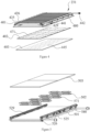
Figure 1 is a stereoscopic view of a wafer optical processing device; -
Figure 2A is a stereoscopic view of the front part and rear part of the wafer optical processing device inFigure 1 with the housing removed; -
Figure 2B is a sectional view of the wafer optical processing device inFigure 2A taken along line A-A; -
Figure 3 is a stereoscopic view of the upper optical processing assembly, the wafer support device, and the lower optical processing assembly; -
Figure 4 is an exploded view of the upper optical processing assembly inFigure 3 ; -
Figure 5 is an exploded view of the lower optical processing assembly inFigure 3 ; and -
Figure 6 is a simplified view of the upper optical processing assembly, the wafer support device, and the lower optical processing assembly inFigure 2B . - Specific embodiments of the present invention will be described below with reference to drawings that constitute part of the Description. It should be understood that although terms for indicating directions, such as "front", "rear", "upper", "lower", "left", and "right", are used herein to describe each demonstrative structural part and component of the present application, use of these terms herein is only intended for convenience of explanation, and these terms are determined on the basis of the demonstrative orientations shown in the drawings. Embodiments disclosed by the present application may be disposed in different directions, and so these terms indicating directions are only illustrative, instead of being construed as limiting.
-
Figure 1 , a stereoscopic view of a wafer optical processing device, is used to explain the external structure of a waferoptical processing device 100. As shown inFigure 1 , the waferoptical processing device 100 is provided with ahousing 101 and a pair ofconveyor passages housing 101 is provided with afront part 111, arear part 112, anupper part 113, alower part 114, aleft part 115, and aright part 116, and thus thehousing 101 roughly forms a box. In the present application, a direction from thefront part 111 to therear part 112 is called a length direction, a direction from theupper part 113 to thelower part 114 is called a height direction, and a direction from theleft part 115 to theright part 116 is called a width direction. Thefront part 111 is provided with awafer inlet 162a, 162b, and therear part 112 is provided with a wafer outlet. Thewafer inlet 162a, 162b and the wafer outlet are in communication with an upstream device and a downstream device, respectively. Theconveyor passages wafer inlet 162a, 162b and the wafer outlet. In other words, theconveyor passages front part 111 and therear part 112 of thehousing 101. In theconveyor passages wafer support devices wafer 150 to be processed. Theupper part 113 of thehousing 101 is provided withair inlets lower part 114 of thehousing 101 is provided withair outlets air inlets air outlets housing 101 through theair inlets air outlets housing 101, an airflow may take away part of the heat in thehousing 101, ensuring that the temperature in thehousing 101 is kept within a preset range. Thelower part 114 of thehousing 101 comprises abase plate 170 andair outlet boxes base plate 170 are respectively connected to thefront part 111, therear part 112, theleft part 115, and theright part 116 of the housing. Thebase plate 170 is provided with an opening; one end of theair outlet boxes base plate 170, and theair outlets air outlet boxes base plate 170 and then flow out through theair outlets -
Figure 2A is a stereoscopic view of the front part and rear part of the wafer optical processing device inFigure 1 with the housing removed, showing the internal components of the wafer optical processing device;Figure 2B is a sectional view ofFigure 2A . InFigure 2A , thefront part 111 and therear part 112 of thehousing 101 are removed, and the internal components of the wafer optical processing device are visible. As shown inFigures 2A and2B , the waferoptical processing device 100 comprises twowafer processing assemblies wafer processing assemblies wafer processing assemblies wafer processing assembly 201a will be described below; the structure of thewafer processing assembly 201b, which is the same as that of thewafer processing assembly 201a, will not be described again. - The
wafer processing assembly 201a comprises anupper plate 213, alower plate 214, aleft plate 215, and a right plate 216; theupper plate 213, thelower plate 214, theleft plate 215, and the right plate 216 form a ring creating acylindrical space 270. Theair inlet 103a is disposed in theupper plate 213, and theair outlet box 172a is connected to thelower plate 214. Aguide rack 281 is disposed below theair inlet 103a; theguide rack 281 extends in the length direction shown inFigure 2A ; the length of theguide rack 281 in the length direction is greater than the diameter of theair inlet 103a and smaller than the length of theupper plate 213 in the length direction. Theguide rack 281 is provided with a base plate 282 andlateral plates Figure 2B ), the upper ends of thelateral plates upper plate 213 of thewafer processing assembly 201a; thus, theguide rack 281 and theupper plate 213 of thewafer processing assembly 201a form a ring creating a guide passage 285, of which both ends are provided with openings, the guide passage 285 guiding the circulation of an airflow in thehousing 101. An airflow that has flowed in through an air inlet 103 flows along the guide passage 285 and flows out through the openings at the front and rear ends of the guide passage 285. In thecylindrical space 270, thewafer support device 140a, the upperoptical processing assembly 231, and the loweroptical processing assembly 232 are disposed. Both sides of the upperoptical processing assembly 231 are respectively connected to theleft plate 215 and the right plate 216 by the corresponding support rack, and the upperoptical processing assembly 231 is located above thewafer support device 140a and separated from thewafer support device 140a by a specific gap. Likewise, both sides of the loweroptical processing assembly 232 are respectively connected to theleft plate 215 and the right plate 216, and the loweroptical processing assembly 232 is located below thewafer support device 140a and separated from thewafer support device 140a by a specific gap. The upperoptical processing assembly 231 and the loweroptical processing assembly 232, respectively, optically process the front face and rear face of thewafer 150 placed on thewafer support device 140a, wherein the front face of thewafer 150 faces the upperoptical processing assembly 231 and the rear face of thewafer 150 faces the loweroptical processing assembly 232. -
Figure 3 is a stereoscopic view of the upperoptical processing assembly 231, thewafer support device 140a, and the loweroptical processing assembly 232; as shown inFigure 3 , thewafer support device 140a comprises aconveyor belt 305 and a pair ofquartz rods 307, theconveyor belt 305 being supported by the pair ofquartz rods 307. Theconveyor belt 305 constitutes a support piece for supporting thewafer 150. Driven by an external force, theconveyor belt 305 moves relative to thequartz rods 307, thereby driving thewafer 150 placed on theconveyor belt 305 to move together, so that thewafer 150 enters the waferoptical processing device 100 through awafer inlet 162a, 162b in thefront part 111 and then leaves the waferoptical processing device 100 through a wafer outlet in therear part 112. Note that the drawings in the present application show only theconveyor belt 305 in the waferoptical processing device 100, but not any conveyor belts outside the waferoptical processing device 100. In the apparatus comprising the waferoptical processing device 100, theconveyor belt 305 penetrates the waferoptical processing device 100 and relevant devices upstream and downstream of the waferoptical processing device 100; in other words, after being processed on theconveyor belt 305 by devices upstream of the waferoptical processing device 100, thewafer 150 enters the waferoptical processing device 100 via theconveyor belt 305; when moving through the waferoptical processing device 100, thewafer 150 is first optically processed by the upperoptical processing assembly 231 and the loweroptical processing assembly 232 and then is conveyed by theconveyor belt 305 to the downstream device in order to be processed in the next procedure. - The upper
optical processing assembly 231 and the loweroptical processing assembly 232 may each produce light having a certain intensity, thereby, respectively, optically processing the front face and rear face of thewafer 150 to accelerate the process of light attenuation. Theconveyor belt 305 is a meshed structure having a hollowed-out portion, and thus light from the loweroptical processing assembly 232 may penetrate the hollowed-out portion on theconveyor belt 305 to optically process the rear face of thewafer 150. -
Figure 4 is an exploded view of the upperoptical processing assembly 231 inFigure 3 ; as shown inFigure 4 , the upperoptical processing assembly 231 comprises anupper cooling device 401, an upperlight source device 402, and an uppertransparent baffle plate 403. Theupper cooling device 401, the upperlight source device 402, and the uppertransparent baffle plate 403 are fixed together by asupport rack 480. The upperlight source device 402 is used to provide a light source for illuminating the front face (namely, the upper surface) of thewafer 150, theupper cooling device 401 is used to absorb the heat generated by the upperlight source device 402, and the uppertransparent baffle plate 403 is used to block foreign substances in theconveyor passage 130a, so that they are not prone to adhere to the upperlight source device 402. The upperlight source device 402 comprises alight source plate 471 that is integrated with a plurality of LED light sources, wherein thelight source plate 471 is dividable into a plurality of LED light source modules, and some or all of the LED light source modules may be started as needed in actual application. When operating, the upperlight source device 402 generates intense heat; in order to keep the temperature in thewafer processing assembly 201a within a suitable range, theupper cooling device 401 is used to absorb part of the heat generated by the upperlight source device 402. The upper cooling device comprises acooling plate 425 and acoil pipe 426 that are made of a metallic material. Thecooling plate 425 is roughly platelike and has a certain thickness, thelower surface 429 of thecooling plate 425 is roughly a smooth plane, and thelight source plate 471 is connected to the lower surface of thecooling plate 425. Thecooling plate 425 is provided with a plurality of grooves formed by being dented inwards from the upper surface, the grooves having a shape that matches the shape of thecoil pipe 426 and being used to accommodate thecoil pipe 426. Thecoil pipe 426 is embedded in thecooling plate 425, and the area of contact between thecoil pipe 426 and thecooling plate 425 is made as large as possible. Thecoil pipe 426 is provided with aninlet 441 and anoutlet 442, and cooling water flows into the coil pipe through theinlet 441 and then flows out through theoutlet 442. Heat generated by the upperlight source device 402, through thecooling plate 425 and thecoil pipe 426, is conveyed to the interior of thecoil pipe 426 and subjected to heat exchange with the cooling water in thecoil pipe 426, so that the cooling water absorbs heat and its temperature increases; finally, the cooling water flows out through theoutlet 442, taking away part of the heat. The uppertransparent baffle plate 403 is disposed below the upperlight source device 402, a plurality ofholes 445 are disposed in the uppertransparent baffle plate 403, and theholes 445 facilitate the circulation of an airflow in a vertical direction around the upper optical processing assembly 431, thus preventing partial overheating near the upperlight source device 402. The uppertransparent baffle plate 403 is made of glass or another transparent material, capable of preventing, to a certain extent, foreign substances from coming into contact with the upperlight source device 402. When a certain amount of foreign substances have accumulated, the uppertransparent baffle plate 403 may be wiped and cleaned. -
Figure 5 is an exploded view of the loweroptical processing assembly 232 inFigure 3 ; similar to the upperoptical processing assembly 231 shown inFigure 4 , the loweroptical processing assembly 232 comprises alower cooling device 501, a lowerlight source device 502, and a lowertransparent baffle plate 503. Thelower cooling device 501, the lowerlight source device 502, and the lowertransparent baffle plate 503 are fixed together by thesupport rack 580. The lowerlight source device 502 is used to provide a light source for illuminating the rear face of thewafer 150, thelower cooling device 501 is used to absorb the heat generated by the lowerlight source device 502, and the lowertransparent baffle plate 503 is used to prevent foreign substances in theconveyor passage 130a from adhering to the lowerlight source device 502. The lowerlight source device 502 is formed by a plurality oflight source modules 571, wherein thelight source modules 571 are LED light source modules, and some or all of the LEDlight source modules 571 may be started as needed in actual application. The plurality oflight source modules 571 may be independent of one another and connected to thelower cooling device 501, respectively. The power of the lowerlight source device 502 and that of the upperlight source device 402 may be set to be the same or different, as determined by the processing requirements for the front face and rear face of thewafer 150. In the present application, the optical processing requirement for the front face of thewafer 150 is greater than the optical processing requirement for the rear face of thewafer 150, because the maximum light energy that the upperlight source device 402 is capable of providing per unit of time is greater than the maximum light energy that the lowerlight source device 502 is capable of providing per unit of time. In the present application, a plurality of separate detachable light source modules are used as the lowerlight source device 502, and an integrated light source module is used as thelower cooling device 501. In another embodiment, a light source module in another form may also be used as needed. The structure of thelower cooling device 501 is the same as the structure of theupper cooling device 401, but thelower cooling device 501 is placed in a direction different from the upper cooling device; theupper surface 529 of thelower cooling device 501 forms a roughly smooth plane, and thecoil pipe 526 is mounted into the grooves of thecooling plate 525 from below thecooling plate 525 and thus located in thecooling plate 525. In other words, thelower cooling device 501 and theupper cooling device 401 are disposed facing each other. Thelight source modules 571 of the loweroptical processing assembly 232 are connected to theupper surface 529 of thecooling plate 525. Heat generated by the lowerlight source device 502, through thecooling plate 525 and thecoil pipe 526, is conveyed to the interior of thecoil pipe 526 and subjected to heat exchange with the cooling water in thecoil pipe 526, so that the cooling water takes away part of the heat. The lowertransparent baffle plate 503 is disposed above the lowerlight source device 502; different from the uppertransparent baffle plate 403, the lowertransparent baffle plate 503 is provided with no holes; the reason is that, because of the action of gravity and the roughly top-down circulation of an airflow in thehousing 101, foreign substances are relatively more prone to be deposited and accumulate on the lowertransparent baffle plate 503. The lowertransparent baffle plate 503, provided with no holes, is capable of preventing foreign substances from falling on the lowerlight source device 502 through a hole. The lowertransparent baffle plate 503 is made of glass or another transparent material. When a certain amount of foreign substances have accumulated, the lowertransparent baffle plate 503 may be wiped and cleaned. In the present application, heat generated by the lowerlight source device 502 is generally lesser than the heat generated by the upperlight source device 402; thus, though the lowertransparent baffle plate 503 is provided with no holes, no partial overheating occurs near the lowerlight source device 502. -
Figure 6 is a simplified view of the upperoptical processing assembly 231, thewafer support device 140a, and the loweroptical processing assembly 232 inFigure 2B , showing more clearly the relative position relationship among the above-mentioned components. As shown inFigure 6 , the upperlight source device 402 of the upperoptical processing assembly 231 is pressed close to the lower surface of theupper cooling device 401, so that theupper cooling device 401 may effectively absorb the heat generated by the upperlight source device 402. "Pressed close" mentioned herein means being close in distance, but there may also be a specific gap between the upperlight source device 402 and theupper cooling device 401. There is aspecific gap 601 between the uppertransparent baffle plate 403 and the upperlight source device 402; thus, in the length direction of the waferoptical processing device 100, anopening 351 is formed between the uppertransparent baffle plate 403 and the upper light source device 402 (seeFigure 3 ). Thegap 601 allows an airflow to flow between the uppertransparent baffle plate 403 and the upperlight source device 402; then, the airflow flows out through theopening 351, thereby taking away part of the heat and preventing partial overheating of the upperlight source device 402. In addition, a plurality ofholes 445 are disposed in the uppertransparent baffle plate 403, the plurality ofholes 445 further facilitating the circulation of an airflow so that the airflow may further flow out penetrating theholes 445 from top to bottom. - Similarly, the lower
optical processing assembly 232 comprises thelower cooling device 501, the lowerlight source device 502, and the lowertransparent baffle plate 503, wherein the lowerlight source device 502 is pressed close to the lower surface of thelower cooling device 501, so that thecooling device 501 may effectively absorb the heat generated by the lowerlight source device 502. "Pressed close" mentioned herein means being close in distance, but there may also be a specific gap between the lowerlight source device 502 and thelower cooling device 501. There is aspecific gap 602 between the lowertransparent baffle plate 503 and the lowerlight source device 502; thus, in the length direction of the waferoptical processing device 100, anopening 352 is formed between the lowertransparent baffle plate 503 and the lower light source device 502 (seeFigure 3 ). Thegap 602 allows an airflow to flow between the lowertransparent baffle plate 503 and the lowerlight source device 502; then, the airflow flows out through theopening 352, thereby taking away part of the heat and preventing partial overheating of the lowerlight source device 502. As described above, the lowertransparent baffle plate 503 is provided with no holes, in order to prevent foreign substances from falling on the lowerlight source device 502 through a hole. - Still referring to
Figure 6 , thewafer support device 140a comprises theconveyor belt 305 and thequartz rods 307. The twoquartz rods 307 are respectively located on either side of theconveyor belt 305. Theconveyor belt 305 is provided with anupper surface 605 and alower surface 607, thelower surface 607 being roughly a plane and coming into contact with the twoquartz rods 307, and thus the twoquartz rods 307 support theconveyor belt 305. In the present application, theconveyor belt 305 forms a support piece for supporting thewafer 150. Aseparation piece 618 is disposed on theupper surface 605 of theconveyor belt 305, and two raisedribs conveyor belt 305 on theseparation piece 618. An inclined plane extending outwards and upwards is formed on the insides of the two raisedribs bottom sides bottom sides wafer 150. Thus, when thewafer 150 is located on theconveyor belt 305, two sides of thewafer 150 in the width direction come into contact with the inclined surfaces or with the tops of the raisedribs wafer 150 and the upper surface of theconveyor belt 305, so that the lower surface of thewafer 150 does not come into contact with the conveyor belt, which is conducive to the formation of a smooth lower surface (namely, the rear face of the wafer) on thewafer 150. In the present application, theconveyor belt 305 is a meshed structure; in other words, theconveyor belt 305 is provided with a hollowed-out portion that penetrates the upper surface and lower surface of theconveyor belt 305. Therefore, light from the lowerlight source device 502 may penetrate the hollowed-out portion and illuminate the lower surface of thewafer 150. In addition, themeshed conveyor belt 305 having a hollowed-out portion facilitates the circulation of airflows on both sides of theconveyor belt 305. Theseparation piece 618 may be integrated with themeshed conveyor belt 305, for example, being formed by folding upwards a plurality of metallic wires that form the upper part of the meshed conveyor belt, or may be a separately formed component that is connected to the upper surface of theconveyor belt 305. - In the present application, the wafer
optical processing device 100 is disposed downstream of a wafer sintering processing device of a sintering furnace, and a wafer, after undergoing the sintering procedure and cooling quickly, is conveyed by theconveyor belt 305 to a wafer inlet of the waferoptical processing device 100. When thewafer 150 is conveyed by theconveyor belt 305 to pass through the waferoptical processing device 100, the upperlight source device 402 and the lowerlight source device 502 of the waferoptical processing device 100 optically process the front face and rear face of thewafer 150, respectively. In this process, the upperlight source device 402 and the lowerlight source device 502 generate intense heat; in order to keep the temperature in the waferoptical processing device 100 within a specific range (for example, 250°C to 300°C), cooling water flowing in theupper cooling device 401 and in thelower cooling device 501 may take way part of the heat; in addition, a fan connected to the waferoptical processing device 100 causes an airflow to flow from theair inlet 103a to theair outlet 104a, thus also taking away part of the heat. A fan may adjust its blast volume based on the temperature in the waferoptical processing device 100, increasing its blast volume when the temperature becomes higher and decreasing its blast volume when the temperature becomes lower. When the wafer reaches a wafer outlet of the waferoptical processing device 100, the optical processing has been completed, and thewafer 150 will be conveyed by the conveyor belt to the next procedure. The optical processing takes only 10 seconds to 30 seconds. In the present application, the waferoptical processing device 100 is capable of processing the front face and rear face of a wafer at the same time, thus increasing the processing efficiency greatly. A wafer of which the front face and rear face are thus processed is applicable to an electrode of a solar cell; the front face and rear face of such an electrode may both receive solar energy.
Claims (9)
- A wafer optical processing device, for optically processing a sintered wafer, comprising:wafer support devices (140a, 140b), said wafer support devices (140a, 140b) comprising a support piece, said support piece being provided with an upper surface (605) and a lower surface (607) that are disposed facing each other, said support piece being hollowed out in a direction from the upper surface (605) to the lower surface (607), said support piece being configured to be capable of supporting said wafer above said upper surface (605);an upper light source device (402), said upper light source device (402) being disposed above said wafer support devices (140a, 140b) and configured to provide a light source that illuminates the upper surface of said support piece (305); anda lower light source device (502), said lower light source device (502) being disposed below said wafer support devices (140a, 140b) and configured to provide a light source that illuminates the lower surface (607) of said support piece (305),wherein said wafer optical processing assembly further comprises:an upper transparent baffle plate (403), said upper transparent baffle plate (403) being located between said upper light source device (402) and said wafer support devices (140a, 140b) and separated from said upper light source device (402), a plurality of holes being disposed in said upper transparent baffle plate (403);and a lower transparent baffle plate (503), said lower transparent baffle plate (503) being located between said lower light source device (502) and said wafer support devices (140a, 140b) and separated from said lower light source device (502), characterised in that the lower transparent baffle plate 503 is provided with no holes.
- The wafer optical processing device as claimed in claim 1, characterized in that
said wafer support device comprises a conveyor belt (305), said conveyor belt (305) forming said support piece. - The wafer optical processing device as claimed in claim 2, characterized in that
a separation piece (618) is disposed on said conveyor belt (305), said separation piece (618) being configured to be capable of separating said wafer and the upper surface of said conveyor belt (305) by a specific gap. - The wafer optical processing device as claimed in claim 1, characterized in that
said upper light source device (402) and said lower light source device (502) respectively comprise a plurality of light source modules, and one or more of said plurality of light source modules may be started when a wafer is optically processed. - The wafer optical processing device as claimed in claim 4, characterized in that
said light source module provides an LED light source. - The wafer optical processing device as claimed in claim 1, characterized in that
the maximum light energy that said upper light source device (402) is capable of providing per unit of time is greater than the maximum light energy that said lower light source device (502) is capable of providing per unit of time. - The wafer optical processing device as claimed in claim 1, characterized in that said wafer optical processing assembly further comprises:an upper cooling device (401), said upper cooling device (401) being disposed above said upper light source device (402) to cool said upper light source device (402),and a lower cooling device (501), said lower cooling device (501) being disposed below said lower light source device (502) to cool said lower light source device (502).
- The wafer optical processing device as claimed in claim 1, characterized in that said wafer optical processing assembly further comprises:
a housing (101), said upper light source device (402) and said lower light source device (502) being both located in said housing (101), said housing comprising air inlets (103a, 103b) and air outlets (104a, 104b), said air inlets (103a, 103b) being located above said housing (101), said air outlets (104a, 140b) being located below said housing, so that an airflow may flow in through said air inlets (103a, 103b) and flow out through said air outlets (104a, 140b). - A sintering furnace, characterized by comprising:a wafer sintering processing device; andthe wafer optical processing device as claimed in any one of claims 1 to 8, said wafer optical processing device being disposed downstream of said wafer sintering processing device.
Applications Claiming Priority (3)
| Application Number | Priority Date | Filing Date | Title |
|---|---|---|---|
| CN201910768522.9A CN112420870B (en) | 2019-08-20 | 2019-08-20 | Wafer light processing device and sintering furnace |
| CN201921357209.8U CN210379090U (en) | 2019-08-20 | 2019-08-20 | Wafer optical processing device and sintering furnace |
| PCT/US2020/046819 WO2021034840A1 (en) | 2019-08-20 | 2020-08-18 | Wafer optical processing device and sintering furnace |
Publications (2)
| Publication Number | Publication Date |
|---|---|
| EP4018487A1 EP4018487A1 (en) | 2022-06-29 |
| EP4018487B1 true EP4018487B1 (en) | 2024-11-27 |
Family
ID=72340408
Family Applications (1)
| Application Number | Title | Priority Date | Filing Date |
|---|---|---|---|
| EP20765395.7A Active EP4018487B1 (en) | 2019-08-20 | 2020-08-18 | Wafer optical processing device and sintering furnace |
Country Status (4)
| Country | Link |
|---|---|
| US (1) | US12381098B2 (en) |
| EP (1) | EP4018487B1 (en) |
| TW (1) | TW202121498A (en) |
| WO (1) | WO2021034840A1 (en) |
Families Citing this family (1)
| Publication number | Priority date | Publication date | Assignee | Title |
|---|---|---|---|---|
| US11798799B2 (en) * | 2021-08-09 | 2023-10-24 | Applied Materials, Inc. | Ultraviolet and ozone clean system |
Citations (1)
| Publication number | Priority date | Publication date | Assignee | Title |
|---|---|---|---|---|
| CN112420870A (en) * | 2019-08-20 | 2021-02-26 | 伊利诺斯工具制品有限公司 | Wafer optical processing device and sintering furnace |
Family Cites Families (8)
| Publication number | Priority date | Publication date | Assignee | Title |
|---|---|---|---|---|
| US8828776B2 (en) * | 2009-04-16 | 2014-09-09 | Tp Solar, Inc. | Diffusion furnaces employing ultra low mass transport systems and methods of wafer rapid diffusion processing |
| US20120181265A1 (en) * | 2010-07-15 | 2012-07-19 | Despatch Industries Limited Partnership | Firing furnace configuration for thermal processing system |
| EP3108508A1 (en) | 2014-02-20 | 2016-12-28 | Applied Materials Italia Srl | Solar cell processing system, conveyor belt system, solar cell production installation and method |
| US9780252B2 (en) * | 2014-10-17 | 2017-10-03 | Tp Solar, Inc. | Method and apparatus for reduction of solar cell LID |
| US20190249923A1 (en) | 2018-02-15 | 2019-08-15 | Illinois Tool Works Inc. | Methods and apparatus to provide closed loop control in a solar cell production system |
| US11538956B2 (en) * | 2018-04-27 | 2022-12-27 | Illinois Tool Works Inc. | Methods and apparatus to control zone temperatures of a solar cell production system |
| WO2019234917A1 (en) * | 2018-06-08 | 2019-12-12 | 東芝三菱電機産業システム株式会社 | Film formation device |
| CN210379090U (en) | 2019-08-20 | 2020-04-21 | 伊利诺斯工具制品有限公司 | Wafer optical processing device and sintering furnace |
-
2020
- 2020-08-05 TW TW109126431A patent/TW202121498A/en unknown
- 2020-08-18 EP EP20765395.7A patent/EP4018487B1/en active Active
- 2020-08-18 US US17/636,266 patent/US12381098B2/en active Active
- 2020-08-18 WO PCT/US2020/046819 patent/WO2021034840A1/en not_active Ceased
Patent Citations (1)
| Publication number | Priority date | Publication date | Assignee | Title |
|---|---|---|---|---|
| CN112420870A (en) * | 2019-08-20 | 2021-02-26 | 伊利诺斯工具制品有限公司 | Wafer optical processing device and sintering furnace |
Also Published As
| Publication number | Publication date |
|---|---|
| US20220277970A1 (en) | 2022-09-01 |
| US12381098B2 (en) | 2025-08-05 |
| WO2021034840A1 (en) | 2021-02-25 |
| TW202121498A (en) | 2021-06-01 |
| EP4018487A1 (en) | 2022-06-29 |
Similar Documents
| Publication | Publication Date | Title |
|---|---|---|
| TWI422717B (en) | Clean bench and method of producing raw material for single crystal silicon | |
| CN101432847B (en) | Byproduct collecting apparatus of semiconductor apparatus | |
| CN103237767B (en) | Solar concentrator | |
| AU2024296468A1 (en) | Recycling system and recycling method for photovoltaic cell module | |
| IT202000024277A1 (en) | PLANT AND APPARATUS METHOD FOR THE RECYCLING OF PHOTOVOLTAIC PANELS | |
| JP2011020147A (en) | Dust collecting/discharging apparatus for laser beam machining | |
| US12381098B2 (en) | Wafer optical processing device and sintering furnace | |
| JP6270912B2 (en) | Die bonding equipment with inert gas atmosphere | |
| CN210379090U (en) | Wafer optical processing device and sintering furnace | |
| WO2025189688A1 (en) | Laser welding device and laser welding apparatus | |
| CN112420870B (en) | Wafer light processing device and sintering furnace | |
| KR102179851B1 (en) | Substrate processing apparatus and in line type substrate processing system using the same | |
| WO2022125325A2 (en) | Sintering equipment | |
| CN115646863A (en) | Direct-suction removing device and sorting system | |
| WO2020159338A1 (en) | Laser head module of laser debonding device | |
| JP2007301442A (en) | Dust removal equipment | |
| JP2012509587A (en) | Silicon substrate for solar cell, manufacturing apparatus and method thereof, and solar cell | |
| KR100996702B1 (en) | Cooling Device and Method of Substrate | |
| CN210586975U (en) | Discharging device of natural gas forging heating furnace | |
| CN101716436A (en) | Filtering method and device thereof used for oil curtain sealing system of graphite processing | |
| CN202058705U (en) | Wafer drying system | |
| JP2006147902A (en) | Method of welding lead | |
| CN210349859U (en) | HIT or HJT process curing and hydrogen passivation integrated machine for solar cell | |
| KR20100048892A (en) | Heat treatment apparatus | |
| CN224205260U (en) | Heating structure |
Legal Events
| Date | Code | Title | Description |
|---|---|---|---|
| STAA | Information on the status of an ep patent application or granted ep patent |
Free format text: STATUS: UNKNOWN |
|
| STAA | Information on the status of an ep patent application or granted ep patent |
Free format text: STATUS: THE INTERNATIONAL PUBLICATION HAS BEEN MADE |
|
| PUAI | Public reference made under article 153(3) epc to a published international application that has entered the european phase |
Free format text: ORIGINAL CODE: 0009012 |
|
| STAA | Information on the status of an ep patent application or granted ep patent |
Free format text: STATUS: REQUEST FOR EXAMINATION WAS MADE |
|
| 17P | Request for examination filed |
Effective date: 20220211 |
|
| AK | Designated contracting states |
Kind code of ref document: A1 Designated state(s): AL AT BE BG CH CY CZ DE DK EE ES FI FR GB GR HR HU IE IS IT LI LT LU LV MC MK MT NL NO PL PT RO RS SE SI SK SM TR |
|
| DAV | Request for validation of the european patent (deleted) | ||
| DAX | Request for extension of the european patent (deleted) | ||
| GRAP | Despatch of communication of intention to grant a patent |
Free format text: ORIGINAL CODE: EPIDOSNIGR1 |
|
| STAA | Information on the status of an ep patent application or granted ep patent |
Free format text: STATUS: GRANT OF PATENT IS INTENDED |
|
| RIC1 | Information provided on ipc code assigned before grant |
Ipc: H01L 21/677 20060101ALI20240619BHEP Ipc: H01L 21/67 20060101ALI20240619BHEP Ipc: H01L 31/20 20060101ALI20240619BHEP Ipc: H01L 31/18 20060101AFI20240619BHEP |
|
| INTG | Intention to grant announced |
Effective date: 20240718 |
|
| GRAS | Grant fee paid |
Free format text: ORIGINAL CODE: EPIDOSNIGR3 |
|
| P01 | Opt-out of the competence of the unified patent court (upc) registered |
Free format text: CASE NUMBER: APP_51627/2024 Effective date: 20240912 |
|
| GRAA | (expected) grant |
Free format text: ORIGINAL CODE: 0009210 |
|
| STAA | Information on the status of an ep patent application or granted ep patent |
Free format text: STATUS: THE PATENT HAS BEEN GRANTED |
|
| REG | Reference to a national code |
Ref country code: DE Ref legal event code: R079 Ref document number: 602020042090 Country of ref document: DE Free format text: PREVIOUS MAIN CLASS: H01L0031180000 Ipc: H10F0071000000 |
|
| AK | Designated contracting states |
Kind code of ref document: B1 Designated state(s): AL AT BE BG CH CY CZ DE DK EE ES FI FR GB GR HR HU IE IS IT LI LT LU LV MC MK MT NL NO PL PT RO RS SE SI SK SM TR |
|
| REG | Reference to a national code |
Ref country code: GB Ref legal event code: FG4D |
|
| REG | Reference to a national code |
Ref country code: CH Ref legal event code: EP |
|
| REG | Reference to a national code |
Ref country code: DE Ref legal event code: R096 Ref document number: 602020042090 Country of ref document: DE |
|
| REG | Reference to a national code |
Ref country code: IE Ref legal event code: FG4D |
|
| REG | Reference to a national code |
Ref country code: LT Ref legal event code: MG9D |
|
| REG | Reference to a national code |
Ref country code: NL Ref legal event code: MP Effective date: 20241127 |
|
| PG25 | Lapsed in a contracting state [announced via postgrant information from national office to epo] |
Ref country code: PT Free format text: LAPSE BECAUSE OF FAILURE TO SUBMIT A TRANSLATION OF THE DESCRIPTION OR TO PAY THE FEE WITHIN THE PRESCRIBED TIME-LIMIT Effective date: 20250327 Ref country code: IS Free format text: LAPSE BECAUSE OF FAILURE TO SUBMIT A TRANSLATION OF THE DESCRIPTION OR TO PAY THE FEE WITHIN THE PRESCRIBED TIME-LIMIT Effective date: 20250327 Ref country code: HR Free format text: LAPSE BECAUSE OF FAILURE TO SUBMIT A TRANSLATION OF THE DESCRIPTION OR TO PAY THE FEE WITHIN THE PRESCRIBED TIME-LIMIT Effective date: 20241127 |
|
| PG25 | Lapsed in a contracting state [announced via postgrant information from national office to epo] |
Ref country code: NL Free format text: LAPSE BECAUSE OF FAILURE TO SUBMIT A TRANSLATION OF THE DESCRIPTION OR TO PAY THE FEE WITHIN THE PRESCRIBED TIME-LIMIT Effective date: 20241127 Ref country code: FI Free format text: LAPSE BECAUSE OF FAILURE TO SUBMIT A TRANSLATION OF THE DESCRIPTION OR TO PAY THE FEE WITHIN THE PRESCRIBED TIME-LIMIT Effective date: 20241127 |
|
| REG | Reference to a national code |
Ref country code: AT Ref legal event code: MK05 Ref document number: 1746603 Country of ref document: AT Kind code of ref document: T Effective date: 20241127 |
|
| PG25 | Lapsed in a contracting state [announced via postgrant information from national office to epo] |
Ref country code: BG Free format text: LAPSE BECAUSE OF FAILURE TO SUBMIT A TRANSLATION OF THE DESCRIPTION OR TO PAY THE FEE WITHIN THE PRESCRIBED TIME-LIMIT Effective date: 20241127 |
|
| PG25 | Lapsed in a contracting state [announced via postgrant information from national office to epo] |
Ref country code: ES Free format text: LAPSE BECAUSE OF FAILURE TO SUBMIT A TRANSLATION OF THE DESCRIPTION OR TO PAY THE FEE WITHIN THE PRESCRIBED TIME-LIMIT Effective date: 20241127 |
|
| PG25 | Lapsed in a contracting state [announced via postgrant information from national office to epo] |
Ref country code: NO Free format text: LAPSE BECAUSE OF FAILURE TO SUBMIT A TRANSLATION OF THE DESCRIPTION OR TO PAY THE FEE WITHIN THE PRESCRIBED TIME-LIMIT Effective date: 20250227 |
|
| PG25 | Lapsed in a contracting state [announced via postgrant information from national office to epo] |
Ref country code: GR Free format text: LAPSE BECAUSE OF FAILURE TO SUBMIT A TRANSLATION OF THE DESCRIPTION OR TO PAY THE FEE WITHIN THE PRESCRIBED TIME-LIMIT Effective date: 20250228 Ref country code: AT Free format text: LAPSE BECAUSE OF FAILURE TO SUBMIT A TRANSLATION OF THE DESCRIPTION OR TO PAY THE FEE WITHIN THE PRESCRIBED TIME-LIMIT Effective date: 20241127 Ref country code: LV Free format text: LAPSE BECAUSE OF FAILURE TO SUBMIT A TRANSLATION OF THE DESCRIPTION OR TO PAY THE FEE WITHIN THE PRESCRIBED TIME-LIMIT Effective date: 20241127 |
|
| PG25 | Lapsed in a contracting state [announced via postgrant information from national office to epo] |
Ref country code: PL Free format text: LAPSE BECAUSE OF FAILURE TO SUBMIT A TRANSLATION OF THE DESCRIPTION OR TO PAY THE FEE WITHIN THE PRESCRIBED TIME-LIMIT Effective date: 20241127 |
|
| PG25 | Lapsed in a contracting state [announced via postgrant information from national office to epo] |
Ref country code: RS Free format text: LAPSE BECAUSE OF FAILURE TO SUBMIT A TRANSLATION OF THE DESCRIPTION OR TO PAY THE FEE WITHIN THE PRESCRIBED TIME-LIMIT Effective date: 20250227 |
|
| PG25 | Lapsed in a contracting state [announced via postgrant information from national office to epo] |
Ref country code: SM Free format text: LAPSE BECAUSE OF FAILURE TO SUBMIT A TRANSLATION OF THE DESCRIPTION OR TO PAY THE FEE WITHIN THE PRESCRIBED TIME-LIMIT Effective date: 20241127 |
|
| PG25 | Lapsed in a contracting state [announced via postgrant information from national office to epo] |
Ref country code: DK Free format text: LAPSE BECAUSE OF FAILURE TO SUBMIT A TRANSLATION OF THE DESCRIPTION OR TO PAY THE FEE WITHIN THE PRESCRIBED TIME-LIMIT Effective date: 20241127 |
|
| PG25 | Lapsed in a contracting state [announced via postgrant information from national office to epo] |
Ref country code: EE Free format text: LAPSE BECAUSE OF FAILURE TO SUBMIT A TRANSLATION OF THE DESCRIPTION OR TO PAY THE FEE WITHIN THE PRESCRIBED TIME-LIMIT Effective date: 20241127 |
|
| PG25 | Lapsed in a contracting state [announced via postgrant information from national office to epo] |
Ref country code: RO Free format text: LAPSE BECAUSE OF FAILURE TO SUBMIT A TRANSLATION OF THE DESCRIPTION OR TO PAY THE FEE WITHIN THE PRESCRIBED TIME-LIMIT Effective date: 20241127 |
|
| PG25 | Lapsed in a contracting state [announced via postgrant information from national office to epo] |
Ref country code: SK Free format text: LAPSE BECAUSE OF FAILURE TO SUBMIT A TRANSLATION OF THE DESCRIPTION OR TO PAY THE FEE WITHIN THE PRESCRIBED TIME-LIMIT Effective date: 20241127 |
|
| PG25 | Lapsed in a contracting state [announced via postgrant information from national office to epo] |
Ref country code: CZ Free format text: LAPSE BECAUSE OF FAILURE TO SUBMIT A TRANSLATION OF THE DESCRIPTION OR TO PAY THE FEE WITHIN THE PRESCRIBED TIME-LIMIT Effective date: 20241127 |
|
| PG25 | Lapsed in a contracting state [announced via postgrant information from national office to epo] |
Ref country code: IT Free format text: LAPSE BECAUSE OF FAILURE TO SUBMIT A TRANSLATION OF THE DESCRIPTION OR TO PAY THE FEE WITHIN THE PRESCRIBED TIME-LIMIT Effective date: 20241127 |
|
| REG | Reference to a national code |
Ref country code: DE Ref legal event code: R097 Ref document number: 602020042090 Country of ref document: DE |
|
| PG25 | Lapsed in a contracting state [announced via postgrant information from national office to epo] |
Ref country code: SE Free format text: LAPSE BECAUSE OF FAILURE TO SUBMIT A TRANSLATION OF THE DESCRIPTION OR TO PAY THE FEE WITHIN THE PRESCRIBED TIME-LIMIT Effective date: 20241127 |
|
| PLBE | No opposition filed within time limit |
Free format text: ORIGINAL CODE: 0009261 |
|
| STAA | Information on the status of an ep patent application or granted ep patent |
Free format text: STATUS: NO OPPOSITION FILED WITHIN TIME LIMIT |
|
| REG | Reference to a national code |
Ref country code: CH Ref legal event code: L10 Free format text: ST27 STATUS EVENT CODE: U-0-0-L10-L00 (AS PROVIDED BY THE NATIONAL OFFICE) Effective date: 20251008 |
|
| PGFP | Annual fee paid to national office [announced via postgrant information from national office to epo] |
Ref country code: DE Payment date: 20250827 Year of fee payment: 6 |
|
| PGFP | Annual fee paid to national office [announced via postgrant information from national office to epo] |
Ref country code: FR Payment date: 20250825 Year of fee payment: 6 |
|
| 26N | No opposition filed |
Effective date: 20250828 |
|
| REG | Reference to a national code |
Ref country code: CH Ref legal event code: H13 Free format text: ST27 STATUS EVENT CODE: U-0-0-H10-H13 (AS PROVIDED BY THE NATIONAL OFFICE) Effective date: 20260324 |
|
| PG25 | Lapsed in a contracting state [announced via postgrant information from national office to epo] |
Ref country code: MC Free format text: LAPSE BECAUSE OF FAILURE TO SUBMIT A TRANSLATION OF THE DESCRIPTION OR TO PAY THE FEE WITHIN THE PRESCRIBED TIME-LIMIT Effective date: 20241127 |
|
| PG25 | Lapsed in a contracting state [announced via postgrant information from national office to epo] |
Ref country code: LU Free format text: LAPSE BECAUSE OF NON-PAYMENT OF DUE FEES Effective date: 20250818 |
|
| PG25 | Lapsed in a contracting state [announced via postgrant information from national office to epo] |
Ref country code: CH Free format text: LAPSE BECAUSE OF NON-PAYMENT OF DUE FEES Effective date: 20250831 |
|
| GBPC | Gb: european patent ceased through non-payment of renewal fee |
Effective date: 20250818 |