EP4016752A1 - Elastic piece assembly and electronic device having elastic piece assembly - Google Patents
Elastic piece assembly and electronic device having elastic piece assembly Download PDFInfo
- Publication number
- EP4016752A1 EP4016752A1 EP20894296.1A EP20894296A EP4016752A1 EP 4016752 A1 EP4016752 A1 EP 4016752A1 EP 20894296 A EP20894296 A EP 20894296A EP 4016752 A1 EP4016752 A1 EP 4016752A1
- Authority
- EP
- European Patent Office
- Prior art keywords
- elastic piece
- electrical contact
- conductive elastic
- conductive
- component
- Prior art date
- Legal status (The legal status is an assumption and is not a legal conclusion. Google has not performed a legal analysis and makes no representation as to the accuracy of the status listed.)
- Granted
Links
Images









Classifications
-
- H—ELECTRICITY
- H01—ELECTRIC ELEMENTS
- H01R—ELECTRICALLY-CONDUCTIVE CONNECTIONS; STRUCTURAL ASSOCIATIONS OF A PLURALITY OF MUTUALLY-INSULATED ELECTRICAL CONNECTING ELEMENTS; COUPLING DEVICES; CURRENT COLLECTORS
- H01R13/00—Details of coupling devices of the kinds covered by groups H01R12/70 or H01R24/00 - H01R33/00
- H01R13/02—Contact members
- H01R13/22—Contacts for co-operating by abutting
- H01R13/24—Contacts for co-operating by abutting resilient; resiliently-mounted
-
- H—ELECTRICITY
- H04—ELECTRIC COMMUNICATION TECHNIQUE
- H04M—TELEPHONIC COMMUNICATION
- H04M1/00—Substation equipment, e.g. for use by subscribers
- H04M1/02—Constructional features of telephone sets
- H04M1/0202—Portable telephone sets, e.g. cordless phones, mobile phones or bar type handsets
- H04M1/026—Details of the structure or mounting of specific components
- H04M1/0264—Details of the structure or mounting of specific components for a camera module assembly
-
- G—PHYSICS
- G03—PHOTOGRAPHY; CINEMATOGRAPHY; ANALOGOUS TECHNIQUES USING WAVES OTHER THAN OPTICAL WAVES; ELECTROGRAPHY; HOLOGRAPHY
- G03B—APPARATUS OR ARRANGEMENTS FOR TAKING PHOTOGRAPHS OR FOR PROJECTING OR VIEWING THEM; APPARATUS OR ARRANGEMENTS EMPLOYING ANALOGOUS TECHNIQUES USING WAVES OTHER THAN OPTICAL WAVES; ACCESSORIES THEREFOR
- G03B17/00—Details of cameras or camera bodies; Accessories therefor
- G03B17/02—Bodies
- G03B17/04—Bodies collapsible, foldable or extensible, e.g. book type
-
- G—PHYSICS
- G03—PHOTOGRAPHY; CINEMATOGRAPHY; ANALOGOUS TECHNIQUES USING WAVES OTHER THAN OPTICAL WAVES; ELECTROGRAPHY; HOLOGRAPHY
- G03B—APPARATUS OR ARRANGEMENTS FOR TAKING PHOTOGRAPHS OR FOR PROJECTING OR VIEWING THEM; APPARATUS OR ARRANGEMENTS EMPLOYING ANALOGOUS TECHNIQUES USING WAVES OTHER THAN OPTICAL WAVES; ACCESSORIES THEREFOR
- G03B17/00—Details of cameras or camera bodies; Accessories therefor
- G03B17/56—Accessories
- G03B17/561—Support related camera accessories
-
- H—ELECTRICITY
- H04—ELECTRIC COMMUNICATION TECHNIQUE
- H04M—TELEPHONIC COMMUNICATION
- H04M1/00—Substation equipment, e.g. for use by subscribers
- H04M1/02—Constructional features of telephone sets
- H04M1/0202—Portable telephone sets, e.g. cordless phones, mobile phones or bar type handsets
-
- H—ELECTRICITY
- H04—ELECTRIC COMMUNICATION TECHNIQUE
- H04M—TELEPHONIC COMMUNICATION
- H04M1/00—Substation equipment, e.g. for use by subscribers
- H04M1/02—Constructional features of telephone sets
- H04M1/0202—Portable telephone sets, e.g. cordless phones, mobile phones or bar type handsets
- H04M1/0206—Portable telephones comprising a plurality of mechanically joined movable body parts, e.g. hinged housings
- H04M1/0208—Portable telephones comprising a plurality of mechanically joined movable body parts, e.g. hinged housings characterized by the relative motions of the body parts
- H04M1/0235—Slidable or telescopic telephones, i.e. with a relative translation movement of the body parts; Telephones using a combination of translation and other relative motions of the body parts
- H04M1/0237—Sliding mechanism with one degree of freedom
-
- H—ELECTRICITY
- H04—ELECTRIC COMMUNICATION TECHNIQUE
- H04N—PICTORIAL COMMUNICATION, e.g. TELEVISION
- H04N23/00—Cameras or camera modules comprising electronic image sensors; Control thereof
- H04N23/50—Constructional details
- H04N23/51—Housings
-
- H—ELECTRICITY
- H04—ELECTRIC COMMUNICATION TECHNIQUE
- H04N—PICTORIAL COMMUNICATION, e.g. TELEVISION
- H04N23/00—Cameras or camera modules comprising electronic image sensors; Control thereof
- H04N23/57—Mechanical or electrical details of cameras or camera modules specially adapted for being embedded in other devices
-
- H—ELECTRICITY
- H01—ELECTRIC ELEMENTS
- H01R—ELECTRICALLY-CONDUCTIVE CONNECTIONS; STRUCTURAL ASSOCIATIONS OF A PLURALITY OF MUTUALLY-INSULATED ELECTRICAL CONNECTING ELEMENTS; COUPLING DEVICES; CURRENT COLLECTORS
- H01R13/00—Details of coupling devices of the kinds covered by groups H01R12/70 or H01R24/00 - H01R33/00
- H01R13/02—Contact members
- H01R13/22—Contacts for co-operating by abutting
- H01R13/24—Contacts for co-operating by abutting resilient; resiliently-mounted
- H01R13/2442—Contacts for co-operating by abutting resilient; resiliently-mounted with a single cantilevered beam
Definitions
- Embodiments of this application relate to the field of electronic devices, and in particular, to an elastic piece assembly and an electronic device with an elastic piece assembly.
- a conductive elastic piece is arranged inside the electronic device, and the components are connected by using the elastic piece.
- the elastic piece can be used to enable connection of electric signals, connection of antennas or grounding connection.
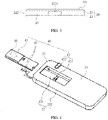
- FIG. 1 is a schematic diagram of a structure in which relatively moving components are electrically connected to each other by using elastic pieces in the prior art.
- the structure includes a first component, a second component and two elastic pieces. One end of each of the elastic pieces is arranged on the first component, and the other end of each of the elastic pieces is a free end and is bent toward the second component.
- Two connecting contacts are arranged on the second component, and the two connecting contacts are located in a direction of relative movement of the first component and the second component.
- a bend apex of the first elastic piece is in contact with the first connecting contact. With relative movement of the first component and the second component, the bend apex of the first elastic piece is out of contact with the first connecting contact until a bend apex of the second elastic piece moves and comes into contact with the second connecting contact.
- Embodiments of this application provide an elastic piece assembly and an electronic device with an elastic piece assembly, so that deformation of each conductive elastic piece can be controlled to ensure that an electrical contact section of the conductive elastic piece has enough elasticity to be in contact with an electrical contact assembly, and the conductive elastic piece is prevented from affecting relative sliding between a first component and a second component.
- an embodiment of this application provides an elastic piece assembly applied to an electronic device, where the electronic device includes a first component and a second component that are capable of sliding relatively in a first direction, and the elastic piece assembly includes a support, an electrical contact assembly, and at least two conductive elastic pieces;
- the conductive elastic pieces each include a fixed end fixedly connected to the support and a connecting end movably connected to the support, and the electrical contact section protrudes toward the electrical contact assembly; and the connecting end is capable of moving relative to the support to limit a protrusion height of the electrical contact section relative to the support.
- the fixed end is fixedly connected to the support, so that the conductive elastic piece can be reliably connected to the support.
- the electrical contact section connected to the fixed end is configured to be in electrical contact with the electrical contact assembly, to connect the conductive elastic piece to the electrical contact assembly.
- the connecting end connected to the electrical contact section moves relative to the support to limit the protrusion height of the electrical contact section relative to the support.
- the support is provided with an accommodating groove, each of the conductive elastic pieces is located in the accommodating groove, and the connecting end is capable of moving in the accommodating groove to limit deformation of the conductive elastic piece.
- the accommodating grooves are provided to accommodate the conductive elastic pieces, so that part or all of the fixed end and the connecting end of each of the conductive elastic pieces is located in the accommodating groove, and a bending point in the electrical contact section can extend out of the accommodating groove.
- the accommodating groove includes a first accommodating part, a guide part and a second accommodating part that communicate with each other in sequence, the fixed end is located in the first accommodating part and connected to the first accommodating part, and the connecting end is located in the second accommodating part.
- the second accommodating part is internally provided with two extended sections extending toward opposite sides of the support respectively, two opposite sides of the connecting end are provided with extended buckles, and the extended buckles are located in the extended sections.
- the extended sections are arranged in the second accommodating part, the connecting end is provided with the extended buckles, and the extended buckles each are located in the extended section and match the extended section, so that the extended buckle can move in the extended section in the first direction to limit deformation of the conductive elastic piece. This enables the support to slide smoothly, and ensures conductive stability of the conductive elastic piece.
- the electrical contact section includes a first inclined part, a first contact part and a second inclined part that are connected in sequence, the first contact part abuts against the electrical contact assembly, and the first inclined part and the second inclined part are inclined toward the electrical contact assembly.
- the first inclined part and the second inclined part are arranged on the electrical contact section to serve as a buffer for the conductive elastic piece in a sliding process, so that the first contact part gradually slides to a position in contact with the electrical contact assembly.
- An included angle between the first inclined part and a plane where the fixed end is located is greater than or equal to 10° and less than or equal to 70°
- an included angle between the second inclined part and a plane where the fixed end is located is greater than or equal to 10° and less than or equal to 70°. Larger included angles indicate a better buffering effect on the conductive elastic piece in the sliding process.
- the first contact part is provided with a plating layer for reducing impedance of the first contact part.
- the elastic piece assembly there are two conductive elastic pieces, the electrical contact sections of the two conductive elastic pieces face opposite directions, the two conductive elastic pieces are parallel to the first direction, and a distance between the electrical contact sections of the two conductive elastic pieces is equal to a sliding distance between the first component and the second component.
- the two conductive elastic pieces are staggered in the first direction, or the two conductive elastic pieces are located on the same straight line.
- the first contact parts of the two conductive elastic pieces are in contact with different positions of the electrical contact assembly, respectively. In this way, wear of the electrical contact assembly and the conductive elastic piece can be prevented, and service lives of the electrical contact assembly and the conductive elastic piece can be prolonged.
- the electrical contact assembly includes a mounting frame and a conductive part connected to the mounting frame, the mounting frame is configured to be connected to the first component, and each of the electrical contact sections abuts against the conductive part.
- At least one side of the conductive part is provided with at least one positioning notch
- the mounting frame is provided with a positioning part matching the positioning notch
- the conductive part is provided with at least one bent part bent toward the mounting frame, and each of the bent parts abuts against an end portion of the mounting frame when the conductive part is connected to the mounting frame.
- the conductive part includes a second contact part and guide edges each connected to an edge of the second contact part, each of the first contact parts abuts against the second contact part, the guide edge is inclined toward the mounting frame, and an extension direction of the guide edge is perpendicular to the first direction.
- the positioning notch and the bent part on the conductive part are located on different sides of the conductive part respectively.
- the guide edges are located on opposite sides of the second contact part respectively, and an included angle between each of the guide edges and the second contact part is 10°-70°. A larger included angle between the guide edge and the second contact part indicates a better buffering effect.
- the positioning notch is located on the guide edge.
- An arc is arranged at an intersection of the second contact part and the guide edge. The arc can also buffer the conductive elastic piece in a relative movement process, which prevents scratching in the sliding process, thereby prolonging the service life of the conductive elastic piece.
- an embodiment of this application further provides an electronic device with an elastic piece assembly, including a first component, a second component and the elastic piece assembly according to the foregoing embodiment, where the first component is connected to the second component by using the elastic piece assembly.
- the first component is a camera assembly and the second component is a middle frame; or the first component is a middle frame and the second component is a camera assembly.
- the first component is a sliding housing and the second component is a fixed housing; or the first component is a fixed housing and the second component is a sliding housing.
- This application provides the elastic piece assembly and the electronic device with an elastic piece assembly.
- the two ends of each of the conductive elastic pieces are connected to the support, so that deformation of the conductive elastic piece is controlled to ensure that the electrical contact section of the conductive elastic piece has enough elasticity to be in contact with the electrical contact assembly, and the conductive elastic piece is prevented from affecting relative sliding between the first component and the second component.
- An embodiment of this application provides an electronic device, including but not limited to a mobile or fixed terminal with a display screen and a housing, such as a mobile phone, a tablet computer, a notebook computer, an ultra-mobile personal computer (ultra-mobile personal computer, UMPC), a netbook, a POS machine, a personal digital assistant (personal digital assistant, PDA), a wearable device and a virtual reality device.
- a mobile or fixed terminal with a display screen and a housing
- a mobile phone a tablet computer, a notebook computer, an ultra-mobile personal computer (ultra-mobile personal computer, UMPC), a netbook, a POS machine, a personal digital assistant (personal digital assistant, PDA), a wearable device and a virtual reality device.
- UMPC ultra-mobile personal computer
- PDA personal digital assistant
- FIG. 1 is a schematic diagram of a structure in which relatively moving components are electrically connected to each other by using elastic pieces in the prior art.
- the structure includes a first component 300, a second component 400 and two elastic pieces 200.
- One end of each of the elastic pieces 200 is arranged on the first component 300, and the other end of each of the elastic pieces 200 is a free end and is bent toward the second component 400.
- Two connecting contacts 500 are arranged on the second component 400, and the two connecting contacts 500 are located in a direction of relative movement of the first component 300 and the second component 400.
- a bend apex of the first elastic piece 200 is in contact with the first connecting contact 500.
- an embodiment of this application provides an electronic device.
- a support 41 in the electronic device is located in an accommodating chamber 23, an electrical contact section 431 on a first conductive elastic piece 43 on the support 41 is in contact with an electrical contact assembly 42.
- a driving assembly drives the support 41 to slide, so that the second component 400 on the support 41 extends out of the accommodating chamber 23 through the through hole 2221.
- the electrical contact section 431 on the first conductive elastic piece 43 is gradually out of contact with the electrical contact assembly 42 until the electrical contact section 431 on the second conductive elastic piece 43 on the support 41 comes into contact with the electrical contact assembly 42, so that the second component 400 is still electrically connected to a battery of a mobile phone 100.
- each of the conductive elastic pieces 43 Two ends of each of the conductive elastic pieces 43 are connected to the support 41, so that deformation of the conductive elastic piece 43 is controlled to ensure that the electrical contact section 431 of the conductive elastic piece 43 has enough elasticity to be in contact with the electrical contact assembly 42, and the conductive elastic piece 43 is prevented from affecting relative sliding between the second component 400 and the first component 300.
- the electronic device according to this application is described in detail by using the following specific embodiments, which can be combined with each other.
- the same or similar contents are not described in different embodiments again.
- the mobile phone 100 is used as an example of the terminal to describe the following embodiments in detail.
- FIG. 2 is a schematic structural diagram of an electronic device according to an embodiment of this application
- FIG. 3 is a side view of an electronic device according to an embodiment of this application.
- the mobile phone 100 may include a display screen 10, a housing 20, and a camera assembly 30.
- the display screen 10 is connected to the housing 20, and the camera assembly 30 is located on the housing 20.
- the display screen 10 may be an organic light-emitting diode (organic light-emitting diode, OLED) display screen or a liquid crystal display (liquid crystal display, LCD). It should be understood that the display screen 10 may include a display and a touch device. The display is configured to output display content to a user, and the touch device is configured to receive a touch event input by the user on the display screen 10.
- OLED organic light-emitting diode
- LCD liquid crystal display
- the housing 20 may include a rear cover 21 and a middle frame 22.
- the middle frame 22 is located between the display screen 10 and the rear cover 21.
- the display screen 10 is connected to one side of the middle frame 22, and the rear cover 21 is connected to the other side of the middle frame 22.
- the display screen 10, the rear cover 21 and the middle frame 22 jointly enclose the accommodating chamber 23.
- the accommodating chamber 23 contains a battery, a circuit board, a communications module (not shown in the figure), and the like.
- a battery compartment may be arranged on one side of the middle frame 22 facing the rear cover 21, and the battery is installed in the battery compartment.
- the battery can be connected to a charging management module and the circuit board by using a power management module, and the power management module receives an input of the battery and/or the charging management module and supplies power to the processor, an internal memory, an external memory, the display screen 10, the camera assembly 30, the communications module, and the like.
- the power management module may be further configured to monitor battery capacity, battery cycle times, battery health statuses (leakage and impedance) and other parameters.
- the power management module may alternatively be disposed in the processor of the circuit board.
- the power management module and the charging management module may alternatively be arranged in the same device.
- the middle frame 22 may include a metal middle plate 221 and a bezel 222.
- One round of bezel 222 is disposed around an edge of the metal middle plate 221.
- the bezel 222 is located between the display screen 10 and the rear cover 21, and the bezel 222 is exposed to the outside.
- the display screen 10, the rear cover 21 and the bezel 222 jointly enclose the accommodating chamber 23, and the middle frame 22 is located in the accommodating chamber 23.
- the material of the metal middle plate 221 may include, but is not limited to, aluminum alloy, stainless steel, a steel-aluminum composite die-casting plate or titanium alloy.
- the bezel 222 may be a metal bezel, or the bezel 222 may alternatively be a non-metal bezel, such as a ceramic bezel or a glass bezel.
- the material of the metal bezel includes, but is not limited to, aluminum alloy, stainless steel or titanium alloy.
- the rear cover 21 may be a metal rear cover, a glass rear cover, a plastic rear cover or a ceramic rear cover. In this embodiment of this application, the material of the rear cover 21 is not limited.
- the first component 300 may be the housing 20 and the second component 400 may be the camera assembly 30.
- the camera assembly 30 may include a front camera and/or a rear camera, a flash, a miniature projection apparatus, and the like. Details are not described herein again.
- the camera assembly 30 may be located in the accommodating chamber 23.
- the front camera is disposed in the accommodating chamber 23, and when in use, by sliding the front camera, the front camera slides relative to the housing 20, so that the front camera extends out of the accommodating chamber 23, so as to perform operations such as photographing or video shooting.
- the front camera is hidden in the accommodating chamber 23, so that a screen-to-body ratio is increased, which makes it easier to obtain a good visual impression in the appearance design of the mobile phone 100.
- the rear camera may alternatively be disposed in the accommodating chamber 23, and when in use, by sliding the rear camera, the rear camera slides relative to the housing 20, so that the rear camera extends out of the accommodating chamber 23, so as to perform operations such as photographing or video shooting.
- FIG. 4 is an exploded view of an electronic device according to an embodiment of this application.
- the mobile phone 100 may further include an elastic piece assembly 40.
- the elastic piece assembly 40 includes a support 41, an electrical contact assembly 42 and at least two conductive elastic pieces 43.
- the electrical contact assembly 42 is connected to the housing 20, and the support 41 is connected to the camera assembly 30.
- each of the conductive elastic pieces 43 Two ends of each of the conductive elastic pieces 43 are connected to the support 41, the conductive elastic piece 43 is provided with an electrical contact section 431 bent toward the electrical contact assembly 42, and the electrical contact section 431 is located between two end portions of the conductive elastic piece 43; the conductive elastic pieces 43 are separately and sequentially arranged in the first direction, and when the housing 20 and the camera assembly 30 slide relatively, the electrical contact assembly 42 abuts against the electrical contact sections of different conductive elastic pieces 43 to connect the electrical contact assembly 42 to the conductive elastic pieces 43.
- the electrical contact assembly 42 is connected to the circuit board in the housing 20, the circuit board is connected to the battery, the circuit board in the housing 20 supplies power to the electrical contact assembly 42, and when the camera assembly 30 and the housing 20 slide relatively, or when the camera assembly 30 and the housing 20 are both in a relatively static state, the electrical contact assembly 42 is kept in a charged state.
- the elastic piece assembly 40 may further include a support 41, and the support 41 supports the camera assembly 30.
- a first connecting part may be disposed on the support 41 and a second connecting part may be disposed on the camera assembly 30, and the first connecting part is connected to the second connecting part through bonding, clamping or screw connection, or the like, so that the camera assembly 30 is installed on the support 41.
- the material of the support 41 may be the same as that of the bezel 222, and the material of the support 41 may alternatively be different from that of the bezel 222. This is not limited in this embodiment.
- the support 41 may be divided into two parts, which are an upper half of the support 41 and a lower half of the support 41.
- the camera assembly 30 is located on the upper half of the support 41, and the upper half of the support 41 can extend out of the accommodating chamber 23 to drive the camera assembly 30 to extend out of the accommodating chamber 23.
- the lower half of the support 41 is configured to be connected to the conductive elastic piece 43, and when the camera assembly 30 slides relative to the housing 20, the lower half of the support 41 is located in the accommodating chamber 23. This prevents a situation that the conductive elastic piece 43 located in the lower half of the support 41 extends out of the accommodating chamber 23 and is corroded by water vapor and the like outside the accommodating chamber 23, thereby affecting conductive performance of the conductive elastic piece 43.
- the camera assembly 30 can be embedded in the upper half of the support 41, so as to avoid increasing the overall thickness of the mobile phone 100, and the camera assembly 30 can be reliably connected in the support 41. Because the camera assembly 30 is disposed in the upper half of the support 41, a thickness of the upper half of the support 41 may be greater than that of the lower half of the support 41.
- a stepped surface 412 is formed due to a thickness difference at a joint between the upper half of the support 41 and the lower part of the support 41. The stepped surface 412 can also be used as a limiting part for the camera assembly 30 to extend out of the accommodating chamber 23. An abutting part may be disposed in the accommodating chamber 23.
- the stepped surface 412 moves to the abutting part of the accommodating chamber 23, the stepped surface 412 abuts against the abutting part, thereby preventing the support 41 from continuing movement. In this case, the camera assembly 30 is completely removed from the accommodating chamber 23.
- the bezel 222 is provided with a through hole 2221 for the support 41 to enter or exit the accommodating chamber 23.
- the support 41 extends out of the accommodating chamber 23 through the through hole 2221, and the support 41 drives the camera assembly 30 to extend out of the accommodating chamber 23 through the through hole 2221.
- the through hole 2221 is located in the bezel 222. That is, the support 41 slides relative to the metal middle plate 221 so that the camera assembly 30 slides relative to the housing 20.
- a driving assembly may be disposed in the accommodating chamber 23, the driving assembly may be disposed on the metal middle plate 221, and the support 41 may be connected to the driving assembly in the accommodating chamber 23.
- the support 41 is driven by the driving assembly to slide to extend out of or enter the accommodating chamber 23.
- the driving assembly may include an electromagnetic telescopic motor.
- a guide rail may further be disposed in the accommodating chamber 23.
- Other driving assemblies may alternatively be used to drive the support 41 to extend out of or enter the accommodating chamber 23. This is not limited in this embodiment.
- an inner sidewall of the through hole 2221 matches an outer sidewall of the support 41.
- the support 41 is at least partially cylindrical, and an outer diameter of the support 41 is equal to an inner diameter of the through hole 2221.
- the support 41 is at least partially a quadrangular prism, and the cross section of the support 41 perpendicular to an axial direction of the support 41 is the same as a plane enclosed by an inner contour of the through hole 2221.
- the conductive elastic pieces 43 are separately and sequentially arranged in the first direction.
- the first direction is a direction of sliding of the support 41 relative to the bezel 222, which is also a direction in which the support 41 slides out of or enters the bezel 222.
- Each of the conductive elastic pieces 43 is connected to the support 41, and each of the conductive elastic pieces 43 is electrically connected to the camera assembly 30.
- the first conductive elastic piece 43 is connected to the front camera in the camera assembly 30, the second conductive elastic piece 43 is connected to the rear camera in the camera assembly 30, the second conductive elastic piece 43 is connected to the front camera in the camera assembly 30, and the third conductive elastic piece 43 is connected to the flash in the camera assembly 30.
- the first conductive elastic piece 43 may be connected to the camera assembly 30 by using a wire, and the conductive elastic piece 43 may be connected to the camera assembly 30 by using a metal sheet. This is not limited in this embodiment.
- the electrical contact section 431 on the first conductive elastic piece 43 on the support 41 is in contact with an electrical contact assembly 42.
- the driving assembly drives the support 41 to slide, so that the camera assembly 30 on the support 41 extends out of the accommodating chamber 23 through the through hole 2221.
- the electrical contact section 431 on the first conductive elastic piece 43 is gradually out of contact with the electrical contact assembly 42 until the electrical contact section 431 on the second conductive elastic piece 43 on the support 41 comes into contact with the electrical contact assembly 42, so that the camera assembly 30 is still electrically connected to the battery of the mobile phone 100, and the camera assembly 30 to perform photographing or video shooting.
- each of the conductive elastic pieces 43 are connected to the support 41, so that deformation of the conductive elastic piece 43 is controlled to ensure that the electrical contact section 431 of the conductive elastic piece 43 has enough elasticity to be in contact with the electrical contact assembly 42, and the conductive elastic piece 43 is prevented from affecting relative sliding between the support 41 and the metal middle plate 221.
- FIG. 5 is a schematic structural diagram of a conductive elastic piece in an electronic device according to an embodiment of this application
- FIG. 6 is a schematic structural diagram of a conductive elastic piece and a support in an electronic device according to an embodiment of this application
- FIG. 7 is a schematic structural diagram of a conductive elastic piece and a support in another direction in an electronic device according to an embodiment of this application.
- the conductive elastic piece 43 includes a fixed end 432 fixedly connected to the support 41 and a connecting end 433 movably connected to the support 41, and the electrical contact section 431 protrudes toward the electrical contact assembly 42.
- the connecting end 433 can move relative to the support 41 to limit the protrusion height of the electrical contact section 431 relative to the support 41.
- the conductive elastic piece 43 may be divided into three sections that are connected in sequence.
- the first section of the conductive elastic piece 43 is the fixed end 432, and the fixed end 432 is fixedly connected to the support 41.
- the second section of the conductive elastic piece 43 is the electrical contact section 431, and the electrical contact section 431 is in electrical contact with the electrical contact assembly 42.
- the third section of the conductive elastic piece 43 is the connecting end 433, and the connecting end 433 is movably connected to the support 41, that is, the connecting end 433 can move relative to the support 41 to limit the protrusion height of the electrical contact section 431 relative to the support 41.
- the fixed end 432, the electrical contact section 431 and the connecting end 433 are connected in sequence.
- the fixed end 432 may be flat to increase a contact surface between the fixed end 432 and the support 41.
- the fixed end 432 may be fixedly connected to the support 41 by using a screw, welding or bonding.
- the electrical contact section 431 may be a bent part of the conductive elastic piece 43, the conductive elastic piece 43 is bent toward the electrical contact section 431, and a bending point in the electrical contact section 431 is in pressure contact with the electrical contact assembly 42.
- the bending point in the electrical contact section 431 may also be called a contact, and the contact is in pressure contact with the electrical contact assembly 42 to connect the conductive elastic piece 43 to the electrical contact assembly 42.
- the connecting end 433 is movably connected to the support 41.
- the connecting end 433 of the conductive elastic piece 43 moves along the support 41 in a direction opposite to a direction in which the conductive elastic piece 43 is compressed, and the conductive elastic piece 43 extends to restore the height of the conductive elastic piece 43 in the extended state, so that the distance between the conductive elastic piece 43 and the electrical contact assembly 42 is maximum.
- the protrusion height of the electrical contact section 431 relative to the support 41 is limited.
- the fixed end 432 is fixedly connected to the support 41, so that the conductive elastic piece 43 can be reliably connected to the support 41.
- the electrical contact section 431 connected to the fixed end 432 is configured to be in electrical contact with the electrical contact assembly 42, to connect the conductive elastic piece 43 to the electrical contact assembly 42.
- the connecting end 433 connected to the electrical contact section 431 moves relative to the support 41 to limit the protrusion height of the electrical contact section 431 relative to the support 41.
- the support 41 is provided with an accommodating groove 411, each of the conductive elastic pieces 43 is located in the accommodating groove 411, and the connecting end 433 is capable of moving in the accommodating groove 411 to limit deformation of the conductive elastic piece 43.
- an extending direction of the accommodating groove 411 may be parallel to the first direction, the conductive elastic pieces 43 are arranged in the accommodating groove 411, and the fixed end 432 of each of the conductive elastic pieces 43 is fixedly connected to the bottom of the accommodating groove 411.
- the connecting end 433 of each of the conductive elastic pieces 43 moves in the accommodating groove 411 to limit deformation of the conductive elastic piece 43.
- the quantity of the accommodating grooves 411 is equal to the quantity of the conductive elastic pieces 43, and one conductive elastic piece 43 is placed in one accommodating groove 411. In this way, it is convenient to install the conductive elastic pieces 43 in the accommodating grooves 411, and the conductive elastic pieces 43 do not affect each other during installation.
- the bending point in the electrical contact section 431 can be in contact with the electrical contact assembly 42 when the accommodating groove 411 accommodates the conductive elastic piece 43. That is, the fixed end 432 and the connecting end 433 of each of the conductive elastic pieces 43 are at least partially located in the accommodating groove 411, and the bending point in the electrical contact section 431 can extend out of the accommodating groove 411 and can be in contact with the electrical contact assembly 42.
- the accommodating grooves 411 are provided to accommodate the conductive elastic pieces 43, so that part or all of the fixed end 432 and the connecting end 433 of each of the conductive elastic pieces 43 is located in the accommodating groove 411, and the bending point in the electrical contact section 431 can extend out of the accommodating groove 411.
- the accommodating grooves 411 are provided to accommodate the conductive elastic pieces 43 and reduce the overall thickness of the mobile phone 100.
- the conductive elastic piece 43 is divided into the fixed end 432, the electrical contact section 431 and the connecting end 433 that are connected in sequence.
- the fixed end 432, the electrical contact section 431 and the connecting end 433 have different functions.
- the accommodating groove 411 for accommodating the conductive elastic piece 43 is divided into different areas. The different areas of the accommodating groove 411 are described below.
- the accommodating groove 411 includes a first accommodating part 4111, a guide part 4112 and a second accommodating part 4113 that communicate with each other in sequence, the fixed end 432 is located in the first accommodating part 4111, the fixed end 432 is connected to the first accommodating part 4111, and the connecting end 433 is located in the second accommodating part 4113.
- the fixed end 432 is configured to be connected to the first accommodating part 4111, so as to reliably connect the fixed end 432 into the first accommodating part 4111.
- a size of the fixed end 432 can be increased in the conductive elastic piece 43 to increase a contact area between the fixed end 432 and the first accommodating part 4111. That is, a width D1 of the fixed end 432 is greater than a width D2 of the connecting end 433, and the width D2 of the connecting end 433 may be equal to a width D3 of the guide part 4112.
- the first accommodating part 4111 matches the fixed end 432, and a size of the first accommodating part 4111 is greater than that of the second accommodating part 4113.
- the fixed end 432 may be fixedly connected to the first accommodating part 4111 by using a screw, welding or bonding.
- the fixed end 432 is electrically connected to the first accommodating part 4111
- the camera assembly 30 is electrically connected to the first accommodating part 4111 in the support 41, so as to electrically connect the conductive elastic piece 43 to the camera assembly 30.
- the connecting end 433 matches the second accommodating part 4113.
- the accommodating groove 411 includes a first accommodating part 4111, a guide part 4112 and a second accommodating part 4113 that communicate with each other in sequence, the fixed end 432 is located in the first accommodating part 4111, and the connecting end 433 is located in the second accommodating part 4113. This facilitates installation of the conductive elastic piece 43 and can prevent reverse installation of the conductive elastic piece 43.
- the second accommodating part 4113 is internally provided with two extended sections 4114 extending toward opposite sides of the support 41 respectively, two opposite sides of the connecting end 433 are provided with extended buckles 4331, and the extended buckles 4331 are located in the extended sections 4114.
- the two extended sections 4114 may be disposed in a width direction of the second accommodating part 4113 (that is, a width D2 direction of the connecting end 433), the two extended sections 4114 extend in the width D2 direction of the connecting end 433, and the two extended sections 4114 extend in opposite directions.
- Two sides of the connecting end 433 are provided with two extended buckles 4331, the extended buckles 4331 extend in the width D2 direction of the connecting end 433, and the two extended buckles 4331 extend in opposite directions.
- the two extended buckles 4331 may be flush with an end portion of the connecting end 433.
- the extended sections 4114 are arranged in the second accommodating part 4113, the connecting end 433 is provided with the extended buckles 4331, and the extended buckles 4331 each are located in the extended section 4114 and match the extended section 4114, so that the extended buckle 4331 can move in the extended section 4114 in the first direction to limit deformation of the conductive elastic piece 43.
- This enables the support 41 to slide smoothly, and ensures conductive stability of the conductive elastic piece 43.
- the electrical contact section 431 includes a first inclined part 4311, a first contact part 4312 and a second inclined part 4313 that are connected in sequence.
- the first contact part 4312 abuts against the electrical contact assembly 42, and the first inclined part 4311 and the second inclined part 4313 are inclined toward the electrical contact assembly 42.
- the electrical contact section 431 may be formed through bending, the bending point of the electrical contact section 431 is the first contact part 4312, the first contact part 4312 is in contact with the electrical contact assembly 42, the first inclined part 4311 may be connected to the fixed end 432, the second inclined part 4313 may be connected to the connecting end 433, and the first inclined part 4311 and the second inclined part 4313 are inclined toward the electrical contact assembly 42.
- the first inclined part 4311 and the second inclined part 4313 are arranged on the electrical contact section 431 to serve as a buffer for the conductive elastic piece 43 in the sliding process, so that the first contact part 4312 gradually slides to a position in contact with the electrical contact assembly 42.
- An angle at which the first inclined part 4311 is inclined toward the electrical contact assembly 42 and an angle at which the second inclined part 4313 is inclined toward the electrical contact assembly 42 may be the same or different. This is not limited in this embodiment.
- an included angle A between the first inclined part 4311 and a plane where the fixed end 432 is located is greater than or equal to 10° and less than or equal to 70°
- an included angle B between the second inclined part 4313 and a plane where the fixed end 432 is located is greater than or equal to 10° and less than or equal to 70°.
- the included angle A between the first inclined part 4311 and the plane where the fixed end 432 is located is an included angle in an anticlockwise direction between the first inclined part 4311 and the plane where the fixed end 432 is located
- the included angle B between the second inclined part 4313 and the plane where the fixed end 432 is located is an included angle in a clockwise direction between the second inclined part 4313 and the plane where the fixed end 432 is located.
- a larger included angle A and included angle B indicate a better buffering effect on the conductive elastic piece 43 in the sliding process.
- a larger included angle A and included angle B also indicate a corresponding increase in the length of the conductive elastic piece 43.
- the first contact part 4312 in the electrical contact section 431 is configured to be in contact with the electrical contact assembly 42.
- the first contact part 4312 is provided with a plating layer for reducing impedance of the first contact part 4312.
- Impedance is the general term for resistance, inductance and capacitance in a circuit that hinder an alternating current.
- a surface of the first contact part 4312 may be electroplated with pure gold or nickel and the like, so as to reduce impedance of the first contact part 4312.
- the surface of the electrical contact section 431 or the surface of the entire conductive elastic piece 43 may alternatively electroplated with pure gold or nickel. This is not limited in this embodiment.
- the electrical contact sections 431 of the two conductive elastic pieces 43 face opposite directions, the two conductive elastic pieces 43 are both parallel to the first direction, and a distance between the electrical contact sections 431 of the two conductive elastic pieces 43 is equal to a sliding distance between the first component 300 and the second component 400.
- the two conductive elastic pieces 43 are located in different accommodating grooves 411 respectively, and the two conductive elastic pieces 43 are parallel to each other.
- the two conductive elastic pieces 43 may face the same direction, that is, the electrical contact sections 431 of the two conductive elastic pieces 43 may both face the through hole 2221.
- the two conductive elastic pieces 43 may alternatively face different directions, that is, the electrical contact sections 431 of the two conductive elastic pieces 43 face opposite directions.
- a relative positional relationship between the two conductive elastic pieces 43 is related to a designed sliding distance of the support 41. Specifically, the distance between the first contact parts 4312 of the two conductive elastic pieces 43 in the first direction is equal to the designed sliding distance of the support 41. That is, the distance between the electrical contact sections 431 of the two conductive elastic pieces 43 is equal to the sliding distance of the camera assembly 30.
- the distance between the electrical contact sections 431 of the two conductive elastic pieces 43 may be adjusted through an arrangement of the two conductive elastic pieces 43.
- a possible arrangement of the two conductive elastic pieces 43 is described with reference to the drawings.
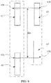
- FIG. 8 is an arrangement diagram of conductive elastic pieces in an electronic device according to an embodiment of this application.
- a distance D4 between the electrical contact sections 431 of the two conductive elastic pieces 43 is fixed, more space of the support 41 is occupied when the two conductive elastic pieces 43 face the same direction compared with when the two conductive elastic pieces 43 face different directions. Therefore, the two conductive elastic pieces 43 are set as facing different directions, which can save the space of the accommodating chamber 23 occupied by the support 41, so that the accommodating chamber 23 of the mobile phone 100 can be used to arrange other parts.
- the distance D4 between the electrical contact sections 431 of the two conductive elastic pieces 43 is relatively large, there is a distance between the two conductive elastic pieces 43 so as to meet requirements for the distance D4.
- the two conductive elastic pieces 43 are located on the same straight line, or the two conductive elastic pieces 43 may be staggered.
- the two conductive elastic pieces 43 need to overlap so as to meet requirements for the distance D4. In this case, the two conductive elastic pieces 43 are staggered in the first direction.
- the first contact parts 4313 of the two conductive elastic pieces 43 are in contact with different positions of the electrical contact assembly 42, respectively. In this way, wear of the electrical contact assembly 42 and the conductive elastic piece 43 can be prevented, and service lives of the electrical contact assembly 42 and the conductive elastic piece 43 can be prolonged.
- FIG. 9 is a schematic internal structural diagram of a housing in an electronic device according to an embodiment of this application
- FIG. 10 is a partial enlarged diagram of a position C in FIG. 9
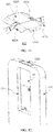
- FIG. 11 is a schematic structural diagram of a conductive part of an electrical contact assembly in an electronic device according to an embodiment of this application.
- the electrical contact assembly 42 includes a mounting frame 421 and a conductive part 422 connected to the mounting frame 421, the mounting frame 421 is configured to be connected to the first component 300, and each of the electrical contact sections 431 abuts against the conductive part 422.
- the mounting frame 421 is connected to the metal middle plate 221.
- the mounting frame 421 may be integrally formed with the metal middle plate 221, or the mounting frame 421 may be welded, bonded, clamped or connected by using a screw to the metal middle plate 221.
- the mounting frame 421 provides an installation space for the conductive part 422 and supports the conductive part 422.
- the conductive part 422 may be welded, bonded, clamped or connected by using a screw to the mounting frame 421, so as to reliably connect the conductive part 422 to the mounting frame 421.
- the conductive part 422 may be a metal sheet.
- At least one side of the conductive part 422 is provided with at least one positioning notch 4221, and the mounting frame 421 is provided with a positioning part 4211 matching the positioning notch 4221.
- the two positioning notches 4221 may be located at two opposite ends of the conductive part 422.
- the first positioning notch 4221 is located at a first end of the conductive part 422, and the second positioning notch 4221 is located at a second end of the conductive part 422.
- the first end of the conductive part 422 is opposite to the second end of the conductive part 422.
- the positioning parts 4211 are located at two opposite ends of the mounting frame 421.
- the positioning parts 4211 each may be a positioning column, and the positioning notches 4221 are clamped on different positioning columns respectively, so as to position the conductive part 422 on the mounting frame 421 through the clamping of the positioning notches 4221 and the positioning columns.
- the two positioning notches 4221 may be located on two opposite sides of the conductive part 422 respectively.
- the positioning parts 4211 are located on two opposite sides of the mounting frame 421.
- a length of a side face of the conductive part 422 is greater than a length of an end portion of the conductive part 422
- the positioning part 4211 is located on a middle portion of the side face of the conductive part 422.
- the positioning part 4211 is located on a middle portion of the end portion of the conductive part 422.
- the positioning part 4211 is disposed on the middle portion of the end portion of the conductive part 422 or the middle portion of the side face of the conductive part 422, so that the conductive part 422 can be uniformly stressed.
- the conductive part 422 is provided with at least one bent part 4222 bent toward the mounting frame 421, and each of the bent parts 4222 abuts against an end portion of the mounting frame 421 when the conductive part 422 is connected to the mounting frame 421.
- the bent parts 4222 abut against two ends of the mounting frame 421 respectively to limit movement of the conductive part 422 in a direction of a line connecting two ends of the mounting frame 421.
- the positioning part 4211 is located on the side face of the conductive part 422, that is, the positioning notch 4221 and the bent part 4222 on the conductive part 422 are located on different sides of the conductive part 422 respectively. This can limit movement of the conductive part 422 in a direction of a line connecting the two positioning parts 4211.
- the conductive part 422 includes a second contact part 4223 and guide edges 4224 each connected to an edge of the second contact part 4223, each of the first contact parts 4312 abuts against the second contact part 4223, the guide edge 4224 is inclined toward the mounting frame 421, and an extension direction of the guide edge 4224 is perpendicular to the first direction.
- the sliding direction of the support 41 and the direction of contact between the conductive part 422 and the conductive elastic piece 43 are designed to be two directions perpendicular to each other, which can effectively ensure that an operation height of the conductive elastic piece 43 is stable and ensure stable electrical connection.
- the material of the conductive part 422 may be copper alloy or stainless steel.
- a plating layer for reducing impedance of the conductive part 422 may be disposed on the surface of the conductive part 422.
- the surface of the conductive part 422 may be electroplated with pure gold or nickel and the like, so as to reduce impedance of the conductive part 422.
- the positioning notch 4221, the bent part 4222, the second contact part 4223 and the guide edge 4224 may be formed through stamping. That is, the conductive part 422 is formed through stamping. After the stamping of the conductive part 422 is completed, the surface of the conductive part 422 needs to be polished to reduce friction received by the first contact part 4312 during sliding.
- the guide edges 4224 are located on opposite sides of the second contact part 4223 respectively, the positioning notches 4221 are located on the guide edges 4224, and an included angle between each of the guide edges 4224 and the second contact part 4223 is 10°-70°.
- the guide edges 4224 are disposed on the two opposite sides of the second contact part 4223, and a buffer slope of each of the guide edges 4224 serves as a buffer for the conductive elastic piece 43 during relative movement.
- An included angle E between each of the guide edges 4224 and the second contact part 4223 is greater than or equal to 10° and less than or equal to 70°.
- a larger included angle between the guide edge 4224 and the second contact part 4223 indicates a better buffering effect, but indicates a corresponding increase in the size of the conductive part 422.
- An arc is arranged at an intersection of the second contact part 4223 and the guide edge 4224. The arc can also buffer the conductive elastic piece 43 in a relative movement process, which prevents scratching in the sliding process, thereby prolonging the service life of the conductive elastic piece 43.
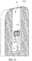
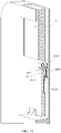
- FIG. 12 is a first schematic diagram of a first state of a conductive elastic piece and an electrical contact assembly in an electronic device according to an embodiment of this application
- FIG. 13 is a second schematic diagram of a first state of a conductive elastic piece and an electrical contact assembly in an electronic device according to an embodiment of this application
- FIG. 14 is a third schematic diagram of a first state of a conductive elastic piece and an electrical contact assembly in an electronic device according to an embodiment of this application.
- the support 41 is located in the accommodating chamber 23, and an upper end face of the support 41 is flush with an outer surface of the middle frame 22. This state may be called a first state of the support 41 or an initial state of the support 41.
- the first contact part 4312 in the first conductive elastic piece 43 is in contact with the second contact part 4223 of the conductive part 422 in the electrical contact assembly 42 to provide stable current conduction support.
- the first contact part 4312 in the first conductive elastic piece 43 first slides on a plane of the second contact part 4223, and after the first contact part 4312 slides out the plane of the second contact part 4223, the second inclined part 4313 of the first contact part 4312 in the first conductive elastic piece 43 continues to be in contact with the guide edge 4224 of the electrical contact assembly 42.
- the first conductive elastic piece 43 slides smoothly, and the first conductive elastic piece 43 has no sudden deformation, thereby guaranteeing the service life of the first conductive elastic piece 43.
- the second conductive elastic piece 43 is suspended in the foregoing process and is not in contact with the electrical contact assembly 42.
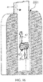
- FIG. 15 is a first schematic diagram of a second state of a conductive elastic piece and an electrical contact assembly in an electronic device according to an embodiment of this application
- FIG. 16 is a second schematic diagram of a second state of a conductive elastic piece and an electrical contact assembly in an electronic device according to an embodiment of this application
- FIG. 17 is a third schematic diagram of a second state of a conductive elastic piece and an electrical contact assembly in an electronic device according to an embodiment of this application.
- the support 41 continues to slide toward the outside of the accommodating chamber 23, and the first conductive elastic piece 43 is out of contact with the conductive part 422 in the electrical contact assembly 42.
- FIG. 18 is a first schematic diagram of a third state of a conductive elastic piece and an electrical contact assembly in an electronic device according to an embodiment of this application
- FIG. 19 is a second schematic diagram of a third state of a conductive elastic piece and an electrical contact assembly in an electronic device according to an embodiment of this application
- FIG. 20 is a third schematic diagram of a third state of a conductive elastic piece and an electrical contact assembly in an electronic device according to an embodiment of this application.
- This state may be called a second state of the support 41 or an end state of the support 41.
- the first contact part 4312 in the second conductive elastic piece 43 first slides on a plane of the second contact part 4223, and after the first contact part 4312 slides out the plane of the second contact part 4223, the second inclined part 4313 of the first contact part 4312 in the second conductive elastic piece 43 continues to be in contact with the guide edge 4224 of the electrical contact assembly 42.
- the second conductive elastic piece 43 slides smoothly and has no sudden deformation, thereby guaranteeing the service life of the second conductive elastic piece 43.
- the first conductive elastic piece 43 is suspended in the foregoing process and is not in contact with the electrical contact assembly 42.
- the two conductive elastic pieces 43 are always not in contact with the metal middle plate 221 or the conductive part 422 during sliding of the support 41, so as to prevent unstable electrical connection during the sliding of the support 41.
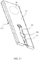
- FIG. 21 is a schematic structural diagram of a conductive elastic piece and a support in an electronic device according to another embodiment of this application; and FIG. 22 is a schematic structural diagram of a conductive elastic piece in an electronic device according to another embodiment of this application.
- this embodiment provides a mobile phone 100 based on Embodiment 1.
- the structure of this embodiment is different from the structure of the conductive elastic piece 43 and the accommodating groove 411 in the mobile phone 100 in Embodiment 1, and the rest of the structure is the same.
- the part of this embodiment the same as that of Embodiment 1 is described in detail in Embodiment 1. Details are not described in this embodiment again.
- two conductive elastic pieces 43 are located on the same straight line.
- the two conductive elastic pieces 43 are symmetrically disposed, and fixed ends 432 of the two conductive elastic pieces 43 are connected to each other.
- first accommodating parts 4111 of the two accommodating grooves 411 which are configured to accommodate the fixed ends 432, are connected to each other.
- the two conductive elastic pieces 43 are integrated, so that the two conductive elastic pieces 43 may be integrally formed, which facilitates machining of the two conductive elastic pieces 43.
- this embodiment saves parts in the mobile phone 100 and space.
- FIG. 23 is a schematic structural diagram of a conductive elastic piece and a support in an electronic device according to another embodiment of this application
- FIG. 24 is a schematic structural diagram of a conductive elastic piece in an electronic device according to another embodiment of this application
- FIG. 25 is a cross-sectional view taken along F-F in FIG. 23 .
- this embodiment provides a mobile phone 100 based on Embodiment 1.
- the structure of this embodiment is different from the structure of the conductive elastic piece 43 and the accommodating groove 411 in the mobile phone 100 in Embodiment 1, and the rest of the structure is the same.
- the part of this embodiment the same as that of Embodiment 1 is described in detail in Embodiment 1. Details are not described in this embodiment again.
- two conductive elastic pieces 43 are located on the same straight line.
- the two conductive elastic pieces 43 are symmetrically disposed, and fixed ends 432 of the two conductive elastic pieces 43 are connected to each other.
- first accommodating parts 4111 of the two accommodating grooves 411 which are configured to accommodate the fixed ends 432, are connected to each other.
- the two conductive elastic pieces 43 are integrated, so that the two conductive elastic pieces 43 may be integrally formed, which facilitates machining of the two conductive elastic pieces 43.
- this embodiment saves parts in the mobile phone 100 and space.
- the fixed end 432 may be rectangular, annular or circular, and the first accommodating part 4111 in the corresponding accommodating groove 411 is also rectangular or circular.
- the fixed end 432 is provided with a mounting hole 4321, and the first accommodating part 4111 is provided with a blind hole, and a screw runs through the mounting hole 4321 and is screwed into the blind hole to connect the conductive elastic piece 43 into the accommodating groove 411.
- a surface of each of the mounting holes 4321 facing the first accommodating part 4111 is provided with at least one protruding point 4322, and each protruding point 4322 may be formed by stamping.
- a face of the protruding point 4322 in contact with the first accommodating part 4111 may be electroplated with pure gold or nickel to reduce impedance of a contact point between the protruding point 4322 and the first accommodating part 4111.
- the two conductive elastic pieces 43 are integrated, so that the two conductive elastic pieces 43 may be integrally formed, which facilitates machining of the two conductive elastic pieces 43.
- this embodiment saves parts in the mobile phone 100 and space.
- FIG. 26 is a schematic internal structural diagram of an electronic device according to an embodiment of this application
- FIG. 27 is a schematic structural diagram of a middle frame in an electronic device according to an embodiment of this application
- FIG. 28 is a schematic structural diagram of a middle frame in another direction in an electronic device according to an embodiment of this application.
- this embodiment provides a mobile phone 100 on the basis of any of the foregoing embodiments, and the elastic piece assembly 40 in any of the foregoing embodiments can be applied to the mobile phone 100 which slides as a whole.
- a housing 20 of the mobile phone 100 includes a sliding housing 24, a middle frame 22, and a rear cover 21.
- the rear cover 21 is connected to the middle frame 22, and the sliding housing 24 slides relative to the rear cover 21 or the middle frame 22. That is, the first component 300 is the middle frame 22 or the rear cover 21, and the second component 400 is the sliding housing 24.
- the support 41 does not need to be provided, the accommodating groove 411 is located on the sliding housing 24, the two conductive elastic pieces 43 are connected to the sliding housing 24, and the electrical contact assembly 42 is located on the middle frame 22.
- the sliding housing 24 slides relative to the rear cover 21 or the middle frame 22, and a stable electrical connection between the middle frame 22 and the sliding housing 24 is realized through contact between the conductive elastic pieces 43 and the electrical contact assembly 42.
- the first component 300 may alternatively be the sliding housing 24, and the second component 400 may be the middle frame 22 or the rear cover 21. This is not limited in this embodiment.
- the support 41 is not provided, the two conductive elastic pieces 43 are connected to the sliding housing 24, and the electrical contact assembly 42 is located on the middle frame 22.
- the rest of the structure is the same as that of any of the foregoing embodiments.
- the part of this embodiment the same as that of any of the foregoing embodiments is described in detail in the foregoing embodiment. Details are not described in this embodiment again.
- the elastic piece assembly 40 in the foregoing embodiment is not limited to a mobile phone 100 that is provided with a slidable camera assembly 30 or slides as a whole, and can also be used for other slidable structures inside the mobile phone 100, such as grounding of lines in the mobile phone 100. Details are not described in this embodiment again.
Landscapes
- Engineering & Computer Science (AREA)
- Signal Processing (AREA)
- Multimedia (AREA)
- Physics & Mathematics (AREA)
- General Physics & Mathematics (AREA)
- Telephone Set Structure (AREA)
Abstract
Description
- This application claims priority to
Chinese Patent Application No. 201911164728.7, filed with China National Intellectual Property Administration on November 25, 2019 - Embodiments of this application relate to the field of electronic devices, and in particular, to an elastic piece assembly and an electronic device with an elastic piece assembly.
- With the development of communications technologies, electronic devices such as smartphones and tablet computers are playing an increasingly important role in people's daily life. Components inside the electronic device need to be connected to each other, and the connection between the components is required to be stable to meet requirements for resistance, stability, and the like. Therefore, a conductive elastic piece is arranged inside the electronic device, and the components are connected by using the elastic piece. As a connecting medium between different media or electronic circuits, the elastic piece can be used to enable connection of electric signals, connection of antennas or grounding connection.
-
FIG. 1 is a schematic diagram of a structure in which relatively moving components are electrically connected to each other by using elastic pieces in the prior art. As shown inFIG. 1 , the structure includes a first component, a second component and two elastic pieces. One end of each of the elastic pieces is arranged on the first component, and the other end of each of the elastic pieces is a free end and is bent toward the second component. Two connecting contacts are arranged on the second component, and the two connecting contacts are located in a direction of relative movement of the first component and the second component. A bend apex of the first elastic piece is in contact with the first connecting contact. With relative movement of the first component and the second component, the bend apex of the first elastic piece is out of contact with the first connecting contact until a bend apex of the second elastic piece moves and comes into contact with the second connecting contact. - However, it is difficult to control deformation of the elastic pieces. When an elastic force of the elastic pieces is small, the contact is unstable. When the elastic force is large, friction between the first component and the second component will increase, thereby affecting relative sliding between the first component and the second component.
- Embodiments of this application provide an elastic piece assembly and an electronic device with an elastic piece assembly, so that deformation of each conductive elastic piece can be controlled to ensure that an electrical contact section of the conductive elastic piece has enough elasticity to be in contact with an electrical contact assembly, and the conductive elastic piece is prevented from affecting relative sliding between a first component and a second component.
- According to a first aspect, an embodiment of this application provides an elastic piece assembly applied to an electronic device, where the electronic device includes a first component and a second component that are capable of sliding relatively in a first direction, and the elastic piece assembly includes a support, an electrical contact assembly, and at least two conductive elastic pieces;
- the electrical contact assembly is configured to be connected to the first component, and the support is configured to be connected to the second component; and
- two ends of each of the conductive elastic pieces are connected to the support, the conductive elastic piece is provided with an electrical contact section bent toward the electrical contact assembly, and the electrical contact section is located between two end portions of the conductive elastic piece; the conductive elastic pieces are separately and sequentially arranged in the first direction, and when the first component and the second component slide relatively, the electrical contact assembly abuts against the electrical contact sections of different conductive elastic pieces to connect the electrical contact assembly to the conductive elastic pieces. In this application, the two ends of each of the conductive elastic pieces are connected to the support, so that deformation of the conductive elastic piece is controlled to ensure that the electrical contact section of the conductive elastic piece has enough elasticity to be in contact with the electrical contact assembly, and the conductive elastic piece is prevented from affecting relative sliding between the support and a metal middle plate.
- In an optional manner, in the elastic piece assembly according to this embodiment of this application, the conductive elastic pieces each include a fixed end fixedly connected to the support and a connecting end movably connected to the support, and the electrical contact section protrudes toward the electrical contact assembly; and
the connecting end is capable of moving relative to the support to limit a protrusion height of the electrical contact section relative to the support. In this application, the fixed end is fixedly connected to the support, so that the conductive elastic piece can be reliably connected to the support. The electrical contact section connected to the fixed end is configured to be in electrical contact with the electrical contact assembly, to connect the conductive elastic piece to the electrical contact assembly. The connecting end connected to the electrical contact section moves relative to the support to limit the protrusion height of the electrical contact section relative to the support. - In an optional manner, in the elastic piece assembly according to this embodiment of this application, the support is provided with an accommodating groove, each of the conductive elastic pieces is located in the accommodating groove, and the connecting end is capable of moving in the accommodating groove to limit deformation of the conductive elastic piece. The accommodating grooves are provided to accommodate the conductive elastic pieces, so that part or all of the fixed end and the connecting end of each of the conductive elastic pieces is located in the accommodating groove, and a bending point in the electrical contact section can extend out of the accommodating groove.
- In an optional manner, in the elastic piece assembly according to this embodiment of this application, the accommodating groove includes a first accommodating part, a guide part and a second accommodating part that communicate with each other in sequence, the fixed end is located in the first accommodating part and connected to the first accommodating part, and the connecting end is located in the second accommodating part. This facilitates installation of the conductive elastic piece and can prevent reverse installation of the conductive elastic piece.
- In an optional manner, in the elastic piece assembly according to this embodiment of this application, the second accommodating part is internally provided with two extended sections extending toward opposite sides of the support respectively, two opposite sides of the connecting end are provided with extended buckles, and the extended buckles are located in the extended sections. The extended sections are arranged in the second accommodating part, the connecting end is provided with the extended buckles, and the extended buckles each are located in the extended section and match the extended section, so that the extended buckle can move in the extended section in the first direction to limit deformation of the conductive elastic piece. This enables the support to slide smoothly, and ensures conductive stability of the conductive elastic piece.
- In an optional manner, in the elastic piece assembly according to this embodiment of this application, the electrical contact section includes a first inclined part, a first contact part and a second inclined part that are connected in sequence, the first contact part abuts against the electrical contact assembly, and the first inclined part and the second inclined part are inclined toward the electrical contact assembly. The first inclined part and the second inclined part are arranged on the electrical contact section to serve as a buffer for the conductive elastic piece in a sliding process, so that the first contact part gradually slides to a position in contact with the electrical contact assembly. An included angle between the first inclined part and a plane where the fixed end is located is greater than or equal to 10° and less than or equal to 70°, and an included angle between the second inclined part and a plane where the fixed end is located is greater than or equal to 10° and less than or equal to 70°. Larger included angles indicate a better buffering effect on the conductive elastic piece in the sliding process.
- In an optional manner, in the elastic piece assembly according to this embodiment of this application, the first contact part is provided with a plating layer for reducing impedance of the first contact part.
- In an optional manner, in the elastic piece assembly according to this embodiment of this application, there are two conductive elastic pieces, the electrical contact sections of the two conductive elastic pieces face opposite directions, the two conductive elastic pieces are parallel to the first direction, and a distance between the electrical contact sections of the two conductive elastic pieces is equal to a sliding distance between the first component and the second component.
- In an optional manner, in the elastic piece assembly according to this embodiment of this application, the two conductive elastic pieces are staggered in the first direction, or the two conductive elastic pieces are located on the same straight line. When the two conductive elastic pieces are staggered in the first direction, the first contact parts of the two conductive elastic pieces are in contact with different positions of the electrical contact assembly, respectively. In this way, wear of the electrical contact assembly and the conductive elastic piece can be prevented, and service lives of the electrical contact assembly and the conductive elastic piece can be prolonged.
- In an optional manner, in the elastic piece assembly according to this embodiment of this application, when the two conductive elastic pieces are located on the same straight line, the fixed ends of the two conductive elastic pieces are connected to each other.
- In an optional manner, in the elastic piece assembly according to this embodiment of this application, the electrical contact assembly includes a mounting frame and a conductive part connected to the mounting frame, the mounting frame is configured to be connected to the first component, and each of the electrical contact sections abuts against the conductive part.
- In an optional manner, in the elastic piece assembly according to this embodiment of this application, at least one side of the conductive part is provided with at least one positioning notch, and the mounting frame is provided with a positioning part matching the positioning notch.
- In an optional manner, in the elastic piece assembly according to this embodiment of this application, the conductive part is provided with at least one bent part bent toward the mounting frame, and each of the bent parts abuts against an end portion of the mounting frame when the conductive part is connected to the mounting frame.
- In an optional manner, in the elastic piece assembly according to this embodiment of this application, the conductive part includes a second contact part and guide edges each connected to an edge of the second contact part, each of the first contact parts abuts against the second contact part, the guide edge is inclined toward the mounting frame, and an extension direction of the guide edge is perpendicular to the first direction. To prevent interference between the positioning part and the bent part, the positioning notch and the bent part on the conductive part are located on different sides of the conductive part respectively.
- In an optional manner, in the elastic piece assembly according to this embodiment of this application, there are at least two guide edges, the guide edges are located on opposite sides of the second contact part respectively, and an included angle between each of the guide edges and the second contact part is 10°-70°. A larger included angle between the guide edge and the second contact part indicates a better buffering effect.
- In an optional manner, in the elastic piece assembly according to this embodiment of this application, the positioning notch is located on the guide edge. An arc is arranged at an intersection of the second contact part and the guide edge. The arc can also buffer the conductive elastic piece in a relative movement process, which prevents scratching in the sliding process, thereby prolonging the service life of the conductive elastic piece.
- According to a second aspect, an embodiment of this application further provides an electronic device with an elastic piece assembly, including a first component, a second component and the elastic piece assembly according to the foregoing embodiment, where the first component is connected to the second component by using the elastic piece assembly.
- In an optional manner, in the electronic device according to this embodiment of this application, the first component is a camera assembly and the second component is a middle frame; or the first component is a middle frame and the second component is a camera assembly.
- In an optional manner, in the electronic device according to this embodiment of this application, the first component is a sliding housing and the second component is a fixed housing; or the first component is a fixed housing and the second component is a sliding housing.
- This application provides the elastic piece assembly and the electronic device with an elastic piece assembly. In the elastic piece assembly, the two ends of each of the conductive elastic pieces are connected to the support, so that deformation of the conductive elastic piece is controlled to ensure that the electrical contact section of the conductive elastic piece has enough elasticity to be in contact with the electrical contact assembly, and the conductive elastic piece is prevented from affecting relative sliding between the first component and the second component.
-
-
FIG. 1 is a schematic diagram of a structure in which relatively moving components are electrically connected to each other by using elastic pieces in the prior art; -
FIG. 2 is a schematic structural diagram of an electronic device according to an embodiment of this application; -
FIG. 3 is a side view of an electronic device according to an embodiment of this application; -
FIG. 4 is an exploded view of an electronic device according to an embodiment of this application; -
FIG. 5 is a schematic structural diagram of a conductive elastic piece in an electronic device according to an embodiment of this application; -
FIG. 6 is a schematic structural diagram of a conductive elastic piece and a support in an electronic device according to an embodiment of this application; -
FIG. 7 is a schematic structural diagram of a conductive elastic piece and a support in another direction in an electronic device according to an embodiment of this application; -
FIG. 8 is an arrangement diagram of conductive elastic pieces in an electronic device according to an embodiment of this application; -
FIG. 9 is a schematic internal structural diagram of a housing in an electronic device according to an embodiment of this application; -
FIG. 10 is a partial enlarged diagram of a position C inFIG. 9 ; -
FIG. 11 is a schematic structural diagram of a conductive part of an electrical contact assembly in an electronic device according to an embodiment of this application; -
FIG. 12 is a first schematic diagram of a first state of a conductive elastic piece and an electrical contact assembly in an electronic device according to an embodiment of this application; -
FIG. 13 is a second schematic diagram of a first state of a conductive elastic piece and an electrical contact assembly in an electronic device according to an embodiment of this application; -
FIG. 14 is a third schematic diagram of a first state of a conductive elastic piece and an electrical contact assembly in an electronic device according to an embodiment of this application; -
FIG. 15 is a first schematic diagram of a second state of a conductive elastic piece and an electrical contact assembly in an electronic device according to an embodiment of this application; -
FIG. 16 is a second schematic diagram of a second state of a conductive elastic piece and an electrical contact assembly in an electronic device according to an embodiment of this application; -
FIG. 17 is a third schematic diagram of a second state of a conductive elastic piece and an electrical contact assembly in an electronic device according to an embodiment of this application; -
FIG. 18 is a first schematic diagram of a third state of a conductive elastic piece and an electrical contact assembly in an electronic device according to an embodiment of this application; -
FIG. 19 is a second schematic diagram of a third state of a conductive elastic piece and an electrical contact assembly in an electronic device according to an embodiment of this application; -
FIG. 20 is a third schematic diagram of a third state of a conductive elastic piece and an electrical contact assembly in an electronic device according to an embodiment of this application; -
FIG. 21 is a schematic structural diagram of a conductive elastic piece and a support in an electronic device according to an embodiment of this application; -
FIG. 22 is a schematic structural diagram of a conductive elastic piece in an electronic device according to an embodiment of this application; -
FIG. 23 is a schematic structural diagram of a conductive elastic piece and a support in an electronic device according to an embodiment of this application; -
FIG. 24 is a schematic structural diagram of a conductive elastic piece in an electronic device according to an embodiment of this application; -
FIG. 25 is a cross-sectional view taken along F-F inFIG. 23 ; -
FIG. 26 is a schematic internal structural diagram of an electronic device according to an embodiment of this application; -
FIG. 27 is a schematic structural diagram of a middle frame in an electronic device according to an embodiment of this application; and -
FIG. 28 is a schematic structural diagram of a middle frame in another direction in an electronic device according to an embodiment of this application. - Description of reference numerals:
- 100: mobile phone; 10: display screen; 20: housing; 21: rear cover; 22: middle frame; 23: accommodating chamber; 24: sliding housing; 221: metal middle plate; 222: bezel; 2221: through hole; 30: camera assembly; 40: elastic piece assembly; 41: support; 411: accommodating groove; 4111: first accommodating part; 4112: guide part; 4113: second accommodating part; 4114: extended section; 412: stepped surface; 42: electrical contact assembly; 421: mounting frame; 4211: positioning part; 422: conductive part; 4221: positioning notch; 4222: bent part; 4223: second contact part; 4224: guide edge; 43: conductive elastic piece; 431: electrical contact section; 4311: first inclined part; 4312: first contact part; 4313: second inclined part; 432: fixed end; 4321 mounting hole; 4322: protruding point; 433: connecting end; 4331: extended buckle;
- 200: elastic piece; 300: first component; 400: second component; 500: connecting contact.
- Terms used in the implementations of this application are only used to explain specific embodiments of this application, but are not intended to limit this application. Implementations of embodiments of this application are described in detail with reference to the accompanying drawings.
- An embodiment of this application provides an electronic device, including but not limited to a mobile or fixed terminal with a display screen and a housing, such as a mobile phone, a tablet computer, a notebook computer, an ultra-mobile personal computer (ultra-mobile personal computer, UMPC), a netbook, a POS machine, a personal digital assistant (personal digital assistant, PDA), a wearable device and a virtual reality device.
-
FIG. 1 is a schematic diagram of a structure in which relatively moving components are electrically connected to each other by using elastic pieces in the prior art. As shown inFIG. 1 , the structure includes afirst component 300, asecond component 400 and twoelastic pieces 200. One end of each of theelastic pieces 200 is arranged on thefirst component 300, and the other end of each of theelastic pieces 200 is a free end and is bent toward thesecond component 400. Two connectingcontacts 500 are arranged on thesecond component 400, and the two connectingcontacts 500 are located in a direction of relative movement of thefirst component 300 and thesecond component 400. A bend apex of the firstelastic piece 200 is in contact with the first connectingcontact 500. With relative movement of thefirst component 300 and thesecond component 400, the bend apex of the firstelastic piece 200 is out of contact with the first connectingcontact 500 until a bend apex of the secondelastic piece 200 moves and comes into contact with the second connectingcontact 500. However, it is difficult to control deformation of theelastic pieces 200. When an elastic force of theelastic pieces 200 is small, the contact is unstable. When the elastic force is large, friction between thefirst component 300 and thesecond component 400 will increase, thereby affecting relative sliding between thefirst component 300 and thesecond component 400. - To resolve the foregoing problems, an embodiment of this application provides an electronic device. When a
support 41 in the electronic device is located in anaccommodating chamber 23, anelectrical contact section 431 on a first conductiveelastic piece 43 on thesupport 41 is in contact with anelectrical contact assembly 42. A driving assembly drives thesupport 41 to slide, so that thesecond component 400 on thesupport 41 extends out of theaccommodating chamber 23 through the throughhole 2221. In the process in which thesecond component 400 extends out of theaccommodating chamber 23, theelectrical contact section 431 on the first conductiveelastic piece 43 is gradually out of contact with theelectrical contact assembly 42 until theelectrical contact section 431 on the second conductiveelastic piece 43 on thesupport 41 comes into contact with theelectrical contact assembly 42, so that thesecond component 400 is still electrically connected to a battery of amobile phone 100. Two ends of each of the conductiveelastic pieces 43 are connected to thesupport 41, so that deformation of the conductiveelastic piece 43 is controlled to ensure that theelectrical contact section 431 of the conductiveelastic piece 43 has enough elasticity to be in contact with theelectrical contact assembly 42, and the conductiveelastic piece 43 is prevented from affecting relative sliding between thesecond component 400 and thefirst component 300. - The electronic device according to this application is described in detail by using the following specific embodiments, which can be combined with each other. The same or similar contents are not described in different embodiments again. For ease of description, the
mobile phone 100 is used as an example of the terminal to describe the following embodiments in detail. -
FIG. 2 is a schematic structural diagram of an electronic device according to an embodiment of this application; andFIG. 3 is a side view of an electronic device according to an embodiment of this application. As shown inFIG. 2 andFIG. 3 , themobile phone 100 according to this embodiment of this application may include adisplay screen 10, ahousing 20, and acamera assembly 30. Thedisplay screen 10 is connected to thehousing 20, and thecamera assembly 30 is located on thehousing 20. - The
display screen 10 may be an organic light-emitting diode (organic light-emitting diode, OLED) display screen or a liquid crystal display (liquid crystal display, LCD). It should be understood that thedisplay screen 10 may include a display and a touch device. The display is configured to output display content to a user, and the touch device is configured to receive a touch event input by the user on thedisplay screen 10. - The
housing 20 may include arear cover 21 and amiddle frame 22. Themiddle frame 22 is located between thedisplay screen 10 and therear cover 21. Thedisplay screen 10 is connected to one side of themiddle frame 22, and therear cover 21 is connected to the other side of themiddle frame 22. Thedisplay screen 10, therear cover 21 and themiddle frame 22 jointly enclose theaccommodating chamber 23. Theaccommodating chamber 23 contains a battery, a circuit board, a communications module (not shown in the figure), and the like. - When the battery is arranged on the
middle frame 22, for example, a battery compartment may be arranged on one side of themiddle frame 22 facing therear cover 21, and the battery is installed in the battery compartment. In this embodiment of this application, the battery can be connected to a charging management module and the circuit board by using a power management module, and the power management module receives an input of the battery and/or the charging management module and supplies power to the processor, an internal memory, an external memory, thedisplay screen 10, thecamera assembly 30, the communications module, and the like. The power management module may be further configured to monitor battery capacity, battery cycle times, battery health statuses (leakage and impedance) and other parameters. In some other embodiments, the power management module may alternatively be disposed in the processor of the circuit board. In some other embodiments, the power management module and the charging management module may alternatively be arranged in the same device. - The
middle frame 22 may include a metalmiddle plate 221 and abezel 222. One round ofbezel 222 is disposed around an edge of the metalmiddle plate 221. When the assembly is completed, thebezel 222 is located between thedisplay screen 10 and therear cover 21, and thebezel 222 is exposed to the outside. Thedisplay screen 10, therear cover 21 and thebezel 222 jointly enclose theaccommodating chamber 23, and themiddle frame 22 is located in theaccommodating chamber 23. - In this embodiment of this application, the material of the metal
middle plate 221 may include, but is not limited to, aluminum alloy, stainless steel, a steel-aluminum composite die-casting plate or titanium alloy. Thebezel 222 may be a metal bezel, or thebezel 222 may alternatively be a non-metal bezel, such as a ceramic bezel or a glass bezel. When thebezel 222 is a metal bezel, the material of the metal bezel includes, but is not limited to, aluminum alloy, stainless steel or titanium alloy. Therear cover 21 may be a metal rear cover, a glass rear cover, a plastic rear cover or a ceramic rear cover. In this embodiment of this application, the material of therear cover 21 is not limited. - Specifically, the
first component 300 may be thehousing 20 and thesecond component 400 may be thecamera assembly 30. Thecamera assembly 30 may include a front camera and/or a rear camera, a flash, a miniature projection apparatus, and the like. Details are not described herein again. In some embodiments, thecamera assembly 30 may be located in theaccommodating chamber 23. For example, the front camera is disposed in theaccommodating chamber 23, and when in use, by sliding the front camera, the front camera slides relative to thehousing 20, so that the front camera extends out of theaccommodating chamber 23, so as to perform operations such as photographing or video shooting. The front camera is hidden in theaccommodating chamber 23, so that a screen-to-body ratio is increased, which makes it easier to obtain a good visual impression in the appearance design of themobile phone 100. The rear camera may alternatively be disposed in theaccommodating chamber 23, and when in use, by sliding the rear camera, the rear camera slides relative to thehousing 20, so that the rear camera extends out of theaccommodating chamber 23, so as to perform operations such as photographing or video shooting. -
FIG. 4 is an exploded view of an electronic device according to an embodiment of this application. As shown inFIG. 3 and FIG. 4 , in this embodiment of this application, to enable thecamera assembly 30 to maintain electrical contact with the battery and the circuit board in theaccommodating chamber 23 after sliding out of theaccommodating chamber 23 relative to thehousing 20, themobile phone 100 may further include anelastic piece assembly 40. - Specifically, the
elastic piece assembly 40 includes asupport 41, anelectrical contact assembly 42 and at least two conductiveelastic pieces 43. Theelectrical contact assembly 42 is connected to thehousing 20, and thesupport 41 is connected to thecamera assembly 30. - Two ends of each of the conductive
elastic pieces 43 are connected to thesupport 41, the conductiveelastic piece 43 is provided with anelectrical contact section 431 bent toward theelectrical contact assembly 42, and theelectrical contact section 431 is located between two end portions of the conductiveelastic piece 43; the conductiveelastic pieces 43 are separately and sequentially arranged in the first direction, and when thehousing 20 and thecamera assembly 30 slide relatively, theelectrical contact assembly 42 abuts against the electrical contact sections of different conductiveelastic pieces 43 to connect theelectrical contact assembly 42 to the conductiveelastic pieces 43. - In the foregoing
elastic piece assembly 40, theelectrical contact assembly 42 is connected to the circuit board in thehousing 20, the circuit board is connected to the battery, the circuit board in thehousing 20 supplies power to theelectrical contact assembly 42, and when thecamera assembly 30 and thehousing 20 slide relatively, or when thecamera assembly 30 and thehousing 20 are both in a relatively static state, theelectrical contact assembly 42 is kept in a charged state. - To fix the
camera assembly 30, theelastic piece assembly 40 may further include asupport 41, and thesupport 41 supports thecamera assembly 30. To connect thecamera assembly 30 to thesupport 41 conveniently, a first connecting part may be disposed on thesupport 41 and a second connecting part may be disposed on thecamera assembly 30, and the first connecting part is connected to the second connecting part through bonding, clamping or screw connection, or the like, so that thecamera assembly 30 is installed on thesupport 41. The material of thesupport 41 may be the same as that of thebezel 222, and the material of thesupport 41 may alternatively be different from that of thebezel 222. This is not limited in this embodiment. - Specifically, the
support 41 may be divided into two parts, which are an upper half of thesupport 41 and a lower half of thesupport 41. Thecamera assembly 30 is located on the upper half of thesupport 41, and the upper half of thesupport 41 can extend out of theaccommodating chamber 23 to drive thecamera assembly 30 to extend out of theaccommodating chamber 23. The lower half of thesupport 41 is configured to be connected to the conductiveelastic piece 43, and when thecamera assembly 30 slides relative to thehousing 20, the lower half of thesupport 41 is located in theaccommodating chamber 23. This prevents a situation that the conductiveelastic piece 43 located in the lower half of thesupport 41 extends out of theaccommodating chamber 23 and is corroded by water vapor and the like outside theaccommodating chamber 23, thereby affecting conductive performance of the conductiveelastic piece 43. Thecamera assembly 30 can be embedded in the upper half of thesupport 41, so as to avoid increasing the overall thickness of themobile phone 100, and thecamera assembly 30 can be reliably connected in thesupport 41. Because thecamera assembly 30 is disposed in the upper half of thesupport 41, a thickness of the upper half of thesupport 41 may be greater than that of the lower half of thesupport 41. A steppedsurface 412 is formed due to a thickness difference at a joint between the upper half of thesupport 41 and the lower part of thesupport 41. The steppedsurface 412 can also be used as a limiting part for thecamera assembly 30 to extend out of theaccommodating chamber 23. An abutting part may be disposed in theaccommodating chamber 23. When the steppedsurface 412 moves to the abutting part of theaccommodating chamber 23, the steppedsurface 412 abuts against the abutting part, thereby preventing thesupport 41 from continuing movement. In this case, thecamera assembly 30 is completely removed from theaccommodating chamber 23. - To enable the
support 41 to slide smoothly and extend out of theaccommodating chamber 23, thebezel 222 is provided with a throughhole 2221 for thesupport 41 to enter or exit theaccommodating chamber 23. Thesupport 41 extends out of theaccommodating chamber 23 through the throughhole 2221, and thesupport 41 drives thecamera assembly 30 to extend out of theaccommodating chamber 23 through the throughhole 2221. The throughhole 2221 is located in thebezel 222. That is, thesupport 41 slides relative to the metalmiddle plate 221 so that thecamera assembly 30 slides relative to thehousing 20. A driving assembly may be disposed in theaccommodating chamber 23, the driving assembly may be disposed on the metalmiddle plate 221, and thesupport 41 may be connected to the driving assembly in theaccommodating chamber 23. Thesupport 41 is driven by the driving assembly to slide to extend out of or enter theaccommodating chamber 23. The driving assembly may include an electromagnetic telescopic motor. To enable thesupport 41 to slide smoothly, a guide rail may further be disposed in theaccommodating chamber 23. Other driving assemblies may alternatively be used to drive thesupport 41 to extend out of or enter theaccommodating chamber 23. This is not limited in this embodiment. - Specifically, an inner sidewall of the through
hole 2221 matches an outer sidewall of thesupport 41. For example, if the throughhole 2221 is a circular hole, thesupport 41 is at least partially cylindrical, and an outer diameter of thesupport 41 is equal to an inner diameter of the throughhole 2221. Alternatively, when the throughhole 2221 is an elongated hole, thesupport 41 is at least partially a quadrangular prism, and the cross section of thesupport 41 perpendicular to an axial direction of thesupport 41 is the same as a plane enclosed by an inner contour of the throughhole 2221. This prevents a situation that when thesupport 41 slides in and out of theaccommodating chamber 23, foreign matter enters theaccommodating chamber 23, which damages other parts in theaccommodating chamber 23 or blocks thesupport 41, making it difficult for thesupport 41 to smoothly enter and exit theaccommodating chamber 23. When thesupport 41 slides into theaccommodating chamber 23, an end face of thesupport 41 facing an outer side of theaccommodating chamber 23 is flush with an outer side face of thebezel 222, which makes it easier to obtain a good visual impression in the appearance design of themobile phone 100. - The conductive
elastic pieces 43 are separately and sequentially arranged in the first direction. The first direction is a direction of sliding of thesupport 41 relative to thebezel 222, which is also a direction in which thesupport 41 slides out of or enters thebezel 222. Each of the conductiveelastic pieces 43 is connected to thesupport 41, and each of the conductiveelastic pieces 43 is electrically connected to thecamera assembly 30. For example, the first conductiveelastic piece 43 is connected to the front camera in thecamera assembly 30, the second conductiveelastic piece 43 is connected to the rear camera in thecamera assembly 30, the second conductiveelastic piece 43 is connected to the front camera in thecamera assembly 30, and the third conductiveelastic piece 43 is connected to the flash in thecamera assembly 30. The first conductiveelastic piece 43 may be connected to thecamera assembly 30 by using a wire, and the conductiveelastic piece 43 may be connected to thecamera assembly 30 by using a metal sheet. This is not limited in this embodiment. - In the
mobile phone 100 according to this embodiment of this application, when thesupport 41 is located in theaccommodating chamber 23, theelectrical contact section 431 on the first conductiveelastic piece 43 on thesupport 41 is in contact with anelectrical contact assembly 42. The driving assembly drives thesupport 41 to slide, so that thecamera assembly 30 on thesupport 41 extends out of theaccommodating chamber 23 through the throughhole 2221. In the process in which thecamera assembly 30 extends out of theaccommodating chamber 23, theelectrical contact section 431 on the first conductiveelastic piece 43 is gradually out of contact with theelectrical contact assembly 42 until theelectrical contact section 431 on the second conductiveelastic piece 43 on thesupport 41 comes into contact with theelectrical contact assembly 42, so that thecamera assembly 30 is still electrically connected to the battery of themobile phone 100, and thecamera assembly 30 to perform photographing or video shooting. The two ends of each of the conductiveelastic pieces 43 are connected to thesupport 41, so that deformation of the conductiveelastic piece 43 is controlled to ensure that theelectrical contact section 431 of the conductiveelastic piece 43 has enough elasticity to be in contact with theelectrical contact assembly 42, and the conductiveelastic piece 43 is prevented from affecting relative sliding between thesupport 41 and the metalmiddle plate 221. -
FIG. 5 is a schematic structural diagram of a conductive elastic piece in an electronic device according to an embodiment of this application;FIG. 6 is a schematic structural diagram of a conductive elastic piece and a support in an electronic device according to an embodiment of this application; andFIG. 7 is a schematic structural diagram of a conductive elastic piece and a support in another direction in an electronic device according to an embodiment of this application. As shown inFIG. 4 to FIG. 7 , in this embodiment, the conductiveelastic piece 43 includes afixed end 432 fixedly connected to thesupport 41 and a connectingend 433 movably connected to thesupport 41, and theelectrical contact section 431 protrudes toward theelectrical contact assembly 42. The connectingend 433 can move relative to thesupport 41 to limit the protrusion height of theelectrical contact section 431 relative to thesupport 41. - Specifically, the conductive
elastic piece 43 may be divided into three sections that are connected in sequence. The first section of the conductiveelastic piece 43 is thefixed end 432, and thefixed end 432 is fixedly connected to thesupport 41. The second section of the conductiveelastic piece 43 is theelectrical contact section 431, and theelectrical contact section 431 is in electrical contact with theelectrical contact assembly 42. The third section of the conductiveelastic piece 43 is the connectingend 433, and the connectingend 433 is movably connected to thesupport 41, that is, the connectingend 433 can move relative to thesupport 41 to limit the protrusion height of theelectrical contact section 431 relative to thesupport 41. Thefixed end 432, theelectrical contact section 431 and the connectingend 433 are connected in sequence. - To reliably connect the
fixed end 432 to thesupport 41, thefixed end 432 may be flat to increase a contact surface between thefixed end 432 and thesupport 41. Thefixed end 432 may be fixedly connected to thesupport 41 by using a screw, welding or bonding. Theelectrical contact section 431 may be a bent part of the conductiveelastic piece 43, the conductiveelastic piece 43 is bent toward theelectrical contact section 431, and a bending point in theelectrical contact section 431 is in pressure contact with theelectrical contact assembly 42. The bending point in theelectrical contact section 431 may also be called a contact, and the contact is in pressure contact with theelectrical contact assembly 42 to connect the conductiveelastic piece 43 to theelectrical contact assembly 42. The connectingend 433 is movably connected to thesupport 41. When the bending point in theelectrical contact section 431 is in pressure contact with theelectrical contact assembly 42, a distance between the conductiveelastic piece 43 and theelectrical contact assembly 42 is minimum. When theelectrical contact assembly 42 is kept fixed, the connectingend 433 of the conductiveelastic piece 43 moves along thesupport 41 to compress the conductiveelastic piece 43 to lower the height of the conductiveelastic piece 43, so that the distance between the conductiveelastic piece 43 and theelectrical contact assembly 42 is reduced. With the movement of thesupport 41, the bending point in theelectrical contact section 431 is separated from the position in pressure contact with theelectrical contact assembly 42. In this case, the connectingend 433 of the conductiveelastic piece 43 moves along thesupport 41 in a direction opposite to a direction in which the conductiveelastic piece 43 is compressed, and the conductiveelastic piece 43 extends to restore the height of the conductiveelastic piece 43 in the extended state, so that the distance between the conductiveelastic piece 43 and theelectrical contact assembly 42 is maximum. Through the change in the distance between the conductiveelastic piece 43 and theelectrical contact assembly 42, the protrusion height of theelectrical contact section 431 relative to thesupport 41 is limited. - In the
mobile phone 100 according to this embodiment of this application, thefixed end 432 is fixedly connected to thesupport 41, so that the conductiveelastic piece 43 can be reliably connected to thesupport 41. Theelectrical contact section 431 connected to thefixed end 432 is configured to be in electrical contact with theelectrical contact assembly 42, to connect the conductiveelastic piece 43 to theelectrical contact assembly 42. The connectingend 433 connected to theelectrical contact section 431 moves relative to thesupport 41 to limit the protrusion height of theelectrical contact section 431 relative to thesupport 41. - As shown in
FIG. 4 to FIG. 7 , in this embodiment, thesupport 41 is provided with anaccommodating groove 411, each of the conductiveelastic pieces 43 is located in theaccommodating groove 411, and the connectingend 433 is capable of moving in theaccommodating groove 411 to limit deformation of the conductiveelastic piece 43. - In this embodiment, an extending direction of the
accommodating groove 411 may be parallel to the first direction, the conductiveelastic pieces 43 are arranged in theaccommodating groove 411, and thefixed end 432 of each of the conductiveelastic pieces 43 is fixedly connected to the bottom of theaccommodating groove 411. The connectingend 433 of each of the conductiveelastic pieces 43 moves in theaccommodating groove 411 to limit deformation of the conductiveelastic piece 43. There are alternatively two or moreaccommodating grooves 411. The quantity of theaccommodating grooves 411 is equal to the quantity of the conductiveelastic pieces 43, and one conductiveelastic piece 43 is placed in oneaccommodating groove 411. In this way, it is convenient to install the conductiveelastic pieces 43 in theaccommodating grooves 411, and the conductiveelastic pieces 43 do not affect each other during installation. - In this embodiment, no limitation is imposed on the depth of the
accommodating groove 411 in this embodiment, provided that the bending point in theelectrical contact section 431 can be in contact with theelectrical contact assembly 42 when theaccommodating groove 411 accommodates the conductiveelastic piece 43. That is, thefixed end 432 and the connectingend 433 of each of the conductiveelastic pieces 43 are at least partially located in theaccommodating groove 411, and the bending point in theelectrical contact section 431 can extend out of theaccommodating groove 411 and can be in contact with theelectrical contact assembly 42. - In the
mobile phone 100 according to this embodiment of this application, theaccommodating grooves 411 are provided to accommodate the conductiveelastic pieces 43, so that part or all of thefixed end 432 and the connectingend 433 of each of the conductiveelastic pieces 43 is located in theaccommodating groove 411, and the bending point in theelectrical contact section 431 can extend out of theaccommodating groove 411. Theaccommodating grooves 411 are provided to accommodate the conductiveelastic pieces 43 and reduce the overall thickness of themobile phone 100. - In the foregoing embodiment, the conductive
elastic piece 43 is divided into thefixed end 432, theelectrical contact section 431 and the connectingend 433 that are connected in sequence. Thefixed end 432, theelectrical contact section 431 and the connectingend 433 have different functions. To facilitate installation of the conductiveelastic piece 43 and prevent reverse installation of the conductiveelastic piece 43, in this embodiment, theaccommodating groove 411 for accommodating the conductiveelastic piece 43 is divided into different areas. The different areas of theaccommodating groove 411 are described below. - As shown in
FIG. 4 to FIG. 7 , in this embodiment, theaccommodating groove 411 includes a firstaccommodating part 4111, aguide part 4112 and a secondaccommodating part 4113 that communicate with each other in sequence, thefixed end 432 is located in the firstaccommodating part 4111, thefixed end 432 is connected to the firstaccommodating part 4111, and the connectingend 433 is located in the secondaccommodating part 4113. - Specifically, the
fixed end 432 is configured to be connected to the firstaccommodating part 4111, so as to reliably connect thefixed end 432 into the firstaccommodating part 4111. A size of thefixed end 432 can be increased in the conductiveelastic piece 43 to increase a contact area between thefixed end 432 and the firstaccommodating part 4111. That is, a width D1 of thefixed end 432 is greater than a width D2 of the connectingend 433, and the width D2 of the connectingend 433 may be equal to a width D3 of theguide part 4112. Correspondingly, the firstaccommodating part 4111 matches thefixed end 432, and a size of the firstaccommodating part 4111 is greater than that of the secondaccommodating part 4113. Thefixed end 432 may be fixedly connected to the firstaccommodating part 4111 by using a screw, welding or bonding. Thefixed end 432 is electrically connected to the firstaccommodating part 4111, and thecamera assembly 30 is electrically connected to the firstaccommodating part 4111 in thesupport 41, so as to electrically connect the conductiveelastic piece 43 to thecamera assembly 30. The connectingend 433 matches the secondaccommodating part 4113. - In the
mobile phone 100 according to this embodiment of this application, theaccommodating groove 411 includes a firstaccommodating part 4111, aguide part 4112 and a secondaccommodating part 4113 that communicate with each other in sequence, thefixed end 432 is located in the firstaccommodating part 4111, and the connectingend 433 is located in the secondaccommodating part 4113. This facilitates installation of the conductiveelastic piece 43 and can prevent reverse installation of the conductiveelastic piece 43. - An excessively high bending point in the
electrical contact section 431 may increase friction in the sliding process of thesupport 41 and affect smooth sliding of thesupport 41; and an excessively low bending point in theelectrical contact section 431 may cause an insufficient pressure during the operation of the bending point in theelectrical contact section 431 and affect conductive stability of the conductiveelastic piece 43. Therefore, in this embodiment, the secondaccommodating part 4113 is internally provided with twoextended sections 4114 extending toward opposite sides of thesupport 41 respectively, two opposite sides of the connectingend 433 are provided withextended buckles 4331, and theextended buckles 4331 are located in theextended sections 4114. - Specifically, the two
extended sections 4114 may be disposed in a width direction of the second accommodating part 4113 (that is, a width D2 direction of the connecting end 433), the twoextended sections 4114 extend in the width D2 direction of the connectingend 433, and the twoextended sections 4114 extend in opposite directions. Two sides of the connectingend 433 are provided with twoextended buckles 4331, theextended buckles 4331 extend in the width D2 direction of the connectingend 433, and the twoextended buckles 4331 extend in opposite directions. The twoextended buckles 4331 may be flush with an end portion of the connectingend 433. - In the
mobile phone 100 according to this embodiment of this application, theextended sections 4114 are arranged in the secondaccommodating part 4113, the connectingend 433 is provided with theextended buckles 4331, and theextended buckles 4331 each are located in theextended section 4114 and match theextended section 4114, so that theextended buckle 4331 can move in theextended section 4114 in the first direction to limit deformation of the conductiveelastic piece 43. This enables thesupport 41 to slide smoothly, and ensures conductive stability of the conductiveelastic piece 43. - As shown in
FIG. 4 andFIG. 5 , in this embodiment, theelectrical contact section 431 includes a firstinclined part 4311, afirst contact part 4312 and a secondinclined part 4313 that are connected in sequence. Thefirst contact part 4312 abuts against theelectrical contact assembly 42, and the firstinclined part 4311 and the secondinclined part 4313 are inclined toward theelectrical contact assembly 42. - Specifically, the
electrical contact section 431 may be formed through bending, the bending point of theelectrical contact section 431 is thefirst contact part 4312, thefirst contact part 4312 is in contact with theelectrical contact assembly 42, the firstinclined part 4311 may be connected to thefixed end 432, the secondinclined part 4313 may be connected to the connectingend 433, and the firstinclined part 4311 and the secondinclined part 4313 are inclined toward theelectrical contact assembly 42. The firstinclined part 4311 and the secondinclined part 4313 are arranged on theelectrical contact section 431 to serve as a buffer for the conductiveelastic piece 43 in the sliding process, so that thefirst contact part 4312 gradually slides to a position in contact with theelectrical contact assembly 42. - An angle at which the first
inclined part 4311 is inclined toward theelectrical contact assembly 42 and an angle at which the secondinclined part 4313 is inclined toward theelectrical contact assembly 42 may be the same or different. This is not limited in this embodiment. - Specifically, an included angle A between the first
inclined part 4311 and a plane where thefixed end 432 is located is greater than or equal to 10° and less than or equal to 70°, and an included angle B between the secondinclined part 4313 and a plane where thefixed end 432 is located is greater than or equal to 10° and less than or equal to 70°. The included angle A between the firstinclined part 4311 and the plane where thefixed end 432 is located is an included angle in an anticlockwise direction between the firstinclined part 4311 and the plane where thefixed end 432 is located, and the included angle B between the secondinclined part 4313 and the plane where thefixed end 432 is located is an included angle in a clockwise direction between the secondinclined part 4313 and the plane where thefixed end 432 is located. A larger included angle A and included angle B indicate a better buffering effect on the conductiveelastic piece 43 in the sliding process. However, a larger included angle A and included angle B also indicate a corresponding increase in the length of the conductiveelastic piece 43. - The
first contact part 4312 in theelectrical contact section 431 is configured to be in contact with theelectrical contact assembly 42. To reduce impedance of thefirst contact part 4312, thefirst contact part 4312 is provided with a plating layer for reducing impedance of thefirst contact part 4312. Impedance (electrical impedance) is the general term for resistance, inductance and capacitance in a circuit that hinder an alternating current. Specifically, a surface of thefirst contact part 4312 may be electroplated with pure gold or nickel and the like, so as to reduce impedance of thefirst contact part 4312. The surface of theelectrical contact section 431 or the surface of the entire conductiveelastic piece 43 may alternatively electroplated with pure gold or nickel. This is not limited in this embodiment. - As shown in
FIG. 4 to FIG. 7 , in this embodiment, there are two conductiveelastic pieces 43, theelectrical contact sections 431 of the two conductiveelastic pieces 43 face opposite directions, the two conductiveelastic pieces 43 are both parallel to the first direction, and a distance between theelectrical contact sections 431 of the two conductiveelastic pieces 43 is equal to a sliding distance between thefirst component 300 and thesecond component 400. - Specifically, the two conductive
elastic pieces 43 are located in differentaccommodating grooves 411 respectively, and the two conductiveelastic pieces 43 are parallel to each other. The two conductiveelastic pieces 43 may face the same direction, that is, theelectrical contact sections 431 of the two conductiveelastic pieces 43 may both face the throughhole 2221. The two conductiveelastic pieces 43 may alternatively face different directions, that is, theelectrical contact sections 431 of the two conductiveelastic pieces 43 face opposite directions. A relative positional relationship between the two conductiveelastic pieces 43 is related to a designed sliding distance of thesupport 41. Specifically, the distance between thefirst contact parts 4312 of the two conductiveelastic pieces 43 in the first direction is equal to the designed sliding distance of thesupport 41. That is, the distance between theelectrical contact sections 431 of the two conductiveelastic pieces 43 is equal to the sliding distance of thecamera assembly 30. - The distance between the
electrical contact sections 431 of the two conductiveelastic pieces 43 may be adjusted through an arrangement of the two conductiveelastic pieces 43. A possible arrangement of the two conductiveelastic pieces 43 is described with reference to the drawings. -
FIG. 8 is an arrangement diagram of conductive elastic pieces in an electronic device according to an embodiment of this application. As shown inFIG. 8 , when a distance D4 between theelectrical contact sections 431 of the two conductiveelastic pieces 43 is fixed, more space of thesupport 41 is occupied when the two conductiveelastic pieces 43 face the same direction compared with when the two conductiveelastic pieces 43 face different directions. Therefore, the two conductiveelastic pieces 43 are set as facing different directions, which can save the space of theaccommodating chamber 23 occupied by thesupport 41, so that theaccommodating chamber 23 of themobile phone 100 can be used to arrange other parts. InFIG. 8 , when the distance D4 between theelectrical contact sections 431 of the two conductiveelastic pieces 43 is relatively large, there is a distance between the two conductiveelastic pieces 43 so as to meet requirements for the distance D4. The two conductiveelastic pieces 43 are located on the same straight line, or the two conductiveelastic pieces 43 may be staggered. - As shown in
FIG. 4 to FIG. 7 , when the distance D4 between theelectrical contact sections 431 of the two conductiveelastic pieces 43 is relatively small, the two conductiveelastic pieces 43 need to overlap so as to meet requirements for the distance D4. In this case, the two conductiveelastic pieces 43 are staggered in the first direction. - In the foregoing embodiment, when the two conductive
elastic pieces 43 are staggered in the first direction, thefirst contact parts 4313 of the two conductiveelastic pieces 43 are in contact with different positions of theelectrical contact assembly 42, respectively. In this way, wear of theelectrical contact assembly 42 and the conductiveelastic piece 43 can be prevented, and service lives of theelectrical contact assembly 42 and the conductiveelastic piece 43 can be prolonged. - The structure of the
electrical contact assembly 42 is described below with reference to drawings and specific embodiments. -
FIG. 9 is a schematic internal structural diagram of a housing in an electronic device according to an embodiment of this application;FIG. 10 is a partial enlarged diagram of a position C inFIG. 9 ; andFIG. 11 is a schematic structural diagram of a conductive part of an electrical contact assembly in an electronic device according to an embodiment of this application. As shown inFIG. 9 to FIG. 11 , in this embodiment, theelectrical contact assembly 42 includes a mountingframe 421 and aconductive part 422 connected to the mountingframe 421, the mountingframe 421 is configured to be connected to thefirst component 300, and each of theelectrical contact sections 431 abuts against theconductive part 422. - Specifically, the mounting
frame 421 is connected to the metalmiddle plate 221. The mountingframe 421 may be integrally formed with the metalmiddle plate 221, or the mountingframe 421 may be welded, bonded, clamped or connected by using a screw to the metalmiddle plate 221. The mountingframe 421 provides an installation space for theconductive part 422 and supports theconductive part 422. Theconductive part 422 may be welded, bonded, clamped or connected by using a screw to the mountingframe 421, so as to reliably connect theconductive part 422 to the mountingframe 421. Theconductive part 422 may be a metal sheet. - To facilitate the installation of the
conductive member 422 on the mountingframe 421, optionally, in this embodiment, at least one side of theconductive part 422 is provided with at least onepositioning notch 4221, and the mountingframe 421 is provided with apositioning part 4211 matching thepositioning notch 4221. - There may be two
positioning notches 4221. The twopositioning notches 4221 may be located at two opposite ends of theconductive part 422. Thefirst positioning notch 4221 is located at a first end of theconductive part 422, and thesecond positioning notch 4221 is located at a second end of theconductive part 422. The first end of theconductive part 422 is opposite to the second end of theconductive part 422. Correspondingly, thepositioning parts 4211 are located at two opposite ends of the mountingframe 421. Thepositioning parts 4211 each may be a positioning column, and thepositioning notches 4221 are clamped on different positioning columns respectively, so as to position theconductive part 422 on the mountingframe 421 through the clamping of thepositioning notches 4221 and the positioning columns. The twopositioning notches 4221 may be located on two opposite sides of theconductive part 422 respectively. Correspondingly, thepositioning parts 4211 are located on two opposite sides of the mountingframe 421. When a length of a side face of theconductive part 422 is greater than a length of an end portion of theconductive part 422, thepositioning part 4211 is located on a middle portion of the side face of theconductive part 422. When the length of the side face of theconductive part 422 is less than the length of the end portion of theconductive part 422, thepositioning part 4211 is located on a middle portion of the end portion of theconductive part 422. Thepositioning part 4211 is disposed on the middle portion of the end portion of theconductive part 422 or the middle portion of the side face of theconductive part 422, so that theconductive part 422 can be uniformly stressed. - Optionally, the
conductive part 422 is provided with at least onebent part 4222 bent toward the mountingframe 421, and each of thebent parts 4222 abuts against an end portion of the mountingframe 421 when theconductive part 422 is connected to the mountingframe 421. There may be twobent parts 4222. Thebent parts 4222 abut against two ends of the mountingframe 421 respectively to limit movement of theconductive part 422 in a direction of a line connecting two ends of the mountingframe 421. In this case, to prevent interference between thepositioning part 4211 and thebent part 4222, thepositioning part 4211 is located on the side face of theconductive part 422, that is, thepositioning notch 4221 and thebent part 4222 on theconductive part 422 are located on different sides of theconductive part 422 respectively. This can limit movement of theconductive part 422 in a direction of a line connecting the twopositioning parts 4211. - Optionally, the
conductive part 422 includes asecond contact part 4223 and guideedges 4224 each connected to an edge of thesecond contact part 4223, each of thefirst contact parts 4312 abuts against thesecond contact part 4223, theguide edge 4224 is inclined toward the mountingframe 421, and an extension direction of theguide edge 4224 is perpendicular to the first direction. The sliding direction of thesupport 41 and the direction of contact between theconductive part 422 and the conductiveelastic piece 43 are designed to be two directions perpendicular to each other, which can effectively ensure that an operation height of the conductiveelastic piece 43 is stable and ensure stable electrical connection. The material of theconductive part 422 may be copper alloy or stainless steel. Because each of thefirst contact part 4312 abuts against thesecond contact part 4223, a plating layer for reducing impedance of theconductive part 422 may be disposed on the surface of theconductive part 422. Specifically, the surface of theconductive part 422 may be electroplated with pure gold or nickel and the like, so as to reduce impedance of theconductive part 422. Thepositioning notch 4221, thebent part 4222, thesecond contact part 4223 and theguide edge 4224 may be formed through stamping. That is, theconductive part 422 is formed through stamping. After the stamping of theconductive part 422 is completed, the surface of theconductive part 422 needs to be polished to reduce friction received by thefirst contact part 4312 during sliding. - Optionally, there are at least two
guide edges 4224, the guide edges 4224 are located on opposite sides of thesecond contact part 4223 respectively, thepositioning notches 4221 are located on the guide edges 4224, and an included angle between each of the guide edges 4224 and thesecond contact part 4223 is 10°-70°. The guide edges 4224 are disposed on the two opposite sides of thesecond contact part 4223, and a buffer slope of each of the guide edges 4224 serves as a buffer for the conductiveelastic piece 43 during relative movement. An included angle E between each of the guide edges 4224 and thesecond contact part 4223 is greater than or equal to 10° and less than or equal to 70°. A larger included angle between theguide edge 4224 and thesecond contact part 4223 indicates a better buffering effect, but indicates a corresponding increase in the size of theconductive part 422. An arc is arranged at an intersection of thesecond contact part 4223 and theguide edge 4224. The arc can also buffer the conductiveelastic piece 43 in a relative movement process, which prevents scratching in the sliding process, thereby prolonging the service life of the conductiveelastic piece 43. - The following describes the contact between the conductive
elastic piece 43 and theelectrical contact assembly 42 at different positions during the sliding with reference to specific drawings. -
FIG. 12 is a first schematic diagram of a first state of a conductive elastic piece and an electrical contact assembly in an electronic device according to an embodiment of this application;FIG. 13 is a second schematic diagram of a first state of a conductive elastic piece and an electrical contact assembly in an electronic device according to an embodiment of this application; andFIG. 14 is a third schematic diagram of a first state of a conductive elastic piece and an electrical contact assembly in an electronic device according to an embodiment of this application. As shown inFIG. 5 andFIG. 11 toFIG. 14 , thesupport 41 is located in theaccommodating chamber 23, and an upper end face of thesupport 41 is flush with an outer surface of themiddle frame 22. This state may be called a first state of thesupport 41 or an initial state of thesupport 41. Thefirst contact part 4312 in the first conductiveelastic piece 43 is in contact with thesecond contact part 4223 of theconductive part 422 in theelectrical contact assembly 42 to provide stable current conduction support. In the process of sliding thesupport 41 toward the outside of theaccommodating chamber 23, thefirst contact part 4312 in the first conductiveelastic piece 43 first slides on a plane of thesecond contact part 4223, and after thefirst contact part 4312 slides out the plane of thesecond contact part 4223, the secondinclined part 4313 of thefirst contact part 4312 in the first conductiveelastic piece 43 continues to be in contact with theguide edge 4224 of theelectrical contact assembly 42. In the process, due to the existence of the secondinclined part 4313, theguide edge 4224 and the arc at the intersection of thesecond contact part 4223 and theguide edge 4224, the first conductiveelastic piece 43 slides smoothly, and the first conductiveelastic piece 43 has no sudden deformation, thereby guaranteeing the service life of the first conductiveelastic piece 43. In this case, the second conductiveelastic piece 43 is suspended in the foregoing process and is not in contact with theelectrical contact assembly 42. -
FIG. 15 is a first schematic diagram of a second state of a conductive elastic piece and an electrical contact assembly in an electronic device according to an embodiment of this application;FIG. 16 is a second schematic diagram of a second state of a conductive elastic piece and an electrical contact assembly in an electronic device according to an embodiment of this application; andFIG. 17 is a third schematic diagram of a second state of a conductive elastic piece and an electrical contact assembly in an electronic device according to an embodiment of this application. As shown inFIG. 5 ,FIG. 11 andFIG. 15 toFIG. 17 , thesupport 41 continues to slide toward the outside of theaccommodating chamber 23, and the first conductiveelastic piece 43 is out of contact with theconductive part 422 in theelectrical contact assembly 42. -
FIG. 18 is a first schematic diagram of a third state of a conductive elastic piece and an electrical contact assembly in an electronic device according to an embodiment of this application;FIG. 19 is a second schematic diagram of a third state of a conductive elastic piece and an electrical contact assembly in an electronic device according to an embodiment of this application; andFIG. 20 is a third schematic diagram of a third state of a conductive elastic piece and an electrical contact assembly in an electronic device according to an embodiment of this application. As shown inFIG. 18 to FIG. 20 , when thesupport 41 continues to slide until thecamera assembly 30 extends out of theaccommodating chamber 23, thefirst contact part 4312 in the second conductiveelastic piece 43 is in contact with thesecond contact part 4223 of theconductive part 422 in theelectrical contact assembly 42 to provide stable current conduction support. This state may be called a second state of thesupport 41 or an end state of thesupport 41. In the process of sliding thesupport 41 toward the outside of theaccommodating chamber 23, thefirst contact part 4312 in the second conductiveelastic piece 43 first slides on a plane of thesecond contact part 4223, and after thefirst contact part 4312 slides out the plane of thesecond contact part 4223, the secondinclined part 4313 of thefirst contact part 4312 in the second conductiveelastic piece 43 continues to be in contact with theguide edge 4224 of theelectrical contact assembly 42. In the process, due to the existence of the secondinclined part 4313, theguide edge 4224 and the arc at the intersection of thesecond contact part 4223 and theguide edge 4224, the second conductiveelastic piece 43 slides smoothly and has no sudden deformation, thereby guaranteeing the service life of the second conductiveelastic piece 43. In this case, the first conductiveelastic piece 43 is suspended in the foregoing process and is not in contact with theelectrical contact assembly 42. - When the
support 41 slides from the outside of theaccommodating chamber 23 to the inside of theaccommodating chamber 23, the relative positional relationship between the conductiveelastic piece 43 and theconductive part 422 is the same as above. Details are not described in this embodiment again. During sliding of thesupport 41, the conductiveelastic piece 43 is not in contact with theconductive part 422. In the sliding initial state or end state of thesupport 41, only one conductiveelastic piece 43 is in stable contact with theconductive part 422, and the other conductiveelastic piece 43 is not in contact with theconductive part 422. Due to the limiting effect of theextended buckle 4331 and theextended section 4114 in the first conductiveelastic piece 43, in addition to the sliding initial state or the end state of thesupport 41, the two conductiveelastic pieces 43 are always not in contact with the metalmiddle plate 221 or theconductive part 422 during sliding of thesupport 41, so as to prevent unstable electrical connection during the sliding of thesupport 41. -
FIG. 21 is a schematic structural diagram of a conductive elastic piece and a support in an electronic device according to another embodiment of this application; andFIG. 22 is a schematic structural diagram of a conductive elastic piece in an electronic device according to another embodiment of this application. As shown inFIG. 21 andFIG. 22 , this embodiment provides amobile phone 100 based on Embodiment 1. The structure of this embodiment is different from the structure of the conductiveelastic piece 43 and theaccommodating groove 411 in themobile phone 100 in Embodiment 1, and the rest of the structure is the same. The part of this embodiment the same as that of Embodiment 1 is described in detail in Embodiment 1. Details are not described in this embodiment again. - In this embodiment, two conductive
elastic pieces 43 are located on the same straight line. The two conductiveelastic pieces 43 are symmetrically disposed, and fixed ends 432 of the two conductiveelastic pieces 43 are connected to each other. Correspondingly, firstaccommodating parts 4111 of the twoaccommodating grooves 411, which are configured to accommodate the fixed ends 432, are connected to each other. The two conductiveelastic pieces 43 are integrated, so that the two conductiveelastic pieces 43 may be integrally formed, which facilitates machining of the two conductiveelastic pieces 43. Compared with Embodiment 1, this embodiment saves parts in themobile phone 100 and space. -
FIG. 23 is a schematic structural diagram of a conductive elastic piece and a support in an electronic device according to another embodiment of this application;FIG. 24 is a schematic structural diagram of a conductive elastic piece in an electronic device according to another embodiment of this application; andFIG. 25 is a cross-sectional view taken along F-F inFIG. 23 . As shown inFIG. 23 to FIG. 25 , this embodiment provides amobile phone 100 based on Embodiment 1. The structure of this embodiment is different from the structure of the conductiveelastic piece 43 and theaccommodating groove 411 in themobile phone 100 in Embodiment 1, and the rest of the structure is the same. The part of this embodiment the same as that of Embodiment 1 is described in detail in Embodiment 1. Details are not described in this embodiment again. - In this embodiment, two conductive
elastic pieces 43 are located on the same straight line. The two conductiveelastic pieces 43 are symmetrically disposed, and fixed ends 432 of the two conductiveelastic pieces 43 are connected to each other. Correspondingly, firstaccommodating parts 4111 of the twoaccommodating grooves 411, which are configured to accommodate the fixed ends 432, are connected to each other. The two conductiveelastic pieces 43 are integrated, so that the two conductiveelastic pieces 43 may be integrally formed, which facilitates machining of the two conductiveelastic pieces 43. Compared with Embodiment 1, this embodiment saves parts in themobile phone 100 and space. - The
fixed end 432 may be rectangular, annular or circular, and the firstaccommodating part 4111 in the correspondingaccommodating groove 411 is also rectangular or circular. Thefixed end 432 is provided with a mountinghole 4321, and the firstaccommodating part 4111 is provided with a blind hole, and a screw runs through the mountinghole 4321 and is screwed into the blind hole to connect the conductiveelastic piece 43 into theaccommodating groove 411. There may be two or more mountingholes 4321, and the mountingholes 4321 are uniformly spaced, so that the conductiveelastic piece 43 is stably connected in theaccommodating groove 411. - A surface of each of the mounting
holes 4321 facing the firstaccommodating part 4111 is provided with at least oneprotruding point 4322, and eachprotruding point 4322 may be formed by stamping. A face of theprotruding point 4322 in contact with the firstaccommodating part 4111 may be electroplated with pure gold or nickel to reduce impedance of a contact point between theprotruding point 4322 and the firstaccommodating part 4111. Through overvoltage contact between theprotruding point 4322 and thesupport 41, connection between the conductiveelastic piece 43 and thesupport 41 is implemented, thereby facilitating connection between the conductiveelastic piece 43 and thecamera assembly 30 on thesupport 41. - In the
mobile phone 100 according to this embodiment, the two conductiveelastic pieces 43 are integrated, so that the two conductiveelastic pieces 43 may be integrally formed, which facilitates machining of the two conductiveelastic pieces 43. Compared with Embodiment 1, this embodiment saves parts in themobile phone 100 and space. -
FIG. 26 is a schematic internal structural diagram of an electronic device according to an embodiment of this application;FIG. 27 is a schematic structural diagram of a middle frame in an electronic device according to an embodiment of this application; andFIG. 28 is a schematic structural diagram of a middle frame in another direction in an electronic device according to an embodiment of this application. As shown inFIG. 26 to FIG. 28 , this embodiment provides amobile phone 100 on the basis of any of the foregoing embodiments, and theelastic piece assembly 40 in any of the foregoing embodiments can be applied to themobile phone 100 which slides as a whole. - Specifically, a
housing 20 of themobile phone 100 includes a slidinghousing 24, amiddle frame 22, and arear cover 21. Therear cover 21 is connected to themiddle frame 22, and the slidinghousing 24 slides relative to therear cover 21 or themiddle frame 22. That is, thefirst component 300 is themiddle frame 22 or therear cover 21, and thesecond component 400 is the slidinghousing 24. Thesupport 41 does not need to be provided, theaccommodating groove 411 is located on the slidinghousing 24, the two conductiveelastic pieces 43 are connected to the slidinghousing 24, and theelectrical contact assembly 42 is located on themiddle frame 22. The slidinghousing 24 slides relative to therear cover 21 or themiddle frame 22, and a stable electrical connection between themiddle frame 22 and the slidinghousing 24 is realized through contact between the conductiveelastic pieces 43 and theelectrical contact assembly 42. Similarly, thefirst component 300 may alternatively be the slidinghousing 24, and thesecond component 400 may be themiddle frame 22 or therear cover 21. This is not limited in this embodiment. - In this embodiment, the
support 41 is not provided, the two conductiveelastic pieces 43 are connected to the slidinghousing 24, and theelectrical contact assembly 42 is located on themiddle frame 22. The rest of the structure is the same as that of any of the foregoing embodiments. The part of this embodiment the same as that of any of the foregoing embodiments is described in detail in the foregoing embodiment. Details are not described in this embodiment again. - It should be noted that the
elastic piece assembly 40 in the foregoing embodiment is not limited to amobile phone 100 that is provided with aslidable camera assembly 30 or slides as a whole, and can also be used for other slidable structures inside themobile phone 100, such as grounding of lines in themobile phone 100. Details are not described in this embodiment again.
Claims (18)
- An elastic piece assembly applied to an electronic device, wherein the electronic device comprises a first component and a second component that are capable of sliding relatively in a first direction, and the elastic piece assembly comprises a support, an electrical contact assembly, and at least two conductive elastic pieces;the electrical contact assembly is configured to be connected to the first component, and the support is configured to be connected to the second component; andtwo ends of each of the conductive elastic pieces are connected to the support, the conductive elastic piece is provided with an electrical contact section bent toward the electrical contact assembly, and the electrical contact section is located between two end portions of the conductive elastic piece; the conductive elastic pieces are separately and sequentially arranged in the first direction, and when the first component and the second component slide relatively, the electrical contact assembly abuts against the electrical contact sections of different conductive elastic pieces to connect the electrical contact assembly to the conductive elastic pieces.
- The elastic piece assembly according to claim 1, wherein the conductive elastic pieces each comprise a fixed end fixedly connected to the support and a connecting end movably connected to the support, and the electrical contact section protrudes toward the electrical contact assembly; and
the connecting end is capable of moving relative to the support to limit a protrusion height of the electrical contact section relative to the support. - The elastic piece assembly according to claim 2, wherein the support is provided with an accommodating groove, each of the conductive elastic pieces is located in the accommodating groove, and the connecting end is capable of moving in the accommodating groove to limit deformation of the conductive elastic piece.
- The elastic piece assembly according to claim 3, wherein the accommodating groove comprises a first accommodating part, a guide part and a second accommodating part that communicate with each other in sequence, the fixed end is located in the first accommodating part, the fixed end is connected to the first accommodating part, and the connecting end is located in the second accommodating part.
- The elastic piece assembly according to claim 4, wherein the second accommodating part is internally provided with two extended sections extending toward opposite sides of the support respectively, two opposite sides of the connecting end are provided with extended buckles, and the extended buckles are located in the extended sections.
- The elastic piece assembly according to any one of claims 1 to 5, wherein the electrical contact section comprises a first inclined part, a first contact part and a second inclined part that are connected in sequence, the first contact part abuts against the electrical contact assembly, and the first inclined part and the second inclined part are inclined toward the electrical contact assembly.
- The elastic piece assembly according to claim 6, wherein the first contact part is provided with a plating layer for reducing impedance of the first contact part.
- The elastic piece assembly according to any one of claims 2 to 5, wherein there are two conductive elastic pieces, the electrical contact sections of the two conductive elastic pieces face opposite directions, the two conductive elastic pieces are parallel to the first direction, and a distance between the electrical contact sections of the two conductive elastic pieces is equal to a sliding distance between the first component and the second component.
- The elastic piece assembly according to claim 8, wherein the two conductive elastic pieces are staggered in the first direction, or the two conductive elastic pieces are located on the same straight line.
- The elastic piece assembly according to claim 9, wherein when the two conductive elastic pieces are located on the same straight line, the fixed ends of the two conductive elastic pieces are connected to each other.
- The elastic piece assembly according to any one of claims 1 to 5, wherein the electrical contact assembly comprises a mounting frame and a conductive part connected to the mounting frame, the mounting frame is configured to be connected to the first component, and each of the electrical contact sections abuts against the conductive part.
- The elastic piece assembly according to claim 11, wherein at least one side of the conductive part is provided with at least one positioning notch, and the mounting frame is provided with a positioning part matching the positioning notch.
- The elastic piece assembly according to claim 12, wherein the conductive part is provided with at least one bent part bent toward the mounting frame, and each of the bent parts abuts against an end portion of the mounting frame when the conductive part is connected to the mounting frame.
- The elastic piece assembly according to claim 12, wherein the conductive part comprises a second contact part and guide edges each connected to an edge of the second contact part, each of the first contact parts abuts against the second contact part, the guide edge is inclined toward the mounting frame, and an extension direction of the guide edge is perpendicular to the first direction.
- The elastic piece assembly according to claim 14, wherein there are at least two guide edges, the guide edges are located on opposite sides of the second contact part respectively, and an included angle between each of the guide edges and the second contact part is 10°-70°.
- An electronic device with an elastic piece assembly, comprising a first component, a second component and the elastic piece assembly according to any one of claims 1 to 15, wherein the first component is connected to the second component by using the elastic piece assembly.
- The electronic device with an elastic piece assembly according to claim 16, wherein the first component is a camera assembly and the second component is a middle frame; or the first component is a middle frame and the second component is a camera assembly.
- The electronic device with an elastic piece assembly according to claim 16, wherein the first component is a sliding housing and the second component is a fixed housing; or the first component is a fixed housing and the second component is a sliding housing.
Applications Claiming Priority (2)
| Application Number | Priority Date | Filing Date | Title |
|---|---|---|---|
| CN201911164728.7A CN111129827B (en) | 2019-11-25 | 2019-11-25 | Shrapnel assembly and electronic equipment with dome assembly |
| PCT/CN2020/126138 WO2021103956A1 (en) | 2019-11-25 | 2020-11-03 | Elastic piece assembly and electronic device having elastic piece assembly |
Publications (3)
| Publication Number | Publication Date |
|---|---|
| EP4016752A1 true EP4016752A1 (en) | 2022-06-22 |
| EP4016752A4 EP4016752A4 (en) | 2022-10-12 |
| EP4016752B1 EP4016752B1 (en) | 2023-06-14 |
Family
ID=70496576
Family Applications (1)
| Application Number | Title | Priority Date | Filing Date |
|---|---|---|---|
| EP20894296.1A Active EP4016752B1 (en) | 2019-11-25 | 2020-11-03 | Elastic piece assembly and electronic device having elastic piece assembly |
Country Status (3)
| Country | Link |
|---|---|
| EP (1) | EP4016752B1 (en) |
| CN (1) | CN111129827B (en) |
| WO (1) | WO2021103956A1 (en) |
Families Citing this family (7)
| Publication number | Priority date | Publication date | Assignee | Title |
|---|---|---|---|---|
| CN111129827B (en) * | 2019-11-25 | 2021-10-22 | 荣耀终端有限公司 | Shrapnel assembly and electronic equipment with dome assembly |
| CN116346966A (en) * | 2021-12-24 | 2023-06-27 | 北京小米移动软件有限公司 | Telescoping components, accessory modules and electronics |
| CN114389088B (en) * | 2021-12-31 | 2025-01-28 | 欧普照明股份有限公司 | Track adapters, tracks and electrical systems |
| CN114952670B (en) * | 2022-07-01 | 2024-07-02 | 深圳中科飞测科技股份有限公司 | Clamping device and bearing device |
| CN115397178A (en) * | 2022-08-31 | 2022-11-25 | 瑞声开泰声学科技(上海)有限公司 | Lifting assembly of electronic equipment and electronic equipment |
| CN117768564A (en) * | 2022-09-26 | 2024-03-26 | 荣耀终端有限公司 | A grounding shrapnel and electronic equipment |
| CN116708621A (en) * | 2023-06-01 | 2023-09-05 | 维沃移动通信有限公司 | Electronic equipment |
Family Cites Families (9)
| Publication number | Priority date | Publication date | Assignee | Title |
|---|---|---|---|---|
| US7081020B1 (en) * | 2005-01-19 | 2006-07-25 | Super Link Electronics Co., Ltd. | Slide-out electronic card connector |
| CN202134932U (en) * | 2011-06-25 | 2012-02-01 | 富港电子(东莞)有限公司 | Mobile phone holder component |
| CN204167558U (en) * | 2014-11-03 | 2015-02-18 | 东莞杰思实业有限公司 | Card connector |
| CN204243256U (en) * | 2014-12-23 | 2015-04-01 | 启东乾朔电子有限公司 | electronic card connector |
| CN106454601B (en) * | 2016-11-23 | 2023-07-07 | 厦门宇特信息技术有限公司 | Sliding conductive headset |
| CN109616817B (en) * | 2018-10-29 | 2020-04-28 | 华为技术有限公司 | Terminal |
| CN209418908U (en) * | 2019-03-07 | 2019-09-20 | 东莞市黄刀实业有限公司 | A connector terminal male head and connector |
| CN110233915B (en) * | 2019-05-21 | 2021-10-15 | 荣耀终端有限公司 | Electronic equipment |
| CN111129827B (en) * | 2019-11-25 | 2021-10-22 | 荣耀终端有限公司 | Shrapnel assembly and electronic equipment with dome assembly |
-
2019
- 2019-11-25 CN CN201911164728.7A patent/CN111129827B/en active Active
-
2020
- 2020-11-03 EP EP20894296.1A patent/EP4016752B1/en active Active
- 2020-11-03 WO PCT/CN2020/126138 patent/WO2021103956A1/en not_active Ceased
Also Published As
| Publication number | Publication date |
|---|---|
| EP4016752B1 (en) | 2023-06-14 |
| WO2021103956A1 (en) | 2021-06-03 |
| CN111129827A (en) | 2020-05-08 |
| EP4016752A4 (en) | 2022-10-12 |
| CN111129827B (en) | 2021-10-22 |
Similar Documents
| Publication | Publication Date | Title |
|---|---|---|
| EP4016752B1 (en) | Elastic piece assembly and electronic device having elastic piece assembly | |
| KR100453852B1 (en) | A electronic system having a mounting mechanism for a printed circuit board | |
| CN106603765B (en) | Bracket component and mobile terminal | |
| US10652376B2 (en) | Mobile terminal | |
| US10187974B2 (en) | Electronic apparatus | |
| CN207926662U (en) | mobile terminal | |
| EP2755367B1 (en) | Frame structure for preventing deformation, and electronic device including the same | |
| CN109525761B (en) | Electronic equipment and rear cover assembly thereof | |
| KR102360456B1 (en) | Electronic device | |
| CN110188740A (en) | The mounting structure and electronic equipment of fingerprint recognition mould group | |
| CN109831553B (en) | Terminal Equipment | |
| WO2020233567A1 (en) | Electronic device | |
| CN110191213A (en) | mobile terminal | |
| US9299511B2 (en) | Key assembly and electronic device | |
| CN208190697U (en) | Mobile terminal | |
| US8854828B2 (en) | Connecting module and mechanism using the same | |
| HK40069827A (en) | Elastic piece assembly and electronic device having elastic piece assembly | |
| HK40069827B (en) | Elastic piece assembly and electronic device having elastic piece assembly | |
| CN107611571B (en) | Elastic parts, functional components and mobile terminals | |
| CN107275823A (en) | Connection components, power supply units and mobile terminals | |
| CN212413240U (en) | Key Assemblies and Electronics | |
| US20200379518A1 (en) | Electronic device | |
| CN102291935B (en) | Circuit board structure and mobile terminal provided with same | |
| CN105304377B (en) | Button assembly and electronic device | |
| CN110518741A (en) | Electronic equipment |
Legal Events
| Date | Code | Title | Description |
|---|---|---|---|
| STAA | Information on the status of an ep patent application or granted ep patent |
Free format text: STATUS: THE INTERNATIONAL PUBLICATION HAS BEEN MADE |
|
| PUAI | Public reference made under article 153(3) epc to a published international application that has entered the european phase |
Free format text: ORIGINAL CODE: 0009012 |
|
| STAA | Information on the status of an ep patent application or granted ep patent |
Free format text: STATUS: REQUEST FOR EXAMINATION WAS MADE |
|
| 17P | Request for examination filed |
Effective date: 20220314 |
|
| AK | Designated contracting states |
Kind code of ref document: A1 Designated state(s): AL AT BE BG CH CY CZ DE DK EE ES FI FR GB GR HR HU IE IS IT LI LT LU LV MC MK MT NL NO PL PT RO RS SE SI SK SM TR |
|
| A4 | Supplementary search report drawn up and despatched |
Effective date: 20220909 |
|
| RIC1 | Information provided on ipc code assigned before grant |
Ipc: G03B 17/04 20210101ALI20220905BHEP Ipc: H04N 5/225 20060101ALI20220905BHEP Ipc: H04M 1/02 20060101ALI20220905BHEP Ipc: H01R 13/24 20060101AFI20220905BHEP |
|
| REG | Reference to a national code |
Ref country code: HK Ref legal event code: DE Ref document number: 40069827 Country of ref document: HK |
|
| DAV | Request for validation of the european patent (deleted) | ||
| DAX | Request for extension of the european patent (deleted) | ||
| GRAP | Despatch of communication of intention to grant a patent |
Free format text: ORIGINAL CODE: EPIDOSNIGR1 |
|
| STAA | Information on the status of an ep patent application or granted ep patent |
Free format text: STATUS: GRANT OF PATENT IS INTENDED |
|
| RIC1 | Information provided on ipc code assigned before grant |
Ipc: G03B 17/04 20060101ALI20230228BHEP Ipc: H04M 1/02 20060101ALI20230228BHEP Ipc: H01R 13/24 20060101AFI20230228BHEP |
|
| INTG | Intention to grant announced |
Effective date: 20230404 |
|
| GRAS | Grant fee paid |
Free format text: ORIGINAL CODE: EPIDOSNIGR3 |
|
| GRAA | (expected) grant |
Free format text: ORIGINAL CODE: 0009210 |
|
| STAA | Information on the status of an ep patent application or granted ep patent |
Free format text: STATUS: THE PATENT HAS BEEN GRANTED |
|
| AK | Designated contracting states |
Kind code of ref document: B1 Designated state(s): AL AT BE BG CH CY CZ DE DK EE ES FI FR GB GR HR HU IE IS IT LI LT LU LV MC MK MT NL NO PL PT RO RS SE SI SK SM TR |
|
| REG | Reference to a national code |
Ref country code: CH Ref legal event code: EP |
|
| REG | Reference to a national code |
Ref country code: DE Ref legal event code: R096 Ref document number: 602020012619 Country of ref document: DE |
|
| REG | Reference to a national code |
Ref country code: NL Ref legal event code: FP |
|
| REG | Reference to a national code |
Ref country code: AT Ref legal event code: REF Ref document number: 1579928 Country of ref document: AT Kind code of ref document: T Effective date: 20230715 |
|
| REG | Reference to a national code |
Ref country code: LT Ref legal event code: MG9D |
|
| PG25 | Lapsed in a contracting state [announced via postgrant information from national office to epo] |
Ref country code: SE Free format text: LAPSE BECAUSE OF FAILURE TO SUBMIT A TRANSLATION OF THE DESCRIPTION OR TO PAY THE FEE WITHIN THE PRESCRIBED TIME-LIMIT Effective date: 20230614 Ref country code: NO Free format text: LAPSE BECAUSE OF FAILURE TO SUBMIT A TRANSLATION OF THE DESCRIPTION OR TO PAY THE FEE WITHIN THE PRESCRIBED TIME-LIMIT Effective date: 20230914 Ref country code: ES Free format text: LAPSE BECAUSE OF FAILURE TO SUBMIT A TRANSLATION OF THE DESCRIPTION OR TO PAY THE FEE WITHIN THE PRESCRIBED TIME-LIMIT Effective date: 20230614 |
|
| REG | Reference to a national code |
Ref country code: AT Ref legal event code: MK05 Ref document number: 1579928 Country of ref document: AT Kind code of ref document: T Effective date: 20230614 |
|
| PG25 | Lapsed in a contracting state [announced via postgrant information from national office to epo] |
Ref country code: RS Free format text: LAPSE BECAUSE OF FAILURE TO SUBMIT A TRANSLATION OF THE DESCRIPTION OR TO PAY THE FEE WITHIN THE PRESCRIBED TIME-LIMIT Effective date: 20230614 Ref country code: LV Free format text: LAPSE BECAUSE OF FAILURE TO SUBMIT A TRANSLATION OF THE DESCRIPTION OR TO PAY THE FEE WITHIN THE PRESCRIBED TIME-LIMIT Effective date: 20230614 Ref country code: LT Free format text: LAPSE BECAUSE OF FAILURE TO SUBMIT A TRANSLATION OF THE DESCRIPTION OR TO PAY THE FEE WITHIN THE PRESCRIBED TIME-LIMIT Effective date: 20230614 Ref country code: HR Free format text: LAPSE BECAUSE OF FAILURE TO SUBMIT A TRANSLATION OF THE DESCRIPTION OR TO PAY THE FEE WITHIN THE PRESCRIBED TIME-LIMIT Effective date: 20230614 Ref country code: GR Free format text: LAPSE BECAUSE OF FAILURE TO SUBMIT A TRANSLATION OF THE DESCRIPTION OR TO PAY THE FEE WITHIN THE PRESCRIBED TIME-LIMIT Effective date: 20230915 |
|
| PG25 | Lapsed in a contracting state [announced via postgrant information from national office to epo] |
Ref country code: FI Free format text: LAPSE BECAUSE OF FAILURE TO SUBMIT A TRANSLATION OF THE DESCRIPTION OR TO PAY THE FEE WITHIN THE PRESCRIBED TIME-LIMIT Effective date: 20230614 |
|
| PG25 | Lapsed in a contracting state [announced via postgrant information from national office to epo] |
Ref country code: SK Free format text: LAPSE BECAUSE OF FAILURE TO SUBMIT A TRANSLATION OF THE DESCRIPTION OR TO PAY THE FEE WITHIN THE PRESCRIBED TIME-LIMIT Effective date: 20230614 |
|
| PG25 | Lapsed in a contracting state [announced via postgrant information from national office to epo] |
Ref country code: IS Free format text: LAPSE BECAUSE OF FAILURE TO SUBMIT A TRANSLATION OF THE DESCRIPTION OR TO PAY THE FEE WITHIN THE PRESCRIBED TIME-LIMIT Effective date: 20231014 |
|
| PG25 | Lapsed in a contracting state [announced via postgrant information from national office to epo] |
Ref country code: SM Free format text: LAPSE BECAUSE OF FAILURE TO SUBMIT A TRANSLATION OF THE DESCRIPTION OR TO PAY THE FEE WITHIN THE PRESCRIBED TIME-LIMIT Effective date: 20230614 Ref country code: SK Free format text: LAPSE BECAUSE OF FAILURE TO SUBMIT A TRANSLATION OF THE DESCRIPTION OR TO PAY THE FEE WITHIN THE PRESCRIBED TIME-LIMIT Effective date: 20230614 Ref country code: RO Free format text: LAPSE BECAUSE OF FAILURE TO SUBMIT A TRANSLATION OF THE DESCRIPTION OR TO PAY THE FEE WITHIN THE PRESCRIBED TIME-LIMIT Effective date: 20230614 Ref country code: PT Free format text: LAPSE BECAUSE OF FAILURE TO SUBMIT A TRANSLATION OF THE DESCRIPTION OR TO PAY THE FEE WITHIN THE PRESCRIBED TIME-LIMIT Effective date: 20231016 Ref country code: IS Free format text: LAPSE BECAUSE OF FAILURE TO SUBMIT A TRANSLATION OF THE DESCRIPTION OR TO PAY THE FEE WITHIN THE PRESCRIBED TIME-LIMIT Effective date: 20231014 Ref country code: EE Free format text: LAPSE BECAUSE OF FAILURE TO SUBMIT A TRANSLATION OF THE DESCRIPTION OR TO PAY THE FEE WITHIN THE PRESCRIBED TIME-LIMIT Effective date: 20230614 Ref country code: CZ Free format text: LAPSE BECAUSE OF FAILURE TO SUBMIT A TRANSLATION OF THE DESCRIPTION OR TO PAY THE FEE WITHIN THE PRESCRIBED TIME-LIMIT Effective date: 20230614 Ref country code: AT Free format text: LAPSE BECAUSE OF FAILURE TO SUBMIT A TRANSLATION OF THE DESCRIPTION OR TO PAY THE FEE WITHIN THE PRESCRIBED TIME-LIMIT Effective date: 20230614 |
|
| PG25 | Lapsed in a contracting state [announced via postgrant information from national office to epo] |
Ref country code: PL Free format text: LAPSE BECAUSE OF FAILURE TO SUBMIT A TRANSLATION OF THE DESCRIPTION OR TO PAY THE FEE WITHIN THE PRESCRIBED TIME-LIMIT Effective date: 20230614 |
|
| REG | Reference to a national code |
Ref country code: DE Ref legal event code: R097 Ref document number: 602020012619 Country of ref document: DE |
|
| PLBE | No opposition filed within time limit |
Free format text: ORIGINAL CODE: 0009261 |
|
| STAA | Information on the status of an ep patent application or granted ep patent |
Free format text: STATUS: NO OPPOSITION FILED WITHIN TIME LIMIT |
|
| PG25 | Lapsed in a contracting state [announced via postgrant information from national office to epo] |
Ref country code: DK Free format text: LAPSE BECAUSE OF FAILURE TO SUBMIT A TRANSLATION OF THE DESCRIPTION OR TO PAY THE FEE WITHIN THE PRESCRIBED TIME-LIMIT Effective date: 20230614 |
|
| PG25 | Lapsed in a contracting state [announced via postgrant information from national office to epo] |
Ref country code: SI Free format text: LAPSE BECAUSE OF FAILURE TO SUBMIT A TRANSLATION OF THE DESCRIPTION OR TO PAY THE FEE WITHIN THE PRESCRIBED TIME-LIMIT Effective date: 20230614 |
|
| 26N | No opposition filed |
Effective date: 20240315 |
|
| PG25 | Lapsed in a contracting state [announced via postgrant information from national office to epo] |
Ref country code: SI Free format text: LAPSE BECAUSE OF FAILURE TO SUBMIT A TRANSLATION OF THE DESCRIPTION OR TO PAY THE FEE WITHIN THE PRESCRIBED TIME-LIMIT Effective date: 20230614 Ref country code: IT Free format text: LAPSE BECAUSE OF FAILURE TO SUBMIT A TRANSLATION OF THE DESCRIPTION OR TO PAY THE FEE WITHIN THE PRESCRIBED TIME-LIMIT Effective date: 20230614 |
|
| REG | Reference to a national code |
Ref country code: CH Ref legal event code: PL |
|
| PG25 | Lapsed in a contracting state [announced via postgrant information from national office to epo] |
Ref country code: MC Free format text: LAPSE BECAUSE OF FAILURE TO SUBMIT A TRANSLATION OF THE DESCRIPTION OR TO PAY THE FEE WITHIN THE PRESCRIBED TIME-LIMIT Effective date: 20230614 |
|
| PG25 | Lapsed in a contracting state [announced via postgrant information from national office to epo] |
Ref country code: LU Free format text: LAPSE BECAUSE OF NON-PAYMENT OF DUE FEES Effective date: 20231103 |
|
| PG25 | Lapsed in a contracting state [announced via postgrant information from national office to epo] |
Ref country code: CH Free format text: LAPSE BECAUSE OF NON-PAYMENT OF DUE FEES Effective date: 20231130 |
|
| PG25 | Lapsed in a contracting state [announced via postgrant information from national office to epo] |
Ref country code: MC Free format text: LAPSE BECAUSE OF FAILURE TO SUBMIT A TRANSLATION OF THE DESCRIPTION OR TO PAY THE FEE WITHIN THE PRESCRIBED TIME-LIMIT Effective date: 20230614 Ref country code: LU Free format text: LAPSE BECAUSE OF NON-PAYMENT OF DUE FEES Effective date: 20231103 Ref country code: CH Free format text: LAPSE BECAUSE OF NON-PAYMENT OF DUE FEES Effective date: 20231130 |
|
| REG | Reference to a national code |
Ref country code: BE Ref legal event code: MM Effective date: 20231130 |
|
| REG | Reference to a national code |
Ref country code: IE Ref legal event code: MM4A |
|
| PG25 | Lapsed in a contracting state [announced via postgrant information from national office to epo] |
Ref country code: IE Free format text: LAPSE BECAUSE OF NON-PAYMENT OF DUE FEES Effective date: 20231103 |
|
| PG25 | Lapsed in a contracting state [announced via postgrant information from national office to epo] |
Ref country code: BE Free format text: LAPSE BECAUSE OF NON-PAYMENT OF DUE FEES Effective date: 20231130 |
|
| PG25 | Lapsed in a contracting state [announced via postgrant information from national office to epo] |
Ref country code: FR Free format text: LAPSE BECAUSE OF NON-PAYMENT OF DUE FEES Effective date: 20231130 |
|
| PG25 | Lapsed in a contracting state [announced via postgrant information from national office to epo] |
Ref country code: IE Free format text: LAPSE BECAUSE OF NON-PAYMENT OF DUE FEES Effective date: 20231103 Ref country code: FR Free format text: LAPSE BECAUSE OF NON-PAYMENT OF DUE FEES Effective date: 20231130 Ref country code: BE Free format text: LAPSE BECAUSE OF NON-PAYMENT OF DUE FEES Effective date: 20231130 |
|
| PG25 | Lapsed in a contracting state [announced via postgrant information from national office to epo] |
Ref country code: BG Free format text: LAPSE BECAUSE OF FAILURE TO SUBMIT A TRANSLATION OF THE DESCRIPTION OR TO PAY THE FEE WITHIN THE PRESCRIBED TIME-LIMIT Effective date: 20230614 |
|
| PG25 | Lapsed in a contracting state [announced via postgrant information from national office to epo] |
Ref country code: BG Free format text: LAPSE BECAUSE OF FAILURE TO SUBMIT A TRANSLATION OF THE DESCRIPTION OR TO PAY THE FEE WITHIN THE PRESCRIBED TIME-LIMIT Effective date: 20230614 |
|
| PG25 | Lapsed in a contracting state [announced via postgrant information from national office to epo] |
Ref country code: CY Free format text: LAPSE BECAUSE OF FAILURE TO SUBMIT A TRANSLATION OF THE DESCRIPTION OR TO PAY THE FEE WITHIN THE PRESCRIBED TIME-LIMIT; INVALID AB INITIO Effective date: 20201103 |
|
| PG25 | Lapsed in a contracting state [announced via postgrant information from national office to epo] |
Ref country code: HU Free format text: LAPSE BECAUSE OF FAILURE TO SUBMIT A TRANSLATION OF THE DESCRIPTION OR TO PAY THE FEE WITHIN THE PRESCRIBED TIME-LIMIT; INVALID AB INITIO Effective date: 20201103 |
|
| PGFP | Annual fee paid to national office [announced via postgrant information from national office to epo] |
Ref country code: GB Payment date: 20250930 Year of fee payment: 6 |
|
| PGFP | Annual fee paid to national office [announced via postgrant information from national office to epo] |
Ref country code: NL Payment date: 20251003 Year of fee payment: 6 |
|
| PG25 | Lapsed in a contracting state [announced via postgrant information from national office to epo] |
Ref country code: TR Free format text: LAPSE BECAUSE OF FAILURE TO SUBMIT A TRANSLATION OF THE DESCRIPTION OR TO PAY THE FEE WITHIN THE PRESCRIBED TIME-LIMIT Effective date: 20230614 |
|
| PGFP | Annual fee paid to national office [announced via postgrant information from national office to epo] |
Ref country code: DE Payment date: 20250930 Year of fee payment: 6 |