EP4016309A1 - System, apparatus and method for handling multi-protocol traffic in data link layer circuitry - Google Patents
System, apparatus and method for handling multi-protocol traffic in data link layer circuitry Download PDFInfo
- Publication number
- EP4016309A1 EP4016309A1 EP21197344.1A EP21197344A EP4016309A1 EP 4016309 A1 EP4016309 A1 EP 4016309A1 EP 21197344 A EP21197344 A EP 21197344A EP 4016309 A1 EP4016309 A1 EP 4016309A1
- Authority
- EP
- European Patent Office
- Prior art keywords
- circuit
- port
- physical
- logical port
- coupled
- Prior art date
- Legal status (The legal status is an assumption and is not a legal conclusion. Google has not performed a legal analysis and makes no representation as to the accuracy of the status listed.)
- Pending
Links
Images


Classifications
-
- H—ELECTRICITY
- H04—ELECTRIC COMMUNICATION TECHNIQUE
- H04L—TRANSMISSION OF DIGITAL INFORMATION, e.g. TELEGRAPHIC COMMUNICATION
- H04L45/00—Routing or path finding of packets in data switching networks
- H04L45/74—Address processing for routing
-
- H—ELECTRICITY
- H04—ELECTRIC COMMUNICATION TECHNIQUE
- H04L—TRANSMISSION OF DIGITAL INFORMATION, e.g. TELEGRAPHIC COMMUNICATION
- H04L67/00—Network arrangements or protocols for supporting network services or applications
- H04L67/50—Network services
- H04L67/56—Provisioning of proxy services
- H04L67/568—Storing data temporarily at an intermediate stage, e.g. caching
-
- H—ELECTRICITY
- H04—ELECTRIC COMMUNICATION TECHNIQUE
- H04L—TRANSMISSION OF DIGITAL INFORMATION, e.g. TELEGRAPHIC COMMUNICATION
- H04L47/00—Traffic control in data switching networks
- H04L47/50—Queue scheduling
- H04L47/62—Queue scheduling characterised by scheduling criteria
Definitions
- Embodiments relate to multi-protocol communications via a link.
- Compute Express Link is an interconnect technology that allows attachment of CXL-compliant devices to host processor systems.
- CXL links are implemented according to a given CXL specification such as the CXL Specification version 1.1 (published June 2019).
- a device may couple to such CXL links via a FlexBus (FxB) port.
- FxB FlexBus
- There may be single or multiple devices attached on the same FxB port concurrently using link subdivision.
- FxB FlexBus
- a data link layer (also “link layer” or “link layer circuit” herein) is provided that can support multi-protocol message transmission and further allow flexibility as to device types that may be attached on specific lanes of an interconnect. As a result, richer feature sets can be realized without an added cost in terms of silicon area and power.
- This data link layer may be part of a protocol stack through which communications flow, where the protocol stack further includes a transaction layer and a physical layer. While flexible device attachment and link layer circuitry are described in connection with a CXL-based system, embodiments are not limited in this regard.
- a cloud-based architecture may communicate using interconnects and switches in accordance with a CXL specification such as the CXL 1.1 Specification or any future versions, modifications, variations or alternatives, other implementations are possible.
- CXL CXL 1.1 Specification
- any future versions, modifications, variations or alternatives other implementations are possible.
- embodiments may be used in other coherent interconnect technologies such as an IBM XBus protocol, an Nvidia NVLink protocol, an AMD Infinity Fabric protocol, cache coherent interconnect for accelerators (CCIX) protocol or coherent accelerator processor interface (OpenCAPI).
- CCIX cache coherent interconnect for accelerators
- OpenCAPI coherent accelerator processor interface
- traffic flows of different communication protocols are sent along CXL interconnects.
- the interconnect may support various interconnect protocols, including a non-coherent interconnect protocol, a coherent interconnect protocol, and a memory interconnect protocol.
- Non-limiting examples of supported interconnect protocols may include PCI, PCIe, USB, IDI, IOSF, SMI, SMI3, SATA, CXL.io, CXL.cache, and CXL.mem, and/or the like.
- a microarchitecture for a data link layer may include circuitry to flexibly support multiple protocols (such as both CXL.cache and CXL.mem (collectively here “CXL.cache-mem”) through a single pipeline, where protocol traffic is routed to apropos bifurcated physical lanes without adding extra performance overheads and hardware penalties.
- protocols such as both CXL.cache and CXL.mem (collectively here "CXL.cache-mem”
- configuration of a link layer to provide flexible port mappings can be realized using hardware autonomous techniques that may ameliorate any system software overhead, or using a software-based technique via system level software.
- platform architects and users can realize flexible attach points for CXL Type 1 and 2 (cache-capable) devices without additional hardware cost. That is, link layer and other circuitry may be reused across ports instead of duplicating data main-band modules for packing communications. As such, embodiments provide flexibility with negligible power, performance, and area impact.
- common design resources are used to realize link subdivision without logic replication, thus providing flexibility with negligible power and area impact, and no performance impact.
- embodiments use shared buffer resources for CXL.cache protocol traffic across ports and use multiplexing and demultiplexing schemes to route traffic to apropos device/port, realizing significant reduction of bit-cells for storage.
- Embodiments also operate with zero performance degradation both in terms of latency and bandwidth, by simplifying selection circuitry to be a single logic level scheme and restricting bus routing requirements for CXL.cache channel only.
- Other link specific peripheral functions built into the controller such as RAS, power management may continue to operate on per-port granularity, seamlessly.
- Other unique host specific implementation functions built into the controller such as bus lock and interrupt handling may also operate seamlessly and need not be made aware of Flexbus topology.
- a link layer may include a personality agnostic data link layer (CXLCM) module as a controller instance (referred to herein as a "CXLCM controller") capable of transporting CXL.cache and CXL.mem protocol messages over a FxB link without any restrictions on where a cache-capable device is attached.
- CXLCM controller personality agnostic data link layer
- any port may be selected as an attach point for a cache-capable device.
- a cache-capable Type 1 or Type 2 device warrants support for x8 link width.
- an embodiment may enable selection of a limited number of ports as a choice of attach point for connecting an accelerator to CPU host. Of course embodiments are not limited in this regard, and other embodiments may extend support to all ports where support for x4 cache-capable devices is warranted.
- the CXLCM controller may interface with a logical physical unit (PHY) module according to a data bus in accordance with a Logical PHY Interface (LPIF) Specification, such as the LPIF Specification version 1.0 (March 2019) or any future versions, modifications or variations.
- LPIF Logical PHY Interface
- embodiments may use LPIF-based information/encodings to identify detected devices.
- a LPIF data bus interface is 16 lanes wide [15:0] and is shared across subdivided ports based on how a FxB link is natively subdivided. For example, for 2x8 attachments, lower 8 lanes [7:0] map to Port 0 and upper 8 lanes [15:8] map to Port 2 respectively. Similarly, for 4 x4 devices, lanes [3:0], [7:4], [11:8], and [15:12] map to Port 0, Port 1, Port 2, and Port 3, respectively.
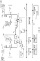
- FIGs. 1 and 2 outline a high level block diagram of link layer circuitry for both transmit (Tx) and receive (Rx) directions, where a link is subdivided in 4x4 port configuration, and Ports 0 and 2 are annotated to support both cache and memory traffic.
- Tx transmit
- Rx receive
- Ports 0 and 2 are annotated to support both cache and memory traffic.
- ports and links widths are possible in other embodiments.
- FIG. 1 shown is a block diagram of a control circuit that may be present in a link layer in accordance with an embodiment.
- a transmit pipe of a control circuit 100 such as a CXLCM controller is shown.
- This control circuit may be present in link layer circuitry of a CXL protocol stack. While this control circuit is for an embodiment according to a CXL implementation, understand that other implementations are possible.
- incoming information may be received in a given buffer 110, 115. More specifically, incoming cache memory protocol traffic may be stored in cache transmit buffers 110. In turn incoming memory protocol traffic may be stored in memory transmit buffers 115.
- buffers 110, 115 may include or be associated with control circuitry to handle buffer management, e.g., using a credit-based mechanism. With dedicated protocol-based buffers, multi-protocol design may be simplified and various forward progress rules are enforced.
- first selection circuit 120 When a given cache memory data unit, such as a packet, flit or so forth is selected for output from buffer 110, it is provided to a first selection circuit 120, which may be implemented as a swizzle multiplexer. Note that communication of protocol traffic throughout the link layer may be on the basis of CXL network flits. As shown, first selection circuit 120 may direct this cache memory protocol traffic to a selected one of multiple logical ports 130.
- each logical port may be mapped to a corresponding physical port present in a physical circuit (not shown for ease of illustration in FIG. 1 ).
- cache memory protocol traffic may be directed to a selected one of logical port 130o and logical port 130 2 . Of course in other implementations, this traffic may be directed to any of the other logical ports.
- each of these ports also may be configured to receive memory protocol traffic.
- Address decoder 125 in turn may direct a given memory protocol traffic unit to a given one of logical ports 130.
- Address decoder 125 routes CXL.mem protocol messages to any of ports 130 0-3 , depending on which CXL device a memory request message is destined. In this way address decoder 115 routes a memory request transaction in one-master-to-many-subordinates fashion.
- Ports 130 may be defined as logical (and potentially structural) entities that provide one-to-one mapping to a subdivided FxB link (and thus to corresponding physical ports of a physical layer).
- Annotation of (CM) in ports 130o and 130 2 specifies that a given port is capable of packing cache and memory transactions, whereas (M) specifies that a given port is capable of packing memory transactions only (e.g., ports 130i and 130 3 ).
- CM CM
- M specifies that a given port is capable of packing memory transactions only (e.g., ports 130i and 130 3 ).
- embodiments implement a silicon area optimized design where a 'superset' capable port is not required for all port [i] instances.
- each port 130 may output N bytes of data information (e.g., 16 bytes in one example).
- the output of pairs of ports 130 may be provided to an additional level of selection circuits, namely subdivision multiplexers 140, 145.
- up to 2N bytes may be output from these multiplexers to another level selection circuit, namely another subdivision multiplexer 150, which may pass given traffic on particular lanes of a data bus 160.
- the various selection circuits may be implemented below port [i] hierarchies.
- Data bus 160 may be implemented as a LPIF data bus to couple a link layer to a physical layer circuit, that in turn couples to one or more devices via a CXL link. Understand while shown at this high level in the embodiment of FIG. 1 , many variations and alternatives are possible.
- FIG. 2 shown is a block diagram of a control circuit that may be present in a link layer in accordance with another embodiment.
- a receive pipe of a control circuit 200 such as a CXLCM controller is shown.
- This control circuit may be present in link layer circuitry of a CXL protocol stack (and may be included as part of the same circuitry as control circuit of FIG. 1 ).
- incoming information e.g., from a data bus 260 is received via physical layer circuitry and provided via selection circuitry implemented as a subdivision demultiplexer 250 and to an additional level of selection circuits, namely subdivision demultiplexers 240, 245.
- selection circuitry implemented as a subdivision demultiplexer 250 and to an additional level of selection circuits, namely subdivision demultiplexers 240, 245.
- up to 2N bytes that are received may be output in N byte chunks to corresponding logical ports 230 0 -230 3 , each of which may be mapped to a corresponding physical port present in a physical circuit.
- logical port 230 0 and logical port 230 2 may communicate via a selection circuit 220, which may be implemented as a swizzle demultiplexer, to a cache receive buffer 210.
- memory protocol traffic may be directed from any of ports 230 0 -230 n to a memory receive buffer 215. Understand while shown at this high level in the embodiment of FIG. 2 , many variations
- Selection circuitry present in control circuits 100 and 200 may be used to route concurrent cache and memory traffic to various sub-divided ports through a controller stack. Depending on implementation, selection control for this circuitry may be performed on a hardware autonomous or software basis.
- a link layer may use information presented on a LPIF control interface bus to determine whether to activate particular select lines.
- physical layer (pl_protocol) encodings according to a LPIF definition provide clues about device types that are detected during training. Details about such 3-bit encodings are available in the LPIF specification and attached devices advertise protocol encodings during boot-time that it intends to be operational during run-time.
- This hardware autonomous approach may enable a CXLCM controller to sample and latch p1_protocol encodings and implement a phased priority approach to activate selection circuitry.
- Table 1 illustrates a possible approach; however an alternate implementation may choose not to follow this behavior.
- Protocol encodings may be only be forwarded to a CXLCM controller once a concrete personality of device attached has been established. This means that protocol encodings on per-port basis may show up in different timestamps.
- a hardware implementation may choose to gate virtual link state training for all ports until protocol encodings associated with all ports are received. Alternatively, hardware may choose to train ports that have received pertinent protocol encodings and rely on logging user-defined severity errors if more than one cache-capable device shows up.
- method 300 is a method for booting up a system having a CXL link to which devices may couple.
- Method 300 may be performed on boot up and may be implemented within a logical portion of a physical circuit, e.g., executed as part of link training. As such method 300 may be performed by hardware circuitry alone, or combination with firmware and/or software.
- method 300 begins by performing link training between link partners, which may include discovery of devices coupled to the link (block 310). By way of this link training, devices coupled to the CXL link can be identified as well as their communication capabilities.
- this information it may be determined, on a per port basis, what type of communication protocol is detected with regard to a device coupled to such port (block 320). For example, in an implementation in which a physical circuit includes 4 physical ports, up to 4 devices may be coupled, each to one of these ports. Different manners of detecting the device types can occur in different implementations. In some cases, devices may communicate, on boot up, certain initialization information that includes an identification of the type of device. Of course this information can be discovered in other manners, such as via boot time information, e.g., provided by a basic input output system (BIOS) or other system software.
- BIOS basic input output system
- this message may be implemented as pl_protocol message.
- this message may be sent, on a per port basis, to a controller of a link layer to which the physical circuit is coupled. Understand that with this information regarding the detected protocols, the link layer in turn may configure its internal circuitry to pass data of the appropriate protocol type via its internal logical ports.
- method 400 is a method for booting up a system having a CXL link, and more particularly to operations performed within a link layer circuit. As such method 400 may be performed by hardware circuitry alone, or combination with firmware and/or software.
- method 400 begins by receiving a physical layer protocol message from physical layer (block 410).
- this message which in a CXL implementation having a LPIF data bus to interconnect link layer and physical layer, can be a pl_protocol message, may be received on a per port basis.
- at least one selection circuit may be configured based on this message information. For example, with reference back to FIG. 1 , first selection circuit 120 may be configured based on such physical layer protocol messages.
- link training may be performed based on the configuration of the link layer. More specifically, this training may be used to ensure that communication between devices occurs with appropriate parameters to ensure a low error rate. As part of this training, a virtual link state machine training may occur to thus place the link into active state.
- messages may be communicated from the link layer and through the physical layer to a given device.
- CXL. cache and CXL.memory protocol traffic may be directed on a selected one of multiple ports, thus providing greater flexibility within a system. Understand while shown at this high level in the embodiment of FIG. 4 , many variations and alternatives are possible.
- system software such as BIOS, which is used to enumerate, setup, and configure CXL stacks to operate under various topological and platform constraints, can be used to control selection lines once during boot, to scatter CXL.cache traffic to a selected port to perform flit packing.
- this technique can be used to control selection lines once during boot to gather CXL.cache traffic from a selected port after flit unpacking.
- hardware can explicitly be programmed to enter link-active state once selection lines are appropriately configured in tandem.
- method 500 is another method for booting up a system having a CXL link, and more particularly to operations performed within a link layer circuit. As such method 500 may be performed by hardware circuitry alone, or combination with firmware and/or software.
- method 500 begins by receiving configuration message, on a per port basis, from system software (block 510).
- this message may be from BIOS and may include flexible topology control information including configuration bits that can be used to set fields in one or more configuration registers.
- at least one selection circuit e.g., , first selection circuit 120 of FIG. 1
- this configuration information may be configured based on this configuration information.
- link training may be performed based on the configuration of the link layer, including virtual link state machine training to place the link into active state.
- messages may be communicated from the link layer and through the physical layer to a given device.
- CXL.cache and CXL.memory protocol traffic may be directed on a selected one of multiple ports, thus providing greater flexibility within a system.
- this software control can be according to BIOS controllable register bits, which may be stored in a configuration register that may be present within a CXLCM controller.
- a first configuration bit may be implemented as a first indicator, referred to as swizzle_active, which can be used to control swizzling CXL.cache traffic to/from Port 0.
- This indicator may be set when CXL.cache traffic is to be routed to/from a logical Port 2 hierarchy when BIOS discovers that a cache-capable Type 1 or Type 2 device is attached to Port 2.
- This indicator may not be written if a cache-capable Type 1 or Type 2 device is attached to Port 0.
- this bit-field may be implemented using a 'lock' attribute such that its contents are not allowed to be accidentally modified once a go_train indicator (defined next) is programmed.
- a second configuration bit may be implemented as a second indicator, referred to as go_train, which can be used to control a CXLCM controller requesting to enter into a link active state and provide a guarantee that the swizzle_active bit is programmed with the desired value.
- this bit-field is implemented using a 'write-to-set' attribute such that its contents can only be written to a value of 0x1 and not allowed to be accidentally overwritten (cleared) once set. Once this bit-field is written into, it may be used to lock the swizzle_active bit indication to preserve intended hardware behavior.
- Table 2 FLEX_ TOPO_CTRL Bit Width Bit Offset Field Name Access Type Default Description 1 0 swizzle_active RW/L 0x0
- This bit controls swizzling traffic. When set, CXL. cache traffic on Logical Port 0 traffic will be routed to/from Physical Port 2 and vice-versa.
- This bit has Lock attribute which means Lockable for that register field contingent to programming of go_train bit 1 1 go_train RW/1S 0x0 Go indication for IP's virtual Link State Machines to request for Active. This is an additional requirement that must be evaluated in conjunction to LPIF control signals. Software must only write to this bit once desired configuration for swizzle_active has been programmed. set-on-write attribute will ensure that once register is written, S/W will not be able to accidentally reprogram it to 0.
- interface circuit 600 is for interfacing a given device such as a transmitter and/or receiver to a link.
- interface circuit 600 is a CXL interface circuit.
- CXL interface circuit 600 includes a transaction layer 610, a link layer 620, and a physical layer 640.
- CXL transaction layer 610 various components are included to enable transaction layer processing for PCIe/CXL.io communications and CXL.cache and CXL.memory transactions.
- a PCIe/CXL.io transaction layer 1015 includes a control circuit 612, which may perform various transaction layer control operations.
- transaction layer 610 further includes a PCIe transaction layer 616 and additional circuitry 618 for handling enhancements to PCIe transaction layer 616 for handling CXL.io transactions.
- CXL.cache and CXL.memory transaction layer 619 may perform transaction layer processing for these protocols.
- a PCIe/CXL.io link layer 625 includes a PCIe data link layer 626 and additional circuitry 628 for handling enhancements to PCIe data link layer 626 for handling CXL.io transactions.
- CXL.cache and CXL.memory link layer 629 may perform link layer processing for these protocols using a single logic stack without logic duplication. As described herein, such processing includes flexibly routing CXL.cache and CXL.mem protocol traffic on selected logical ports.
- a control circuit 622 may configure selection circuitry within link layer 629 to direct given protocol traffic to particular logical ports.
- control circuit 622 may include or be coupled to one or more configuration registers 627. Such configuration registers may include one or more fields to control the selection circuitry as described herein.
- link layer 620 is coupled to an arbiter/multiplexer 1030 that is to receive incoming data streams from link layer 620 and select a data stream (or portion thereof) for communication to a physical layer 640.
- physical layer 640 may be a physical layer to further process incoming data packets for communication on a physical link, which in an embodiment may be a flex bus.
- physical layer 640 includes a PCIe/CXL logical circuit 642 and a PCIe/CXL electrical circuit 646. As seen, these circuits include respective control circuits 645, 648 to control processing within physical layer 640. With embodiments herein, control circuit 645 may send pl_protocol messages to link layer 620 to indicate detection of particular device types on a CXL link. After all such processing is completed, outgoing transaction layer data packets may be communicated on the link. Similarly, incoming transaction layer data packets may be received within physical layer 640 and processed within the communication stack of interface circuit 600. Understand while shown at this high level in the embodiment of FIG. 6 , many variations and alternatives are possible.
- FIG. 7 is a block diagram of a system in accordance with an embodiment.
- a device 705 may be an accelerator or processor device coupled to a host processor 745 via an interconnect 789, which may be single interconnect, bus, trace, and so forth.
- Device 705 and host processor 745 may communicate over link 789 to enable data and messages to pass therebetween.
- link 789 may be operable to support multiple protocols and communication of data and messages via the multiple interconnect protocols, including a CXL protocol as described herein.
- link 789 may support various interconnect protocols, including a non-coherent interconnect protocol, a coherent interconnect protocol, and a memory interconnect protocol.
- Non-limiting examples of supported interconnect protocols may include PCI, PCIe, USB, IDI, IOSF, SMI, SMI3, SATA, CXL.io, CXL.cache, and CXL.mem, and/or the like.
- device 705 may include accelerator logic 725 including circuitry 729.
- accelerator logic 725 and circuitry 729 may provide processing and memory capabilities.
- Examples of device 705 may include producer-consumer devices such as a graphics or other specialized accelerator, producer-consumer plus devices, software-assisted device memory devices, autonomous device memory devices, and giant cache devices.
- accelerator logic 725 may couple to an optional accelerator memory 730.
- Accelerator logic 725 and circuitry 729 may provide the processing and memory capabilities based on the device.
- accelerator logic 725 and circuitry 729 may communicate using, for example, a coherent interconnect protocol for various functions, such as coherent requests and memory flows with host processor 745 via interface logic 713 and circuitry 727.
- Interface logic 713 and circuitry 727 may determine an interconnect protocol based on the messages and data for communication. Understand that with embodiments herein, circuitry 727 may include selection circuitry to direct, e.g., CXL.cache and CXL.memory protocol traffic, via a selected one of multiple logical ports as described herein. In some embodiments, interface logic 713 may be coupled to a multi-protocol multiplexer 710 having one or more protocol queues 712 to send and receive messages and data with host processor 745. Protocol queue 712 may be protocol specific such that each interconnect protocol may be associated with a particular protocol queue. Multiplexer 710 may also implement arbitration circuitry to arbitrate between communications of different protocols and provide selected communications to a physical layer 715.
- host processor 745 may be a main processor such as a CPU.
- Host processor 745 may be coupled to a host memory 740 and may include coherence logic (or coherence and cache logic) 755, which may include a cache hierarchy.
- Coherence logic 755 may communicate using various interconnects with interface logic 7763 including circuitry 761 and one or more cores 765a-n. In some embodiments, coherence logic 755 may enable communication via one or more of a coherent interconnect protocol and a memory interconnect protocol.
- host processor 740 may include a device 770 to communicate with a bus logic 760 over an interconnect.
- device 770 may be an I/O device, such as a PCIe I/O device.
- one or more external devices such as PCIe devices may couple to bus logic 770.
- host processor 745 may include interface logic 763 and circuitry 761 to enable multi-protocol communication between the components of host processor 745 and device 705.
- Interface logic 763 and circuitry 761 may process and enable communication of messages and data between host processor 745 and device 705 in accordance with one or more interconnect protocols, e.g., a non-coherent interconnect protocol, a coherent interconnect, protocol, and a memory interconnect protocol, dynamically.
- interface logic 763 and circuitry 761 may determine a message type for each message and determine which interconnect protocol of a plurality of interconnect protocols to process each of the messages. Different interconnect protocols may be utilized to process the messages.
- circuitry 1161 may include selection circuitry to direct, e.g., CXL.cache and CXL.memory protocol traffic via a selected one of multiple logical ports as described herein.
- interface logic 763 may be coupled to a multi-protocol multiplexer 750 having one or more protocol queues 752 to send and receive messages and data with device 705.
- Protocol queue 752 may be protocol specific such that each interconnect protocol may be associated with a particular protocol queue.
- Multiplexer 750 may also implement arbitration circuitry to arbitrate between communications of different protocols and provide selected communications to a physical layer 754.
- a system 800 may be any type of computing device, and in one embodiment may be a server system such as an edge platform.
- system 800 includes multiple CPUs 810a,b that in turn couple to respective system memories 820a,b which in embodiments may be implemented as double data rate (DDR) memory.
- DDR double data rate
- CPUs 810 may couple together via an interconnect system 815 such as an Intel ® Ultra Path Interconnect or other processor interconnect technology.
- each interconnect 830 may be a given instance of a CXL.
- respective CPUs 810 couple to corresponding field programmable gate arrays (FPGAs)/accelerator devices 850a,b (which may include graphics processing units (GPUs), in one embodiment.
- FPGAs field programmable gate arrays
- GPUs graphics processing units
- CPUs 810 also couple to smart network interface circuit (NIC) devices 860a,b.
- NIC devices 860a,b couple to switches 880a,b (e.g., CXL switches in accordance with an embodiment) that in turn couple to a pooled memory 890a,b such as a persistent memory.
- switches 880a,b e.g., CXL switches in accordance with an embodiment
- CPUs 810 may direct information of multiple communication protocols (e.g., CXL.cache and CXL.memory protocol traffic) via a selected one of multiple logical ports as described herein to devices 850 on a flexibly allocated port of a CXL link. As shown information can be stored in a pooled memory 890. In turn, CPUs 810 or other entities may access and further process this information from pooled memory 890.
- multiple communication protocols e.g., CXL.cache and CXL.memory protocol traffic
- SoC 900 may be configured for insertion in any type of computing device, ranging from portable device to server system.
- SoC 900 includes 2 cores 906 and 907.
- Cores 906 and 907 may conform to an Instruction Set Architecture, such as an Intel ® Architecture Core TM -based processor, an Advanced Micro Devices, Inc. (AMD) processor, a MIPS-based processor, an ARM-based processor design, or a customer thereof, as well as their licensees or adopters.
- AMD Advanced Micro Devices, Inc.
- MIPS Micro Devices, Inc.
- ARM-based processor design or a customer thereof, as well as their licensees or adopters.
- Cores 906 and 907 are coupled to cache controller 908 that is associated with bus interface unit 909 and L2 cache 910 to communicate with other parts of system 900 via an interconnect 912, which in an embodiment may provide for communication according to multiple protocols including CXL.cache and CXL.memory protocol traffic via a selected one of multiple logical ports as described herein.
- bus interface unit 909 includes a DMA circuit 911 configured to send write requests.
- Interconnect 912 provides communication channels to the other components, such as a Subscriber Identity Module (SIM) 930 to interface with a SIM card, a boot ROM 935 to hold boot code for execution by cores 906 and 907 to initialize and boot SoC 900, a SDRAM controller 940 to interface with external memory (e.g., DRAM 960), a flash controller 945 to interface with non-volatile memory (e.g., flash 965), a peripheral controller 950 (e.g., an eSPI interface) to interface with peripherals, video codec 920 and video interface 925 to display and receive input (e.g., touch enabled input), GPU 915 to perform graphics related computations, etc.
- SIM Subscriber Identity Module
- boot ROM 935 to hold boot code for execution by cores 906 and 907 to initialize and boot SoC 900
- SDRAM controller 940 to interface with external memory (e.g., DRAM 960)
- flash controller 945 to interface with non-volatile memory (e.g
- system 900 may additionally include interfaces including a MIPI interface 992, e.g., to a display and/or an HDMI interface 995 also which may couple to the same or a different display.
- MIPI interface 992 e.g., to a display
- HDMI interface 995 also which may couple to the same or a different display.
- multiprocessor system 1000 includes a first processor 1070 and a second processor 1080 coupled via a point-to-point interconnect 1050.
- processors 1070 and 1080 may be many core processors including representative first and second processor cores (i.e., processor cores 1074a and 1074b and processor cores 1084a and 1084b).
- processors 1070 and 1080 further include point-to point interconnects 1077 and 1087, which couple via interconnects 1042 and 1044 (which may be CXL buses) to switches 1059 and 1060.
- interconnects 1042 and 1044 which may be CXL buses
- Such traffic may be according to multiple protocols, including CXL.cache and CXL.memory protocol traffic via a selected one of multiple logical ports as described herein.
- switches 1059, 1060 couple to pooled memories 1055 and 1065.
- first processor 1070 further includes a memory controller hub (MCH) 1072 and point-to-point (P-P) interfaces 1076 and 1078.
- second processor 1080 includes a MCH 1082 and P-P interfaces 1086 and 1088.
- MCH's 1072 and 1082 couple the processors to respective memories, namely a memory 1032 and a memory 1034, which may be portions of system memory (e.g., DRAM) locally attached to the respective processors.
- First processor 1070 and second processor 1080 may be coupled to a chipset 1090 via P-P interconnects 1076 and 1086, respectively.
- chipset 1090 includes P-P interfaces 1094 and 1098.
- chipset 1090 includes an interface 1092 to couple chipset 1090 with a high performance graphics engine 1038, by a P-P interconnect 1039.
- various input/output (I/O) devices 1014 may be coupled to first bus 1016, along with a bus bridge 1018 which couples first bus 1016 to a second bus 1020.
- Various devices may be coupled to second bus 1020 including, for example, a keyboard/mouse 1022, communication devices 1026 and a data storage unit 1028 such as a disk drive or other mass storage device which may include code 1030, in one embodiment.
- an audio I/O 824 may be coupled to second bus 1020.
- Embodiments as described herein can be used in a wide variety of network architectures. To this end, many different types of computing platforms in a networked architecture that couples between a given edge device and a datacenter can perform the fine-grained monitoring and tracing described herein.
- FIG. 11 shown is a block diagram of a network architecture in accordance with another embodiment of the present invention. As shown in FIG. 11 , network architecture 1100 includes various computing platforms that may be located in a very wide area, and which have different latencies in communicating with different devices.
- network architecture 1100 includes a representative device 1110, such as a smartphone. This device may communicate via different radio access networks (RANs), including a RAN 1120 and a RAN 1130. RAN 1120 in turn may couple to a platform 1125, which may be an edge platform such as a fog/far/near edge platform, and which may leverage embodiments herein. Other requests may be handled by a far edge platform 1135 coupled to RAN 1130, which also may leverage embodiments.
- RANs radio access networks
- platform 1125 which may be an edge platform such as a fog/far/near edge platform, and which may leverage embodiments herein.
- Other requests may be handled by a far edge platform 1135 coupled to RAN 1130, which also may leverage embodiments.
- another near edge platform 1140 may couple to RANs 1120, 1130.
- this near edge platform may be located closer to a data center 1150, which may have a large amount of computing resources.
- a data center 1150 which may have a large amount of computing resources.
- CXL.cache and CXL.memory protocol traffic via a selected one of multiple logical ports as described herein.
- an apparatus includes: a transaction layer circuit to output transaction layer information; and a link layer circuit coupled to the transaction layer circuit, the link layer circuit to receive and process the transaction layer information and to output link layer information to a physical circuit.
- the link layer circuit may include a first selection circuit to receive and direct cache memory protocol traffic to a selected one of a first logical port and a second logical port.
- the apparatus further comprises a control circuit coupled to the first selection circuit, the control circuit to control the first selection circuit to direct the cache memory protocol traffic to the second logical port, the second logical port mapped to a second physical port of the physical circuit.
- control circuit comprises: a first buffer to store the cache memory protocol traffic; and a second buffer to store memory protocol traffic.
- the first selection circuit is coupled to the first buffer, the first selection circuit to direct the cache memory protocol traffic to a selected one of the first logical port or the second logical port according to control information from the control circuit.
- the apparatus further comprises an address decoder coupled to the second buffer, the address decoder to direct the memory protocol traffic to at least one of the first logical port, the second logical port, a third logical port, and a fourth logical port.
- the apparatus further comprises: a second selection circuit coupled to the first logical port and a third logical port and to direct the cache memory protocol traffic and memory protocol traffic to another selection circuit; and a third selection circuit coupled to the second logical port and a fourth logical port and to direct the cache memory protocol traffic and the memory protocol traffic to the another selection circuit.
- the apparatus further comprises the another selection circuit coupled to the second selection circuit and the third selection circuit.
- the apparatus further comprises at least one configuration register having a first field to store a first indicator, which when a first value is to cause the first selection circuit to direct the cache memory protocol traffic to the second logical port and a second field to store a second indicator which, when set, is to prevent an update to the first indicator.
- control circuit is to receive a configuration message based on a protocol encoding received from the physical circuit, the protocol encoding based on detection of a type of device coupled to the second physical port of the physical circuit.
- control circuit is to cause the first selection circuit to direct the cache memory protocol traffic to the second logical port when a CXL Type 2 device is coupled to the second physical port of the physical circuit.
- a method includes: receiving configuration information regarding connection of a cache-capable device to a first port of a plurality of ports of a physical circuit coupled to the cache-capable device via a data bus; in response to the configuration information, configuring a first selection circuit of a link layer coupled to the physical circuit to cause cache memory protocol traffic to be directed to a first logical port of the link layer mapped to the first port of the physical circuit; and directing the cache memory protocol traffic, via the first selection circuit, to the first logical port and thereafter to the first port of the physical circuit for transfer to the cache-capable device.
- the method further comprises receiving the configuration information comprising one or more protocol encoding messages from the physical circuit, to indicate detection of one or more devices coupled to the plurality of ports of the physical circuit.
- the method further comprises receiving the configuration information comprising a first indicator to indicate that the cache-capable device is coupled to the first port of the physical circuit.
- the method further comprises directing memory protocol traffic, via an address decoder, to a second logical port of the link layer and thereafter to a second port of the plurality of ports of the physical circuit for transfer to a memory device coupled to the second port.
- a computer readable medium including instructions is to perform the method of any of the above examples.
- a computer readable medium including data is to be used by at least one machine to fabricate at least one integrated circuit to perform the method of any one of the above examples.
- an apparatus comprises means for performing the method of any one of the above examples.
- a system includes: a host processor comprising one or more cores and a CXL interface circuit; a cache-capable device coupled to the host processor via a CXL link, the cache-capable device coupled to a second physical port, the second physical port mapped to a second logical port; and a memory device coupled to the host processor via the CXL link, the memory device coupled to a first physical port, the first physical port mapped to a first logical port.
- the CXL interface circuit may include: a transaction layer circuit to output transaction layer information; a link layer circuit coupled to the transaction layer circuit, the link layer circuit to receive and process the transaction layer information and to output link layer information to a physical circuit.
- the link layer circuit may include: a first selection circuit to receive and direct CXL.cache protocol traffic to a selected one of a first logical port and a second logical port; and a plurality of logical ports comprising the first logical port, the second logical port, a third logical port and a fourth logical port, where the first selection circuit is coupled to the first logical port and the second logical port.
- the CXL interface circuit further may include a physical layer circuit coupled to the link layer circuit, the physical layer circuit comprising a logical circuit and a physical circuit, the physical circuit comprising a plurality of physical ports comprising a first physical port, a second physical port, a third physical port and a fourth physical port.
- the link layer circuit comprises a control circuit coupled to the first selection circuit, the control circuit to control the first selection circuit to direct the CXL.cache protocol traffic to the second logical port.
- control circuit comprises: a first buffer to store the CXL.cache protocol traffic; and a second buffer to store CXL.memory protocol traffic.
- the first selection circuit is coupled to the first buffer, the first selection circuit to direct the CXL.cache protocol traffic to the second logical port according to control information from the control circuit.
- control circuit is to generate the control information in response to a protocol encoding from the physical layer circuit, the protocol encoding to indicate detection of the cache-capable device coupled to the second physical port.
- control circuit is to further disable cache functionality of the cache-capable device when another cache-capable device is coupled to the first physical port, the first physical port advertised as Port 0.
- circuit and “circuitry” are used interchangeably herein.
- logic are used to refer to alone or in any combination, analog circuitry, digital circuitry, hard wired circuitry, programmable circuitry, processor circuitry, microcontroller circuitry, hardware logic circuitry, state machine circuitry and/or any other type of physical hardware component.
- Embodiments may be used in many different types of systems. For example, in one embodiment a communication device can be arranged to perform the various methods and techniques described herein.
- the scope of the present invention is not limited to a communication device, and instead other embodiments can be directed to other types of apparatus for processing instructions, or one or more machine readable media including instructions that in response to being executed on a computing device, cause the device to carry out one or more of the methods and techniques described herein.
- Embodiments may be implemented in code and may be stored on a non-transitory storage medium having stored thereon instructions which can be used to program a system to perform the instructions. Embodiments also may be implemented in data and may be stored on a non-transitory storage medium, which if used by at least one machine, causes the at least one machine to fabricate at least one integrated circuit to perform one or more operations. Still further embodiments may be implemented in a computer readable storage medium including information that, when manufactured into a SoC or other processor, is to configure the SoC or other processor to perform one or more operations.
- the storage medium may include, but is not limited to, any type of disk including floppy disks, optical disks, solid state drives (SSDs), compact disk read-only memories (CD-ROMs), compact disk rewritables (CD-RWs), and magneto-optical disks, semiconductor devices such as read-only memories (ROMs), random access memories (RAMs) such as dynamic random access memories (DRAMs), static random access memories (SRAMs), erasable programmable read-only memories (EPROMs), flash memories, electrically erasable programmable read-only memories (EEPROMs), magnetic or optical cards, or any other type of media suitable for storing electronic instructions.
- ROMs read-only memories
- RAMs random access memories
- DRAMs dynamic random access memories
- SRAMs static random access memories
- EPROMs erasable programmable read-only memories
- EEPROMs electrically erasable programmable read-only memories
- magnetic or optical cards or any other type of media suitable for storing electronic instructions.
Abstract
Description
- Embodiments relate to multi-protocol communications via a link.
- Compute Express Link (CXL) is an interconnect technology that allows attachment of CXL-compliant devices to host processor systems. CXL links are implemented according to a given CXL specification such as the CXL Specification version 1.1 (published June 2019). A device may couple to such CXL links via a FlexBus (FxB) port. There may be single or multiple devices attached on the same FxB port concurrently using link subdivision. However currently there are restrictions as to types of devices allowed to be connected to specific lanes of the link, which unduly limits flexibility.
-
-
FIG. 1 is a block diagram of a control circuit that may be present in a link layer in accordance with an embodiment. -
FIG. 2 is a block diagram of a control circuit that may be present in a link layer in accordance with another embodiment. -
FIG. 3 is a flow diagram of a method in accordance with an embodiment. -
FIG. 4 is a flow diagram of a method in accordance with another embodiment. -
FIG. 5 is a flow diagram of a method in accordance with a still further embodiment. -
FIG. 6 is a block diagram of an interface circuit in accordance with an embodiment. -
FIG. 7 is a block diagram of a system in accordance with an embodiment. -
FIG. 8 is a block diagram of a system in accordance with another embodiment of the present invention. -
FIG. 9 is a block diagram of an embodiment of a SoC design in accordance with an embodiment. -
FIG. 10 is a block diagram of a system in accordance with another embodiment of the present invention. -
FIG. 11 is a block diagram of a network architecture in accordance with an embodiment. - In various embodiments, a data link layer (also "link layer" or "link layer circuit" herein) is provided that can support multi-protocol message transmission and further allow flexibility as to device types that may be attached on specific lanes of an interconnect. As a result, richer feature sets can be realized without an added cost in terms of silicon area and power.
- This data link layer may be part of a protocol stack through which communications flow, where the protocol stack further includes a transaction layer and a physical layer. While flexible device attachment and link layer circuitry are described in connection with a CXL-based system, embodiments are not limited in this regard.
- Further while one example use case is for a cloud-based architecture that may communicate using interconnects and switches in accordance with a CXL specification such as the CXL 1.1 Specification or any future versions, modifications, variations or alternatives, other implementations are possible. For example embodiments may be used in other coherent interconnect technologies such as an IBM XBus protocol, an Nvidia NVLink protocol, an AMD Infinity Fabric protocol, cache coherent interconnect for accelerators (CCIX) protocol or coherent accelerator processor interface (OpenCAPI).
- In a CXL implementation, traffic flows of different communication protocols are sent along CXL interconnects. For example, there may be separate traffic flows including so-called CXL.cache, CXL.io and CXL.mem communication protocols via which traffic of different communication protocols is communicated. More generally, the interconnect may support various interconnect protocols, including a non-coherent interconnect protocol, a coherent interconnect protocol, and a memory interconnect protocol. Non-limiting examples of supported interconnect protocols may include PCI, PCIe, USB, IDI, IOSF, SMI, SMI3, SATA, CXL.io, CXL.cache, and CXL.mem, and/or the like.
- With embodiments a microarchitecture for a data link layer may include circuitry to flexibly support multiple protocols (such as both CXL.cache and CXL.mem (collectively here "CXL.cache-mem") through a single pipeline, where protocol traffic is routed to apropos bifurcated physical lanes without adding extra performance overheads and hardware penalties.
- In different implementations, configuration of a link layer to provide flexible port mappings can be realized using hardware autonomous techniques that may ameliorate any system software overhead, or using a software-based technique via system level software. With embodiments herein, platform architects and users can realize flexible attach points for CXL
Type 1 and 2 (cache-capable) devices without additional hardware cost. That is, link layer and other circuitry may be reused across ports instead of duplicating data main-band modules for packing communications. As such, embodiments provide flexibility with negligible power, performance, and area impact. - With embodiments, common design resources are used to realize link subdivision without logic replication, thus providing flexibility with negligible power and area impact, and no performance impact. For instance, embodiments use shared buffer resources for CXL.cache protocol traffic across ports and use multiplexing and demultiplexing schemes to route traffic to apropos device/port, realizing significant reduction of bit-cells for storage.
- Embodiments also operate with zero performance degradation both in terms of latency and bandwidth, by simplifying selection circuitry to be a single logic level scheme and restricting bus routing requirements for CXL.cache channel only. Other link specific peripheral functions built into the controller such as RAS, power management may continue to operate on per-port granularity, seamlessly. Other unique host specific implementation functions built into the controller such as bus lock and interrupt handling may also operate seamlessly and need not be made aware of Flexbus topology.
- In embodiments a link layer may include a personality agnostic data link layer (CXLCM) module as a controller instance (referred to herein as a "CXLCM controller") capable of transporting CXL.cache and CXL.mem protocol messages over a FxB link without any restrictions on where a cache-capable device is attached. In some cases any port may be selected as an attach point for a cache-capable device. According to current CXL architectural requirements, a cache-
capable Type 1 orType 2 device warrants support for x8 link width. To reduce routing requirements, an embodiment may enable selection of a limited number of ports as a choice of attach point for connecting an accelerator to CPU host. Of course embodiments are not limited in this regard, and other embodiments may extend support to all ports where support for x4 cache-capable devices is warranted. - In an embodiment, the CXLCM controller may interface with a logical physical unit (PHY) module according to a data bus in accordance with a Logical PHY Interface (LPIF) Specification, such as the LPIF Specification version 1.0 (March 2019) or any future versions, modifications or variations. To enable CXCLM controller configuration, embodiments may use LPIF-based information/encodings to identify detected devices. In an embodiment, a LPIF data bus interface is 16 lanes wide [15:0] and is shared across subdivided ports based on how a FxB link is natively subdivided. For example, for 2x8 attachments, lower 8 lanes [7:0] map to
Port 0 and upper 8 lanes [15:8] map toPort 2 respectively. Similarly, for 4 x4 devices, lanes [3:0], [7:4], [11:8], and [15:12] map toPort 0,Port 1,Port 2, andPort 3, respectively. - With this in perspective,
FIGs. 1 and2 outline a high level block diagram of link layer circuitry for both transmit (Tx) and receive (Rx) directions, where a link is subdivided in 4x4 port configuration, andPorts - Referring now to
FIG. 1 , shown is a block diagram of a control circuit that may be present in a link layer in accordance with an embodiment. As shown inFIG. 1 , a transmit pipe of acontrol circuit 100 such as a CXLCM controller is shown. This control circuit may be present in link layer circuitry of a CXL protocol stack. While this control circuit is for an embodiment according to a CXL implementation, understand that other implementations are possible. - As illustrated, incoming information, e.g., from a transaction layer, may be received in a given
buffer cache transmit buffers 110. In turn incoming memory protocol traffic may be stored inmemory transmit buffers 115. Note thatbuffers - When a given cache memory data unit, such as a packet, flit or so forth is selected for output from
buffer 110, it is provided to afirst selection circuit 120, which may be implemented as a swizzle multiplexer. Note that communication of protocol traffic throughout the link layer may be on the basis of CXL network flits. As shown,first selection circuit 120 may direct this cache memory protocol traffic to a selected one of multiple logical ports 130. - Specifically as shown, in this example there are four logical ports 1300-1303. Each logical port may be mapped to a corresponding physical port present in a physical circuit (not shown for ease of illustration in
FIG. 1 ). With embodiments herein, cache memory protocol traffic may be directed to a selected one of logical port 130o and logical port 1302. Of course in other implementations, this traffic may be directed to any of the other logical ports. - Also, depending upon particular configuration each of these ports also may be configured to receive memory protocol traffic.
Address decoder 125 in turn may direct a given memory protocol traffic unit to a given one of logical ports 130.Address decoder 125 routes CXL.mem protocol messages to any of ports 1300-3, depending on which CXL device a memory request message is destined. In thisway address decoder 115 routes a memory request transaction in one-master-to-many-subordinates fashion. - Ports 130 may be defined as logical (and potentially structural) entities that provide one-to-one mapping to a subdivided FxB link (and thus to corresponding physical ports of a physical layer). Annotation of (CM) in ports 130o and 1302 specifies that a given port is capable of packing cache and memory transactions, whereas (M) specifies that a given port is capable of packing memory transactions only (e.g., ports 130i and 1303). In this way, embodiments implement a silicon area optimized design where a 'superset' capable port is not required for all port [i] instances.
- In an example each port 130 may output N bytes of data information (e.g., 16 bytes in one example). As further illustrated, the output of pairs of ports 130 may be provided to an additional level of selection circuits, namely
subdivision multiplexers subdivision multiplexer 150, which may pass given traffic on particular lanes of adata bus 160. Note that in another embodiment, the various selection circuits may be implemented below port [i] hierarchies.Data bus 160 may be implemented as a LPIF data bus to couple a link layer to a physical layer circuit, that in turn couples to one or more devices via a CXL link. Understand while shown at this high level in the embodiment ofFIG. 1 , many variations and alternatives are possible. - Referring now to
FIG. 2 , shown is a block diagram of a control circuit that may be present in a link layer in accordance with another embodiment. As shown inFIG. 2 , a receive pipe of acontrol circuit 200 such as a CXLCM controller is shown. This control circuit may be present in link layer circuitry of a CXL protocol stack (and may be included as part of the same circuitry as control circuit ofFIG. 1 ). - As illustrated, incoming information, e.g., from a
data bus 260 is received via physical layer circuitry and provided via selection circuitry implemented as asubdivision demultiplexer 250 and to an additional level of selection circuits, namelysubdivision demultiplexers selection circuit 220, which may be implemented as a swizzle demultiplexer, to a cache receivebuffer 210. In turn memory protocol traffic may be directed from any of ports 2300-230n to a memory receivebuffer 215. Understand while shown at this high level in the embodiment ofFIG. 2 , many variations and alternatives are possible. - Selection circuitry present in
control circuits 100 and 200 (e.g.,) may be used to route concurrent cache and memory traffic to various sub-divided ports through a controller stack. Depending on implementation, selection control for this circuitry may be performed on a hardware autonomous or software basis. - In a hardware autonomous implementation, a link layer may use information presented on a LPIF control interface bus to determine whether to activate particular select lines. To this effect, physical layer (pl_protocol) encodings according to a LPIF definition provide clues about device types that are detected during training. Details about such 3-bit encodings are available in the LPIF specification and attached devices advertise protocol encodings during boot-time that it intends to be operational during run-time. This hardware autonomous approach may enable a CXLCM controller to sample and latch p1_protocol encodings and implement a phased priority approach to activate selection circuitry.
- Table 1 illustrates a possible approach; however an alternate implementation may choose not to follow this behavior.
-
- i. Sample pl_protocol encodings on per-port basis as defined in the LPIF specification
- ii. If
Port 0 detects Type1/2 Device andPort 2 did not, trainPort 0 and deactivate swizzle. - iii. If
Port 2 detects Type1/2 Device andPort 0 did not, trainPort 2 and activate swizzle. - iv. If both
Port 0 andPort 2 detect Type1/2 Device, disablePort 2 and deactivate swizzle. Rely on system software to disable caching function ofPort 2 connected device. - Protocol encodings may be only be forwarded to a CXLCM controller once a concrete personality of device attached has been established. This means that protocol encodings on per-port basis may show up in different timestamps. A hardware implementation may choose to gate virtual link state training for all ports until protocol encodings associated with all ports are received. Alternatively, hardware may choose to train ports that have received pertinent protocol encodings and rely on logging user-defined severity errors if more than one cache-capable device shows up. It is generally expected that in a CXL implementation according to a CXL specification version 1.1 or 2.0, only one cache-
capable Type 1/Type 2 device is present behind a link, and a CXL.cache capability in all but one of these devices is disabled if there are plurality of such devices attached. However, handling of such cases either through software intervention or through error reporting mechanisms can be implementation specific, and may vary in future CXL specification versions. - Referring now to
FIG. 3 , shown is a flow diagram of a method in accordance with an embodiment. As shown inFIG. 3 ,method 300 is a method for booting up a system having a CXL link to which devices may couple.Method 300 may be performed on boot up and may be implemented within a logical portion of a physical circuit, e.g., executed as part of link training. Assuch method 300 may be performed by hardware circuitry alone, or combination with firmware and/or software. As illustrated,method 300 begins by performing link training between link partners, which may include discovery of devices coupled to the link (block 310). By way of this link training, devices coupled to the CXL link can be identified as well as their communication capabilities. - As part of this information, it may be determined, on a per port basis, what type of communication protocol is detected with regard to a device coupled to such port (block 320). For example, in an implementation in which a physical circuit includes 4 physical ports, up to 4 devices may be coupled, each to one of these ports. Different manners of detecting the device types can occur in different implementations. In some cases, devices may communicate, on boot up, certain initialization information that includes an identification of the type of device. Of course this information can be discovered in other manners, such as via boot time information, e.g., provided by a basic input output system (BIOS) or other system software.
- Still with reference to
FIG. 3 , control next passes to block 330 where the detected protocol may be encoded, on a per core basis, into a physical layer protocol message. In a CXL implementation where physical layer and link layer couple via a LPIF data bus, this message may be implemented as pl_protocol message. Finally, atblock 340 this message may be sent, on a per port basis, to a controller of a link layer to which the physical circuit is coupled. Understand that with this information regarding the detected protocols, the link layer in turn may configure its internal circuitry to pass data of the appropriate protocol type via its internal logical ports. - Referring now to
FIG. 4 , shown is a flow diagram of a method in accordance with another embodiment. As shown inFIG. 4 ,method 400 is a method for booting up a system having a CXL link, and more particularly to operations performed within a link layer circuit. Assuch method 400 may be performed by hardware circuitry alone, or combination with firmware and/or software. - As shown,
method 400 begins by receiving a physical layer protocol message from physical layer (block 410). As discussed above, this message, which in a CXL implementation having a LPIF data bus to interconnect link layer and physical layer, can be a pl_protocol message, may be received on a per port basis. Next atblock 420, at least one selection circuit may be configured based on this message information. For example, with reference back toFIG. 1 ,first selection circuit 120 may be configured based on such physical layer protocol messages. - Still with reference to
FIG. 4 , next atblock 430 link training may be performed based on the configuration of the link layer. More specifically, this training may be used to ensure that communication between devices occurs with appropriate parameters to ensure a low error rate. As part of this training, a virtual link state machine training may occur to thus place the link into active state. When it is determined atdiamond 440 that training has completed, atblock 450 messages may be communicated from the link layer and through the physical layer to a given device. Here in the context of providing configurable subdivision of a bus, CXL. cache and CXL.memory protocol traffic may be directed on a selected one of multiple ports, thus providing greater flexibility within a system. Understand while shown at this high level in the embodiment ofFIG. 4 , many variations and alternatives are possible. - In another embodiment, system software such as BIOS, which is used to enumerate, setup, and configure CXL stacks to operate under various topological and platform constraints, can be used to control selection lines once during boot, to scatter CXL.cache traffic to a selected port to perform flit packing. Similarly, this technique can be used to control selection lines once during boot to gather CXL.cache traffic from a selected port after flit unpacking. In order to save power when a given link may not be trained, hardware can explicitly be programmed to enter link-active state once selection lines are appropriately configured in tandem.
- Referring now to
FIG. 5 shown is a flow diagram of a method in accordance with a still further embodiment. As shown inFIG. 5 ,method 500 is another method for booting up a system having a CXL link, and more particularly to operations performed within a link layer circuit. Assuch method 500 may be performed by hardware circuitry alone, or combination with firmware and/or software. - As shown,
method 500 begins by receiving configuration message, on a per port basis, from system software (block 510). As discussed above, this message may be from BIOS and may include flexible topology control information including configuration bits that can be used to set fields in one or more configuration registers. Next atblock 520, at least one selection circuit (e.g., ,first selection circuit 120 ofFIG. 1 ) may be configured based on this configuration information. - Still with reference to
FIG. 5 , next atblock 530 link training may be performed based on the configuration of the link layer, including virtual link state machine training to place the link into active state. When it is determined atdiamond 540 that training has completed, atblock 550 messages may be communicated from the link layer and through the physical layer to a given device. Here in the context of providing configurable subdivision of a bus, CXL.cache and CXL.memory protocol traffic may be directed on a selected one of multiple ports, thus providing greater flexibility within a system. - In an embodiment this software control can be according to BIOS controllable register bits, which may be stored in a configuration register that may be present within a CXLCM controller. In one implementation, a first configuration bit may be implemented as a first indicator, referred to as swizzle_active, which can be used to control swizzling CXL.cache traffic to/from
Port 0. This indicator may be set when CXL.cache traffic is to be routed to/from alogical Port 2 hierarchy when BIOS discovers that a cache-capable Type 1 orType 2 device is attached toPort 2. This indicator may not be written if a cache-capable Type 1 orType 2 device is attached toPort 0. In an embodiment, this bit-field may be implemented using a 'lock' attribute such that its contents are not allowed to be accidentally modified once a go_train indicator (defined next) is programmed. - In one implementation, a second configuration bit may be implemented as a second indicator, referred to as go_train, which can be used to control a CXLCM controller requesting to enter into a link active state and provide a guarantee that the swizzle_active bit is programmed with the desired value. In an embodiment, this bit-field is implemented using a 'write-to-set' attribute such that its contents can only be written to a value of 0x1 and not allowed to be accidentally overwritten (cleared) once set. Once this bit-field is written into, it may be used to lock the swizzle_active bit indication to preserve intended hardware behavior.
- These indicators for a particular embodiment, are further described in Table 2.
Table 2 FLEX_ TOPO_CTRL Bit Width Bit Offset Field Name Access Type Default Description 1 0 swizzle_active RW/L 0x0 This bit controls swizzling traffic. When set, CXL. cache traffic on Logical Port 0 traffic will be routed to/fromPhysical Port 2 and vice-versa. This bit has Lock attribute which means Lockable for that register field contingent to programming ofgo_train bit 1 1 go_train RW/1S 0x0 Go indication for IP's virtual Link State Machines to request for Active. This is an additional requirement that must be evaluated in conjunction to LPIF control signals. Software must only write to this bit once desired configuration for swizzle_active has been programmed. set-on-write attribute will ensure that once register is written, S/W will not be able to accidentally reprogram it to 0. - Referring now to
FIG. 6 , shown is a block diagram of an interface circuit in accordance with an embodiment. More specifically as shown inFIG. 6 ,interface circuit 600 is for interfacing a given device such as a transmitter and/or receiver to a link. In the embodiment shown inFIG. 6 ,interface circuit 600 is a CXL interface circuit. As shown,CXL interface circuit 600 includes atransaction layer 610, alink layer 620, and aphysical layer 640. With reference toCXL transaction layer 610, various components are included to enable transaction layer processing for PCIe/CXL.io communications and CXL.cache and CXL.memory transactions. More particularly, a PCIe/CXL.io transaction layer 1015 includes acontrol circuit 612, which may perform various transaction layer control operations. In addition,transaction layer 610 further includes aPCIe transaction layer 616 andadditional circuitry 618 for handling enhancements toPCIe transaction layer 616 for handling CXL.io transactions. In turn, CXL.cache and CXL.memory transaction layer 619 may perform transaction layer processing for these protocols. - With reference to
CXL link layer 620, various components are included to enable link layer processing for PCIe/CXL.io communications and CXL.cache and CXL.memory transactions. More particularly, a PCIe/CXL.io link layer 625 includes a PCIedata link layer 626 andadditional circuitry 628 for handling enhancements to PCIedata link layer 626 for handling CXL.io transactions. - In turn, CXL.cache and CXL.
memory link layer 629 may perform link layer processing for these protocols using a single logic stack without logic duplication. As described herein, such processing includes flexibly routing CXL.cache and CXL.mem protocol traffic on selected logical ports. To this end, acontrol circuit 622 may configure selection circuitry withinlink layer 629 to direct given protocol traffic to particular logical ports. In an embodiment,control circuit 622 may include or be coupled to one or more configuration registers 627. Such configuration registers may include one or more fields to control the selection circuitry as described herein. - With further reference to
FIG. 6 ,link layer 620 is coupled to an arbiter/multiplexer 1030 that is to receive incoming data streams fromlink layer 620 and select a data stream (or portion thereof) for communication to aphysical layer 640. - In an embodiment,
physical layer 640 may be a physical layer to further process incoming data packets for communication on a physical link, which in an embodiment may be a flex bus. As illustrated,physical layer 640 includes a PCIe/CXLlogical circuit 642 and a PCIe/CXLelectrical circuit 646. As seen, these circuits includerespective control circuits physical layer 640. With embodiments herein,control circuit 645 may send pl_protocol messages to linklayer 620 to indicate detection of particular device types on a CXL link. After all such processing is completed, outgoing transaction layer data packets may be communicated on the link. Similarly, incoming transaction layer data packets may be received withinphysical layer 640 and processed within the communication stack ofinterface circuit 600. Understand while shown at this high level in the embodiment ofFIG. 6 , many variations and alternatives are possible. -
FIG. 7 is a block diagram of a system in accordance with an embodiment. As shown inFIG. 7 adevice 705 may be an accelerator or processor device coupled to ahost processor 745 via aninterconnect 789, which may be single interconnect, bus, trace, and so forth.Device 705 andhost processor 745 may communicate overlink 789 to enable data and messages to pass therebetween. In some embodiments, link 789 may be operable to support multiple protocols and communication of data and messages via the multiple interconnect protocols, including a CXL protocol as described herein. For example, link 789 may support various interconnect protocols, including a non-coherent interconnect protocol, a coherent interconnect protocol, and a memory interconnect protocol. Non-limiting examples of supported interconnect protocols may include PCI, PCIe, USB, IDI, IOSF, SMI, SMI3, SATA, CXL.io, CXL.cache, and CXL.mem, and/or the like. - In embodiments,
device 705 may includeaccelerator logic 725 includingcircuitry 729. In some instances,accelerator logic 725 andcircuitry 729 may provide processing and memory capabilities. Examples ofdevice 705 may include producer-consumer devices such as a graphics or other specialized accelerator, producer-consumer plus devices, software-assisted device memory devices, autonomous device memory devices, and giant cache devices. In some cases,accelerator logic 725 may couple to anoptional accelerator memory 730.Accelerator logic 725 andcircuitry 729 may provide the processing and memory capabilities based on the device. For example,accelerator logic 725 andcircuitry 729 may communicate using, for example, a coherent interconnect protocol for various functions, such as coherent requests and memory flows withhost processor 745 viainterface logic 713 andcircuitry 727. -
Interface logic 713 andcircuitry 727 may determine an interconnect protocol based on the messages and data for communication. Understand that with embodiments herein,circuitry 727 may include selection circuitry to direct, e.g., CXL.cache and CXL.memory protocol traffic, via a selected one of multiple logical ports as described herein. In some embodiments,interface logic 713 may be coupled to amulti-protocol multiplexer 710 having one ormore protocol queues 712 to send and receive messages and data withhost processor 745.Protocol queue 712 may be protocol specific such that each interconnect protocol may be associated with a particular protocol queue.Multiplexer 710 may also implement arbitration circuitry to arbitrate between communications of different protocols and provide selected communications to aphysical layer 715. - In various embodiments,
host processor 745 may be a main processor such as a CPU.Host processor 745 may be coupled to ahost memory 740 and may include coherence logic (or coherence and cache logic) 755, which may include a cache hierarchy.Coherence logic 755 may communicate using various interconnects with interface logic 7763 includingcircuitry 761 and one or more cores 765a-n. In some embodiments,coherence logic 755 may enable communication via one or more of a coherent interconnect protocol and a memory interconnect protocol. - In various embodiments,
host processor 740 may include adevice 770 to communicate with abus logic 760 over an interconnect. In some embodiments,device 770 may be an I/O device, such as a PCIe I/O device. In other cases, one or more external devices such as PCIe devices may couple tobus logic 770. - In embodiments,
host processor 745 may includeinterface logic 763 andcircuitry 761 to enable multi-protocol communication between the components ofhost processor 745 anddevice 705.Interface logic 763 andcircuitry 761 may process and enable communication of messages and data betweenhost processor 745 anddevice 705 in accordance with one or more interconnect protocols, e.g., a non-coherent interconnect protocol, a coherent interconnect, protocol, and a memory interconnect protocol, dynamically. For example,interface logic 763 andcircuitry 761 may determine a message type for each message and determine which interconnect protocol of a plurality of interconnect protocols to process each of the messages. Different interconnect protocols may be utilized to process the messages. In addition, circuitry 1161 may include selection circuitry to direct, e.g., CXL.cache and CXL.memory protocol traffic via a selected one of multiple logical ports as described herein. - In some embodiments,
interface logic 763 may be coupled to amulti-protocol multiplexer 750 having one ormore protocol queues 752 to send and receive messages and data withdevice 705.Protocol queue 752 may be protocol specific such that each interconnect protocol may be associated with a particular protocol queue.Multiplexer 750 may also implement arbitration circuitry to arbitrate between communications of different protocols and provide selected communications to aphysical layer 754. - Referring now to
FIG. 8 , shown is a block diagram of a system in accordance with another embodiment of the present invention. As shown inFIG. 8 , asystem 800 may be any type of computing device, and in one embodiment may be a server system such as an edge platform. In the embodiment ofFIG. 8 ,system 800 includesmultiple CPUs 810a,b that in turn couple torespective system memories 820a,b which in embodiments may be implemented as double data rate (DDR) memory. Note that CPUs 810 may couple together via aninterconnect system 815 such as an Intel® Ultra Path Interconnect or other processor interconnect technology. - To enable coherent accelerator devices and/or smart adapter devices to couple to CPUs 810 by way of potentially multiple communication protocols, a plurality of interconnects 830a1-b2 may be present. In an embodiment, each interconnect 830 may be a given instance of a CXL.
- In the embodiment shown, respective CPUs 810 couple to corresponding field programmable gate arrays (FPGAs)/
accelerator devices 850a,b (which may include graphics processing units (GPUs), in one embodiment. In addition CPUs 810 also couple to smart network interface circuit (NIC)devices 860a,b. In turn,smart NIC devices 860a,b couple toswitches 880a,b (e.g., CXL switches in accordance with an embodiment) that in turn couple to a pooledmemory 890a,b such as a persistent memory. With an arrangement as inFIG. 8 , CPUs 810 may direct information of multiple communication protocols (e.g., CXL.cache and CXL.memory protocol traffic) via a selected one of multiple logical ports as described herein to devices 850 on a flexibly allocated port of a CXL link. As shown information can be stored in a pooled memory 890. In turn, CPUs 810 or other entities may access and further process this information from pooled memory 890. - Turning next to
FIG. 9 , an embodiment of a SoC design in accordance with an embodiment is depicted. As a specific illustrative example,SoC 900 may be configured for insertion in any type of computing device, ranging from portable device to server system. Here,SoC 900 includes 2cores Cores Cores bus interface unit 909 andL2 cache 910 to communicate with other parts ofsystem 900 via aninterconnect 912, which in an embodiment may provide for communication according to multiple protocols including CXL.cache and CXL.memory protocol traffic via a selected one of multiple logical ports as described herein. As seen,bus interface unit 909 includes aDMA circuit 911 configured to send write requests. -
Interconnect 912 provides communication channels to the other components, such as a Subscriber Identity Module (SIM) 930 to interface with a SIM card, aboot ROM 935 to hold boot code for execution bycores SoC 900, aSDRAM controller 940 to interface with external memory (e.g., DRAM 960), aflash controller 945 to interface with non-volatile memory (e.g., flash 965), a peripheral controller 950 (e.g., an eSPI interface) to interface with peripherals,video codec 920 andvideo interface 925 to display and receive input (e.g., touch enabled input),GPU 915 to perform graphics related computations, etc. In addition, the system illustrates peripherals for communication, such as aBluetooth module 970,3G modem 975,GPS 980, andWiFi 985. Also included in the system is apower controller 955. Further illustrated inFIG. 9 ,system 900 may additionally include interfaces including aMIPI interface 992, e.g., to a display and/or anHDMI interface 995 also which may couple to the same or a different display. - Referring now to
FIG. 10 , shown is a block diagram of a system in accordance with another embodiment such as an edge platform. As shown inFIG. 10 ,multiprocessor system 1000 includes afirst processor 1070 and asecond processor 1080 coupled via a point-to-point interconnect 1050. As shown inFIG. 10 , each ofprocessors processor cores processor cores - In the embodiment of
FIG. 10 ,processors interconnects interconnects 1042 and 1044 (which may be CXL buses) toswitches memories - Still referring to
FIG. 10 ,first processor 1070 further includes a memory controller hub (MCH) 1072 and point-to-point (P-P) interfaces 1076 and 1078. Similarly,second processor 1080 includes aMCH 1082 andP-P interfaces FIG. 10 , MCH's 1072 and 1082 couple the processors to respective memories, namely amemory 1032 and amemory 1034, which may be portions of system memory (e.g., DRAM) locally attached to the respective processors.First processor 1070 andsecond processor 1080 may be coupled to achipset 1090 viaP-P interconnects FIG. 10 ,chipset 1090 includesP-P interfaces - Furthermore,
chipset 1090 includes aninterface 1092 tocouple chipset 1090 with a highperformance graphics engine 1038, by aP-P interconnect 1039. As shown inFIG. 10 , various input/output (I/O)devices 1014 may be coupled tofirst bus 1016, along with a bus bridge 1018 which couplesfirst bus 1016 to asecond bus 1020. Various devices may be coupled tosecond bus 1020 including, for example, a keyboard/mouse 1022,communication devices 1026 and adata storage unit 1028 such as a disk drive or other mass storage device which may includecode 1030, in one embodiment. Further, an audio I/O 824 may be coupled tosecond bus 1020. - Embodiments as described herein can be used in a wide variety of network architectures. To this end, many different types of computing platforms in a networked architecture that couples between a given edge device and a datacenter can perform the fine-grained monitoring and tracing described herein. Referring now to
FIG. 11 , shown is a block diagram of a network architecture in accordance with another embodiment of the present invention. As shown inFIG. 11 ,network architecture 1100 includes various computing platforms that may be located in a very wide area, and which have different latencies in communicating with different devices. - In the high level view of
FIG. 11 ,network architecture 1100 includes a representative device 1110, such as a smartphone. This device may communicate via different radio access networks (RANs), including aRAN 1120 and aRAN 1130.RAN 1120 in turn may couple to aplatform 1125, which may be an edge platform such as a fog/far/near edge platform, and which may leverage embodiments herein. Other requests may be handled by afar edge platform 1135 coupled toRAN 1130, which also may leverage embodiments. - As further illustrated in
FIG. 11 , anothernear edge platform 1140 may couple toRANs data center 1150, which may have a large amount of computing resources. By pushing messages to these more remote platforms, greater latency is incurred in handling requests on behalf of edge device 1110. Understand that all platforms shown inFIG. 11 may incorporate embodiments as described herein to communication, e.g., CXL.cache and CXL.memory protocol traffic via a selected one of multiple logical ports as described herein. - The following examples pertain to further embodiments.
- In one example, an apparatus includes: a transaction layer circuit to output transaction layer information; and a link layer circuit coupled to the transaction layer circuit, the link layer circuit to receive and process the transaction layer information and to output link layer information to a physical circuit. The link layer circuit may include a first selection circuit to receive and direct cache memory protocol traffic to a selected one of a first logical port and a second logical port.
- In an example, the apparatus further comprises a control circuit coupled to the first selection circuit, the control circuit to control the first selection circuit to direct the cache memory protocol traffic to the second logical port, the second logical port mapped to a second physical port of the physical circuit.
- In an example, the control circuit comprises: a first buffer to store the cache memory protocol traffic; and a second buffer to store memory protocol traffic.
- In an example, the first selection circuit is coupled to the first buffer, the first selection circuit to direct the cache memory protocol traffic to a selected one of the first logical port or the second logical port according to control information from the control circuit.
- In an example, the apparatus further comprises an address decoder coupled to the second buffer, the address decoder to direct the memory protocol traffic to at least one of the first logical port, the second logical port, a third logical port, and a fourth logical port.
- In an example, the apparatus further comprises: a second selection circuit coupled to the first logical port and a third logical port and to direct the cache memory protocol traffic and memory protocol traffic to another selection circuit; and a third selection circuit coupled to the second logical port and a fourth logical port and to direct the cache memory protocol traffic and the memory protocol traffic to the another selection circuit.
- In an example, the apparatus further comprises the another selection circuit coupled to the second selection circuit and the third selection circuit.
- In an example, the apparatus further comprises at least one configuration register having a first field to store a first indicator, which when a first value is to cause the first selection circuit to direct the cache memory protocol traffic to the second logical port and a second field to store a second indicator which, when set, is to prevent an update to the first indicator.
- In an example, the control circuit is to receive a configuration message based on a protocol encoding received from the physical circuit, the protocol encoding based on detection of a type of device coupled to the second physical port of the physical circuit.
- In an example, the control circuit is to cause the first selection circuit to direct the cache memory protocol traffic to the second logical port when a
CXL Type 2 device is coupled to the second physical port of the physical circuit. - In another example, a method includes: receiving configuration information regarding connection of a cache-capable device to a first port of a plurality of ports of a physical circuit coupled to the cache-capable device via a data bus; in response to the configuration information, configuring a first selection circuit of a link layer coupled to the physical circuit to cause cache memory protocol traffic to be directed to a first logical port of the link layer mapped to the first port of the physical circuit; and directing the cache memory protocol traffic, via the first selection circuit, to the first logical port and thereafter to the first port of the physical circuit for transfer to the cache-capable device.
- In an example, the method further comprises receiving the configuration information comprising one or more protocol encoding messages from the physical circuit, to indicate detection of one or more devices coupled to the plurality of ports of the physical circuit.
- In an example, the method further comprises receiving the configuration information comprising a first indicator to indicate that the cache-capable device is coupled to the first port of the physical circuit.
- In an example, the method further comprises directing memory protocol traffic, via an address decoder, to a second logical port of the link layer and thereafter to a second port of the plurality of ports of the physical circuit for transfer to a memory device coupled to the second port. In another example, a computer readable medium including instructions is to perform the method of any of the above examples.
- In another example, a computer readable medium including data is to be used by at least one machine to fabricate at least one integrated circuit to perform the method of any one of the above examples.
- In another example, an apparatus comprises means for performing the method of any one of the above examples.
- In yet another example, a system includes: a host processor comprising one or more cores and a CXL interface circuit; a cache-capable device coupled to the host processor via a CXL link, the cache-capable device coupled to a second physical port, the second physical port mapped to a second logical port; and a memory device coupled to the host processor via the CXL link, the memory device coupled to a first physical port, the first physical port mapped to a first logical port.
- In an example, the CXL interface circuit may include: a transaction layer circuit to output transaction layer information; a link layer circuit coupled to the transaction layer circuit, the link layer circuit to receive and process the transaction layer information and to output link layer information to a physical circuit. The link layer circuit may include: a first selection circuit to receive and direct CXL.cache protocol traffic to a selected one of a first logical port and a second logical port; and a plurality of logical ports comprising the first logical port, the second logical port, a third logical port and a fourth logical port, where the first selection circuit is coupled to the first logical port and the second logical port. The CXL interface circuit further may include a physical layer circuit coupled to the link layer circuit, the physical layer circuit comprising a logical circuit and a physical circuit, the physical circuit comprising a plurality of physical ports comprising a first physical port, a second physical port, a third physical port and a fourth physical port.
- In an example, the link layer circuit comprises a control circuit coupled to the first selection circuit, the control circuit to control the first selection circuit to direct the CXL.cache protocol traffic to the second logical port.
- In an example, the control circuit comprises: a first buffer to store the CXL.cache protocol traffic; and a second buffer to store CXL.memory protocol traffic.
- In an example, the first selection circuit is coupled to the first buffer, the first selection circuit to direct the CXL.cache protocol traffic to the second logical port according to control information from the control circuit.
- In an example, the control circuit is to generate the control information in response to a protocol encoding from the physical layer circuit, the protocol encoding to indicate detection of the cache-capable device coupled to the second physical port.
- In an example, the control circuit is to further disable cache functionality of the cache-capable device when another cache-capable device is coupled to the first physical port, the first physical port advertised as
Port 0. - Understand that various combinations of the above examples are possible.
- Note that the terms "circuit" and "circuitry" are used interchangeably herein. As used herein, these terms and the term "logic" are used to refer to alone or in any combination, analog circuitry, digital circuitry, hard wired circuitry, programmable circuitry, processor circuitry, microcontroller circuitry, hardware logic circuitry, state machine circuitry and/or any other type of physical hardware component. Embodiments may be used in many different types of systems. For example, in one embodiment a communication device can be arranged to perform the various methods and techniques described herein. Of course, the scope of the present invention is not limited to a communication device, and instead other embodiments can be directed to other types of apparatus for processing instructions, or one or more machine readable media including instructions that in response to being executed on a computing device, cause the device to carry out one or more of the methods and techniques described herein.
- Embodiments may be implemented in code and may be stored on a non-transitory storage medium having stored thereon instructions which can be used to program a system to perform the instructions. Embodiments also may be implemented in data and may be stored on a non-transitory storage medium, which if used by at least one machine, causes the at least one machine to fabricate at least one integrated circuit to perform one or more operations. Still further embodiments may be implemented in a computer readable storage medium including information that, when manufactured into a SoC or other processor, is to configure the SoC or other processor to perform one or more operations. The storage medium may include, but is not limited to, any type of disk including floppy disks, optical disks, solid state drives (SSDs), compact disk read-only memories (CD-ROMs), compact disk rewritables (CD-RWs), and magneto-optical disks, semiconductor devices such as read-only memories (ROMs), random access memories (RAMs) such as dynamic random access memories (DRAMs), static random access memories (SRAMs), erasable programmable read-only memories (EPROMs), flash memories, electrically erasable programmable read-only memories (EEPROMs), magnetic or optical cards, or any other type of media suitable for storing electronic instructions.
- While the present invention has been described with respect to a limited number of embodiments, those skilled in the art will appreciate numerous modifications and variations therefrom. It is intended that the appended claims cover all such modifications and variations as fall within the true spirit and scope of this present invention.
Claims (15)
- An apparatus comprising:a transaction layer circuit to output transaction layer information; anda link layer circuit coupled to the transaction layer circuit, the link layer circuit to receive and process the transaction layer information and to output link layer information to a physical circuit, the link layer circuit comprising:
a first selection circuit to receive and direct cache memory protocol traffic to a selected one of a first logical port and a second logical port. - The apparatus of claim 1, further comprising a control circuit coupled to the first selection circuit, the control circuit to control the first selection circuit to direct the cache memory protocol traffic to the second logical port, the second logical port mapped to a second physical port of the physical circuit.
- The apparatus of claim 2, wherein the control circuit comprises:a first buffer to store the cache memory protocol traffic; anda second buffer to store memory protocol traffic.
- The apparatus of claim 3, wherein the first selection circuit is coupled to the first buffer, the first selection circuit to direct the cache memory protocol traffic to a selected one of the first logical port or the second logical port according to control information from the control circuit.
- The apparatus of claim 3, further comprising an address decoder coupled to the second buffer, the address decoder to direct the memory protocol traffic to at least one of the first logical port, the second logical port, a third logical port, and a fourth logical port.
- The apparatus of claim 1, further comprising:a second selection circuit coupled to the first logical port and a third logical port and to direct the cache memory protocol traffic and memory protocol traffic to another selection circuit; anda third selection circuit coupled to the second logical port and a fourth logical port and to direct the cache memory protocol traffic and the memory protocol traffic to the another selection circuit.
- The apparatus of claim 6, further comprising the another selection circuit coupled to the second selection circuit and the third selection circuit.
- The apparatus of any one of claims 2 to 7, further comprising at least one configuration register having a first field to store a first indicator, which when a first value is to cause the first selection circuit to direct the cache memory protocol traffic to the second logical port and a second field to store a second indicator which, when set, is to prevent an update to the first indicator.
- The apparatus of any one of claims 2 to 7, wherein the control circuit is to receive a configuration message based on a protocol encoding received from the physical circuit, the protocol encoding based on detection of a type of device coupled to the second physical port of the physical circuit.
- A method comprising:receiving configuration information regarding connection of a cache-capable device to a first port of a plurality of ports of a physical circuit coupled to the cache-capable device via a data bus;in response to the configuration information, configuring a first selection circuit of a link layer coupled to the physical circuit to cause cache memory protocol traffic to be directed to a first logical port of the link layer mapped to the first port of the physical circuit; anddirecting the cache memory protocol traffic, via the first selection circuit, to the first logical port and thereafter to the first port of the physical circuit for transfer to the cache-capable device.
- The method of claim 10, further comprising receiving the configuration information comprising one or more protocol encoding messages from the physical circuit, to indicate detection of one or more devices coupled to the plurality of ports of the physical circuit.
- The method of claim 11, further comprising receiving the configuration information comprising a first indicator to indicate that the cache-capable device is coupled to the first port of the physical circuit.
- The method of claim 11, further comprising directing memory protocol traffic, via an address decoder, to a second logical port of the link layer and thereafter to a second port of the plurality of ports of the physical circuit for transfer to a memory device coupled to the second port.
- At least one computer readable storage medium having stored thereon instructions, which if performed by a machine cause the machine to perform the method of any one of claims 10 to 13.
- An apparatus comprising means to perform a method as claimed in any one of claims 10 to 13.
Applications Claiming Priority (1)
| Application Number | Priority Date | Filing Date | Title |
|---|---|---|---|
| US17/128,648 US20210112132A1 (en) | 2020-12-21 | 2020-12-21 | System, apparatus and method for handling multi-protocol traffic in data link layer circuitry |
Publications (1)
| Publication Number | Publication Date |
|---|---|
| EP4016309A1 true EP4016309A1 (en) | 2022-06-22 |
Family
ID=75383312
Family Applications (1)
| Application Number | Title | Priority Date | Filing Date |
|---|---|---|---|
| EP21197344.1A Pending EP4016309A1 (en) | 2020-12-21 | 2021-09-17 | System, apparatus and method for handling multi-protocol traffic in data link layer circuitry |
Country Status (2)
| Country | Link |
|---|---|
| US (1) | US20210112132A1 (en) |
| EP (1) | EP4016309A1 (en) |
Families Citing this family (3)
| Publication number | Priority date | Publication date | Assignee | Title |
|---|---|---|---|---|
| US11455239B1 (en) | 2021-07-02 | 2022-09-27 | Microsoft Technology Licensing, Llc | Memory reduction in a system by oversubscribing physical memory shared by compute entities supported by the system |
| CN113590364B (en) * | 2021-09-29 | 2021-12-21 | 阿里云计算有限公司 | Data processing method and device based on distributed shared memory system |
| CN113971143B (en) * | 2021-10-22 | 2023-12-05 | 展讯半导体(成都)有限公司 | Memory controller, internet of things chip and electronic equipment |
Citations (1)
| Publication number | Priority date | Publication date | Assignee | Title |
|---|---|---|---|---|
| US20200012604A1 (en) * | 2019-09-19 | 2020-01-09 | Intel Corporation | System, Apparatus And Method For Processing Remote Direct Memory Access Operations With A Device-Attached Memory |
Family Cites Families (5)
| Publication number | Priority date | Publication date | Assignee | Title |
|---|---|---|---|---|
| JPH09204403A (en) * | 1996-01-26 | 1997-08-05 | Hitachi Ltd | Parallel computer |
| US7227870B2 (en) * | 2001-11-20 | 2007-06-05 | Broadcom Corporation | Systems including packet interfaces, switches, and packet DMA circuits for splitting and merging packet streams |
| US10135726B2 (en) * | 2016-10-27 | 2018-11-20 | Vmware, Inc. | Virtualization port layer including physical switch port and logical switch port |
| US11232058B2 (en) * | 2019-03-08 | 2022-01-25 | Intel Corporation | Enabling sync header suppression latency optimization in the presence of retimers for serial interconnect |
| JP2022038688A (en) * | 2020-08-27 | 2022-03-10 | キオクシア株式会社 | Memory system and control method |
-
2020
- 2020-12-21 US US17/128,648 patent/US20210112132A1/en active Pending
-
2021
- 2021-09-17 EP EP21197344.1A patent/EP4016309A1/en active Pending
Patent Citations (1)
| Publication number | Priority date | Publication date | Assignee | Title |
|---|---|---|---|---|
| US20200012604A1 (en) * | 2019-09-19 | 2020-01-09 | Intel Corporation | System, Apparatus And Method For Processing Remote Direct Memory Access Operations With A Device-Attached Memory |
Also Published As
| Publication number | Publication date |
|---|---|
| US20210112132A1 (en) | 2021-04-15 |
Similar Documents
| Publication | Publication Date | Title |
|---|---|---|
| US11144492B2 (en) | Flex bus protocol negotiation and enabling sequence | |
| US20210109879A1 (en) | Pooled memory address translation | |
| EP4016309A1 (en) | System, apparatus and method for handling multi-protocol traffic in data link layer circuitry | |
| US10380059B2 (en) | Control messaging in multislot link layer flit | |
| KR101861312B1 (en) | Control messaging in multislot link layer flit | |
| US11366773B2 (en) | High bandwidth link layer for coherent messages | |
| TWI570563B (en) | Posted interrupt architecture | |
| US20160283303A1 (en) | Reliability, availability, and serviceability in multi-node systems with disaggregated memory | |
| US10725957B1 (en) | Uniform memory access architecture | |
| KR20030087025A (en) | Methodology and mechanism for remote key validation for ngio/infiniband applications | |
| US10936048B2 (en) | System, apparatus and method for bulk register accesses in a processor | |
| US11816052B2 (en) | System, apparatus and method for communicating telemetry information via virtual bus encodings | |
| WO2023121775A1 (en) | System, method, apparatus and architecture for dynamically configuring device fabrics | |
| US11741039B2 (en) | Peripheral component interconnect express device and method of operating the same | |
| JP6273010B2 (en) | Input / output data alignment | |
| US10911261B2 (en) | Method, apparatus and system for hierarchical network on chip routing | |
| US20220300442A1 (en) | Peripheral component interconnect express device and method of operating the same | |
| US20190095372A1 (en) | System, Apparatus And Method For Tunneling Validated Security Information | |
| US20230350824A1 (en) | Peripheral component interconnect express device and operating method thereof | |
| JP4916162B2 (en) | System and method for an integrated computer system fabric |
Legal Events
| Date | Code | Title | Description |
|---|---|---|---|
| PUAI | Public reference made under article 153(3) epc to a published international application that has entered the european phase |
Free format text: ORIGINAL CODE: 0009012 |
|
| STAA | Information on the status of an ep patent application or granted ep patent |
Free format text: STATUS: THE APPLICATION HAS BEEN PUBLISHED |
|
| AK | Designated contracting states |
Kind code of ref document: A1 Designated state(s): AL AT BE BG CH CY CZ DE DK EE ES FI FR GB GR HR HU IE IS IT LI LT LU LV MC MK MT NL NO PL PT RO RS SE SI SK SM TR |
|
| STAA | Information on the status of an ep patent application or granted ep patent |
Free format text: STATUS: REQUEST FOR EXAMINATION WAS MADE |
|
| 17P | Request for examination filed |
Effective date: 20221129 |
|
| RBV | Designated contracting states (corrected) |
Designated state(s): AL AT BE BG CH CY CZ DE DK EE ES FI FR GB GR HR HU IE IS IT LI LT LU LV MC MK MT NL NO PL PT RO RS SE SI SK SM TR |
|
| STAA | Information on the status of an ep patent application or granted ep patent |
Free format text: STATUS: EXAMINATION IS IN PROGRESS |
|
| 17Q | First examination report despatched |
Effective date: 20230127 |