EP4012838A1 - Housing assembly and electronic device - Google Patents
Housing assembly and electronic device Download PDFInfo
- Publication number
- EP4012838A1 EP4012838A1 EP20855786.8A EP20855786A EP4012838A1 EP 4012838 A1 EP4012838 A1 EP 4012838A1 EP 20855786 A EP20855786 A EP 20855786A EP 4012838 A1 EP4012838 A1 EP 4012838A1
- Authority
- EP
- European Patent Office
- Prior art keywords
- groove
- main body
- housing assembly
- carrying portion
- electronic device
- Prior art date
- Legal status (The legal status is an assumption and is not a legal conclusion. Google has not performed a legal analysis and makes no representation as to the accuracy of the status listed.)
- Granted
Links
Images



Classifications
-
- H—ELECTRICITY
- H01—ELECTRIC ELEMENTS
- H01Q—ANTENNAS, i.e. RADIO AERIALS
- H01Q1/00—Details of, or arrangements associated with, antennas
- H01Q1/12—Supports; Mounting means
- H01Q1/22—Supports; Mounting means by structural association with other equipment or articles
- H01Q1/24—Supports; Mounting means by structural association with other equipment or articles with receiving set
- H01Q1/241—Supports; Mounting means by structural association with other equipment or articles with receiving set used in mobile communications, e.g. GSM
- H01Q1/242—Supports; Mounting means by structural association with other equipment or articles with receiving set used in mobile communications, e.g. GSM specially adapted for hand-held use
- H01Q1/243—Supports; Mounting means by structural association with other equipment or articles with receiving set used in mobile communications, e.g. GSM specially adapted for hand-held use with built-in antennas
-
- H—ELECTRICITY
- H01—ELECTRIC ELEMENTS
- H01Q—ANTENNAS, i.e. RADIO AERIALS
- H01Q1/00—Details of, or arrangements associated with, antennas
- H01Q1/12—Supports; Mounting means
- H01Q1/22—Supports; Mounting means by structural association with other equipment or articles
-
- H—ELECTRICITY
- H01—ELECTRIC ELEMENTS
- H01Q—ANTENNAS, i.e. RADIO AERIALS
- H01Q1/00—Details of, or arrangements associated with, antennas
- H01Q1/36—Structural form of radiating elements, e.g. cone, spiral, umbrella; Particular materials used therewith
-
- H—ELECTRICITY
- H01—ELECTRIC ELEMENTS
- H01Q—ANTENNAS, i.e. RADIO AERIALS
- H01Q1/00—Details of, or arrangements associated with, antennas
- H01Q1/36—Structural form of radiating elements, e.g. cone, spiral, umbrella; Particular materials used therewith
- H01Q1/38—Structural form of radiating elements, e.g. cone, spiral, umbrella; Particular materials used therewith formed by a conductive layer on an insulating support
-
- H—ELECTRICITY
- H01—ELECTRIC ELEMENTS
- H01Q—ANTENNAS, i.e. RADIO AERIALS
- H01Q1/00—Details of, or arrangements associated with, antennas
- H01Q1/44—Details of, or arrangements associated with, antennas using equipment having another main function to serve additionally as an antenna, e.g. means for giving an antenna an aesthetic aspect
-
- H—ELECTRICITY
- H01—ELECTRIC ELEMENTS
- H01Q—ANTENNAS, i.e. RADIO AERIALS
- H01Q1/00—Details of, or arrangements associated with, antennas
- H01Q1/48—Earthing means; Earth screens; Counterpoises
-
- H—ELECTRICITY
- H01—ELECTRIC ELEMENTS
- H01Q—ANTENNAS, i.e. RADIO AERIALS
- H01Q1/00—Details of, or arrangements associated with, antennas
- H01Q1/50—Structural association of antennas with earthing switches, lead-in devices or lightning protectors
-
- H—ELECTRICITY
- H01—ELECTRIC ELEMENTS
- H01Q—ANTENNAS, i.e. RADIO AERIALS
- H01Q9/00—Electrically-short antennas having dimensions not more than twice the operating wavelength and consisting of conductive active radiating elements
- H01Q9/04—Resonant antennas
- H01Q9/0407—Substantially flat resonant element parallel to ground plane, e.g. patch antenna
- H01Q9/0421—Substantially flat resonant element parallel to ground plane, e.g. patch antenna with a shorting wall or a shorting pin at one end of the element
Definitions
- the present disclosure relates to electronic technology, and more particularly, to a housing assembly and electronic device.
- the electronic devices need to communicate with base station or server for data interaction, and in the process of data interaction, the electronic devices need to transmit Radio-Frequency (RF) signals through antenna.
- RF Radio-Frequency
- the present disclosure provides a housing assembly and an electronic device, RF signals can be transmitted through the housing assembly, which saves the internal space of the electronic device.
- the present disclosure provides a housing assembly, the housing assembly includes a main body and a metal frame.
- the main body includes a side edge
- the metal frame includes a bezel portion and a carrying portion.
- the bezel portion is connected to the side edge and extends along a thickness direction of the main body.
- the bezel portion and the main body cooperatively defines an accommodating portion.
- the carrying portion is located in the accommodating portion and disposed along the bezel portion, and the carrying portion is connected to the bezel portion and the main body.
- a first groove is defined between the carrying portion and the bezel portion, and a second groove is defined between the carrying portion and the main body. The first groove is connected to the second groove to form a metal arm on the carrying portion, the metal arm is configured to form an antenna radiator.
- the present disclosure provides an electronic device, the electronic device includes a housing assembly and a back cover.
- the housing assembly includes a main body and a metal frame.
- the main body includes a side edge
- the metal frame includes a bezel portion and a carrying portion.
- the bezel portion is connected to the side edge and extends along a thickness direction of the main body.
- the bezel portion and the main body cooperatively defines an accommodating portion.
- the carrying portion is located in the accommodating portion and disposed along the bezel portion, and the carrying portion is connected to the bezel portion and the main body.
- a first groove is defined between the carrying portion and the bezel portion, and a second groove is defined between the carrying portion and the main body.
- the first groove is connected to the second groove to form a metal arm on the carrying portion, the metal arm is configured to form an antenna radiator.
- the back cover is connected to the carrying portion.
- the electronic device may be a device such as a smartphone, a tablet computer, etc., and may also be a gaming device, an Augmented Reality (AR) device, an automotive device, a data storage device, an audio playback device, a video playback device, a laptop computer, a desktop computing device, etc.
- AR Augmented Reality
- FIG. 1 is a schematic front view of an electronic device 100 according to an embodiment of the present disclosure
- FIG. 2 is a section view of the electronic device 100 along with profile line P1-P1 shown in FIG.1 .
- the electronic device 100 includes a display 10, a housing assembly 20, a circuit board 30, a battery 40, and a back cover 50.
- the display 10 is mounted on the housing assembly 20 to form a display surface of the electronic device 100 for displaying information such as images, text, etc.
- the display 10 may include a Liquid Crystal Display (LCD) or an Organic Light-Emitting Diode Display (OLED).
- LCD Liquid Crystal Display
- OLED Organic Light-Emitting Diode Display
- the display 10 may also be provided with a cover plate to protect the display 10 from being scratched or damaged by water.
- the cover plate may be a transparent glass cover plate, so that the content displayed on the display 10 can be observed by a user through the cover plate.
- the cover plate may be a sapphire glass cover plate, for example.
- the housing assembly 20 may be a sheet or have a lamellar structure, or a hollow frame structure.
- the housing assembly 20 is configured to provide support for electronic components or functional assemblies in the electronic device 100.
- the housing assembly 20 may be provided with recesses, projections, through-holes, and other structures on/in which to mount the electronic components or functional assemblies of the electronic device 100.
- the housing assembly 20 may be a middle frame of the electronic device 100.
- the housing assembly 20 and the back cover 50 may form a housing together for accommodating the electronic components and functional assemblies of the electronic device 100.
- cameras, receivers, circuit boards, battery, and other functional components of the electronic device 100 may be mounted to the housing assembly 20 for securing and accommodating such components within the housing.
- the material of the housing assembly 20 may include some form or type of metal or plastic.
- the circuit board 30 is mounted inside the housing formed by the housing assembly 20 together with the back cover 50.
- the circuit board 30 may be mounted on the housing assembly 20 and accommodated inside the housing.
- the circuit board 30 may be a main board of the electronic device 100.
- the circuit board 30 may be provided with an RF (Radio Frequency) circuit.
- the RF circuit is configured to generate RF signals and transmit the RF signals via an antenna radiator of the electronic device 100, and process RF signals received by the antenna radiator.
- one or more functional assemblies such as microphones, speakers, receivers, headphone interfaces, cameras, accelerometers, gyroscopes, and processors may be integrated on the circuit board 30.
- the display 10 may be electrically connected to the circuit board 30, and being controlled by a processor mounted on the circuit board 30.
- the battery 40 is mounted inside the housing formed by the housing assembly 20 together with the back cover 50.
- the battery 40 may be mounted to the housing assembly 20 and accommodated inside the housing.
- the battery 40 is electrically connected to the circuit board 30 to enable the battery 40 to power the electronic device 100.
- the circuit board 30 may be provided with a power management circuit.
- the power management circuit is configured to allocate the voltage provided by the battery 40 to the various electronic components in the electronic device 100.
- the back cover 50 is connected to the housing assembly 20.
- the back cover 50 may be attached to the housing assembly 20 by an adhesive such as a double-sided adhesive.
- the back cover 50 is configured to seal the electronic components and functional assemblies of the electronic device 100 inside the electronic device 100 in conjunction with the housing assembly 20 and the display 10 to protect the electronic components and the functional assemblies.
- the back cover 50 may also be referred to as a battery cover. It is understood that the back cover 50 may be molded in one piece.
- a structure such as a rear camera mounting hole may be defined in the back cover 50. The rear camera mounting hole may be formed during the molding of the back cover 50.
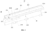
- FIG. 3 is a first perspective view of a portion of the housing assembly in accordance with an embodiment of the present disclosure.
- the housing assembly 20 includes a main body 21 and a metal frame 22.
- the main body 21 is configured to provide support for the electronic components and functional assemblies in the electronic device 100.
- the main body 21 may be provided with a plurality of recesses, through-holes, projections, and other structures for mounting the electronic components or functional assemblies or for cooperating with a structure of the electronic components or functional assemblies.
- the main body 21 includes a side edge 211, the side edge 211 may be an edge of the main body 21.
- the side edge 211 is connect to the metal frame 22.
- the metal frame 22 is disposed around the main body 21.
- the metal frame 22 may be disposed around the circumference of the main body 21 to form an outer frame of the housing assembly 20.
- the metal frame 22 is connected to the side edge 211.
- the material of the metal frame 22 may include metal or alloy.
- the metal frame 22 may be made of metal such as aluminum alloy, magnesium alloy, etc.
- the metal frame 22 is relatively stiff to serve as a support in the electronic device 100.
- the metal frame 22 includes a bezel portion 221 and a carrying portion 222.
- the bezel portion 221 is connected to the carrying portion 222.
- the bezel portion 221 is configured to form an outer frame of the housing assembly 20.
- the carrying portion 222 is configured to connect to the back cover 50. In other words, the carrying portion 222 is configured to carry the back cover 50 of the electronic device 100, and enabling the connection of the back cover 50 to the housing assembly 20.
- the carrying portion 222 may be provided with a bonding adhesive, he bonding adhesive is configured to bond with the back cover 50, and enable the connection of the carrying portion 222 to the back cover 50.
- the bezel portion 221 is connected to the side edge 211 of the main body 21 and extends along a thickness direction of the main body 21 and away the main body 21.
- the bezel portion 221 may extend upwardly along the thickness direction of the main body 21.
- the bezel portion 221 and the main body 21 may cooperatively define an accommodating portion 210.
- the accommodating portion 210 can be referred as an accommodating space or an empty three-dimensional area.
- the carrying portion 222 is disposed along the bezel portion 221 in the accommodating portion 210 and connected to the bezel portion 221 and the main body 21.
- a first groove 231 is defined between the carrying portion 222 and the bezel portion 221, a second groove 232 is defined between the carrying portion 222 and the main body 21.
- the first groove 231 is connected to the second groove 232 to form a metal arm 2220 on the carrying portion 222.
- the main body 21 and the metal frame 22 may be integrally molded with one another.
- the main body 21 and the metal frame 22 may be integrally molded by injection molding.
- the first groove 231, the second groove 232 may be formed by machining on the metal frame 22 after the housing assembly 20 has been integrally molded.
- the first groove 231 and the second groove 232 may be machined on the metal frame 22 by turning or milling, etc.
- the metal arm 2220 is spaced apart from the bezel portion 221. In other words, the metal arm 2220 is not connected to the bezel portion 221.
- the metal arm 2220 is spaced apart from the main body 21. In other words, the metal arm 2220 is not connected to the main body 21.
- the metal arm 2220 may be configured to form an antenna radiator 2221.
- the antenna radiator 2221 may be configured to transmit RF signals for the electronic device 100.
- the antenna radiator 2221 may be configured to transmit cellular network signals, Wireless Fidelity (Wi-Fi) signals, Global Positioning System (GPS) signals, etc.
- a length of the antenna radiator 2221 formed on the metal arm 2220 may be approximately 10mm to 20mm, a width of the antenna radiator 2221 may be approximately 1mm to 2mm, and a thickness of the antenna radiator 2221 may be approximately 0.5mm to 2mm.
- the carrying portion 222 may be defined with a third groove 233.
- the third groove 233 is connected to the first groove 231 and the second groove 232 so that a free end is formed on one side of the metal arm 2220.
- the third groove 233 may be defined perpendicular to the first groove 231 and the second groove 232, so that the third groove 233 is connected to both the first groove 231 and the second groove 232.
- the third groove 233 may also be formed by machining on the metal frame 22 after the housing assembly 20 has been integrally molded.
- the third groove 233 may be machined on the metal frame 22 by turning or milling, etc.
- the structural strength of the housing assembly 20 may be affected, which leads to the structural strength of the housing assembly 20 reduced.
- the first groove 231, the second groove 232, and the third groove 233 may be filled with insulating materials.
- the first groove 231, the second groove 232, and the third groove 233 may be filled with plastic, for example, by injection molding the first groove 231, the second groove 232, and the third groove 233.
- the antenna radiator 2221 formed by the metal arm 2220 may be provided with a feeding point 2221a and a grounding point 2221b (as shown in FIG. 4 ) being spaced apart from each other.
- the feeding point 2221a is configured for feeding RF signals onto the antenna radiator 2221
- the grounding point 2221b is configured for grounding.
- the electronic device 100 may be provided with a signal source on the circuit board 30, and the signal source is configured to generate RF signals.
- the feeding point 2221a may be electrically connected to the signal source to enable the signal source to feed the RF signals onto the antenna radiator 2221 through the feeding point 2221 a.
- the circuit board 30 of the electronic device 100 may be provided with a grounding point which forms a system ground of the electronic device 100.
- the grounding point 2221b on the antenna radiator 2221 may be electrically connected to the grounding point provided on the circuit board 30 to achieve grounding of the antenna radiator 2221.
- feeding point may also be referred as feed point or feed in point, etc.
- grounding point may also be referred as ground feed point, ground return point or ground, etc.
- FIG. 4 is a second perspective view of a portion of the housing assembly 20 in accordance with an embodiment of the present disclosure.
- the antenna radiator 2221 formed by the metal arm 2220 may be provided with a first metal protrusion 222A and a second metal protrusion 222B.
- the first metal protrusion 222A and the second metal protrusion 222B may be metal blocks formed on the metal arm 2220.
- the feeding point 2221a provided on the antenna radiator 2221 includes the first metal protrusion 222A
- the grounding point 2221b provided on the antenna radiator 2221 includes the second metal protrusion 222B.
- the first metal protrusion 222A may be electrically connected to the signal source provided on the circuit board 30 by means of a metal shrapnel or a metal screw, etc.
- the second metal protrusion 222B may be electrically connected to the grounding point provided on the circuit board 30 by means of a metal shrapnel or a metal screw, etc.
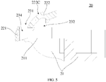
- FIG. 5 is a section view of the housing assembly along with profile line P2-P2 shown in FIG.3 .
- the bonding surface between the carrying portion 222 and the rear cover 50 can be designed.
- An arc-shaped carrying surface 222C can be formed on the side of the carrying portion 222 back from the main body 21. It is understood that the arc-shaped carrying surface 222C can increase the area of the bonding surface between the carrying portion 222 and the rear cover 50, thus making the bonding between the carrying portion 222 and the rear cover 50 more stable.
- the thickness of the carrying portion 222 increases non-linearly in a direction away from the side edge 211 of the main body 21. In other words, the thickness of the carrying portion 222 increases unevenly.
- the height of the second groove 232 increases non-linearly in a direction away from the side edge 211 of the main body 21. In other words, the height of the second groove 232 increases unevenly. In some embodiments, the height of the second groove 232 may vary in the same way as the thickness of the carrying portion 222. Thereby, it is possible to make the thickness of the metal arm 2220 formed on the carrying portion 222 the same along its width so that the current on the antenna radiator 2221 is uniformly distributed along its width when transmitting the RF signals, which improves the performance of the antenna radiator 2221 when transmitting the RF signals.
- the carrying portion 222 is defined with a recess 234 at the connection with the bezel portion 221.
- the first groove 231 may be connected to the recess 234. Wherein the first groove 231 has a same width as the recess 234, which forms a smooth connection of the load carrying portion 222 with the bezel portion 221.
- the metal arm 2220 can form an antenna radiator 2221, the antenna radiator 2221 can be configured to transmit RF signals, and thus the housing assembly 20 can be reused as antennas to achieve the RF signals transmission function, thus a separate antenna radiator is not needed, and effectively saving the internal space of the electronic device 100.
Landscapes
- Engineering & Computer Science (AREA)
- Computer Networks & Wireless Communication (AREA)
- Support Of Aerials (AREA)
- Telephone Set Structure (AREA)
- Casings For Electric Apparatus (AREA)
Abstract
Description
- The present disclosure claims priority to
Chinese Patent Application No. 2019107659525, filed on August 19, 2019 - The present disclosure relates to electronic technology, and more particularly, to a housing assembly and electronic device.
- With the development of electronic technology, users can realize more and more functions through electronic devices such as smart phones, especially various network functions, such as voice calls, video chats, online games, etc.
- In the process of voice calls, video chats and online games, the electronic devices need to communicate with base station or server for data interaction, and in the process of data interaction, the electronic devices need to transmit Radio-Frequency (RF) signals through antenna.
- On the other hand, with the development of electronic technology, electronic devices are getting smaller and thinner, and the internal space of electronic devices is getting smaller. Thus, how to reasonably design the antenna to save the internal space of electronic devices becomes a problem in the field.
- The present disclosure provides a housing assembly and an electronic device, RF signals can be transmitted through the housing assembly, which saves the internal space of the electronic device.
- In a first aspect, the present disclosure provides a housing assembly, the housing assembly includes a main body and a metal frame. The main body includes a side edge, the metal frame includes a bezel portion and a carrying portion. The bezel portion is connected to the side edge and extends along a thickness direction of the main body. The bezel portion and the main body cooperatively defines an accommodating portion. The carrying portion is located in the accommodating portion and disposed along the bezel portion, and the carrying portion is connected to the bezel portion and the main body. A first groove is defined between the carrying portion and the bezel portion, and a second groove is defined between the carrying portion and the main body. The first groove is connected to the second groove to form a metal arm on the carrying portion, the metal arm is configured to form an antenna radiator.
- In a second aspect, the present disclosure provides an electronic device, the electronic device includes a housing assembly and a back cover. The housing assembly includes a main body and a metal frame. The main body includes a side edge, the metal frame includes a bezel portion and a carrying portion. The bezel portion is connected to the side edge and extends along a thickness direction of the main body. The bezel portion and the main body cooperatively defines an accommodating portion. The carrying portion is located in the accommodating portion and disposed along the bezel portion, and the carrying portion is connected to the bezel portion and the main body. A first groove is defined between the carrying portion and the bezel portion, and a second groove is defined between the carrying portion and the main body. The first groove is connected to the second groove to form a metal arm on the carrying portion, the metal arm is configured to form an antenna radiator. The back cover is connected to the carrying portion.
- To clearly explain technical solutions of embodiments of the present disclosure, drawings used in embodiments are briefly described below. The drawings as described below are merely some embodiments of the present disclosure. Based on these drawings, other obvious variants can be obtained by those skilled in the art without creative effort.
-
FIG. 1 is a schematic front view of an electronic device in accordance with an embodiment of the present disclosure. -
FIG. 2 is a section view of the electronic device along with profile line P1-P1 shown inFIG. 1 . -
FIG. 3 is a first perspective view of a portion of the housing assembly in accordance with an embodiment of the present disclosure. -
FIG. 4 is a second perspective view of a portion of the housing assembly in accordance with an embodiment of the present disclosure. -
FIG. 5 is a section view of the housing assembly along with profile line P2-P2 shown inFIG.3 . - The technical solutions of embodiments of the present disclosure will be clearly and completely described below in conjunction with the drawings. It should be understood that the described embodiments are not limiting and are not the only contemplated embodiments of the present disclosure. Based on the embodiments in the present disclosure, all other variants obtained by a person skilled in the art without creative effort shall fall within the scope of protection of the present disclosure.
- An electronic device is provided according to an embodiment of the present disclosure. The electronic device may be a device such as a smartphone, a tablet computer, etc., and may also be a gaming device, an Augmented Reality (AR) device, an automotive device, a data storage device, an audio playback device, a video playback device, a laptop computer, a desktop computing device, etc.
- As illustrated in
FIG. 1 andFIG. 2 , whereinFIG. 1 is a schematic front view of anelectronic device 100 according to an embodiment of the present disclosure, andFIG. 2 is a section view of theelectronic device 100 along with profile line P1-P1 shown inFIG.1 . - The
electronic device 100 includes adisplay 10, ahousing assembly 20, acircuit board 30, abattery 40, and aback cover 50. - The
display 10 is mounted on thehousing assembly 20 to form a display surface of theelectronic device 100 for displaying information such as images, text, etc. Thedisplay 10 may include a Liquid Crystal Display (LCD) or an Organic Light-Emitting Diode Display (OLED). - The
display 10 may also be provided with a cover plate to protect thedisplay 10 from being scratched or damaged by water. The cover plate may be a transparent glass cover plate, so that the content displayed on thedisplay 10 can be observed by a user through the cover plate. The cover plate may be a sapphire glass cover plate, for example. - The
housing assembly 20 may be a sheet or have a lamellar structure, or a hollow frame structure. Thehousing assembly 20 is configured to provide support for electronic components or functional assemblies in theelectronic device 100. For example, thehousing assembly 20 may be provided with recesses, projections, through-holes, and other structures on/in which to mount the electronic components or functional assemblies of theelectronic device 100. Thehousing assembly 20 may be a middle frame of theelectronic device 100. - The
housing assembly 20 and theback cover 50 may form a housing together for accommodating the electronic components and functional assemblies of theelectronic device 100. For example, cameras, receivers, circuit boards, battery, and other functional components of theelectronic device 100 may be mounted to thehousing assembly 20 for securing and accommodating such components within the housing. The material of thehousing assembly 20 may include some form or type of metal or plastic. - The
circuit board 30 is mounted inside the housing formed by thehousing assembly 20 together with theback cover 50. For example, thecircuit board 30 may be mounted on thehousing assembly 20 and accommodated inside the housing. Thecircuit board 30 may be a main board of theelectronic device 100. Thecircuit board 30 may be provided with an RF (Radio Frequency) circuit. The RF circuit is configured to generate RF signals and transmit the RF signals via an antenna radiator of theelectronic device 100, and process RF signals received by the antenna radiator. In addition, one or more functional assemblies such as microphones, speakers, receivers, headphone interfaces, cameras, accelerometers, gyroscopes, and processors may be integrated on thecircuit board 30. Thedisplay 10 may be electrically connected to thecircuit board 30, and being controlled by a processor mounted on thecircuit board 30. - The
battery 40 is mounted inside the housing formed by thehousing assembly 20 together with theback cover 50. For example, thebattery 40 may be mounted to thehousing assembly 20 and accommodated inside the housing. Thebattery 40 is electrically connected to thecircuit board 30 to enable thebattery 40 to power theelectronic device 100. Thecircuit board 30 may be provided with a power management circuit. The power management circuit is configured to allocate the voltage provided by thebattery 40 to the various electronic components in theelectronic device 100. - The
back cover 50 is connected to thehousing assembly 20. For example, theback cover 50 may be attached to thehousing assembly 20 by an adhesive such as a double-sided adhesive. Theback cover 50 is configured to seal the electronic components and functional assemblies of theelectronic device 100 inside theelectronic device 100 in conjunction with thehousing assembly 20 and thedisplay 10 to protect the electronic components and the functional assemblies. Theback cover 50 may also be referred to as a battery cover. It is understood that theback cover 50 may be molded in one piece. A structure such as a rear camera mounting hole may be defined in theback cover 50. The rear camera mounting hole may be formed during the molding of theback cover 50. -
FIG. 3 is a first perspective view of a portion of the housing assembly in accordance with an embodiment of the present disclosure. - As illustrated in
FIG. 3 , thehousing assembly 20 includes amain body 21 and ametal frame 22. - The
main body 21 is configured to provide support for the electronic components and functional assemblies in theelectronic device 100. For example, themain body 21 may be provided with a plurality of recesses, through-holes, projections, and other structures for mounting the electronic components or functional assemblies or for cooperating with a structure of the electronic components or functional assemblies. - The
main body 21 includes aside edge 211, theside edge 211 may be an edge of themain body 21. Theside edge 211 is connect to themetal frame 22. - The
metal frame 22 is disposed around themain body 21. For example, themetal frame 22 may be disposed around the circumference of themain body 21 to form an outer frame of thehousing assembly 20. Themetal frame 22 is connected to theside edge 211. The material of themetal frame 22 may include metal or alloy. For example, themetal frame 22 may be made of metal such as aluminum alloy, magnesium alloy, etc. Themetal frame 22 is relatively stiff to serve as a support in theelectronic device 100. - The
metal frame 22 includes abezel portion 221 and a carryingportion 222. Thebezel portion 221 is connected to the carryingportion 222. Thebezel portion 221 is configured to form an outer frame of thehousing assembly 20. The carryingportion 222 is configured to connect to theback cover 50. In other words, the carryingportion 222 is configured to carry theback cover 50 of theelectronic device 100, and enabling the connection of theback cover 50 to thehousing assembly 20. - For example, the carrying
portion 222 may be provided with a bonding adhesive, he bonding adhesive is configured to bond with theback cover 50, and enable the connection of the carryingportion 222 to theback cover 50. - The
bezel portion 221 is connected to theside edge 211 of themain body 21 and extends along a thickness direction of themain body 21 and away themain body 21. For example, thebezel portion 221 may extend upwardly along the thickness direction of themain body 21. Thebezel portion 221 and themain body 21 may cooperatively define anaccommodating portion 210. Theaccommodating portion 210 can be referred as an accommodating space or an empty three-dimensional area. The carryingportion 222 is disposed along thebezel portion 221 in theaccommodating portion 210 and connected to thebezel portion 221 and themain body 21. - A
first groove 231 is defined between the carryingportion 222 and thebezel portion 221, asecond groove 232 is defined between the carryingportion 222 and themain body 21. Thefirst groove 231 is connected to thesecond groove 232 to form ametal arm 2220 on the carryingportion 222. - In the
housing assembly 20, themain body 21 and themetal frame 22 may be integrally molded with one another. For example, themain body 21 and themetal frame 22 may be integrally molded by injection molding. Thefirst groove 231, thesecond groove 232 may be formed by machining on themetal frame 22 after thehousing assembly 20 has been integrally molded. For example, thefirst groove 231 and thesecond groove 232 may be machined on themetal frame 22 by turning or milling, etc. - Since the
first groove 231 is defined between the carryingportion 222 and thebezel portion 221, themetal arm 2220 is spaced apart from thebezel portion 221. In other words, themetal arm 2220 is not connected to thebezel portion 221. Similarly, since thesecond groove 232 is defined between the carryingportion 222 and themain body 21, themetal arm 2220 is spaced apart from themain body 21. In other words, themetal arm 2220 is not connected to themain body 21. - The
metal arm 2220 may be configured to form anantenna radiator 2221. Theantenna radiator 2221 may be configured to transmit RF signals for theelectronic device 100. For example, the antenna radiator 2221may be configured to transmit cellular network signals, Wireless Fidelity (Wi-Fi) signals, Global Positioning System (GPS) signals, etc. - A length of the
antenna radiator 2221 formed on themetal arm 2220 may be approximately 10mm to 20mm, a width of theantenna radiator 2221 may be approximately 1mm to 2mm, and a thickness of theantenna radiator 2221 may be approximately 0.5mm to 2mm. - As illustrated in
FIG. 3 , the carryingportion 222 may be defined with athird groove 233. Thethird groove 233 is connected to thefirst groove 231 and thesecond groove 232 so that a free end is formed on one side of themetal arm 2220. In some embodiments, thethird groove 233 may be defined perpendicular to thefirst groove 231 and thesecond groove 232, so that thethird groove 233 is connected to both thefirst groove 231 and thesecond groove 232. - The
third groove 233 may also be formed by machining on themetal frame 22 after thehousing assembly 20 has been integrally molded. For example, thethird groove 233 may be machined on themetal frame 22 by turning or milling, etc. - Since the
first groove 231, thesecond groove 232, and thethird groove 233 are defined on thehousing assembly 20, the structural strength of thehousing assembly 20 may be affected, which leads to the structural strength of thehousing assembly 20 reduced. Thereby, to improve the structural strength of thehousing assembly 20, thefirst groove 231, thesecond groove 232, and thethird groove 233 may be filled with insulating materials. For example, thefirst groove 231, thesecond groove 232, and thethird groove 233 may be filled with plastic, for example, by injection molding thefirst groove 231, thesecond groove 232, and thethird groove 233. - The
antenna radiator 2221 formed by themetal arm 2220 may be provided with afeeding point 2221a and agrounding point 2221b (as shown inFIG. 4 ) being spaced apart from each other. Thefeeding point 2221a is configured for feeding RF signals onto theantenna radiator 2221, and thegrounding point 2221b is configured for grounding. For example, theelectronic device 100 may be provided with a signal source on thecircuit board 30, and the signal source is configured to generate RF signals. Thefeeding point 2221a may be electrically connected to the signal source to enable the signal source to feed the RF signals onto theantenna radiator 2221 through thefeeding point 2221 a. In addition, thecircuit board 30 of theelectronic device 100 may be provided with a grounding point which forms a system ground of theelectronic device 100. Thegrounding point 2221b on theantenna radiator 2221 may be electrically connected to the grounding point provided on thecircuit board 30 to achieve grounding of theantenna radiator 2221. - It should be noted that the feeding point may also be referred as feed point or feed in point, etc., and the grounding point may also be referred as ground feed point, ground return point or ground, etc.
-
FIG. 4 is a second perspective view of a portion of thehousing assembly 20 in accordance with an embodiment of the present disclosure. - As illustrated in
FIG. 4 , theantenna radiator 2221 formed by themetal arm 2220 may be provided with afirst metal protrusion 222A and asecond metal protrusion 222B. In at least one embodiment, thefirst metal protrusion 222A and thesecond metal protrusion 222B may be metal blocks formed on themetal arm 2220. Wherein thefeeding point 2221a provided on theantenna radiator 2221 includes thefirst metal protrusion 222A, thegrounding point 2221b provided on theantenna radiator 2221 includes thesecond metal protrusion 222B. - The
first metal protrusion 222A may be electrically connected to the signal source provided on thecircuit board 30 by means of a metal shrapnel or a metal screw, etc. Thesecond metal protrusion 222B may be electrically connected to the grounding point provided on thecircuit board 30 by means of a metal shrapnel or a metal screw, etc. -
FIG. 5 is a section view of the housing assembly along with profile line P2-P2 shown inFIG.3 . - As illustrated in
FIG. 5 , to make the connection between the carryingportion 222 and therear cover 50 of theelectronic device 100 more stable, the bonding surface between the carryingportion 222 and therear cover 50 can be designed. An arc-shapedcarrying surface 222C can be formed on the side of the carryingportion 222 back from themain body 21. It is understood that the arc-shapedcarrying surface 222C can increase the area of the bonding surface between the carryingportion 222 and therear cover 50, thus making the bonding between the carryingportion 222 and therear cover 50 more stable. In some embodiments, the thickness of the carryingportion 222 increases non-linearly in a direction away from theside edge 211 of themain body 21. In other words, the thickness of the carryingportion 222 increases unevenly. - In some embodiments, the height of the
second groove 232 increases non-linearly in a direction away from theside edge 211 of themain body 21. In other words, the height of thesecond groove 232 increases unevenly. In some embodiments, the height of thesecond groove 232 may vary in the same way as the thickness of the carryingportion 222. Thereby, it is possible to make the thickness of themetal arm 2220 formed on the carryingportion 222 the same along its width so that the current on theantenna radiator 2221 is uniformly distributed along its width when transmitting the RF signals, which improves the performance of theantenna radiator 2221 when transmitting the RF signals. - Refer to
FIG. 5 , wherein the carryingportion 222 is defined with arecess 234 at the connection with thebezel portion 221. Thefirst groove 231 may be connected to therecess 234. Wherein thefirst groove 231 has a same width as therecess 234, which forms a smooth connection of theload carrying portion 222 with thebezel portion 221. - According to the
housing assembly 20 provided in the present disclosure, since ametal arm 2220 is formed on themetal frame 22, themetal arm 2220 can form anantenna radiator 2221, theantenna radiator 2221 can be configured to transmit RF signals, and thus thehousing assembly 20 can be reused as antennas to achieve the RF signals transmission function, thus a separate antenna radiator is not needed, and effectively saving the internal space of theelectronic device 100. - In the description of the present disclosure, it is to be understood that terms such as "first" and "second" are used only to distinguish similar objects and are not to be understood as indicating or implying relative importance or implicitly specifying the number of technical features indicated.
- The above provides a detailed description of the housing assembly and the electronic device provided in accordance with embodiments of the present disclosure. Specific examples have been applied herein to illustrate the principles and implementation of the present disclosure, and the above description of embodiments is only for helping to understand the present disclosure. At the same time, for a skilled person in the art, according to the idea of the present disclosure, there will be changes in the specific implementation and the scope of application, in summary, the content of this specification should not be understood as a limitation of the present disclosure.
Claims (20)
- A housing assembly, comprising:a main body, comprising a side edge;a metal frame, wherein the metal frame comprises a bezel portion and a carrying portion, the bezel portion being connected to the side edge and extending along a thickness direction of the main body, the bezel portion and the main body cooperatively defining an accommodating portion, the carrying portion being located in the accommodating portion and disposed along the bezel portion, the carrying portion being connected to the bezel portion and the main body; anda first groove defined between the carrying portion and the bezel portion, and a second groove defined between the carrying portion and the main body, wherein the first groove is connected to the second groove, and a metal arm being formed on the carrying portion, the metal arm being configured to form an antenna radiator.
- The housing assembly according to claim 1, wherein a third groove is defined in the carrying portion, the third groove being connected to the first groove and the second groove, and a free end is formed on one side of the metal arm.
- The housing assembly according to claim 2, wherein the first groove, the second groove, and the third groove are filled with insulating materials.
- The housing assembly according to claim 1, wherein a feeding point and a grounding point are provided on the antenna radiator and spaced apart from each other.
- The housing assembly according to claim 4, wherein the feeding point comprises a first metal protrusion provided on the antenna radiator, and wherein the grounding point comprises a second metal protrusion provided on the antenna radiator.
- The housing assembly according to claim 1, wherein a thickness of the carrying portion increases non-linearly in a direction away from the side edge of the main body, and an arc-shaped carrying surface is formed on the side of the carrying portion back from the main body.
- The housing assembly according to claim 6, wherein a height of the second groove increases non-linearly in a direction away from the side edge of the main body, and wherein the thickness of the metal arm formed on the carrying portion is uniform along the metal arm's width.
- The housing assembly according to claim 1, wherein the carrying portion is defined with a recess at the connection with the bezel portion, and wherein the first groove has a same width as the recess.
- The housing assembly according to claim 1, wherein the main body and the metal frame are integrally molded with one another, the first groove and the second groove being machined grooves on the metal frame after the housing assembly has been integrally molded.
- The housing assembly according to claim 1, wherein a length of the antenna radiator formed on the metal arm is approximately 10mm to 20mm, a width of the antenna radiator is approximately 1mm to 2mm, and a thickness of the antenna radiator is approximately 0.5mm to 2mm.
- An electronic device, comprising a housing assembly and a back cover, wherein the housing assembly comprising:a main body, comprising a side edge;a metal frame, comprising a bezel portion and a carrying portion, the bezel portion being connected to the side edge and extending along a thickness direction of the main body, the bezel portion and the main body cooperatively defining an accommodating portion, the carrying portion being located in the accommodating portion disposed along the bezel portion, and the carrying portion being connected to the bezel portion and the main body;a first groove defined between the carrying portion and the bezel portion, and a second groove defined between the carrying portion and the main body, wherein the first groove is connected to the second groove, a metal arm being formed on the carrying portion, the metal arm being configured to form an antenna radiator; andthe back cover is connected to the carrying portion.
- The electronic device according to claim 11, wherein a third groove is defined in the carrying portion, the third groove being connected to the first groove and the second groove, and a free end being formed on one side of the metal arm.
- The electronic device according to claim 12, wherein the first groove, the second groove, and the third groove are filled with insulating materials.
- The electronic device according to claim 11, wherein a feeding point and a grounding point are provided on the antenna radiator and spaced apart from each other.
- The electronic device according to claim 14, wherein the feeding point comprises a first metal protrusion provided on the antenna radiator, and wherein the grounding point comprises a second metal protrusion provided on the antenna radiator.
- The electronic device according to claim 11, wherein a thickness of the carrying portion increases non-linearly in a direction away from the side edge of the main body, and an arc-shaped carrying surface is formed on the side of the carrying portion back from the main body.
- The electronic device according to claim 16, wherein a height of the second groove increases non-linearly in a direction away from the side edge of the main body, the thickness of the metal arm formed on the carrying portion is uniform across a width of the metal arm.
- The electronic device according to claim 11, wherein the carrying portion is defined with a recess at the connection with the bezel portion, a width of the first groove and the recess being the same.
- The electronic device according to claim 11, wherein the main body and the metal frame are integrally molded with one another, the first groove and the second groove being machined grooves on the metal frame after the housing assembly has been integrally molded.
- The electronic device according to claim 11, wherein a length of the antenna radiator formed on the metal arm is approximately 10mm to 20mm, a width of the antenna radiator is approximately 1mm to 2mm, and a thickness of the antenna radiator is approximately 0.5mm to 2mm.
Applications Claiming Priority (2)
| Application Number | Priority Date | Filing Date | Title |
|---|---|---|---|
| CN201910765952.5A CN110459872B (en) | 2019-08-19 | 2019-08-19 | Housing components and electronic equipment |
| PCT/CN2020/107486 WO2021031870A1 (en) | 2019-08-19 | 2020-08-06 | Housing assembly and electronic device |
Publications (3)
| Publication Number | Publication Date |
|---|---|
| EP4012838A1 true EP4012838A1 (en) | 2022-06-15 |
| EP4012838A4 EP4012838A4 (en) | 2022-10-12 |
| EP4012838B1 EP4012838B1 (en) | 2024-05-29 |
Family
ID=68487685
Family Applications (1)
| Application Number | Title | Priority Date | Filing Date |
|---|---|---|---|
| EP20855786.8A Active EP4012838B1 (en) | 2019-08-19 | 2020-08-06 | Housing assembly and electronic device |
Country Status (4)
| Country | Link |
|---|---|
| US (1) | US12027757B2 (en) |
| EP (1) | EP4012838B1 (en) |
| CN (1) | CN110459872B (en) |
| WO (1) | WO2021031870A1 (en) |
Families Citing this family (2)
| Publication number | Priority date | Publication date | Assignee | Title |
|---|---|---|---|---|
| CN110459872B (en) | 2019-08-19 | 2021-07-16 | Oppo广东移动通信有限公司 | Housing components and electronic equipment |
| CN117255505A (en) * | 2022-06-10 | 2023-12-19 | 北京小米移动软件有限公司 | Housing components and electronic equipment |
Family Cites Families (23)
| Publication number | Priority date | Publication date | Assignee | Title |
|---|---|---|---|---|
| CN101466214B (en) * | 2007-12-20 | 2012-01-25 | 神基科技股份有限公司 | Housing structure of electronic device |
| US8656579B2 (en) * | 2008-08-29 | 2014-02-25 | Motorola Mobility Llc | Method of forming a housing with integral antenna |
| US8963785B2 (en) * | 2012-12-27 | 2015-02-24 | Auden Techno. Corp. | Antenna structure for using with a metal frame of a mobile phone |
| US9531059B2 (en) * | 2013-05-24 | 2016-12-27 | Microsoft Technology Licensing, Llc | Side face antenna for a computing device case |
| KR102094754B1 (en) * | 2013-12-03 | 2020-03-30 | 엘지전자 주식회사 | Mobile terminal |
| CN104852127A (en) * | 2014-02-17 | 2015-08-19 | 深圳富泰宏精密工业有限公司 | Antenna structure, electronic device employing same, and manufacturing method for antenna structure |
| CN208273029U (en) * | 2014-09-08 | 2018-12-21 | 苹果公司 | Shell and mobile phone |
| US10148000B2 (en) * | 2015-09-04 | 2018-12-04 | Apple Inc. | Coupling structures for electronic device housings |
| KR101827275B1 (en) * | 2015-11-27 | 2018-02-08 | 엘지전자 주식회사 | Mobile terminal |
| US10389857B2 (en) * | 2015-12-17 | 2019-08-20 | Huawei Technologies Co., Ltd. | Mobile communications terminal |
| CN106910977A (en) * | 2015-12-22 | 2017-06-30 | 华硕电脑股份有限公司 | Portable electronic device |
| KR102510098B1 (en) * | 2016-05-19 | 2023-03-13 | 엘에스엠트론 주식회사 | Antenna device for mobile communication terminal |
| US10566681B2 (en) * | 2016-07-21 | 2020-02-18 | Chiun Mai Communication Systems, Inc. | Antenna structure and wireless communication device using same |
| US10320063B2 (en) * | 2016-12-14 | 2019-06-11 | Fitbit, Inc. | Methods for slot antenna design for wearable electronic devices and conductive housings |
| CN107087364A (en) * | 2017-05-09 | 2017-08-22 | 广东欧珀移动通信有限公司 | Metal middle frame processing technology, metal middle frame and electronic device |
| CN109216875B (en) * | 2017-06-30 | 2020-11-13 | 惠州硕贝德无线科技股份有限公司 | A Broadband Antenna with Reflector and Antenna System |
| KR20190011169A (en) * | 2017-07-24 | 2019-02-01 | 삼성전자주식회사 | Electronic device and manufacturing method for housing of the same |
| CN108174541A (en) * | 2017-11-30 | 2018-06-15 | 维沃移动通信有限公司 | A kind of metal shell and preparation method thereof, mobile terminal |
| CN108039582A (en) | 2017-12-01 | 2018-05-15 | 广东欧珀移动通信有限公司 | Middle frame components, antenna components and electronic equipment |
| CN108417966A (en) * | 2018-01-25 | 2018-08-17 | 瑞声科技(新加坡)有限公司 | A kind of antenna system and mobile terminal |
| CN108925073B (en) * | 2018-06-26 | 2021-03-05 | Oppo广东移动通信有限公司 | Electronic equipment and casing, casing subassembly thereof |
| CN109905505B (en) * | 2019-03-20 | 2020-09-04 | Oppo广东移动通信有限公司 | Shell and electronic equipment |
| CN110459872B (en) * | 2019-08-19 | 2021-07-16 | Oppo广东移动通信有限公司 | Housing components and electronic equipment |
-
2019
- 2019-08-19 CN CN201910765952.5A patent/CN110459872B/en active Active
-
2020
- 2020-08-06 EP EP20855786.8A patent/EP4012838B1/en active Active
- 2020-08-06 WO PCT/CN2020/107486 patent/WO2021031870A1/en not_active Ceased
-
2022
- 2022-02-14 US US17/671,389 patent/US12027757B2/en active Active
Also Published As
| Publication number | Publication date |
|---|---|
| WO2021031870A1 (en) | 2021-02-25 |
| EP4012838A4 (en) | 2022-10-12 |
| US12027757B2 (en) | 2024-07-02 |
| EP4012838B1 (en) | 2024-05-29 |
| US20220173503A1 (en) | 2022-06-02 |
| CN110459872B (en) | 2021-07-16 |
| CN110459872A (en) | 2019-11-15 |
Similar Documents
| Publication | Publication Date | Title |
|---|---|---|
| CN112768904B (en) | Antenna radiator, antenna assembly and electronic equipment | |
| CN112164881B (en) | Camera decoration parts, antenna devices and electronic equipment | |
| CN108736134B (en) | Antenna components and electronic equipment | |
| US12027757B2 (en) | Housing assembly and electronic device | |
| CN112993579A (en) | Antenna device and electronic apparatus | |
| CN108550979B (en) | Antenna assemblies, housing assemblies and electronic equipment | |
| CN109346828B (en) | Antenna assembly and electronic equipment | |
| US11949152B2 (en) | Antenna device and electronic device | |
| CN110572498A (en) | Assembling method of shell assembly, shell assembly and electronic device | |
| CN108493575B (en) | Antenna components and electronic equipment | |
| CN112103624B (en) | Antenna device and electronic apparatus | |
| CN108666739B (en) | Antenna assembly, shell assembly and electronic equipment | |
| CN208522831U (en) | Housing unit and electronic equipment | |
| CN110492233B (en) | Shell assembly and electronic equipment | |
| CN114843745A (en) | Antenna assembly, preparation method thereof, shell assembly and electronic equipment | |
| CN108565561A (en) | Antenna assembly and electronic equipment | |
| CN108281764A (en) | Antenna assembly and electronic equipment | |
| CN208820049U (en) | Antenna components and electronic equipment | |
| CN108539376B (en) | Shell assembly, antenna assembly, manufacturing method of antenna assembly and electronic equipment | |
| CN111447352A (en) | Brackets, camera components and terminal equipment | |
| US20220336952A1 (en) | Antenna device and electronic device | |
| WO2020001186A1 (en) | Electronic device | |
| CN214378862U (en) | Antenna systems and electronic equipment | |
| CN108965516B (en) | Electronic device | |
| CN108493574B (en) | Antenna components and electronic equipment |
Legal Events
| Date | Code | Title | Description |
|---|---|---|---|
| STAA | Information on the status of an ep patent application or granted ep patent |
Free format text: STATUS: THE INTERNATIONAL PUBLICATION HAS BEEN MADE |
|
| PUAI | Public reference made under article 153(3) epc to a published international application that has entered the european phase |
Free format text: ORIGINAL CODE: 0009012 |
|
| STAA | Information on the status of an ep patent application or granted ep patent |
Free format text: STATUS: REQUEST FOR EXAMINATION WAS MADE |
|
| 17P | Request for examination filed |
Effective date: 20220311 |
|
| AK | Designated contracting states |
Kind code of ref document: A1 Designated state(s): AL AT BE BG CH CY CZ DE DK EE ES FI FR GB GR HR HU IE IS IT LI LT LU LV MC MK MT NL NO PL PT RO RS SE SI SK SM TR |
|
| A4 | Supplementary search report drawn up and despatched |
Effective date: 20220912 |
|
| RIC1 | Information provided on ipc code assigned before grant |
Ipc: H01Q 1/24 20060101ALI20220906BHEP Ipc: H01Q 9/04 20060101ALI20220906BHEP Ipc: H01Q 1/36 20060101ALI20220906BHEP Ipc: H01Q 1/44 20060101AFI20220906BHEP |
|
| DAV | Request for validation of the european patent (deleted) | ||
| DAX | Request for extension of the european patent (deleted) | ||
| GRAP | Despatch of communication of intention to grant a patent |
Free format text: ORIGINAL CODE: EPIDOSNIGR1 |
|
| STAA | Information on the status of an ep patent application or granted ep patent |
Free format text: STATUS: GRANT OF PATENT IS INTENDED |
|
| INTG | Intention to grant announced |
Effective date: 20240307 |
|
| GRAS | Grant fee paid |
Free format text: ORIGINAL CODE: EPIDOSNIGR3 |
|
| GRAA | (expected) grant |
Free format text: ORIGINAL CODE: 0009210 |
|
| STAA | Information on the status of an ep patent application or granted ep patent |
Free format text: STATUS: THE PATENT HAS BEEN GRANTED |
|
| AK | Designated contracting states |
Kind code of ref document: B1 Designated state(s): AL AT BE BG CH CY CZ DE DK EE ES FI FR GB GR HR HU IE IS IT LI LT LU LV MC MK MT NL NO PL PT RO RS SE SI SK SM TR |
|
| REG | Reference to a national code |
Ref country code: CH Ref legal event code: EP |
|
| REG | Reference to a national code |
Ref country code: IE Ref legal event code: FG4D |
|
| REG | Reference to a national code |
Ref country code: DE Ref legal event code: R096 Ref document number: 602020031793 Country of ref document: DE |
|
| REG | Reference to a national code |
Ref country code: LT Ref legal event code: MG9D |
|
| REG | Reference to a national code |
Ref country code: NL Ref legal event code: MP Effective date: 20240529 |
|
| PG25 | Lapsed in a contracting state [announced via postgrant information from national office to epo] |
Ref country code: IS Free format text: LAPSE BECAUSE OF FAILURE TO SUBMIT A TRANSLATION OF THE DESCRIPTION OR TO PAY THE FEE WITHIN THE PRESCRIBED TIME-LIMIT Effective date: 20240929 |
|
| PG25 | Lapsed in a contracting state [announced via postgrant information from national office to epo] |
Ref country code: BG Free format text: LAPSE BECAUSE OF FAILURE TO SUBMIT A TRANSLATION OF THE DESCRIPTION OR TO PAY THE FEE WITHIN THE PRESCRIBED TIME-LIMIT Effective date: 20240529 |
|
| P01 | Opt-out of the competence of the unified patent court (upc) registered |
Free format text: CASE NUMBER: APP_49632/2024 Effective date: 20240902 |
|
| PG25 | Lapsed in a contracting state [announced via postgrant information from national office to epo] |
Ref country code: HR Free format text: LAPSE BECAUSE OF FAILURE TO SUBMIT A TRANSLATION OF THE DESCRIPTION OR TO PAY THE FEE WITHIN THE PRESCRIBED TIME-LIMIT Effective date: 20240529 Ref country code: FI Free format text: LAPSE BECAUSE OF FAILURE TO SUBMIT A TRANSLATION OF THE DESCRIPTION OR TO PAY THE FEE WITHIN THE PRESCRIBED TIME-LIMIT Effective date: 20240529 |
|
| PG25 | Lapsed in a contracting state [announced via postgrant information from national office to epo] |
Ref country code: GR Free format text: LAPSE BECAUSE OF FAILURE TO SUBMIT A TRANSLATION OF THE DESCRIPTION OR TO PAY THE FEE WITHIN THE PRESCRIBED TIME-LIMIT Effective date: 20240830 |
|
| REG | Reference to a national code |
Ref country code: AT Ref legal event code: MK05 Ref document number: 1691428 Country of ref document: AT Kind code of ref document: T Effective date: 20240529 |
|
| PG25 | Lapsed in a contracting state [announced via postgrant information from national office to epo] |
Ref country code: ES Free format text: LAPSE BECAUSE OF FAILURE TO SUBMIT A TRANSLATION OF THE DESCRIPTION OR TO PAY THE FEE WITHIN THE PRESCRIBED TIME-LIMIT Effective date: 20240529 |
|
| PG25 | Lapsed in a contracting state [announced via postgrant information from national office to epo] |
Ref country code: AT Free format text: LAPSE BECAUSE OF FAILURE TO SUBMIT A TRANSLATION OF THE DESCRIPTION OR TO PAY THE FEE WITHIN THE PRESCRIBED TIME-LIMIT Effective date: 20240529 |
|
| PG25 | Lapsed in a contracting state [announced via postgrant information from national office to epo] |
Ref country code: PL Free format text: LAPSE BECAUSE OF FAILURE TO SUBMIT A TRANSLATION OF THE DESCRIPTION OR TO PAY THE FEE WITHIN THE PRESCRIBED TIME-LIMIT Effective date: 20240529 |
|
| PG25 | Lapsed in a contracting state [announced via postgrant information from national office to epo] |
Ref country code: LV Free format text: LAPSE BECAUSE OF FAILURE TO SUBMIT A TRANSLATION OF THE DESCRIPTION OR TO PAY THE FEE WITHIN THE PRESCRIBED TIME-LIMIT Effective date: 20240529 |
|
| PG25 | Lapsed in a contracting state [announced via postgrant information from national office to epo] |
Ref country code: PL Free format text: LAPSE BECAUSE OF FAILURE TO SUBMIT A TRANSLATION OF THE DESCRIPTION OR TO PAY THE FEE WITHIN THE PRESCRIBED TIME-LIMIT Effective date: 20240529 Ref country code: NO Free format text: LAPSE BECAUSE OF FAILURE TO SUBMIT A TRANSLATION OF THE DESCRIPTION OR TO PAY THE FEE WITHIN THE PRESCRIBED TIME-LIMIT Effective date: 20240829 Ref country code: LV Free format text: LAPSE BECAUSE OF FAILURE TO SUBMIT A TRANSLATION OF THE DESCRIPTION OR TO PAY THE FEE WITHIN THE PRESCRIBED TIME-LIMIT Effective date: 20240529 Ref country code: IS Free format text: LAPSE BECAUSE OF FAILURE TO SUBMIT A TRANSLATION OF THE DESCRIPTION OR TO PAY THE FEE WITHIN THE PRESCRIBED TIME-LIMIT Effective date: 20240929 Ref country code: HR Free format text: LAPSE BECAUSE OF FAILURE TO SUBMIT A TRANSLATION OF THE DESCRIPTION OR TO PAY THE FEE WITHIN THE PRESCRIBED TIME-LIMIT Effective date: 20240529 Ref country code: GR Free format text: LAPSE BECAUSE OF FAILURE TO SUBMIT A TRANSLATION OF THE DESCRIPTION OR TO PAY THE FEE WITHIN THE PRESCRIBED TIME-LIMIT Effective date: 20240830 Ref country code: FI Free format text: LAPSE BECAUSE OF FAILURE TO SUBMIT A TRANSLATION OF THE DESCRIPTION OR TO PAY THE FEE WITHIN THE PRESCRIBED TIME-LIMIT Effective date: 20240529 Ref country code: ES Free format text: LAPSE BECAUSE OF FAILURE TO SUBMIT A TRANSLATION OF THE DESCRIPTION OR TO PAY THE FEE WITHIN THE PRESCRIBED TIME-LIMIT Effective date: 20240529 Ref country code: BG Free format text: LAPSE BECAUSE OF FAILURE TO SUBMIT A TRANSLATION OF THE DESCRIPTION OR TO PAY THE FEE WITHIN THE PRESCRIBED TIME-LIMIT Effective date: 20240529 Ref country code: AT Free format text: LAPSE BECAUSE OF FAILURE TO SUBMIT A TRANSLATION OF THE DESCRIPTION OR TO PAY THE FEE WITHIN THE PRESCRIBED TIME-LIMIT Effective date: 20240529 Ref country code: RS Free format text: LAPSE BECAUSE OF FAILURE TO SUBMIT A TRANSLATION OF THE DESCRIPTION OR TO PAY THE FEE WITHIN THE PRESCRIBED TIME-LIMIT Effective date: 20240829 |
|
| PG25 | Lapsed in a contracting state [announced via postgrant information from national office to epo] |
Ref country code: NL Free format text: LAPSE BECAUSE OF FAILURE TO SUBMIT A TRANSLATION OF THE DESCRIPTION OR TO PAY THE FEE WITHIN THE PRESCRIBED TIME-LIMIT Effective date: 20240529 |
|
| PG25 | Lapsed in a contracting state [announced via postgrant information from national office to epo] |
Ref country code: NL Free format text: LAPSE BECAUSE OF FAILURE TO SUBMIT A TRANSLATION OF THE DESCRIPTION OR TO PAY THE FEE WITHIN THE PRESCRIBED TIME-LIMIT Effective date: 20240529 |
|
| PG25 | Lapsed in a contracting state [announced via postgrant information from national office to epo] |
Ref country code: DK Free format text: LAPSE BECAUSE OF FAILURE TO SUBMIT A TRANSLATION OF THE DESCRIPTION OR TO PAY THE FEE WITHIN THE PRESCRIBED TIME-LIMIT Effective date: 20240529 |
|
| PG25 | Lapsed in a contracting state [announced via postgrant information from national office to epo] |
Ref country code: EE Free format text: LAPSE BECAUSE OF FAILURE TO SUBMIT A TRANSLATION OF THE DESCRIPTION OR TO PAY THE FEE WITHIN THE PRESCRIBED TIME-LIMIT Effective date: 20240529 |
|
| PG25 | Lapsed in a contracting state [announced via postgrant information from national office to epo] |
Ref country code: CZ Free format text: LAPSE BECAUSE OF FAILURE TO SUBMIT A TRANSLATION OF THE DESCRIPTION OR TO PAY THE FEE WITHIN THE PRESCRIBED TIME-LIMIT Effective date: 20240529 |
|
| PG25 | Lapsed in a contracting state [announced via postgrant information from national office to epo] |
Ref country code: SK Free format text: LAPSE BECAUSE OF FAILURE TO SUBMIT A TRANSLATION OF THE DESCRIPTION OR TO PAY THE FEE WITHIN THE PRESCRIBED TIME-LIMIT Effective date: 20240529 Ref country code: RO Free format text: LAPSE BECAUSE OF FAILURE TO SUBMIT A TRANSLATION OF THE DESCRIPTION OR TO PAY THE FEE WITHIN THE PRESCRIBED TIME-LIMIT Effective date: 20240529 |
|
| PG25 | Lapsed in a contracting state [announced via postgrant information from national office to epo] |
Ref country code: SM Free format text: LAPSE BECAUSE OF FAILURE TO SUBMIT A TRANSLATION OF THE DESCRIPTION OR TO PAY THE FEE WITHIN THE PRESCRIBED TIME-LIMIT Effective date: 20240529 |
|
| PG25 | Lapsed in a contracting state [announced via postgrant information from national office to epo] |
Ref country code: SM Free format text: LAPSE BECAUSE OF FAILURE TO SUBMIT A TRANSLATION OF THE DESCRIPTION OR TO PAY THE FEE WITHIN THE PRESCRIBED TIME-LIMIT Effective date: 20240529 Ref country code: SK Free format text: LAPSE BECAUSE OF FAILURE TO SUBMIT A TRANSLATION OF THE DESCRIPTION OR TO PAY THE FEE WITHIN THE PRESCRIBED TIME-LIMIT Effective date: 20240529 Ref country code: RO Free format text: LAPSE BECAUSE OF FAILURE TO SUBMIT A TRANSLATION OF THE DESCRIPTION OR TO PAY THE FEE WITHIN THE PRESCRIBED TIME-LIMIT Effective date: 20240529 Ref country code: EE Free format text: LAPSE BECAUSE OF FAILURE TO SUBMIT A TRANSLATION OF THE DESCRIPTION OR TO PAY THE FEE WITHIN THE PRESCRIBED TIME-LIMIT Effective date: 20240529 Ref country code: DK Free format text: LAPSE BECAUSE OF FAILURE TO SUBMIT A TRANSLATION OF THE DESCRIPTION OR TO PAY THE FEE WITHIN THE PRESCRIBED TIME-LIMIT Effective date: 20240529 Ref country code: CZ Free format text: LAPSE BECAUSE OF FAILURE TO SUBMIT A TRANSLATION OF THE DESCRIPTION OR TO PAY THE FEE WITHIN THE PRESCRIBED TIME-LIMIT Effective date: 20240529 |
|
| PG25 | Lapsed in a contracting state [announced via postgrant information from national office to epo] |
Ref country code: IT Free format text: LAPSE BECAUSE OF FAILURE TO SUBMIT A TRANSLATION OF THE DESCRIPTION OR TO PAY THE FEE WITHIN THE PRESCRIBED TIME-LIMIT Effective date: 20240529 |
|
| REG | Reference to a national code |
Ref country code: DE Ref legal event code: R097 Ref document number: 602020031793 Country of ref document: DE |
|
| REG | Reference to a national code |
Ref country code: CH Ref legal event code: PL |
|
| PLBE | No opposition filed within time limit |
Free format text: ORIGINAL CODE: 0009261 |
|
| STAA | Information on the status of an ep patent application or granted ep patent |
Free format text: STATUS: NO OPPOSITION FILED WITHIN TIME LIMIT |
|
| PG25 | Lapsed in a contracting state [announced via postgrant information from national office to epo] |
Ref country code: LU Free format text: LAPSE BECAUSE OF NON-PAYMENT OF DUE FEES Effective date: 20240806 |
|
| PG25 | Lapsed in a contracting state [announced via postgrant information from national office to epo] |
Ref country code: SI Free format text: LAPSE BECAUSE OF FAILURE TO SUBMIT A TRANSLATION OF THE DESCRIPTION OR TO PAY THE FEE WITHIN THE PRESCRIBED TIME-LIMIT Effective date: 20240529 Ref country code: MC Free format text: LAPSE BECAUSE OF FAILURE TO SUBMIT A TRANSLATION OF THE DESCRIPTION OR TO PAY THE FEE WITHIN THE PRESCRIBED TIME-LIMIT Effective date: 20240529 Ref country code: CH Free format text: LAPSE BECAUSE OF NON-PAYMENT OF DUE FEES Effective date: 20240831 |
|
| 26N | No opposition filed |
Effective date: 20250303 |
|
| REG | Reference to a national code |
Ref country code: BE Ref legal event code: MM Effective date: 20240831 |
|
| PG25 | Lapsed in a contracting state [announced via postgrant information from national office to epo] |
Ref country code: BE Free format text: LAPSE BECAUSE OF NON-PAYMENT OF DUE FEES Effective date: 20240831 |
|
| PG25 | Lapsed in a contracting state [announced via postgrant information from national office to epo] |
Ref country code: IE Free format text: LAPSE BECAUSE OF NON-PAYMENT OF DUE FEES Effective date: 20240806 |
|
| PG25 | Lapsed in a contracting state [announced via postgrant information from national office to epo] |
Ref country code: SE Free format text: LAPSE BECAUSE OF FAILURE TO SUBMIT A TRANSLATION OF THE DESCRIPTION OR TO PAY THE FEE WITHIN THE PRESCRIBED TIME-LIMIT Effective date: 20240529 |
|
| PGFP | Annual fee paid to national office [announced via postgrant information from national office to epo] |
Ref country code: DE Payment date: 20250827 Year of fee payment: 6 |
|
| PGFP | Annual fee paid to national office [announced via postgrant information from national office to epo] |
Ref country code: GB Payment date: 20250826 Year of fee payment: 6 |
|
| PGFP | Annual fee paid to national office [announced via postgrant information from national office to epo] |
Ref country code: FR Payment date: 20250826 Year of fee payment: 6 |
|
| PG25 | Lapsed in a contracting state [announced via postgrant information from national office to epo] |
Ref country code: PT Free format text: LAPSE BECAUSE OF NON-PAYMENT OF DUE FEES Effective date: 20240529 |
|
| PG25 | Lapsed in a contracting state [announced via postgrant information from national office to epo] |
Ref country code: CY Free format text: LAPSE BECAUSE OF FAILURE TO SUBMIT A TRANSLATION OF THE DESCRIPTION OR TO PAY THE FEE WITHIN THE PRESCRIBED TIME-LIMIT; INVALID AB INITIO Effective date: 20200806 |
|
| PG25 | Lapsed in a contracting state [announced via postgrant information from national office to epo] |
Ref country code: HU Free format text: LAPSE BECAUSE OF FAILURE TO SUBMIT A TRANSLATION OF THE DESCRIPTION OR TO PAY THE FEE WITHIN THE PRESCRIBED TIME-LIMIT; INVALID AB INITIO Effective date: 20200806 |