EP4012760A1 - Package for mounting optical element, electronic device, and electronic module - Google Patents
Package for mounting optical element, electronic device, and electronic module Download PDFInfo
- Publication number
- EP4012760A1 EP4012760A1 EP20851554.4A EP20851554A EP4012760A1 EP 4012760 A1 EP4012760 A1 EP 4012760A1 EP 20851554 A EP20851554 A EP 20851554A EP 4012760 A1 EP4012760 A1 EP 4012760A1
- Authority
- EP
- European Patent Office
- Prior art keywords
- region
- optical
- mounting portion
- electronic device
- insulating base
- Prior art date
- Legal status (The legal status is an assumption and is not a legal conclusion. Google has not performed a legal analysis and makes no representation as to the accuracy of the status listed.)
- Pending
Links
Images


Classifications
-
- H—ELECTRICITY
- H01—ELECTRIC ELEMENTS
- H01S—DEVICES USING THE PROCESS OF LIGHT AMPLIFICATION BY STIMULATED EMISSION OF RADIATION [LASER] TO AMPLIFY OR GENERATE LIGHT; DEVICES USING STIMULATED EMISSION OF ELECTROMAGNETIC RADIATION IN WAVE RANGES OTHER THAN OPTICAL
- H01S5/00—Semiconductor lasers
- H01S5/02—Structural details or components not essential to laser action
- H01S5/022—Mountings; Housings
- H01S5/0233—Mounting configuration of laser chips
- H01S5/02345—Wire-bonding
-
- H—ELECTRICITY
- H10—SEMICONDUCTOR DEVICES; ELECTRIC SOLID-STATE DEVICES NOT OTHERWISE PROVIDED FOR
- H10W—GENERIC PACKAGES, INTERCONNECTIONS, CONNECTORS OR OTHER CONSTRUCTIONAL DETAILS OF DEVICES COVERED BY CLASS H10
- H10W76/00—Containers; Fillings or auxiliary members therefor; Seals
- H10W76/10—Containers or parts thereof
- H10W76/12—Containers or parts thereof characterised by their shape
- H10W76/13—Containers comprising a conductive base serving as an interconnection
- H10W76/134—Containers comprising a conductive base serving as an interconnection having other interconnections parallel to the conductive base
-
- H—ELECTRICITY
- H01—ELECTRIC ELEMENTS
- H01S—DEVICES USING THE PROCESS OF LIGHT AMPLIFICATION BY STIMULATED EMISSION OF RADIATION [LASER] TO AMPLIFY OR GENERATE LIGHT; DEVICES USING STIMULATED EMISSION OF ELECTROMAGNETIC RADIATION IN WAVE RANGES OTHER THAN OPTICAL
- H01S5/00—Semiconductor lasers
- H01S5/02—Structural details or components not essential to laser action
- H01S5/022—Mountings; Housings
- H01S5/02208—Mountings; Housings characterised by the shape of the housings
- H01S5/02216—Butterfly-type, i.e. with electrode pins extending horizontally from the housings
-
- H—ELECTRICITY
- H01—ELECTRIC ELEMENTS
- H01S—DEVICES USING THE PROCESS OF LIGHT AMPLIFICATION BY STIMULATED EMISSION OF RADIATION [LASER] TO AMPLIFY OR GENERATE LIGHT; DEVICES USING STIMULATED EMISSION OF ELECTROMAGNETIC RADIATION IN WAVE RANGES OTHER THAN OPTICAL
- H01S5/00—Semiconductor lasers
- H01S5/02—Structural details or components not essential to laser action
- H01S5/022—Mountings; Housings
- H01S5/0225—Out-coupling of light
- H01S5/02255—Out-coupling of light using beam deflecting elements
-
- H—ELECTRICITY
- H01—ELECTRIC ELEMENTS
- H01S—DEVICES USING THE PROCESS OF LIGHT AMPLIFICATION BY STIMULATED EMISSION OF RADIATION [LASER] TO AMPLIFY OR GENERATE LIGHT; DEVICES USING STIMULATED EMISSION OF ELECTROMAGNETIC RADIATION IN WAVE RANGES OTHER THAN OPTICAL
- H01S5/00—Semiconductor lasers
- H01S5/02—Structural details or components not essential to laser action
- H01S5/024—Arrangements for thermal management
- H01S5/02469—Passive cooling, e.g. where heat is removed by the housing as a whole or by a heat pipe without any active cooling element like a TEC
-
- H—ELECTRICITY
- H01—ELECTRIC ELEMENTS
- H01S—DEVICES USING THE PROCESS OF LIGHT AMPLIFICATION BY STIMULATED EMISSION OF RADIATION [LASER] TO AMPLIFY OR GENERATE LIGHT; DEVICES USING STIMULATED EMISSION OF ELECTROMAGNETIC RADIATION IN WAVE RANGES OTHER THAN OPTICAL
- H01S5/00—Semiconductor lasers
- H01S5/02—Structural details or components not essential to laser action
- H01S5/022—Mountings; Housings
- H01S5/02208—Mountings; Housings characterised by the shape of the housings
-
- H—ELECTRICITY
- H01—ELECTRIC ELEMENTS
- H01S—DEVICES USING THE PROCESS OF LIGHT AMPLIFICATION BY STIMULATED EMISSION OF RADIATION [LASER] TO AMPLIFY OR GENERATE LIGHT; DEVICES USING STIMULATED EMISSION OF ELECTROMAGNETIC RADIATION IN WAVE RANGES OTHER THAN OPTICAL
- H01S5/00—Semiconductor lasers
- H01S5/02—Structural details or components not essential to laser action
- H01S5/022—Mountings; Housings
- H01S5/02218—Material of the housings; Filling of the housings
-
- H—ELECTRICITY
- H01—ELECTRIC ELEMENTS
- H01S—DEVICES USING THE PROCESS OF LIGHT AMPLIFICATION BY STIMULATED EMISSION OF RADIATION [LASER] TO AMPLIFY OR GENERATE LIGHT; DEVICES USING STIMULATED EMISSION OF ELECTROMAGNETIC RADIATION IN WAVE RANGES OTHER THAN OPTICAL
- H01S5/00—Semiconductor lasers
- H01S5/02—Structural details or components not essential to laser action
- H01S5/022—Mountings; Housings
- H01S5/023—Mount members, e.g. sub-mount members
- H01S5/02325—Mechanically integrated components on mount members or optical micro-benches
- H01S5/02326—Arrangements for relative positioning of laser diodes and optical components, e.g. grooves in the mount to fix optical fibres or lenses
Definitions
- the present invention relates to an optical-element mounting package, an electronic device, and an electronic module.
- Transistor Outline (TO)-Can semiconductor lasers incorporating a laser chip are known in the art ( Japanese Unexamined Patent Application Publication No. 2004-031900 ).
- An optical-element mounting package includes:
- a cavity enclosed by the metal base and an inner wall of the insulating base includes a first region and a second region.
- the first region includes a first mounting portion for an optical element.
- the second region includes a second mounting portion for the reflecting component.
- the first region and the second region are arranged in a direction in which light from the optical element travels toward the reflecting component.
- the wiring is located toward the first region relative to the second region.
- An electronic device includes the optical-element mounting package mentioned above, and an optical element mounted over the first mounting portion.
- An electronic module according to the present disclosure includes the electronic device mentioned above, and a module substrate over which the electronic device is mounted.
- upper, top, bottom, or lower refers to a direction toward a second surface Sb.
- Directional terms such as upper, top, bottom, or lower as used herein may not necessarily coincide with the upper, top, bottom, or lower side during actual use of an electronic device 10.
- the Z-axis is depicted as the direction of thickness (top-bottom direction) of an optical-element mounting package
- the X-axis and the Y-axis are depicted as coordinate axes that are perpendicular to the Z-axis and orthogonal to each other.
- the X-axis coincides with the direction of the optical axis of an optical element 11.
- the electronic device 10 includes: the base 2 having the first surface Su, the second surface Sb, and a cavity 3 defined in the first surface Su; the optical element 11 and a reflecting component 8, which are to be mounted within the cavity 3; and a lid 9 that closes the top opening of the cavity 3.
- the lid 9 is made of a material that transmits light (glass or resin).
- the lid 9 is joined to the first surface Su of the base 2 by use of a joining material. It is to be noted that Fig. 1 does not illustrate the lid 9, and Figs. 2 and 3 illustrate the lid 9 as being separated from the main body.
- a portion of the electronic device 10 excluding the lid 9, the optical element 11, and a sub-mount 12 corresponds to an optical-element mounting package.
- the base 2 includes an insulating base 2A and a metal base 2B.
- the insulating base 2A is located on the metal base 2B.
- the insulating base 2A is in the shape of a frame with a through-hole 3a that extends through the insulating base 2A in the Z-direction.
- the metal base 2B includes a recess 3b that communicates with the through-hole 3a.
- the insulating base 2A and the metal base 2B are to be joined together. Upon joining the insulating base 2A and the metal base 2B together, the recess 3b and the through-hole 3a communicate with each other to define the cavity 3 that opens upward. In other words, the cavity 3 includes the recess 3b defined in the metal base 2B.
- the insulating base 2A is made of, for example, a ceramic material such as a sintered aluminum oxide compact (alumina ceramic), a sintered aluminum nitride compact, a sintered mullite compact, or a sintered glass-ceramic compact.
- the insulating base 2A can be fabricated by, for example, shaping a ceramic green sheet, which is a ceramic material that has not been sintered yet, into a predetermined shape by blanking, die cutting, or other methods, and sintering the resulting ceramic green sheet.
- the insulating base 2A further includes: external terminals D1 and D2 disposed on the first surface Su; and a wiring (V1, V2, L1, L2) electrically connected to each of the external terminals D1 and D2 to supply electricity from each of the external terminals D1 and D2 to the optical element 11.
- the wiring includes vias V1 and V2 and wiring conductor layers L1 and L2.
- Each of the wiring conductor layers L1 and L2 has a portion located within the insulating base 2A and a portion exposed into the cavity 3. The respective portions of the wiring conductor layers L1 and L2 that are exposed into the cavity 3 serve as internal connection pads D3 and D4.
- Each of the internal connection pads D3 and D4 is supported on the upper surface of a stepped portion 14 provided inside the insulating base 2A.
- the internal connection pads D3 and D4 are used as wire bonding pads.
- the wiring (V1, V2, L1, L2) provided in the insulating base 2A is positioned to extend continuously through the interior of the insulating base 2A into the cavity 3 from an outer surface (Su) of the insulating base 2A on which each of the external terminals D1 and D2 is to be disposed.
- the wiring (V1, V2, L1, L2) provided in the insulating base 2A can be formed by coating or filling a predetermined portion of a ceramic green sheet with a conductor paste prior to sintering and then sintering the conductor paste together with the ceramic green sheet.
- the metal base 2B is made of, for example, a metallic material with high thermal conductivity, such as copper or aluminum.
- the metal base 2B can be formed by, for example, press forming or other methods.
- the recess 3b of the metal base 2B includes a first mounting portion 4 where the optical element 11 is to be mounted via the sub-mount 12 and a second mounting portion 5 where the reflecting component 8 is to be mounted.
- the first mounting portion 4 defines, for example, a planar surface that extends horizontally.
- the term "planar" conceptually includes strictly planar surfaces as well as surfaces that can be regarded as planar if minute irregularities are ignored.
- the second mounting portion 5 defines a planar surface inclined with respect to the horizontal direction. The second mounting portion 5 is inclined such that the second mounting portion 5 increases in elevation with increasing distance from the first mounting portion 4.
- the optical element 11 is, for example, a laser diode (semiconductor laser).
- the optical element 11 may be any light-emitting element having directivity.
- the optical element 11 is joined to the upper surface of the sub-mount 12 by use of a joining material, and the sub-mount 12 is joined to the upper surface of the first mounting portion 4 by use of a joining material.
- the direction in which light is emitted by the optical element 11 (X-direction) coincides with a direction along the upper surface of the first mounting portion 4 or the upper surface of the sub-mount 12 (e.g., horizontal direction) and points toward the second mounting portion 5.
- the optical element 11 is electrically connected to the internal connection pads D3 and D4 via a wiring conductor provided in the sub-mount 12 and via bonding wires W1 and W2, respectively.
- the internal connection pads D3 and D4, which are located inside the cavity 3, are respectively electrically connected to the external terminals D1 and D2, which are located outside the cavity 3, via the wiring conductor (L1, L2, V1, V2).
- the optical element 11 is driven when electric power is input via the external terminals D1 and D2.
- the reflecting component 8 is a flat mirror.
- the reflecting component 8 reflects incoming light from the optical element 11 upward.
- the reflected light is directed to exit the electronic device 10 upward via the lid 9.
- the cavity 3 which is enclosed by the metal base 2B and the inner wall of the insulating base 2A, includes a first region 301 and a second region 302.
- the first region 301 includes the first mounting portion 4 for the optical element 11.
- the second region 302 includes the second mounting portion 5 for the reflecting component 8.
- the first region 301 and the second region 302 are arranged in the X-direction in which light from the optical element 11 travels toward the reflecting component 8.
- the wiring (V1, V2, L1, L2) provided in the insulating base 2A is located toward the first region 301 relative to the second region 302.
- Embodiment 1 The following describes Embodiment 1 in further detail.
- an imaginary boundary line 300 is drawn that runs parallel to the Y-axis and divides the first mounting portion 4 and the second mounting portion 5 from each other.
- a region including the first mounting portion 4 is defined as the first region 301, and a region including the second mounting portion 5 is defined as the second region 302.
- the wiring (V1, V2, L1, L2) provided in the insulating base 2A a portion of the wiring located inside the cavity 3 serves as the internal connection pads D3 and D4.
- the internal connection pads D3 and D4 are located in the first region 301.
- the sub-mount 12 and the bonding wires W1 and W2 are also located in the first region 301.
- the wiring extending from the optical element 11 to the external terminals D1 and D2 is not located in the second region 302.
- a first path is a path along which heat is conducted from the optical element 11 to the sub-mount 12 and then to the metal base 2B.
- a second path is a path along which heat is conducted from the optical element 11 to the bonding wire W1 and then to the internal connection pad D3 and, after being conducted to the internal connection pad D3, the heat spreads across the entire wiring conductor layer L1 while being conducted to the metal base 2B via the insulation located under the wiring conductor layer L1.
- a third path is a path along which heat is conducted from the optical element 11 to the sub-mount 12, the bonding wire W2, and then to the internal connection pad D4 and, after being conducted to the internal connection pad D4, the heat spreads across the entire wiring conductor layer L2 while being conducted to the metal base 2B via the insulation located under the wiring conductor layer L1.
- the entirety of each of the wiring conductor layers L1 and L2 is similarly located toward the first region 301 relative to the imaginary boundary line 300.
- the internal connection pads D3 and D4 are located in a direction (Y-direction) perpendicular to the direction of arrangement of the first region 301 and the second region 302 (X-direction) and passing through the first mounting portion 4.
- the internal connection pad D3 is adjacent to the first mounting portion 4 in the Y-direction.
- the internal connection pad D4 is adjacent to the first mounting portion 4 in the Y-direction.
- the bonding wires W1 and W2 extend in the Y-direction. It is therefore easy to increase the number of bonding wires W1 that can be arranged side by side as illustrated in Fig. 1 . Further, it is easy to increase the number of bonding wires W2 that can be arranged side by side.
- the ability to increase the number of bonding wires W1 and W2 that can be arranged side by side allows for reduced electrical resistance at the location of the bonding wires W1 and W2 and improved thermal conductivity. This makes it possible to increase the amount of thermal conduction along the second and third paths, resulting in improved thermal conduction to the metal base 2B.
- the cavity 3 has a rectangular shape in plan view as illustrated in Fig. 1 .
- the long side of the cavity 3 extends in the X-direction, and the short side extends in the Y-direction.
- the longitudinal direction of the cavity 3 coincides with the X-direction in which the first region 301 and the second region 302 are arranged.
- first region 301 to have a sufficient dimension in the X-direction for placement of the optical element 11 that is elongated in the direction of the optical axis (X-direction).
- the increased dimension of the first region 301 in the X-direction makes it easy to increase the length of the sub-mount 12 in the X-direction and to increase the length of each of the internal connection pads D3 and D4 in the X-direction.
- the dimension of the first region 301 in the X-direction is made larger than the dimension of the second region 302 in the X-direction. This helps to ensure a sufficient dimension in the X-axis direction for placement of the optical element 11 and also makes it easy to increase the length of the sub-mount 12 in the X-direction and to increase the length of each of the internal connection pads D3 and D4 in the X-direction. It is therefore easy to increase the number of bonding wires W1 and W2 that can be arranged side by side.
- the external terminals D1 and D2 are located at a position on the insulating base 2A where the external terminals D1 and D2 at least partially overlap the metal base 2B.
- the external terminals D1 and D2 are located in the Y-direction passing through the first mounting portion 4 and perpendicular to the X-direction in which the first region 301 and the second region 302 are arranged.
- Embodiment 2 representing a modification of Embodiment 1 mentioned above is illustrated in each of Figs. 4 and 5 .
- the external terminals D1 and D2 are located in the Y-direction passing through the first mounting portion 4 and perpendicular to the X-direction in which the first region 301 and the second region 302 are arranged.
- the external terminals D1 and D2 are located on the opposite side across the first mounting portion 4 from the second mounting portion 5.
- Heat that is generated in the optical element 11 and to be conducted through the wiring conductor layers L1 and L2 is conducted away in the X-direction from the second region 302 where the reflecting component 8 is located.
- Embodiment 2 results in increased dimension in the X-direction but allows for reduced dimension in the Y-direction.
- Embodiment 3 representing a modification of Embodiment 1 or 2 mentioned above is illustrated in each of Figs. 6 and 7 .
- the reflecting component 8 is a flat mirror.
- a prism 8B may be used.
- the metal base 2B is provided with the recess 3b.
- an alternative configuration may be employed as described below. According to this configuration, a flat-shaped metal base 2B1 is used, and the internal space of the cavity 3 is defined only by the through-hole 3a of the insulating base 2A.
- Using the prism 8B in combination with the flat-shaped metal base 2B1 helps to ensure that even if the second mounting portion 5 on which the prism 8B is to be mounted is an X-Y plane, the reflecting surface of the prism 8B that reflects incoming light from the optical element 11 can be easily inclined with respect to the X-Y plane.
- Fig. 8 is a longitudinal sectional view of an exemplary electronic module.
- Fig. 9 is a longitudinal sectional view of another exemplary electronic module.
- An electronic module 100A in Fig. 8 includes the electronic device 10 mounted over a module substrate 110.
- the electronic device 10B, 10A1, or 10B1 according to each of the modifications mentioned above may be mounted.
- other components such as another electronic device, an electronic element, and an electrical element may be mounted over the module substrate 110.
- the module substrate 110 is provided with electrode pads 111, 112, and 113.
- the electronic device 10 is joined to the electrode pad 111 via a joining material 114 such as solder. More specifically, the lower surface (second surface Sb) of the metal base 2B is joined to the electrode pad 111 via the joining material 114 such as solder.
- the external terminals D1 and D2 of the electronic device 10 may be respectively connected to the electrode pads 112 and 113 of the module substrate 110 via bonding wires W11 and W12.
- a signal may be output from the module substrate 110 to the electronic device 10 via the electrode pads 112 and 113 of the module substrate 110 and via the bonding wires W11 and W12.
- the external terminals D1 and D2 of the electronic device 10 are respectively connected to lead pins 115 and 116 of the module substrate 110 via the bonding wires W11 and W12.
- the lead pins 115 and 116 are electrode terminals respectively supported to the module substrate 110 by lead-pin supports 117 and 118.
- a signal may be output from the module substrate 110 to the electronic device 10 via the lead pins 115 and 116 of the module substrate 110 and via the bonding wires W11 and W12.
- light having required beam characteristics can be emitted by the electronic device 10 (10B, 10A1, 10B1) within a small component space.
- the present disclosure can find utility as an optical-element mounting package, an electronic device, and an electronic module.
Landscapes
- Physics & Mathematics (AREA)
- Condensed Matter Physics & Semiconductors (AREA)
- General Physics & Mathematics (AREA)
- Electromagnetism (AREA)
- Optics & Photonics (AREA)
- Semiconductor Lasers (AREA)
Abstract
Description
- The present invention relates to an optical-element mounting package, an electronic device, and an electronic module.
- Transistor Outline (TO)-Can semiconductor lasers incorporating a laser chip are known in the art (
Japanese Unexamined Patent Application Publication No. 2004-031900 - An optical-element mounting package according to the present disclosure includes:
- a metal base;
- an insulating base having a frame shape and located on the metal base;
- an external terminal located on the insulating base;
- a wiring located in the insulating base and electrically connected to the external terminal; and
- a reflecting component.
- A cavity enclosed by the metal base and an inner wall of the insulating base includes a first region and a second region.
- The first region includes a first mounting portion for an optical element.
- The second region includes a second mounting portion for the reflecting component.
- The first region and the second region are arranged in a direction in which light from the optical element travels toward the reflecting component.
- The wiring is located toward the first region relative to the second region.
- An electronic device according to the present disclosure includes the optical-element mounting package mentioned above, and an optical element mounted over the first mounting portion.
- An electronic module according to the present disclosure includes the electronic device mentioned above, and a module substrate over which the electronic device is mounted.
-
- [
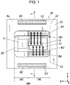
Fig. 1] Fig. 1 is a plan view of an electronic device according to an embodiment of the present disclosure. - [
Fig. 2] Fig. 2 is a sectional view, taken along a line A-A, of the electronic device illustrated inFig. 1 . - [
Fig. 3] Fig. 3 is a sectional view of the electronic device illustrated inFig. 1 , including an optical axis of the electronic device. - [
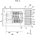
Fig. 4] Fig. 4 is a plan view of an electronic device according to a modification of the electronic device illustrated inFig. 1 . - [
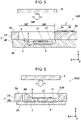
Fig. 5] Fig. 5 is a sectional view of the electronic device illustrated inFig. 4 , including an optical axis of the electronic device. - [
Fig. 6] Fig. 6 is a sectional view of an electronic device according to a modification of the electronic device illustrated inFig. 1 , including an optical axis of the electronic device. - [
Fig. 7] Fig. 7 is a sectional view of an electronic device according to a modification of the electronic device illustrated inFig. 4 , including an optical axis of the electronic device. - [
Fig. 8] Fig. 8 is a longitudinal sectional view of an exemplary electronic module according to the present disclosure. - [
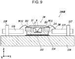
Fig. 9] Fig. 9 is a longitudinal sectional view of another exemplary electronic module according to the present disclosure. - Embodiments of the present disclosure are described in detail below with reference to the drawings.
- In the following description, "upper" or "top" refers to a direction toward a first surface Su of a
base 2, and "lower" or "bottom" refers to a direction toward a second surface Sb. Directional terms such as upper, top, bottom, or lower as used herein may not necessarily coincide with the upper, top, bottom, or lower side during actual use of anelectronic device 10. In the drawings, the Z-axis is depicted as the direction of thickness (top-bottom direction) of an optical-element mounting package, and the X-axis and the Y-axis are depicted as coordinate axes that are perpendicular to the Z-axis and orthogonal to each other. The X-axis coincides with the direction of the optical axis of anoptical element 11. - The
electronic device 10 according to Embodiment 1 includes: thebase 2 having the first surface Su, the second surface Sb, and acavity 3 defined in the first surface Su; theoptical element 11 and areflecting component 8, which are to be mounted within thecavity 3; and alid 9 that closes the top opening of thecavity 3. Thelid 9 is made of a material that transmits light (glass or resin). Thelid 9 is joined to the first surface Su of thebase 2 by use of a joining material. It is to be noted thatFig. 1 does not illustrate thelid 9, andFigs. 2 and 3 illustrate thelid 9 as being separated from the main body. A portion of theelectronic device 10 excluding thelid 9, theoptical element 11, and asub-mount 12 corresponds to an optical-element mounting package. - The
base 2 includes aninsulating base 2A and ametal base 2B. Theinsulating base 2A is located on themetal base 2B. Theinsulating base 2A is in the shape of a frame with a through-hole 3a that extends through theinsulating base 2A in the Z-direction. Themetal base 2B includes arecess 3b that communicates with the through-hole 3a. Theinsulating base 2A and themetal base 2B are to be joined together. Upon joining theinsulating base 2A and themetal base 2B together, the recess 3b and the through-hole 3a communicate with each other to define thecavity 3 that opens upward. In other words, thecavity 3 includes therecess 3b defined in themetal base 2B. - The
insulating base 2A is made of, for example, a ceramic material such as a sintered aluminum oxide compact (alumina ceramic), a sintered aluminum nitride compact, a sintered mullite compact, or a sintered glass-ceramic compact. Theinsulating base 2A can be fabricated by, for example, shaping a ceramic green sheet, which is a ceramic material that has not been sintered yet, into a predetermined shape by blanking, die cutting, or other methods, and sintering the resulting ceramic green sheet. Theinsulating base 2A further includes: external terminals D1 and D2 disposed on the first surface Su; and a wiring (V1, V2, L1, L2) electrically connected to each of the external terminals D1 and D2 to supply electricity from each of the external terminals D1 and D2 to theoptical element 11. The wiring includes vias V1 and V2 and wiring conductor layers L1 and L2. Each of the wiring conductor layers L1 and L2 has a portion located within theinsulating base 2A and a portion exposed into thecavity 3. The respective portions of the wiring conductor layers L1 and L2 that are exposed into thecavity 3 serve as internal connection pads D3 and D4. Each of the internal connection pads D3 and D4 is supported on the upper surface of astepped portion 14 provided inside theinsulating base 2A. The internal connection pads D3 and D4 are used as wire bonding pads. As described above, the wiring (V1, V2, L1, L2) provided in theinsulating base 2A is positioned to extend continuously through the interior of theinsulating base 2A into thecavity 3 from an outer surface (Su) of theinsulating base 2A on which each of the external terminals D1 and D2 is to be disposed. - The wiring (V1, V2, L1, L2) provided in the
insulating base 2A can be formed by coating or filling a predetermined portion of a ceramic green sheet with a conductor paste prior to sintering and then sintering the conductor paste together with the ceramic green sheet. - The
metal base 2B is made of, for example, a metallic material with high thermal conductivity, such as copper or aluminum. Themetal base 2B can be formed by, for example, press forming or other methods. Therecess 3b of themetal base 2B includes afirst mounting portion 4 where theoptical element 11 is to be mounted via thesub-mount 12 and asecond mounting portion 5 where the reflectingcomponent 8 is to be mounted. Thefirst mounting portion 4 defines, for example, a planar surface that extends horizontally. The term "planar" conceptually includes strictly planar surfaces as well as surfaces that can be regarded as planar if minute irregularities are ignored. Thesecond mounting portion 5 defines a planar surface inclined with respect to the horizontal direction. Thesecond mounting portion 5 is inclined such that thesecond mounting portion 5 increases in elevation with increasing distance from thefirst mounting portion 4. - The
optical element 11 is, for example, a laser diode (semiconductor laser). Theoptical element 11 may be any light-emitting element having directivity. Theoptical element 11 is joined to the upper surface of the sub-mount 12 by use of a joining material, and the sub-mount 12 is joined to the upper surface of the first mountingportion 4 by use of a joining material. The direction in which light is emitted by the optical element 11 (X-direction) coincides with a direction along the upper surface of the first mountingportion 4 or the upper surface of the sub-mount 12 (e.g., horizontal direction) and points toward the second mountingportion 5. Theoptical element 11 is electrically connected to the internal connection pads D3 and D4 via a wiring conductor provided in the sub-mount 12 and via bonding wires W1 and W2, respectively. The internal connection pads D3 and D4, which are located inside thecavity 3, are respectively electrically connected to the external terminals D1 and D2, which are located outside thecavity 3, via the wiring conductor (L1, L2, V1, V2). Theoptical element 11 is driven when electric power is input via the external terminals D1 and D2. - The reflecting
component 8 is a flat mirror. The reflectingcomponent 8 reflects incoming light from theoptical element 11 upward. The reflected light is directed to exit theelectronic device 10 upward via thelid 9. - As illustrated in
Figs. 1 and3 , thecavity 3, which is enclosed by themetal base 2B and the inner wall of the insulatingbase 2A, includes afirst region 301 and asecond region 302. Thefirst region 301 includes the first mountingportion 4 for theoptical element 11. Thesecond region 302 includes the second mountingportion 5 for the reflectingcomponent 8. Thefirst region 301 and thesecond region 302 are arranged in the X-direction in which light from theoptical element 11 travels toward the reflectingcomponent 8. The wiring (V1, V2, L1, L2) provided in the insulatingbase 2A is located toward thefirst region 301 relative to thesecond region 302. - The following describes Embodiment 1 in further detail.
- With the
cavity 3 viewed in plan as illustrated inFig. 1 , animaginary boundary line 300 is drawn that runs parallel to the Y-axis and divides the first mountingportion 4 and the second mountingportion 5 from each other. A region including the first mountingportion 4 is defined as thefirst region 301, and a region including the second mountingportion 5 is defined as thesecond region 302. - As for the wiring (V1, V2, L1, L2) provided in the insulating
base 2A, a portion of the wiring located inside thecavity 3 serves as the internal connection pads D3 and D4. - The internal connection pads D3 and D4 are located in the
first region 301. The sub-mount 12 and the bonding wires W1 and W2 are also located in thefirst region 301. - The wiring extending from the
optical element 11 to the external terminals D1 and D2 is not located in thesecond region 302. - Among major thermal conduction paths for heat generated from the
optical element 11 to themetal base 2B, a first path is a path along which heat is conducted from theoptical element 11 to the sub-mount 12 and then to themetal base 2B. A second path is a path along which heat is conducted from theoptical element 11 to the bonding wire W1 and then to the internal connection pad D3 and, after being conducted to the internal connection pad D3, the heat spreads across the entire wiring conductor layer L1 while being conducted to themetal base 2B via the insulation located under the wiring conductor layer L1. A third path is a path along which heat is conducted from theoptical element 11 to the sub-mount 12, the bonding wire W2, and then to the internal connection pad D4 and, after being conducted to the internal connection pad D4, the heat spreads across the entire wiring conductor layer L2 while being conducted to themetal base 2B via the insulation located under the wiring conductor layer L1. The entirety of each of the wiring conductor layers L1 and L2 is similarly located toward thefirst region 301 relative to theimaginary boundary line 300. - This helps to reduce conduction of heat generated in the
optical element 11 toward the reflectingcomponent 8, which consequently reduces potential deformation of the reflectingcomponent 8 caused by heat. This leads to stable optical characteristics. - According to Embodiment 1, the internal connection pads D3 and D4 are located in a direction (Y-direction) perpendicular to the direction of arrangement of the
first region 301 and the second region 302 (X-direction) and passing through the first mountingportion 4. In other words, the internal connection pad D3 is adjacent to the first mountingportion 4 in the Y-direction. Likewise, the internal connection pad D4 is adjacent to the first mountingportion 4 in the Y-direction. - This allows the internal connection pads D3 and D4 to be increased in length in the X-direction. Furthermore, the bonding wires W1 and W2 extend in the Y-direction. It is therefore easy to increase the number of bonding wires W1 that can be arranged side by side as illustrated in
Fig. 1 . Further, it is easy to increase the number of bonding wires W2 that can be arranged side by side. - The ability to increase the number of bonding wires W1 and W2 that can be arranged side by side allows for reduced electrical resistance at the location of the bonding wires W1 and W2 and improved thermal conductivity. This makes it possible to increase the amount of thermal conduction along the second and third paths, resulting in improved thermal conduction to the
metal base 2B. - This helps to reduce conduction of heat generated in the
optical element 11 toward the reflectingcomponent 8, which consequently reduces potential deformation of the reflectingcomponent 8 caused by heat. This leads to stable optical characteristics. - According to Embodiment 1, the
cavity 3 has a rectangular shape in plan view as illustrated inFig. 1 . The long side of thecavity 3 extends in the X-direction, and the short side extends in the Y-direction. In other words, the longitudinal direction of thecavity 3 coincides with the X-direction in which thefirst region 301 and thesecond region 302 are arranged. - This allows the
first region 301 to have a sufficient dimension in the X-direction for placement of theoptical element 11 that is elongated in the direction of the optical axis (X-direction). The increased dimension of thefirst region 301 in the X-direction makes it easy to increase the length of the sub-mount 12 in the X-direction and to increase the length of each of the internal connection pads D3 and D4 in the X-direction. - It is therefore easy to increase the number of bonding wires W1 and W2 that can be arranged side by side.
- According to Embodiment 1, the dimension of the
first region 301 in the X-direction is made larger than the dimension of thesecond region 302 in the X-direction. This helps to ensure a sufficient dimension in the X-axis direction for placement of theoptical element 11 and also makes it easy to increase the length of the sub-mount 12 in the X-direction and to increase the length of each of the internal connection pads D3 and D4 in the X-direction. It is therefore easy to increase the number of bonding wires W1 and W2 that can be arranged side by side. - Implementing the above-mentioned configuration together with forming the
cavity 3 as a rectangle elongated in the X-direction as described above makes it easier to increase the number of bonding wires W1 and W2 that can be arranged side by side. - As viewed in the Z-direction, the external terminals D1 and D2 are located at a position on the insulating
base 2A where the external terminals D1 and D2 at least partially overlap themetal base 2B. - This helps to ensure that heat conducted to the external terminals D1 and D2 and further to the vias V1 and V2 respectively located under the external terminals D1 and D2 is readily conducted in the Z-direction and absorbed by the
metal base 2B. - This helps to reduce conduction of heat generated in the
optical element 11 toward the reflectingcomponent 8, which consequently reduces potential deformation of the reflectingcomponent 8 caused by heat. This leads to stable optical characteristics. - According to Embodiment 1, the external terminals D1 and D2 are located in the Y-direction passing through the first mounting
portion 4 and perpendicular to the X-direction in which thefirst region 301 and thesecond region 302 are arranged. - This helps to reduce an increase in the overall size of the package in the X-direction, which allows for miniaturization of the package.
-
Embodiment 2 representing a modification of Embodiment 1 mentioned above is illustrated in each ofFigs. 4 and5 . - According to Embodiment 1 mentioned above, the external terminals D1 and D2 are located in the Y-direction passing through the first mounting
portion 4 and perpendicular to the X-direction in which thefirst region 301 and thesecond region 302 are arranged. - As opposed to Embodiment 1, for an optical-element mounting package according to
Embodiment 2 and anelectronic device 10B using the optical-element mounting package according toEmbodiment 2, the external terminals D1 and D2 are located on the opposite side across the first mountingportion 4 from the second mountingportion 5. - The above-mentioned configuration results in increased length of the wiring conductor layers L1 and L2.
- Heat that is generated in the
optical element 11 and to be conducted through the wiring conductor layers L1 and L2 is conducted away in the X-direction from thesecond region 302 where the reflectingcomponent 8 is located. - This helps to reduce conduction of heat generated in the
optical element 11 toward the reflectingcomponent 8, which consequently reduces potential deformation of the reflectingcomponent 8 caused by heat. This leads to stable optical characteristics. - In comparison to Embodiment 1 mentioned above,
Embodiment 2 results in increased dimension in the X-direction but allows for reduced dimension in the Y-direction. -
Embodiment 3 representing a modification ofEmbodiment 1 or 2 mentioned above is illustrated in each ofFigs. 6 and7 . - According to
Embodiments 1 and 2 mentioned above, the reflectingcomponent 8 is a flat mirror. Alternatively, as with an optical-element mounting package illustrated in each ofFigs. 6 and7 and electronic devices 10A1 (Fig. 6 ) and 10B1 (Fig. 7 ) that use the optical-element mounting package illustrated in each ofFigs. 6 and7 , aprism 8B may be used. - According to
Embodiments 1 and 2 mentioned above, themetal base 2B is provided with therecess 3b. In this regard, as with the optical-element mounting package illustrated in each ofFigs. 6 and7 and the electronic devices 10A1 (Fig. 6 ) and 10B1 (Fig. 7 ) that use the optical-element mounting package illustrated in each ofFigs. 6 and7 , an alternative configuration may be employed as described below. According to this configuration, a flat-shaped metal base 2B1 is used, and the internal space of thecavity 3 is defined only by the through-hole 3a of the insulatingbase 2A. - Using the
prism 8B in combination with the flat-shaped metal base 2B1 helps to ensure that even if the second mountingportion 5 on which theprism 8B is to be mounted is an X-Y plane, the reflecting surface of theprism 8B that reflects incoming light from theoptical element 11 can be easily inclined with respect to the X-Y plane. -
Fig. 8 is a longitudinal sectional view of an exemplary electronic module.Fig. 9 is a longitudinal sectional view of another exemplary electronic module. - An
electronic module 100A inFig. 8 includes theelectronic device 10 mounted over amodule substrate 110. Alternatively, theelectronic device 10B, 10A1, or 10B1 according to each of the modifications mentioned above may be mounted. In addition to theelectronic device 10, other components such as another electronic device, an electronic element, and an electrical element may be mounted over themodule substrate 110. Themodule substrate 110 is provided withelectrode pads electronic device 10 is joined to theelectrode pad 111 via a joiningmaterial 114 such as solder. More specifically, the lower surface (second surface Sb) of themetal base 2B is joined to theelectrode pad 111 via the joiningmaterial 114 such as solder. The external terminals D1 and D2 of theelectronic device 10 may be respectively connected to theelectrode pads module substrate 110 via bonding wires W11 and W12. A signal may be output from themodule substrate 110 to theelectronic device 10 via theelectrode pads module substrate 110 and via the bonding wires W11 and W12. - In an
electronic module 100B illustrated inFig. 9 , the external terminals D1 and D2 of theelectronic device 10 are respectively connected to leadpins module substrate 110 via the bonding wires W11 and W12. The lead pins 115 and 116 are electrode terminals respectively supported to themodule substrate 110 by lead-pin supports 117 and 118. A signal may be output from themodule substrate 110 to theelectronic device 10 via the lead pins 115 and 116 of themodule substrate 110 and via the bonding wires W11 and W12. - As described above, with the
electronic module - Embodiments of the present disclosure have been described above. These embodiments, however, are not intended to limit the present invention. For example, the details illustrated in the embodiments and the drawings, such as the materials, shapes, and sizes of various portions of the bases or optical components may be modified or altered as appropriate without departing from the scope and spirit of the invention.
- The present disclosure can find utility as an optical-element mounting package, an electronic device, and an electronic module.
-
- 2 base
- 2A insulating base
- 2B metal base
- 3 cavity
- 3a through-hole
- 3b recess
- 4 first mounting portion
- 5 second mounting portion
- 8 reflecting component
- 9 lid
- 10 electronic device
- 11 optical element
- 12 sub-mount
- 100A, 100B electronic module
- 110 module substrate
- 111, 112, 113 electrode pad
- 114 joining material
- 115, 116 lead pin
- 117, 118 lead-pin support
- D1, D2 external terminal
- D3, D4 internal connection pad
- L1, L2 wiring conductor layer
- V1, V2 via
- W1, W2 bonding wire
- W11, W12 bonding wire
- 301 first region
- 302 second region
Claims (10)
- An optical-element mounting package comprising:a metal base;an insulating base having a frame shape and located on the metal base;an external terminal located on the insulating base;a wiring located in the insulating base and electrically connected to the external terminal; anda reflecting component,wherein a cavity enclosed by the metal base and an inner wall of the insulating base includes a first region and a second region,wherein the first region includes a first mounting portion for an optical element,wherein the second region includes a second mounting portion for the reflecting component,wherein the first region and the second region are arranged in a direction in which light from the optical element travels toward the reflecting component, andwherein the wiring is located toward the first region relative to the second region.
- The optical-element mounting package according to Claim 1, wherein in plan view, the wiring is located in a direction perpendicular to a direction of arrangement of the first region and the second region and passing through the first mounting portion.
- The optical-element mounting package according to Claim 1 or 2, wherein the external terminal is located at a position where the external terminal at least partially overlaps the metal base.
- The optical-element mounting package according to any one of Claims 1 to 3, wherein a longitudinal direction of the cavity coincides with a direction of arrangement of the first region and the second region.
- The optical-element mounting package according to any one of Claims 1 to 4, wherein in plan view, the external terminal is located in a direction perpendicular to a direction of arrangement of the first region and the second region and passing through the first mounting portion.
- The optical-element mounting package according to any one of Claims 1 to 5, wherein the external terminal is located on an opposite side across the first mounting portion from the second mounting portion.
- The optical-element mounting package according to any one of Claims 1 to 6, wherein the cavity includes a recess defined in the metal base.
- The optical-element mounting package according to any one of Claims 1 to 7, wherein the wiring is positioned to extend continuously through an interior of the insulating base into the cavity from an outer surface of the insulating base on which the external terminal is to be disposed.
- An electronic device comprising:the optical-element mounting package according to any one of Claims 1 to 8; andan optical element mounted over the first mounting portion.
- An electronic module comprising:the electronic device according to Claim 9; anda module substrate over which the electronic device is mounted.
Applications Claiming Priority (2)
| Application Number | Priority Date | Filing Date | Title |
|---|---|---|---|
| JP2019147778 | 2019-08-09 | ||
| PCT/JP2020/030410 WO2021029371A1 (en) | 2019-08-09 | 2020-08-07 | Package for mounting optical element, electronic device, and electronic module |
Publications (2)
| Publication Number | Publication Date |
|---|---|
| EP4012760A1 true EP4012760A1 (en) | 2022-06-15 |
| EP4012760A4 EP4012760A4 (en) | 2023-10-25 |
Family
ID=74569685
Family Applications (1)
| Application Number | Title | Priority Date | Filing Date |
|---|---|---|---|
| EP20851554.4A Pending EP4012760A4 (en) | 2019-08-09 | 2020-08-07 | OPTICAL ELEMENT MOUNTING BOX, ELECTRONIC DEVICE AND ELECTRONIC MODULE |
Country Status (5)
| Country | Link |
|---|---|
| US (1) | US20220320823A1 (en) |
| EP (1) | EP4012760A4 (en) |
| JP (1) | JP7449295B2 (en) |
| CN (1) | CN114270641A (en) |
| WO (1) | WO2021029371A1 (en) |
Families Citing this family (1)
| Publication number | Priority date | Publication date | Assignee | Title |
|---|---|---|---|---|
| JP6711333B2 (en) | 2017-08-16 | 2020-06-17 | 日亜化学工業株式会社 | Light emitting device |
Family Cites Families (19)
| Publication number | Priority date | Publication date | Assignee | Title |
|---|---|---|---|---|
| US5327443A (en) * | 1991-10-30 | 1994-07-05 | Rohm Co., Ltd. | Package-type semiconductor laser device |
| US5748658A (en) * | 1993-10-22 | 1998-05-05 | Matsushita Electric Industrial Co., Ltd. | Semiconductor laser device and optical pickup head |
| JPH11176003A (en) * | 1997-12-09 | 1999-07-02 | Sony Corp | Optical composite element |
| JP4113442B2 (en) | 2002-05-09 | 2008-07-09 | ローム株式会社 | Semiconductor laser, manufacturing method thereof, and optical pickup device |
| JP2005038956A (en) * | 2003-07-17 | 2005-02-10 | Matsushita Electric Ind Co Ltd | Optical component and manufacturing method thereof |
| US7550319B2 (en) * | 2005-09-01 | 2009-06-23 | E. I. Du Pont De Nemours And Company | Low temperature co-fired ceramic (LTCC) tape compositions, light emitting diode (LED) modules, lighting devices and method of forming thereof |
| JP5812671B2 (en) * | 2011-04-28 | 2015-11-17 | 京セラ株式会社 | Device storage package and semiconductor device including the same |
| JP2015185622A (en) * | 2014-03-22 | 2015-10-22 | 京セラ株式会社 | Electronic element mounting substrate and electronic device |
| WO2016171103A1 (en) * | 2015-04-24 | 2016-10-27 | 京セラ株式会社 | Package for mounting optical element, electronic device, and electronic module |
| CN112503404B (en) * | 2015-05-20 | 2023-03-28 | 日亚化学工业株式会社 | Light emitting device |
| JP6747799B2 (en) * | 2015-11-27 | 2020-08-26 | 京セラ株式会社 | Optical element mounting package, optical element mounting mother board, and electronic device |
| US10122146B2 (en) * | 2016-04-05 | 2018-11-06 | Aquifi, Inc. | Thin laser package for optical applications |
| RU2019106302A (en) * | 2016-08-10 | 2020-09-16 | Киосера Корпорейшн | ELECTRIC ELEMENT MOUNTING HOUSING, MATRIX HOUSING AND ELECTRICAL DEVICE |
| JP6893781B2 (en) * | 2016-12-20 | 2021-06-23 | 京セラ株式会社 | Light emitting element mounting package and light emitting device |
| JP6880725B2 (en) * | 2016-12-27 | 2021-06-02 | 日亜化学工業株式会社 | Light emitting device |
| JP6940750B2 (en) * | 2017-04-28 | 2021-09-29 | 日亜化学工業株式会社 | Laser device |
| JP6711333B2 (en) * | 2017-08-16 | 2020-06-17 | 日亜化学工業株式会社 | Light emitting device |
| JP2019047072A (en) * | 2017-09-07 | 2019-03-22 | 株式会社アマダホールディングス | Laser light source module, manufacturing method of laser light source module, and laser light source module unit |
| US11309680B2 (en) * | 2017-09-28 | 2022-04-19 | Nichia Corporation | Light source device including lead terminals that cross space defined by base and cap |
-
2020
- 2020-08-07 JP JP2021539279A patent/JP7449295B2/en active Active
- 2020-08-07 EP EP20851554.4A patent/EP4012760A4/en active Pending
- 2020-08-07 CN CN202080055985.1A patent/CN114270641A/en active Pending
- 2020-08-07 WO PCT/JP2020/030410 patent/WO2021029371A1/en not_active Ceased
- 2020-08-07 US US17/633,606 patent/US20220320823A1/en not_active Abandoned
Also Published As
| Publication number | Publication date |
|---|---|
| US20220320823A1 (en) | 2022-10-06 |
| CN114270641A (en) | 2022-04-01 |
| JP7449295B2 (en) | 2024-03-13 |
| EP4012760A4 (en) | 2023-10-25 |
| JPWO2021029371A1 (en) | 2021-02-18 |
| WO2021029371A1 (en) | 2021-02-18 |
Similar Documents
| Publication | Publication Date | Title |
|---|---|---|
| US8198108B2 (en) | Semiconductor device and method for manufacturing the same | |
| KR101513961B1 (en) | Power semiconductor module and method of manufacturing the same | |
| US10333037B2 (en) | Light-emitting-element mounting package and method for manufacturing the same | |
| JP2008270302A (en) | Semiconductor device | |
| KR20030024157A (en) | Power semiconductor module that has three dimensional structure and a method of manufacturing thereof | |
| US20250183615A1 (en) | Optical element mounting package, electronic device, and electronic module | |
| IT202000032267A1 (en) | ENCAPSULATED ELECTRONIC DEVICE WITH HIGH THERMAL DISSIPATION AND RELATED MANUFACTURING PROCEDURE | |
| EP4012760A1 (en) | Package for mounting optical element, electronic device, and electronic module | |
| US12164175B2 (en) | Mounting package for an optical element with inclined transmission film and flat mirror | |
| US20240213433A1 (en) | Substrate, package, electronic component, and light emitting device | |
| CN114530757A (en) | Optical semiconductor module | |
| JP2024111284A (en) | Electronics | |
| US11955769B2 (en) | Optical element mounting package, electronic device, and electronic module | |
| US11778747B2 (en) | Wiring board, composite substrate, and electric device | |
| JP7399180B2 (en) | Packages for mounting optical elements, electronic devices, and electronic modules | |
| CN115864122A (en) | Light-emitting device, light-emitting device manufacturing method and light source module | |
| WO2020175619A1 (en) | Electronic component mounting package, electronic device, and light-emitting device | |
| JPH09121018A (en) | Semiconductor device | |
| CN219497790U (en) | Package element | |
| TW202407911A (en) | Electronic component package and the manufacturing method thereof | |
| CN120432988A (en) | Light-emitting device and display device | |
| CN120545794A (en) | Edge laser package | |
| CN116888727A (en) | Semiconductor packages and semiconductor electronic devices | |
| JP2019207992A (en) | Package for mounting electrical element and electrical apparatus | |
| JP2003332635A (en) | Thermoelectric conversion element module |
Legal Events
| Date | Code | Title | Description |
|---|---|---|---|
| STAA | Information on the status of an ep patent application or granted ep patent |
Free format text: STATUS: THE INTERNATIONAL PUBLICATION HAS BEEN MADE |
|
| PUAI | Public reference made under article 153(3) epc to a published international application that has entered the european phase |
Free format text: ORIGINAL CODE: 0009012 |
|
| STAA | Information on the status of an ep patent application or granted ep patent |
Free format text: STATUS: REQUEST FOR EXAMINATION WAS MADE |
|
| 17P | Request for examination filed |
Effective date: 20220204 |
|
| AK | Designated contracting states |
Kind code of ref document: A1 Designated state(s): AL AT BE BG CH CY CZ DE DK EE ES FI FR GB GR HR HU IE IS IT LI LT LU LV MC MK MT NL NO PL PT RO RS SE SI SK SM TR |
|
| DAV | Request for validation of the european patent (deleted) | ||
| DAX | Request for extension of the european patent (deleted) | ||
| P01 | Opt-out of the competence of the unified patent court (upc) registered |
Effective date: 20230505 |
|
| A4 | Supplementary search report drawn up and despatched |
Effective date: 20230922 |
|
| RIC1 | Information provided on ipc code assigned before grant |
Ipc: H01S 5/02345 20210101ALI20230918BHEP Ipc: H01S 5/02255 20210101ALI20230918BHEP Ipc: H01S 5/022 20210101ALI20230918BHEP Ipc: H01L 23/02 20060101AFI20230918BHEP |