EP4012756A1 - Substrate processing system and substrate processing method - Google Patents
Substrate processing system and substrate processing method Download PDFInfo
- Publication number
- EP4012756A1 EP4012756A1 EP20849250.4A EP20849250A EP4012756A1 EP 4012756 A1 EP4012756 A1 EP 4012756A1 EP 20849250 A EP20849250 A EP 20849250A EP 4012756 A1 EP4012756 A1 EP 4012756A1
- Authority
- EP
- European Patent Office
- Prior art keywords
- substrate
- transfer
- modules
- aligner
- module
- Prior art date
- Legal status (The legal status is an assumption and is not a legal conclusion. Google has not performed a legal analysis and makes no representation as to the accuracy of the status listed.)
- Pending
Links
Images


Classifications
-
- C—CHEMISTRY; METALLURGY
- C23—COATING METALLIC MATERIAL; COATING MATERIAL WITH METALLIC MATERIAL; CHEMICAL SURFACE TREATMENT; DIFFUSION TREATMENT OF METALLIC MATERIAL; COATING BY VACUUM EVAPORATION, BY SPUTTERING, BY ION IMPLANTATION OR BY CHEMICAL VAPOUR DEPOSITION, IN GENERAL; INHIBITING CORROSION OF METALLIC MATERIAL OR INCRUSTATION IN GENERAL
- C23C—COATING METALLIC MATERIAL; COATING MATERIAL WITH METALLIC MATERIAL; SURFACE TREATMENT OF METALLIC MATERIAL BY DIFFUSION INTO THE SURFACE, BY CHEMICAL CONVERSION OR SUBSTITUTION; COATING BY VACUUM EVAPORATION, BY SPUTTERING, BY ION IMPLANTATION OR BY CHEMICAL VAPOUR DEPOSITION, IN GENERAL
- C23C14/00—Coating by vacuum evaporation, by sputtering or by ion implantation of the coating forming material
- C23C14/22—Coating by vacuum evaporation, by sputtering or by ion implantation of the coating forming material characterised by the process of coating
- C23C14/56—Apparatus specially adapted for continuous coating; Arrangements for maintaining the vacuum, e.g. vacuum locks
- C23C14/568—Transferring the substrates through a series of coating stations
-
- C—CHEMISTRY; METALLURGY
- C23—COATING METALLIC MATERIAL; COATING MATERIAL WITH METALLIC MATERIAL; CHEMICAL SURFACE TREATMENT; DIFFUSION TREATMENT OF METALLIC MATERIAL; COATING BY VACUUM EVAPORATION, BY SPUTTERING, BY ION IMPLANTATION OR BY CHEMICAL VAPOUR DEPOSITION, IN GENERAL; INHIBITING CORROSION OF METALLIC MATERIAL OR INCRUSTATION IN GENERAL
- C23C—COATING METALLIC MATERIAL; COATING MATERIAL WITH METALLIC MATERIAL; SURFACE TREATMENT OF METALLIC MATERIAL BY DIFFUSION INTO THE SURFACE, BY CHEMICAL CONVERSION OR SUBSTITUTION; COATING BY VACUUM EVAPORATION, BY SPUTTERING, BY ION IMPLANTATION OR BY CHEMICAL VAPOUR DEPOSITION, IN GENERAL
- C23C14/00—Coating by vacuum evaporation, by sputtering or by ion implantation of the coating forming material
- C23C14/06—Coating by vacuum evaporation, by sputtering or by ion implantation of the coating forming material characterised by the coating material
-
- C—CHEMISTRY; METALLURGY
- C23—COATING METALLIC MATERIAL; COATING MATERIAL WITH METALLIC MATERIAL; CHEMICAL SURFACE TREATMENT; DIFFUSION TREATMENT OF METALLIC MATERIAL; COATING BY VACUUM EVAPORATION, BY SPUTTERING, BY ION IMPLANTATION OR BY CHEMICAL VAPOUR DEPOSITION, IN GENERAL; INHIBITING CORROSION OF METALLIC MATERIAL OR INCRUSTATION IN GENERAL
- C23C—COATING METALLIC MATERIAL; COATING MATERIAL WITH METALLIC MATERIAL; SURFACE TREATMENT OF METALLIC MATERIAL BY DIFFUSION INTO THE SURFACE, BY CHEMICAL CONVERSION OR SUBSTITUTION; COATING BY VACUUM EVAPORATION, BY SPUTTERING, BY ION IMPLANTATION OR BY CHEMICAL VAPOUR DEPOSITION, IN GENERAL
- C23C14/00—Coating by vacuum evaporation, by sputtering or by ion implantation of the coating forming material
- C23C14/22—Coating by vacuum evaporation, by sputtering or by ion implantation of the coating forming material characterised by the process of coating
- C23C14/34—Sputtering
- C23C14/35—Sputtering by application of a magnetic field, e.g. magnetron sputtering
- C23C14/351—Sputtering by application of a magnetic field, e.g. magnetron sputtering using a magnetic field in close vicinity to the substrate
-
- C—CHEMISTRY; METALLURGY
- C23—COATING METALLIC MATERIAL; COATING MATERIAL WITH METALLIC MATERIAL; CHEMICAL SURFACE TREATMENT; DIFFUSION TREATMENT OF METALLIC MATERIAL; COATING BY VACUUM EVAPORATION, BY SPUTTERING, BY ION IMPLANTATION OR BY CHEMICAL VAPOUR DEPOSITION, IN GENERAL; INHIBITING CORROSION OF METALLIC MATERIAL OR INCRUSTATION IN GENERAL
- C23C—COATING METALLIC MATERIAL; COATING MATERIAL WITH METALLIC MATERIAL; SURFACE TREATMENT OF METALLIC MATERIAL BY DIFFUSION INTO THE SURFACE, BY CHEMICAL CONVERSION OR SUBSTITUTION; COATING BY VACUUM EVAPORATION, BY SPUTTERING, BY ION IMPLANTATION OR BY CHEMICAL VAPOUR DEPOSITION, IN GENERAL
- C23C14/00—Coating by vacuum evaporation, by sputtering or by ion implantation of the coating forming material
- C23C14/22—Coating by vacuum evaporation, by sputtering or by ion implantation of the coating forming material characterised by the process of coating
- C23C14/50—Substrate holders
-
- C—CHEMISTRY; METALLURGY
- C23—COATING METALLIC MATERIAL; COATING MATERIAL WITH METALLIC MATERIAL; CHEMICAL SURFACE TREATMENT; DIFFUSION TREATMENT OF METALLIC MATERIAL; COATING BY VACUUM EVAPORATION, BY SPUTTERING, BY ION IMPLANTATION OR BY CHEMICAL VAPOUR DEPOSITION, IN GENERAL; INHIBITING CORROSION OF METALLIC MATERIAL OR INCRUSTATION IN GENERAL
- C23C—COATING METALLIC MATERIAL; COATING MATERIAL WITH METALLIC MATERIAL; SURFACE TREATMENT OF METALLIC MATERIAL BY DIFFUSION INTO THE SURFACE, BY CHEMICAL CONVERSION OR SUBSTITUTION; COATING BY VACUUM EVAPORATION, BY SPUTTERING, BY ION IMPLANTATION OR BY CHEMICAL VAPOUR DEPOSITION, IN GENERAL
- C23C14/00—Coating by vacuum evaporation, by sputtering or by ion implantation of the coating forming material
- C23C14/22—Coating by vacuum evaporation, by sputtering or by ion implantation of the coating forming material characterised by the process of coating
- C23C14/50—Substrate holders
- C23C14/505—Substrate holders for rotation of the substrates
-
- G—PHYSICS
- G11—INFORMATION STORAGE
- G11B—INFORMATION STORAGE BASED ON RELATIVE MOVEMENT BETWEEN RECORD CARRIER AND TRANSDUCER
- G11B5/00—Recording by magnetisation or demagnetisation of a record carrier; Reproducing by magnetic means; Record carriers therefor
- G11B5/84—Processes or apparatus specially adapted for manufacturing record carriers
- G11B5/85—Coating a support with a magnetic layer by vapour deposition
-
- H—ELECTRICITY
- H01—ELECTRIC ELEMENTS
- H01J—ELECTRIC DISCHARGE TUBES OR DISCHARGE LAMPS
- H01J37/00—Discharge tubes with provision for introducing objects or material to be exposed to the discharge, e.g. for the purpose of examination or processing thereof
- H01J37/32—Gas-filled discharge tubes
- H01J37/32431—Constructional details of the reactor
- H01J37/32733—Means for moving the material to be treated
-
- H—ELECTRICITY
- H01—ELECTRIC ELEMENTS
- H01J—ELECTRIC DISCHARGE TUBES OR DISCHARGE LAMPS
- H01J37/00—Discharge tubes with provision for introducing objects or material to be exposed to the discharge, e.g. for the purpose of examination or processing thereof
- H01J37/32—Gas-filled discharge tubes
- H01J37/32431—Constructional details of the reactor
- H01J37/32733—Means for moving the material to be treated
- H01J37/32743—Means for moving the material to be treated for introducing the material into processing chamber
-
- H—ELECTRICITY
- H01—ELECTRIC ELEMENTS
- H01J—ELECTRIC DISCHARGE TUBES OR DISCHARGE LAMPS
- H01J37/00—Discharge tubes with provision for introducing objects or material to be exposed to the discharge, e.g. for the purpose of examination or processing thereof
- H01J37/32—Gas-filled discharge tubes
- H01J37/32431—Constructional details of the reactor
- H01J37/32733—Means for moving the material to be treated
- H01J37/32788—Means for moving the material to be treated for extracting the material from the process chamber
-
- H—ELECTRICITY
- H01—ELECTRIC ELEMENTS
- H01J—ELECTRIC DISCHARGE TUBES OR DISCHARGE LAMPS
- H01J37/00—Discharge tubes with provision for introducing objects or material to be exposed to the discharge, e.g. for the purpose of examination or processing thereof
- H01J37/32—Gas-filled discharge tubes
- H01J37/32431—Constructional details of the reactor
- H01J37/32798—Further details of plasma apparatus not provided for in groups H01J37/3244 - H01J37/32788; special provisions for cleaning or maintenance of the apparatus
- H01J37/32889—Connection or combination with other apparatus
-
- H—ELECTRICITY
- H01—ELECTRIC ELEMENTS
- H01J—ELECTRIC DISCHARGE TUBES OR DISCHARGE LAMPS
- H01J37/00—Discharge tubes with provision for introducing objects or material to be exposed to the discharge, e.g. for the purpose of examination or processing thereof
- H01J37/32—Gas-filled discharge tubes
- H01J37/32431—Constructional details of the reactor
- H01J37/32798—Further details of plasma apparatus not provided for in groups H01J37/3244 - H01J37/32788; special provisions for cleaning or maintenance of the apparatus
- H01J37/32899—Multiple chambers, e.g. cluster tools
-
- H—ELECTRICITY
- H01—ELECTRIC ELEMENTS
- H01J—ELECTRIC DISCHARGE TUBES OR DISCHARGE LAMPS
- H01J37/00—Discharge tubes with provision for introducing objects or material to be exposed to the discharge, e.g. for the purpose of examination or processing thereof
- H01J37/32—Gas-filled discharge tubes
- H01J37/34—Gas-filled discharge tubes operating with cathodic sputtering
- H01J37/3411—Constructional aspects of the reactor
- H01J37/345—Magnet arrangements in particular for cathodic sputtering apparatus
- H01J37/3452—Magnet distribution
-
- H—ELECTRICITY
- H10—SEMICONDUCTOR DEVICES; ELECTRIC SOLID-STATE DEVICES NOT OTHERWISE PROVIDED FOR
- H10P—GENERIC PROCESSES OR APPARATUS FOR THE MANUFACTURE OR TREATMENT OF DEVICES COVERED BY CLASS H10
- H10P72/00—Handling or holding of wafers, substrates or devices during manufacture or treatment thereof
- H10P72/04—Apparatus for manufacture or treatment
- H10P72/0451—Apparatus for manufacturing or treating in a plurality of work-stations
- H10P72/0461—Apparatus for manufacturing or treating in a plurality of work-stations characterised by the presence of two or more transfer chambers
-
- H—ELECTRICITY
- H10—SEMICONDUCTOR DEVICES; ELECTRIC SOLID-STATE DEVICES NOT OTHERWISE PROVIDED FOR
- H10P—GENERIC PROCESSES OR APPARATUS FOR THE MANUFACTURE OR TREATMENT OF DEVICES COVERED BY CLASS H10
- H10P72/00—Handling or holding of wafers, substrates or devices during manufacture or treatment thereof
- H10P72/30—Handling or holding of wafers, substrates or devices during manufacture or treatment thereof for conveying, e.g. between different workstations
- H10P72/33—Handling or holding of wafers, substrates or devices during manufacture or treatment thereof for conveying, e.g. between different workstations into and out of processing chamber
- H10P72/3302—Mechanical parts of transfer devices
-
- B—PERFORMING OPERATIONS; TRANSPORTING
- B82—NANOTECHNOLOGY
- B82Y—SPECIFIC USES OR APPLICATIONS OF NANOSTRUCTURES; MEASUREMENT OR ANALYSIS OF NANOSTRUCTURES; MANUFACTURE OR TREATMENT OF NANOSTRUCTURES
- B82Y10/00—Nanotechnology for information processing, storage or transmission, e.g. quantum computing or single electron logic
Definitions
- the present disclosure relates to a substrate processing system and a substrate processing method.
- a processing apparatus for performing a plurality of processes on a substrate
- a processing apparatus including a transfer part in which multiple transfer modules, each having a substrate transfer device, are arranged in one row and a plurality of process modules arranged on both sides of transfer chambers and configured to transfer substrates sequentially and serially in a U shape and perform a series of processes (see, e.g., Patent Document 1).
- the present disclosure provides a substrate processing system and a substrate processing method capable of maintaining a high productivity even when a substrate is aligned whenever the substrate is transferred to each of a plurality of process modules connected to a plurality of transfer modules in the case of serially transferring a plurality of substrates to the process modules and processing them.
- a substrate processing system including a plurality of transfer modules having transfer mechanisms for transferring substrates, and a plurality of process modules connected to the plurality of transfer modules.
- the transfer mechanisms of the plurality of transfer modules transfer a plurality of substrates sequentially and serially to the plurality of process modules.
- Each of the plurality of transfer modules has an aligner for aligning a substrate when transferring the same to the process module connected to the relevant transfer module.
- a substrate processing system and a substrate processing method capable of maintaining a high productivity even when a substrate is aligned whenever the substrate is transferred to each of a plurality of process modules connected to a plurality of transfer modules in the case of serially transferring a plurality of substrates to the process modules and processing them.
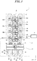
- Fig. 1 is a plan view schematically showing a substrate processing system according to the first embodiment.
- the substrate processing system 1 performs a plurality of processes on a substrate, and includes a processing part 2, a loading/unloading part 3 for holding a plurality of substrates and loading/unloading a substrate to/from the processing part 2, and a controller 4.
- the substrate is not particularly limited, but is a semiconductor wafer (hereinafter, simply referred to as "wafer”), for example.
- the processing part 2 includes a plurality of (eight in this example) process modules PM1 to PM8 for performing predetermined vacuum processing on substrates W, and a transfer part 12 having a plurality of transfer modules TM1 to TM4 for sequentially transferring substrates W to the process modules PM1 to PM8.
- the transfer modules TM1, TM2, TM3, and TM4 have containers 30a, 30b, 30c, 30d having a hexagonal planar shape and maintained in a vacuum state, and transfer mechanisms 31a, 31b, 31c, and 31d disposed in the containers, respectively. Delivery parts 41, 42, and 43 as transfer buffers are disposed between the transfer mechanisms of the transfer modules TM1 and TM2, between the transfer mechanisms of the transfer modules TM2 and TM3, and between the transfer mechanisms of the transfer modules TM3 and TM4, respectively.
- the containers 30a, 30b, 30c, and 30d of the transfer modules TM1 to TM4 communicate with each other.
- the transfer modules TM1 to TM4 are arranged in one row in the Y direction in the drawing, and four of the process modules PM1 to PM8 are connected to each of two sides of the transfer part 12 through gate valves G that can be opened and closed.
- the gate valves G of the process modules PM1 to PM8 are opened when the transfer mechanism of the transfer module accesses the process modules, and are closed during processing.
- the loading/unloading part 3 is connected to one end of the processing part 2.
- the loading/unloading part 3 includes an atmospheric transfer chamber (EFEM) 21, three load ports 22 connected to the atmospheric transfer chamber 21, two load-lock modules LLM1 and LLM2, and a transfer device 24 disposed in the atmospheric transfer chamber 21.
- EFEM atmospheric transfer chamber
- LLM1 and LLM2 load-lock modules
- the atmosphere transfer chamber 21 has a rectangular parallelepiped shape with the X direction as a longitudinal direction in the drawing.
- the three load ports 22 are disposed at a long sidewall of the atmospheric transfer chamber 21 opposite to a sidewall facing the processing part 2.
- Each load port 22 has a placement table 25 and a transfer port 26.
- a front opening unified pod (FOUP) 20 that is a wafer storage container accommodating a plurality of wafers is placed on the placement table 25, and the FOUP 20 on the placement table 25 is connected in a sealed state to the atmospheric transfer chamber 21 through the transfer port 26.
- FOUP front opening unified pod
- the two load-lock modules LLM1 and LLM2 allow wafers W to be transferred between the atmospheric transfer chamber 21 maintained at an atmospheric pressure and the transfer part 12 maintained at a vacuum atmosphere, and a pressure in each of the load-lock modules LLM1 and LLM2 is variable between an atmospheric pressure and a vacuum level similar to that in the transfer part 12.
- Each of the two load-lock modules LLM1 and LLM2 has two transfer ports. One of the two transfer ports is connected to the long sidewall of the atmospheric transfer chamber 21 facing the processing part 2 through a gate valve G2. The other transfer port is connected to the transfer part 12 of the processing part 2 through the gate valve G1.
- the load-lock module LLM1 is used when the wafer W is transferred from the loading/unloading part 3 to the processing part 2, and the load-lock module LLM2 is used when the wafer W is transferred from the processing part 2 to the loading/unloading part 3. Further, processing such as degassing or the like may be performed in the load-lock modules LLM1 and LLM2.
- the transfer device 24 in the atmospheric transfer chamber 21 has, e.g., an articulated structure, and transfers wafers W to the FOUP 20 on the load port 22 and the load-lock modules LLM1 and LLM2. Specifically, the transfer device 24 takes out an unprocessed wafer W from the FOUP 20 of the load port 22 and transfers the wafer W to the load-lock module LLM1. Further, the transfer device 24 receives a processed wafer W transferred from the processing part 2 to the load-lock module LLM2 and transfers the wafer W to the FOUP 20 of the load port 22.
- the process modules PM1, PM3, PM5, and PM7 are arranged on one side of the transfer part 12 in that order from the load-lock module LLM1 side, and the process modules PM2, PM4, PM6, and PM8 are arranged on another side of the transfer part 12 in that order from the load-lock module LLM2 side.
- the transfer modules TM1, TM2, TM3, and TM4 are arranged in that order from the load-lock modules LLM1 and LLM2 side.
- aligners 32a, 32b, 32c, and 32d for aligning substrates W are disposed in the containers 30a, 30b, 30c, and 30d of the transfer modules TM1, TM2, TM3, and TM4, respectively.
- the aligners 32a, 32b, 32c, and 32d are disposed near loading ports of the process modules PM1, PM3, PM5, and PM7 through which the substrates W are transferred by the transfer mechanisms 31a, 31b, 31c, and 31d, respectively.
- the transfer mechanism 31a of the transfer module TM1 is accessible to the load-lock modules LLM1 and LLM2, the process modules PM1 and PM2, the delivery part 41, and the aligner 32a.
- the transfer mechanism 31b of the transfer module TM2 is accessible to the process modules PM1, PM2, PM3, and PM4, the delivery parts 41 and 42, and the aligner 32b.
- the transfer mechanism 31c of the transfer module TM3 is accessible to the process modules PM3, PM4, PM5, and PM6, the delivery parts 42 and 43, and the aligner 32c.
- the transfer mechanism 31d of the transfer module TM4 is accessible to the process modules PM5, PM6, PM7, and PM8, the delivery part 43, and the aligner 32d.
- the substrates W taken out from the FOUP 20 are serially transferred in one direction along a substantially U-shaped path in the order of the process modules PM1, PM3, PM5, PM7, PM8, PM6, PM4, and PM2, processed in the respective process modules in the processing part 2, and returned to the FOUP 20.
- the controller 4 controls individual components of the substrate processing system 1, such as the transfer modules TM1 to TM4 (transfer mechanisms 31a to 31d), the transfer device 24, the process modules PM1 to PM8, the load-lock modules LLM1 and LLM2, the transfer part 12, the gate valves G, G1, and G2, and the like.
- the controller 4 is a computer, and includes a main controller having a CPU, an input device, an output device, a display device, and a storage device.
- the storage device is provided with a storage medium in which processing recipes are stored.
- the main controller causes the substrate processing system 1 to execute a predetermined operation based on the processing recipe retrieved from the storage medium.
- the substrate processing system 1 may be desirably used for manufacturing a multilayer film including a plurality of magnetic films.
- a hard disk drive (HDD) head may be an example of a product that requires such a multilayer film.
- HDD hard disk drive
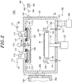
- Fig. 2 is a cross-sectional view showing a schematic configuration of an example of the process module PM1.
- the process modules PM2 to PM8 may have the same configuration as that of the process module PM1.
- the process module PM1 includes a processing chamber 101 made of a metal such as aluminum or stainless steel.
- the processing chamber 101 is grounded.
- the cathode unit 110 includes a target electrode 111, a target 112, a power supply 113, and a cathode magnet 114.
- the target electrode 111 functions as a cathode electrode and is attached to the ceiling portion of the processing chamber 101 via an insulating member 116.
- the target electrode 111 holds the target 112.
- the target 112 is made of a material forming a film to be deposited, and is made of a magnetic material, a non-magnetic material, or an insulating material.
- the targets 112 may be made of the same material or may be made of different materials.
- the power supply 113 is, e.g., a DC power supply, and applies a negative DC voltage to the target electrode 111.
- the power supply 113 may be an AC power supply.
- the cathode magnet 114 is disposed on an upper surface of the target electrode 111, and a magnet driving part 115 is connected to the cathode magnet 114.
- a shutter 120 is disposed directly under the multiple cathode units 110.
- the shutter 120 has a disc shape having a size that covers a projection area of the targets 112, and is rotatable about a rotation shaft 122 disposed at the center of the ceiling portion.
- the rotation shaft 122 is connected to a rotation mechanism 123 disposed above the processing chamber, and the shutter 120 is rotated by the rotation mechanism 123.
- the shutter 120 has an opening 121 that is slightly greater than the target 112.
- the opening 121 corresponds to the target 112 to be used, and the other targets 112 are shielded by the shutter 120.
- a substrate holder 130 for horizontally holding the substrate W is disposed in a lower region of the processing chamber 101 to face the cathode units 110.
- the substrate holder 130 is provided with a substantially disc-shaped electrostatic chuck (not shown) for attracting and holding the substrate W and a temperature controller (not shown) for controlling a temperature of the substrate W.
- the substrate holder 130 is provided with three elevating pins (not shown) that can protrude and retract with respect to the upper surface of the substrate holder 130, so that the substrate W can be transferred to the substrate holder 130.
- a support shaft 131 extends downward from the center of a bottom surface of the substrate holder 130 to penetrate through the processing chamber 101, and is connected to a driving mechanism 132 under the processing chamber 101.
- the driving mechanism 132 is configured to rotate and vertically move the substrate holder 130 via the support shaft 131.
- a space between the support shaft 131 and a bottom wall of the processing chamber 101 is sealed by a magnetic fluid seal or the like.
- a ring magnet 140 for applying a magnetic field to the substrate W is disposed around the substrate holder 130.
- the ring magnet 140 is configured to apply a magnetic field to the notch of the substrate W at an arbitrary angle.
- a magnet support 135 is disposed around the substrate holder 130.
- An inwardly protruding protrusion 136 is formed at a lower end of an inner circumference of the ring magnet 140.
- the ring magnet 140 can be supported by a support shaft 41, and can be vertically moved by the support shaft 141.
- the ring magnet 140 can be placed on the substrate holder 130 by aligning the positions of the magnet support 135 and the protrusion 136 by rotating the substrate holder 130. In the case of forming a magnetic film, as shown in Fig.
- the support shaft 141 is lowered to separate the ring magnet 140 and the support shaft 141.
- the ring magnet 140 is located at a height position corresponding to the substrate W held by the substrate holder 130.
- the direction of the magnetic field of the ring magnet 140 at this time is adjusted in advance to form a specific angle with respect to the notch of the substrate W. Since the ring magnet 140 is placed on the substrate holder 130, the ring magnet 140 rotates together with the substrate holder 130.
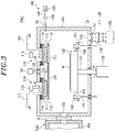
- a non-magnetic film as shown in Fig.
- the ring magnet 140 is separated from the substrate holder 130 by misaligning the positions of the magnet support 135 and the protrusion 136. Then, the ring magnet 140 is supported by the support shaft 141, and the ring magnet 140 is lowered with respect to the substrate supporter 130 to prevent the magnetic field from being applied to the substrate W. Accordingly, it is possible to prevent the magnetic field from adversely affecting the film formation of the non-magnetic film.
- the substrate holder 130 is also raised from the ring magnet 140 when the substrate W is loaded and unloaded.
- An exhaust 150 is disposed at the bottom portion of the processing chamber 101.
- the exhaust 150 includes an exhaust line 151 connected to an exhaust port 102 formed at the bottom portion of the processing chamber 101, a pressure control valve 152, and a vacuum pump 153.
- the vacuum pump 153 exhausts the inside of the processing chamber 101 through the exhaust line 151.
- the pressure control valve 152 is disposed in the exhaust line 151 to control a pressure in the processing chamber 101.
- a loading/unloading port 103 for loading/unloading the substrate W is disposed on the sidewall of the processing chamber.
- the loading/unloading port 103 is opened and closed by the above-described gate valve G.
- a gas supplier 160 is disposed at an upper portion of the sidewall of the processing chamber 101.
- the gas supplier 160 includes a gas inlet nozzle 161, a gas supply line 162, and a gas supply source 163.
- a noble gas e.g., Ar, Ne, Kr, or the like (Ar in the example of Fig. 2 )
- Ar e.g., Ar, Ne, Kr, or the like
- a gas control device group 164 e.g., a valve, a flow rate controller such as a mass flow controller, or the like is disposed in the gas supply line 162.
- Fig. 4 is a cross-sectional view showing a schematic configuration of the transfer module TM1.
- the transfer modules TM2 to TM4 basically have the same configuration as that of the transfer module TM1.
- the transfer module TM1 includes the container 30a, the transfer mechanism 31a, the aligner 32a, and an exhaust mechanism 61.
- the exhaust mechanism 61 exhausts the inside of the container 30a to set a pressure in the container 30a to a predetermined vacuum level.
- the transfer mechanism 31a has a driving mechanism 51, a base portion 52, a rotatable and extensible/contractible portion 53, and a substrate support arm 54.
- the driving mechanism 51 is disposed below the container 30a and configured to rotate a driving shaft 51a.
- the base portion 52 is fixed to the center of the bottom portion in the container 30a, and the driving shaft 51a is inserted into the base portion 52.
- the rotatable and extensible/contractible portion 53 has an articulated structure that is rotatable and extensible/contractible by the driving mechanism 51.
- the substrate support arm 54 supports and delivers the substrate W. As shown in Fig. 5 , the substrate support arm 54 has a U shape and, thus, the substrate W can be delivered to a destination while avoiding the substrate support pins 81.
- the transfer mechanism 31a does not necessarily have the illustrated articulated type, and may have another type such as a frog leg type, a linear type, or the like.
- the aligner 32a has a driving mechanism 71, a driving shaft 72, a substrate support portion 73, and an optical sensor 74.
- the aligner 32a is disposed near the loading port of the process module to which the substrate W is transferred by the transfer mechanism 31a.
- the aligner 32a is disposed near the loading port of the process module PM1.
- the driving mechanism 71 is disposed below the container 30a and has the driving shaft 72 extending vertically upward into the container 30a.
- the driving mechanism 71 is configured to rotate and vertically move the drive shaft 72.
- the substrate support portion 73 is disposed at an upper end of the driving shaft 72, and is provided with three substrate support pins (only two are shown) 73a for supporting the substrate W.
- the optical sensor 74 has a light emitting part 74a and a light receiving part 74b, and detects the notch position of the substrate W when the light from the light emitting part 74a is received by the light receiving part 74b.
- the substrate W is rotated while being supported by the substrate support portion 73, light L emitted from the light emitting part 74a is received by the light receiving part 74b when the notch 82 of the substrate W reaches a position corresponding to the light L as shown in Fig. 6 . Accordingly, the notch position of the substrate W is detected.
- a detection signal obtained when the light is received by the light receiving part 74b is transmitted to the controller 4, and the alignment of the substrate W is performed based on the detection signal. Further, the eccentricity of the substrate W from the position where the light L passes through the notch 82 can be corrected.
- a vacuum bellows 75 is disposed between the bottom surface of the bottom wall of the container 30a and the driving mechanism 71.
- the substrate W can be transferred from the transfer mechanism 31a to the aligner 32a as shown in Figs. 7A and 7B .
- the substrate W supported by the support arm 54 is transferred to a position directly above the substrate support portion 73.
- the driving mechanism 71 raises the substrate support portion 73 via the driving shaft 72 so that the substrate W can be received on the substrate support pins 73a.
- the transfer of the substrate W from the aligner 32a to the transfer mechanism 31a may be realized by performing the operations illustrated in Figs. 7A and 7B in the reverse order.
- the aligner 32a is disposed at a position where the operation of receiving the substrate W from the transfer mechanism 31a and transferring the aligned substrate W to the process module PM1 can be effectively performed. From the above, it is preferable that the aligner 32a is disposed near the loading port of the process module PM1 (see Fig. 1 ). Further, as shown in Fig. 8 , it is preferable that the aligner 32a is disposed on a transfer path on which the transfer mechanism 31a of the transfer module TM1 accesses the substrate holder of the process module PM1 connected to the transfer module TM1. Specifically, in the example of Fig.
- the aligner 32a is disposed on a line that connects the rotation center of the transfer mechanism 31a (the portion of the driving shaft 51a corresponding to the center of the base portion 52) and the center of the substrate holder 130 of the process module PM1. Accordingly, it is possible to minimize a transfer route in which the substrate W is transferred to the aligner and then loaded into the process module PM1 and transferred to the substrate holder 130 by the transfer mechanism 31a. This is also applied to the aligners 32b, 32c and 32d. In the example of Fig. 8 , the aligner 32a is disposed near the loading port of the process module PM1.
- the substrate W is taken out from the FOUP 20 on the load port 22 and transferred to the load-lock module LLM1 by the transfer device 24.
- the load-lock module LLM1 is maintained in an atmospheric pressure state, and is evacuated after the substrate W is received.
- the substrate W is unloaded from the load-lock module LLM1 by the transfer mechanism 31a of the transfer module TM1 in the transfer part 12.
- the unloaded substrate W is transferred to the aligner 32a by the transfer mechanism 31a and aligned by the aligner 32a.
- the aligned substrate W is transferred to the process module PM1 by the transfer mechanism 31a.
- the gate valve G is opened, and the substrate W supported by the substrate support arm 54 of the transfer mechanism 31a is loaded into the processing chamber 101 through the loading/unloading port 103 and held on the substrate holder 130.
- the substrate holder 130 is located at the position shown in Fig. 3 .
- the gate valve G is closed, and the inside of the processing chamber 101 is evacuated by the vacuum pump 153 of the exhaust 150.
- the gas supplier 160 introduces an inert gas, e.g., Ar gas, and controls a pressure in the processing chamber 101 to a desired vacuum level. If necessary, a temperature of the substrate W is adjusted to a predetermined temperature by the temperature controller of the substrate holder 130.
- a desired target 112 is selected from the plurality of targets 112 and subjected to sputtering film formation.
- other targets except the selected target are shielded by the shutter 120.
- a power is supplied to the selected target 112 from the corresponding power supply 113 through the corresponding target electrode 112 while rotating the substrate holder 130 by the driving mechanism 132.
- the cathode magnets 114 are driven by the magnet driving parts 115.
- high-density plasma is generated from the inert gas (Ar gas) by the electric field generated by the voltage applied to the target 112 and the magnetic field generated by the cathode magnets 114.
- the target 112 is sputtered by the plasma thus generated, and sputtered particles are released. These sputtered particles are deposited on the substrate W to form a desired film.
- the direction of the magnetic field of the ring magnet 140 is adjusted in advance to form a specific angle corresponding to the magnetic film to be formed with respect to the notch of the substrate W. Then, the ring magnet 140 is placed on the substrate holder 130 by aligning the positions of the magnet support 135 and the protrusion 136, and the substrate holder 130 is located at the height position shown in Fig. 2 . Then, the sputtering film formation is performed while rotating the ring magnet 140 together with the substrate holder 130.
- the substrate holder 130 and the ring magnet 140 are located at the height positions illustrated in Fig. 3 , and the sputtering film formation is performed in a state where the magnetic field of the ring magnet 140 does not affect the substrate W.
- the ring magnet 140 is not placed on the substrate holder 130, and only the substrate holder 130 is rotated.
- a plurality of films can be formed to correspond to a plurality of targets 112. Further, a single film may be formed using the plurality of targets 112 made of the same material. In other words, in the process module PM1, one or multiple predetermined films are formed on the substrate W by sputtering.
- the gate valve G on the unloading side of the process module PM1 is opened, and the substrate W is unloaded by the transfer mechanism 31b of the transfer module TM2.
- the unloaded substrate W is transferred to the aligner 32b by the transfer mechanism 31b and aligned by the aligner 32b, and then transferred to the process module PM3 by the transfer mechanism 31b.
- the process module PM3 similarly to the process module PM1, one or multiple predetermined films are formed on the substrate W by sputtering.
- the gate valve G on the unloading side of the process module PM3 is opened, and the substrate W is unloaded by the transfer mechanism 31c of the transfer module TM3.
- the unloaded substrate W is transferred to the aligner 32c by the transfer mechanism 31c and aligned by the aligner 32c, and then transferred to the process module PM5 by the transfer mechanism 31c.
- the process module PM5 for example, similarly to the process module PM1, one or multiple predetermined films are formed on the substrate W by sputtering.
- the gate valve G on the unloading side of the process module PM5 is opened, and the substrate W is unloaded by the transfer mechanism 31d of the transfer module TM4.
- the unloaded substrate W is transferred to the aligner 32d by the transfer mechanism 31d and aligned by the aligner 32d, and then transferred to the process module PM7 by the transfer mechanism 31d.
- the process module PM7 for example, similarly to the process module PM1, one or multiple predetermined films are formed on the substrate W by sputtering.
- the gate valve G on the unloading side of the process module PM7 is opened, and the substrate W is unloaded by the transfer mechanism 31d of the transfer module TM4.
- the unloaded substrate W is transferred to the aligner 32d by the transfer mechanism 31d and aligned (by the aligner 32d), and then transferred to the process module PM8 by the transfer mechanism 31d.
- the process module PM8 for example, similarly to the process module PM1, one or multiple predetermined films are formed on the substrate W by sputtering.
- the substrates W are sequentially transferred to the process modules PM6, PM4, and PM2 by the transfer mechanisms 31c, 31b, and 31a of the transfer modules TM3, TM2, and TM1 through the aligners 32c, 32b, and 32a, respectively, and subjected to the same sputtering film formation as that performed in the process module PM1.
- the substrate W is transferred to the load-lock module LLM2 by the transfer mechanism 31a.
- the load-lock module LLM2 is in a vacuum state, and opened to the atmosphere after the wafer W is received. Then, the substrate W in the load-lock module LLM2 is transferred into the FOUP 20 of the load port 22 by the transfer device 24.
- the substrates W can be sequentially and serially transferred to the plurality of process modules in a U-shape and subjected to a series of film forming processes.
- the delivery parts 41, 42, and 43 function as transfer buffers where the substrates W temporarily stand by when the access of the transfer mechanisms 31a to 31d is delayed.
- the plurality of targets 112 of some process modules may be non-magnetic. In that case, the ring magnet 140 is unnecessary. Further, it is not necessary that all the process modules PM1 to PM8 are film forming apparatuses for performing sputtering film formation.
- the process module PM1 may be used as a pre-cleaning apparatus. Further, when it is necessary to form an oxide film, some of the process modules may be used as film forming apparatuses having therein an oxidation mechanism, or some other process modules may be dedicated to oxidation treatment.
- a direction M of the magnetic field generated by the ring magnet 140 and an angle ⁇ of the position of the notch 82 of the substrate W are different depending on materials, so that it is necessary to adjust the angle ⁇ to a specific angle depending on the material of the magnetic film. Therefore, it is necessary to align the substrate W at the time of transferring the substrate to the process module. Further, even when it is not necessary to adjust the angle of the substrate W, it may be necessary to correct the position of the substrate W to improve the stability of the transfer accuracy of the substrate W.
- the aligner is disposed in the atmospheric transfer chamber, so that the transfer of the substrate becomes extremely complicated in the case aligning the substrate whenever the substrate is transferred to the plurality of process modules. Further, although it may be considered that the delivery part between the transfer modules serves as the aligner, the transfer of the substrate becomes complicated in this case as well. Therefore, it is difficult to maintain a high productivity in both cases.
- the aligners 32a, 32b, 32c, and 32d are respectively disposed in the plurality of transfer modules TM1 to TM4 having the transfer mechanisms, and the alignment of the substrate W transferred to the process module connected to each transfer module was performed by the aligner of the corresponding transfer module. Accordingly, even when the substrate W is aligned whenever the substrate W is transferred to each process module, it is not necessary to transfer the substrate W to the outside of the corresponding transfer module in order to perform the alignment, which makes it possible to maintain a high productivity.
- the aligners 32a, 32b, 32c, and 32d are disposed near the loading port of the process module to which the substrate W will be transferred (see Fig. 1 ). Accordingly, the aligned substrate W can be efficiently transferred to the corresponding process module. Further, it is preferable that the aligners 32a, 32b, 32c and 32d are disposed on the path where the substrate W is transferred to the corresponding process modules by the corresponding transfer mechanisms 31a, 31b, 31c and 31d (see
- the transfer mechanisms 31a, 31b, 31c, and 31d deliver the substrates W to the aligners 32a, 32b, 32c, and 32d and transfer the aligned substrates W to the process modules PM1, PM3, PM5, and PM7.
- the productivity can be further improved.
- the aligner 32a is disposed on a line that connects the rotation center of the transfer mechanism 31a and the center of the substrate holder 130 of the process module PM1 that is the transfer destination.
- Fig. 10 is a plan view schematically showing a substrate processing system according to the second embodiment.
- the substrate processing system 1' of the present embodiment basically has the same configuration as that of the substrate processing system 1 of the first embodiment, and includes four transfer modules TM1 to TM4 and eight process modules PM1 to PM8.
- each of the transfer modules TM1, TM2, TM3, and TM4 has transfer mechanism 31a', 31b', 31c', and 31d', each having two substrate support arms 54a and 54b, instead of the transfer mechanisms 31a, 31b, 31c, and 31d of the first embodiment.
- the substrates W can be transferred simultaneously by the two substrate support arms 54a and 54b, so that the productivity can be further improved.
- the two substrate support arms 54a and 54b can simultaneously load or unload the substrates into or from two process modules.
- the substrate W can be transferred to the process module PM3 by the substrate support arm 54a of the transfer mechanism 31b' and, at the same time, the substrate W can be transferred to the process module PM2 by the substrate support arm 54b.
- the transfer modules TM1, TM2, TM3, and TM4 have aligners 32a', 32b', 32c', and 32d' in addition to the aligners 32a, 32b, 32c, and 32d that are the same as those of the first embodiment.
- the aligners 32a, 32b, 32c, and 32d are used to align the substrates W at the time of loading the substrates W into the process modules PM1, PM3, PM5, and PM7 by the substrate support arms 54a of the transfer mechanisms 31a', 31b', 31c', and 31d', respectively.
- the aligners 32a', 32b', 32c', and 32d' are used to align the substrates W at the time of loading the substrates W into the process modules PM6, PM4, and PM2, and the load-lock module LLM2 by the substrate support arms 54b of the transfer mechanisms 31a', 31b', 31c', and 31d', respectively.
- the aligners 32a', 32b', 32c', and 32d' are disposed near the loading ports of the process modules to which the substrates W will be transferred and disposed on the path where the substrates W are transferred to the corresponding transfer modules by the corresponding transfer mechanisms 31a', 31b', 31c', and 31d'. Accordingly, it is possible to effectively perform the operation in which the transfer mechanisms 31a', 31b', 31c', and 31d' deliver the substrates W to the aligners 32a', 32b', 32c', and 32d', and transfer the aligned substrates W to the process modules PM6, PM4, and PM2 and the load-lock module LLM2. Hence, the productivity can be further improved.
- the aligners 32a', 32b', 32c', and 32d' are disposed on the line that connects the rotation centers of the transfer mechanisms 31a', 31b', 31c', and 31d' and the center of the substrate holder that is the transfer destination. Accordingly, it is possible to minimize the transfer route where the substrates W are transferred to the aligners 32a', 32b', 32c', and 32d', and then loaded into the load-lock module LLM2 and the process module PM2, PM4, and PM6 and transferred to the substrate holders by the transfer mechanism 31a', 31b', 31c', and 31d'.
- the processing system 1 of the embodiment is merely an example and may be modified as long as a plurality of substrates is serially transferred to a plurality of process modules connected to a plurality of transfer modules and processed. Further, in the above embodiment, a plurality of substrates are serially transferred in a U shape.
- the present disclosure is not limited thereto.
- the case of manufacturing the head of the hard disk drive has been described as an example. However, the present disclosure is not limited thereto, and may also be applied to the case of manufacturing a multilayer film including another magnetic film.
- the processing is not limited to sputtering film formation.
Landscapes
- Chemical & Material Sciences (AREA)
- Engineering & Computer Science (AREA)
- Physics & Mathematics (AREA)
- Plasma & Fusion (AREA)
- Analytical Chemistry (AREA)
- Materials Engineering (AREA)
- Chemical Kinetics & Catalysis (AREA)
- Mechanical Engineering (AREA)
- Metallurgy (AREA)
- Organic Chemistry (AREA)
- Container, Conveyance, Adherence, Positioning, Of Wafer (AREA)
- Physical Vapour Deposition (AREA)
- Robotics (AREA)
Abstract
Description
- The present disclosure relates to a substrate processing system and a substrate processing method.
- As a processing apparatus for performing a plurality of processes on a substrate, there is known a processing apparatus including a transfer part in which multiple transfer modules, each having a substrate transfer device, are arranged in one row and a plurality of process modules arranged on both sides of transfer chambers and configured to transfer substrates sequentially and serially in a U shape and perform a series of processes (see, e.g., Patent Document 1).
- In addition, there is suggested a technique for detecting a direction of a notch of a substrate (object to be processed) using an aligner disposed in an atmospheric transfer chamber and performing pre-alignment of the substrate before substrates are sequentially and serially transferred to multiple process modules and processed (see, e.g., Patent Document 2).
-
- Patent Document 1:
Japanese Patent Publication No. 6160614 - Patent Document 2:
Japanese Laid-open Patent Publication No. 2017-103415 - The present disclosure provides a substrate processing system and a substrate processing method capable of maintaining a high productivity even when a substrate is aligned whenever the substrate is transferred to each of a plurality of process modules connected to a plurality of transfer modules in the case of serially transferring a plurality of substrates to the process modules and processing them.
- In accordance with an aspect of the present disclosure, there is provided a substrate processing system including a plurality of transfer modules having transfer mechanisms for transferring substrates, and a plurality of process modules connected to the plurality of transfer modules. The transfer mechanisms of the plurality of transfer modules transfer a plurality of substrates sequentially and serially to the plurality of process modules. Each of the plurality of transfer modules has an aligner for aligning a substrate when transferring the same to the process module connected to the relevant transfer module.
- In accordance with the present disclosure, there are provided a substrate processing system and a substrate processing method capable of maintaining a high productivity even when a substrate is aligned whenever the substrate is transferred to each of a plurality of process modules connected to a plurality of transfer modules in the case of serially transferring a plurality of substrates to the process modules and processing them.
-
-
Fig. 1 is a plan view schematically showing a substrate processing system according to a first embodiment. -
Fig. 2 is a cross-sectional view showing a schematic configuration of an example of a process module attached to the substrate processing system ofFig. 1 . -
Fig. 3 is a cross-sectional view showing a position of a substrate holder at the time of forming a non-magnetic film in the process module ofFig. 2 . -
Fig. 4 is a cross-sectional view showing a schematic configuration of a transfer module attached to the substrate processing system ofFig. 1 . -
Fig. 5 is a plan view showing a substrate support arm of a transfer mechanism disposed in the transfer module. -
Fig. 6 explains a notch position detection method using an optical sensor in an aligner. -
Fig. 7A explains transfer of a substrate from the transfer mechanism in the transfer module to the aligner. -
Fig. 7B explains transfer of a substrate from the transfer mechanism in the transfer module to the aligner. -
Fig. 8 shows a desired arrangement position of the aligner in the transfer module. -
Fig. 9 explains a relationship between a direction of a magnetic field of a ring magnet and a notch position of a substrate in the case of forming a magnetic film in the process module. -
Fig. 10 a plan view schematically showing a substrate processing system according to a second embodiment. - Hereinafter, embodiments will be described with reference to the accompanying drawings.
- First, a first embodiment will be described.
-
Fig. 1 is a plan view schematically showing a substrate processing system according to the first embodiment. - The substrate processing system 1 performs a plurality of processes on a substrate, and includes a
processing part 2, a loading/unloadingpart 3 for holding a plurality of substrates and loading/unloading a substrate to/from theprocessing part 2, and acontroller 4. The substrate is not particularly limited, but is a semiconductor wafer (hereinafter, simply referred to as "wafer"), for example. - The
processing part 2 includes a plurality of (eight in this example) process modules PM1 to PM8 for performing predetermined vacuum processing on substrates W, and atransfer part 12 having a plurality of transfer modules TM1 to TM4 for sequentially transferring substrates W to the process modules PM1 to PM8. - The transfer modules TM1, TM2, TM3, and TM4 have
containers transfer mechanisms Delivery parts containers - In the
transfer part 12, the transfer modules TM1 to TM4 are arranged in one row in the Y direction in the drawing, and four of the process modules PM1 to PM8 are connected to each of two sides of thetransfer part 12 through gate valves G that can be opened and closed. The gate valves G of the process modules PM1 to PM8 are opened when the transfer mechanism of the transfer module accesses the process modules, and are closed during processing. - The loading/unloading
part 3 is connected to one end of theprocessing part 2. The loading/unloadingpart 3 includes an atmospheric transfer chamber (EFEM) 21, threeload ports 22 connected to theatmospheric transfer chamber 21, two load-lock modules LLM1 and LLM2, and atransfer device 24 disposed in theatmospheric transfer chamber 21. - The
atmosphere transfer chamber 21 has a rectangular parallelepiped shape with the X direction as a longitudinal direction in the drawing. The threeload ports 22 are disposed at a long sidewall of theatmospheric transfer chamber 21 opposite to a sidewall facing theprocessing part 2. Eachload port 22 has a placement table 25 and atransfer port 26. A front opening unified pod (FOUP) 20 that is a wafer storage container accommodating a plurality of wafers is placed on the placement table 25, and the FOUP 20 on the placement table 25 is connected in a sealed state to theatmospheric transfer chamber 21 through thetransfer port 26. - The two load-lock modules LLM1 and LLM2 allow wafers W to be transferred between the
atmospheric transfer chamber 21 maintained at an atmospheric pressure and thetransfer part 12 maintained at a vacuum atmosphere, and a pressure in each of the load-lock modules LLM1 and LLM2 is variable between an atmospheric pressure and a vacuum level similar to that in thetransfer part 12. Each of the two load-lock modules LLM1 and LLM2 has two transfer ports. One of the two transfer ports is connected to the long sidewall of theatmospheric transfer chamber 21 facing theprocessing part 2 through a gate valve G2. The other transfer port is connected to thetransfer part 12 of theprocessing part 2 through the gate valve G1. - The load-lock module LLM1 is used when the wafer W is transferred from the loading/unloading
part 3 to theprocessing part 2, and the load-lock module LLM2 is used when the wafer W is transferred from theprocessing part 2 to the loading/unloadingpart 3. Further, processing such as degassing or the like may be performed in the load-lock modules LLM1 and LLM2. - The
transfer device 24 in theatmospheric transfer chamber 21 has, e.g., an articulated structure, and transfers wafers W to theFOUP 20 on theload port 22 and the load-lock modules LLM1 and LLM2. Specifically, thetransfer device 24 takes out an unprocessed wafer W from theFOUP 20 of theload port 22 and transfers the wafer W to the load-lock module LLM1. Further, thetransfer device 24 receives a processed wafer W transferred from theprocessing part 2 to the load-lock module LLM2 and transfers the wafer W to theFOUP 20 of theload port 22. - In the
processing part 2, the process modules PM1, PM3, PM5, and PM7 are arranged on one side of thetransfer part 12 in that order from the load-lock module LLM1 side, and the process modules PM2, PM4, PM6, and PM8 are arranged on another side of thetransfer part 12 in that order from the load-lock module LLM2 side. Further, in thetransfer part 12, the transfer modules TM1, TM2, TM3, and TM4 are arranged in that order from the load-lock modules LLM1 and LLM2 side. - Further,
aligners containers aligners transfer mechanisms - The
transfer mechanism 31a of the transfer module TM1 is accessible to the load-lock modules LLM1 and LLM2, the process modules PM1 and PM2, thedelivery part 41, and thealigner 32a. Thetransfer mechanism 31b of the transfer module TM2 is accessible to the process modules PM1, PM2, PM3, and PM4, thedelivery parts aligner 32b. Thetransfer mechanism 31c of the transfer module TM3 is accessible to the process modules PM3, PM4, PM5, and PM6, thedelivery parts aligner 32c. Thetransfer mechanism 31d of the transfer module TM4 is accessible to the process modules PM5, PM6, PM7, and PM8, thedelivery part 43, and thealigner 32d. - Since the
transfer device 24 and the transfer modules TM1 to TM4 of thetransfer part 12 are configured as described above, the substrates W taken out from theFOUP 20 are serially transferred in one direction along a substantially U-shaped path in the order of the process modules PM1, PM3, PM5, PM7, PM8, PM6, PM4, and PM2, processed in the respective process modules in theprocessing part 2, and returned to theFOUP 20. - The
controller 4 controls individual components of the substrate processing system 1, such as the transfer modules TM1 to TM4 (transfermechanisms 31a to 31d), thetransfer device 24, the process modules PM1 to PM8, the load-lock modules LLM1 and LLM2, thetransfer part 12, the gate valves G, G1, and G2, and the like. Thecontroller 4 is a computer, and includes a main controller having a CPU, an input device, an output device, a display device, and a storage device. The storage device is provided with a storage medium in which processing recipes are stored. The main controller causes the substrate processing system 1 to execute a predetermined operation based on the processing recipe retrieved from the storage medium. - The substrate processing system 1 may be desirably used for manufacturing a multilayer film including a plurality of magnetic films. A hard disk drive (HDD) head may be an example of a product that requires such a multilayer film. In the case of forming a plurality of magnetic films, it may be necessary to control a notch angle of the substrate W and a magnetization direction for each magnetic film.
- Next, the process module will be described.
-
Fig. 2 is a cross-sectional view showing a schematic configuration of an example of the process module PM1. The process modules PM2 to PM8 may have the same configuration as that of the process module PM1. - As shown in
Fig. 2 , the process module PM1 includes aprocessing chamber 101 made of a metal such as aluminum or stainless steel. Theprocessing chamber 101 is grounded. - At a ceiling portion of the
processing chamber 101,multiple cathode units 110 are arranged concentrically with respect to the center of the ceiling portion. The number of thecathode units 110 is not particularly limited as long as it is plural. For example, fourcathode units 110 may be provided. Thecathode unit 110 includes atarget electrode 111, atarget 112, apower supply 113, and acathode magnet 114. - The
target electrode 111 functions as a cathode electrode and is attached to the ceiling portion of theprocessing chamber 101 via an insulatingmember 116. Thetarget electrode 111 holds thetarget 112. Thetarget 112 is made of a material forming a film to be deposited, and is made of a magnetic material, a non-magnetic material, or an insulating material. Thetargets 112 may be made of the same material or may be made of different materials. Thepower supply 113 is, e.g., a DC power supply, and applies a negative DC voltage to thetarget electrode 111. Thepower supply 113 may be an AC power supply. - The
cathode magnet 114 is disposed on an upper surface of thetarget electrode 111, and amagnet driving part 115 is connected to thecathode magnet 114. - A
shutter 120 is disposed directly under themultiple cathode units 110. Theshutter 120 has a disc shape having a size that covers a projection area of thetargets 112, and is rotatable about arotation shaft 122 disposed at the center of the ceiling portion. Therotation shaft 122 is connected to arotation mechanism 123 disposed above the processing chamber, and theshutter 120 is rotated by therotation mechanism 123. Theshutter 120 has anopening 121 that is slightly greater than thetarget 112. Theopening 121 corresponds to thetarget 112 to be used, and theother targets 112 are shielded by theshutter 120. - A
substrate holder 130 for horizontally holding the substrate W is disposed in a lower region of theprocessing chamber 101 to face thecathode units 110. Thesubstrate holder 130 is provided with a substantially disc-shaped electrostatic chuck (not shown) for attracting and holding the substrate W and a temperature controller (not shown) for controlling a temperature of the substrate W. Further, thesubstrate holder 130 is provided with three elevating pins (not shown) that can protrude and retract with respect to the upper surface of thesubstrate holder 130, so that the substrate W can be transferred to thesubstrate holder 130. - A
support shaft 131 extends downward from the center of a bottom surface of thesubstrate holder 130 to penetrate through theprocessing chamber 101, and is connected to adriving mechanism 132 under theprocessing chamber 101. Thedriving mechanism 132 is configured to rotate and vertically move thesubstrate holder 130 via thesupport shaft 131. A space between thesupport shaft 131 and a bottom wall of theprocessing chamber 101 is sealed by a magnetic fluid seal or the like. - A
ring magnet 140 for applying a magnetic field to the substrate W is disposed around thesubstrate holder 130. Thering magnet 140 is configured to apply a magnetic field to the notch of the substrate W at an arbitrary angle. Amagnet support 135 is disposed around thesubstrate holder 130. An inwardly protrudingprotrusion 136 is formed at a lower end of an inner circumference of thering magnet 140. Further, thering magnet 140 can be supported by asupport shaft 41, and can be vertically moved by thesupport shaft 141. Thering magnet 140 can be placed on thesubstrate holder 130 by aligning the positions of themagnet support 135 and theprotrusion 136 by rotating thesubstrate holder 130. In the case of forming a magnetic film, as shown inFig. 2 , in a state where thering magnet 140 is placed on thesubstrate holder 130, thesupport shaft 141 is lowered to separate thering magnet 140 and thesupport shaft 141. In that case, thering magnet 140 is located at a height position corresponding to the substrate W held by thesubstrate holder 130. The direction of the magnetic field of thering magnet 140 at this time is adjusted in advance to form a specific angle with respect to the notch of the substrate W. Since thering magnet 140 is placed on thesubstrate holder 130, thering magnet 140 rotates together with thesubstrate holder 130. In the case of forming a non-magnetic film, as shown inFig. 3 , thering magnet 140 is separated from thesubstrate holder 130 by misaligning the positions of themagnet support 135 and theprotrusion 136. Then, thering magnet 140 is supported by thesupport shaft 141, and thering magnet 140 is lowered with respect to thesubstrate supporter 130 to prevent the magnetic field from being applied to the substrate W. Accordingly, it is possible to prevent the magnetic field from adversely affecting the film formation of the non-magnetic film. Thesubstrate holder 130 is also raised from thering magnet 140 when the substrate W is loaded and unloaded. - An
exhaust 150 is disposed at the bottom portion of theprocessing chamber 101. Theexhaust 150 includes anexhaust line 151 connected to anexhaust port 102 formed at the bottom portion of theprocessing chamber 101, apressure control valve 152, and avacuum pump 153. Thevacuum pump 153 exhausts the inside of theprocessing chamber 101 through theexhaust line 151. Further, thepressure control valve 152 is disposed in theexhaust line 151 to control a pressure in theprocessing chamber 101. - A loading/unloading
port 103 for loading/unloading the substrate W is disposed on the sidewall of the processing chamber. The loading/unloadingport 103 is opened and closed by the above-described gate valve G. - A
gas supplier 160 is disposed at an upper portion of the sidewall of theprocessing chamber 101. Thegas supplier 160 includes agas inlet nozzle 161, agas supply line 162, and agas supply source 163. A noble gas, e.g., Ar, Ne, Kr, or the like (Ar in the example ofFig. 2 ), is supplied as a plasma generation gas from thegas supply source 163 into theprocessing chamber 101 through thegas supply line 162 and thegas inlet nozzle 161. A gascontrol device group 164, e.g., a valve, a flow rate controller such as a mass flow controller, or the like is disposed in thegas supply line 162. - Next, the transfer module will be described.
-
Fig. 4 is a cross-sectional view showing a schematic configuration of the transfer module TM1. The transfer modules TM2 to TM4 basically have the same configuration as that of the transfer module TM1. - As shown in
Fig. 4 , the transfer module TM1 includes thecontainer 30a, thetransfer mechanism 31a, thealigner 32a, and anexhaust mechanism 61. - The
exhaust mechanism 61 exhausts the inside of thecontainer 30a to set a pressure in thecontainer 30a to a predetermined vacuum level. - The
transfer mechanism 31a has adriving mechanism 51, abase portion 52, a rotatable and extensible/contractible portion 53, and asubstrate support arm 54. - The
driving mechanism 51 is disposed below thecontainer 30a and configured to rotate a drivingshaft 51a. Thebase portion 52 is fixed to the center of the bottom portion in thecontainer 30a, and the drivingshaft 51a is inserted into thebase portion 52. - The rotatable and extensible/
contractible portion 53 has an articulated structure that is rotatable and extensible/contractible by thedriving mechanism 51. Thesubstrate support arm 54 supports and delivers the substrate W. As shown inFig. 5 , thesubstrate support arm 54 has a U shape and, thus, the substrate W can be delivered to a destination while avoiding the substrate support pins 81. Further, thetransfer mechanism 31a does not necessarily have the illustrated articulated type, and may have another type such as a frog leg type, a linear type, or the like. - The
aligner 32a has adriving mechanism 71, a drivingshaft 72, asubstrate support portion 73, and anoptical sensor 74. In thecontainer 30a, thealigner 32a is disposed near the loading port of the process module to which the substrate W is transferred by thetransfer mechanism 31a. In this example, thealigner 32a is disposed near the loading port of the process module PM1. - The
driving mechanism 71 is disposed below thecontainer 30a and has the drivingshaft 72 extending vertically upward into thecontainer 30a. Thedriving mechanism 71 is configured to rotate and vertically move thedrive shaft 72. Thesubstrate support portion 73 is disposed at an upper end of the drivingshaft 72, and is provided with three substrate support pins (only two are shown) 73a for supporting the substrate W. - The
optical sensor 74 has alight emitting part 74a and alight receiving part 74b, and detects the notch position of the substrate W when the light from thelight emitting part 74a is received by thelight receiving part 74b. In other words, when the substrate W is rotated while being supported by thesubstrate support portion 73, light L emitted from thelight emitting part 74a is received by thelight receiving part 74b when thenotch 82 of the substrate W reaches a position corresponding to the light L as shown inFig. 6 . Accordingly, the notch position of the substrate W is detected. A detection signal obtained when the light is received by thelight receiving part 74b is transmitted to thecontroller 4, and the alignment of the substrate W is performed based on the detection signal. Further, the eccentricity of the substrate W from the position where the light L passes through thenotch 82 can be corrected. In addition, a vacuum bellows 75 is disposed between the bottom surface of the bottom wall of thecontainer 30a and thedriving mechanism 71. - The substrate W can be transferred from the
transfer mechanism 31a to thealigner 32a as shown inFigs. 7A and 7B . In other words, first, as shown inFig. 7A , in a state where height positions of the substrate support pins 73a of thesubstrate support portion 73 are lower than the height position of the substrate W supported by thesubstrate support arm 54, the substrate W supported by thesupport arm 54 is transferred to a position directly above thesubstrate support portion 73. Next, as shown inFig. 7B , thedriving mechanism 71 raises thesubstrate support portion 73 via the drivingshaft 72 so that the substrate W can be received on thesubstrate support pins 73a. The transfer of the substrate W from thealigner 32a to thetransfer mechanism 31a may be realized by performing the operations illustrated inFigs. 7A and 7B in the reverse order. - It is preferable that the
aligner 32a is disposed at a position where the operation of receiving the substrate W from thetransfer mechanism 31a and transferring the aligned substrate W to the process module PM1 can be effectively performed. From the above, it is preferable that thealigner 32a is disposed near the loading port of the process module PM1 (seeFig. 1 ). Further, as shown inFig. 8 , it is preferable that thealigner 32a is disposed on a transfer path on which thetransfer mechanism 31a of the transfer module TM1 accesses the substrate holder of the process module PM1 connected to the transfer module TM1. Specifically, in the example ofFig. 8 , thealigner 32a is disposed on a line that connects the rotation center of thetransfer mechanism 31a (the portion of the drivingshaft 51a corresponding to the center of the base portion 52) and the center of thesubstrate holder 130 of the process module PM1. Accordingly, it is possible to minimize a transfer route in which the substrate W is transferred to the aligner and then loaded into the process module PM1 and transferred to thesubstrate holder 130 by thetransfer mechanism 31a. This is also applied to thealigners Fig. 8 , thealigner 32a is disposed near the loading port of the process module PM1. - Next, the operation in the processing system 1 configured as described above will be described.
- First, the substrate W is taken out from the
FOUP 20 on theload port 22 and transferred to the load-lock module LLM1 by thetransfer device 24. In this case, the load-lock module LLM1 is maintained in an atmospheric pressure state, and is evacuated after the substrate W is received. - Then, the substrate W is unloaded from the load-lock module LLM1 by the
transfer mechanism 31a of the transfer module TM1 in thetransfer part 12. The unloaded substrate W is transferred to thealigner 32a by thetransfer mechanism 31a and aligned by thealigner 32a. Then, the aligned substrate W is transferred to the process module PM1 by thetransfer mechanism 31a. - In the process module PM1, the gate valve G is opened, and the substrate W supported by the
substrate support arm 54 of thetransfer mechanism 31a is loaded into theprocessing chamber 101 through the loading/unloadingport 103 and held on thesubstrate holder 130. In this case, thesubstrate holder 130 is located at the position shown inFig. 3 . Then, the gate valve G is closed, and the inside of theprocessing chamber 101 is evacuated by thevacuum pump 153 of theexhaust 150. Next, thegas supplier 160 introduces an inert gas, e.g., Ar gas, and controls a pressure in theprocessing chamber 101 to a desired vacuum level. If necessary, a temperature of the substrate W is adjusted to a predetermined temperature by the temperature controller of thesubstrate holder 130. - Next, a desired
target 112 is selected from the plurality oftargets 112 and subjected to sputtering film formation. During the sputtering film formation, other targets except the selected target are shielded by theshutter 120. When the sputtering film formation is performed, a power is supplied to the selectedtarget 112 from thecorresponding power supply 113 through thecorresponding target electrode 112 while rotating thesubstrate holder 130 by thedriving mechanism 132. In this case, thecathode magnets 114 are driven by themagnet driving parts 115. Accordingly, high-density plasma is generated from the inert gas (Ar gas) by the electric field generated by the voltage applied to thetarget 112 and the magnetic field generated by thecathode magnets 114. Thetarget 112 is sputtered by the plasma thus generated, and sputtered particles are released. These sputtered particles are deposited on the substrate W to form a desired film. - In the case of forming a magnetic film, when the substrate W aligned by the
aligner 32a is loaded, the direction of the magnetic field of thering magnet 140 is adjusted in advance to form a specific angle corresponding to the magnetic film to be formed with respect to the notch of the substrate W. Then, thering magnet 140 is placed on thesubstrate holder 130 by aligning the positions of themagnet support 135 and theprotrusion 136, and thesubstrate holder 130 is located at the height position shown inFig. 2 . Then, the sputtering film formation is performed while rotating thering magnet 140 together with thesubstrate holder 130. - In the case of forming a non-magnetic film, the
substrate holder 130 and thering magnet 140 are located at the height positions illustrated inFig. 3 , and the sputtering film formation is performed in a state where the magnetic field of thering magnet 140 does not affect the substrate W. In this case, thering magnet 140 is not placed on thesubstrate holder 130, and only thesubstrate holder 130 is rotated. - In the process module PM1, a plurality of films can be formed to correspond to a plurality of
targets 112. Further, a single film may be formed using the plurality oftargets 112 made of the same material. In other words, in the process module PM1, one or multiple predetermined films are formed on the substrate W by sputtering. - After the sputtering film formation in the process module PM1 is completed, the gate valve G on the unloading side of the process module PM1 is opened, and the substrate W is unloaded by the
transfer mechanism 31b of the transfer module TM2. The unloaded substrate W is transferred to thealigner 32b by thetransfer mechanism 31b and aligned by thealigner 32b, and then transferred to the process module PM3 by thetransfer mechanism 31b. In the process module PM3, similarly to the process module PM1, one or multiple predetermined films are formed on the substrate W by sputtering. - After the sputtering film formation in the process module PM3 is completed, the gate valve G on the unloading side of the process module PM3 is opened, and the substrate W is unloaded by the
transfer mechanism 31c of the transfer module TM3. The unloaded substrate W is transferred to thealigner 32c by thetransfer mechanism 31c and aligned by thealigner 32c, and then transferred to the process module PM5 by thetransfer mechanism 31c. In the process module PM5, for example, similarly to the process module PM1, one or multiple predetermined films are formed on the substrate W by sputtering. - After the sputtering film formation in the process module PM5 is completed, the gate valve G on the unloading side of the process module PM5 is opened, and the substrate W is unloaded by the
transfer mechanism 31d of the transfer module TM4. The unloaded substrate W is transferred to thealigner 32d by thetransfer mechanism 31d and aligned by thealigner 32d, and then transferred to the process module PM7 by thetransfer mechanism 31d. In the process module PM7, for example, similarly to the process module PM1, one or multiple predetermined films are formed on the substrate W by sputtering. - After the sputtering film formation in the process module PM7 is completed, the gate valve G on the unloading side of the process module PM7 is opened, and the substrate W is unloaded by the
transfer mechanism 31d of the transfer module TM4. The unloaded substrate W is transferred to thealigner 32d by thetransfer mechanism 31d and aligned (by thealigner 32d), and then transferred to the process module PM8 by thetransfer mechanism 31d. In the process module PM8, for example, similarly to the process module PM1, one or multiple predetermined films are formed on the substrate W by sputtering. - Then, the substrates W are sequentially transferred to the process modules PM6, PM4, and PM2 by the
transfer mechanisms aligners - After the processing in the process module PM2 is completed, the substrate W is transferred to the load-lock module LLM2 by the
transfer mechanism 31a. In this case, the load-lock module LLM2 is in a vacuum state, and opened to the atmosphere after the wafer W is received. Then, the substrate W in the load-lock module LLM2 is transferred into theFOUP 20 of theload port 22 by thetransfer device 24. - In this manner, the substrates W can be sequentially and serially transferred to the plurality of process modules in a U-shape and subjected to a series of film forming processes.
- The above-described series of processes are repeatedly and simultaneously performed on a plurality of wafers W. In this case, the
delivery parts transfer mechanisms 31a to 31d is delayed. - In the process modules PM1 to PM8, the plurality of
targets 112 of some process modules may be non-magnetic. In that case, thering magnet 140 is unnecessary. Further, it is not necessary that all the process modules PM1 to PM8 are film forming apparatuses for performing sputtering film formation. For example, the process module PM1 may be used as a pre-cleaning apparatus. Further, when it is necessary to form an oxide film, some of the process modules may be used as film forming apparatuses having therein an oxidation mechanism, or some other process modules may be dedicated to oxidation treatment. - In the case of manufacturing a multilayer film including a plurality of magnetic films such as a head of a hard disk drive (HDD) using the processing system 1, it is necessary to control an angle of a substrate on which a film will be formed. In other words, in the case of forming a magnetic film using the
ring magnet 140, as shown inFig. 9 , a direction M of the magnetic field generated by thering magnet 140 and an angle θ of the position of thenotch 82 of the substrate W are different depending on materials, so that it is necessary to adjust the angle θ to a specific angle depending on the material of the magnetic film. Therefore, it is necessary to align the substrate W at the time of transferring the substrate to the process module. Further, even when it is not necessary to adjust the angle of the substrate W, it may be necessary to correct the position of the substrate W to improve the stability of the transfer accuracy of the substrate W. - In the processing system for performing serial transfer disclosed in
Patent Document 2, the aligner is disposed in the atmospheric transfer chamber, so that the transfer of the substrate becomes extremely complicated in the case aligning the substrate whenever the substrate is transferred to the plurality of process modules. Further, although it may be considered that the delivery part between the transfer modules serves as the aligner, the transfer of the substrate becomes complicated in this case as well. Therefore, it is difficult to maintain a high productivity in both cases. - On the other hand, in the present embodiment, the
aligners - Further, it is preferable that the
aligners Fig. 1 ). Accordingly, the aligned substrate W can be efficiently transferred to the corresponding process module. Further, it is preferable that thealigners corresponding transfer mechanisms -
Fig. 8 ). Hence, it is possible to effectively perform the operation in which thetransfer mechanisms aligners Fig. 8 , it is preferable that thealigner 32a is disposed on a line that connects the rotation center of thetransfer mechanism 31a and the center of thesubstrate holder 130 of the process module PM1 that is the transfer destination. Accordingly, it is possible to minimize the transfer route in which the substrate W is transferred to thealigner 32a, and then loaded into the process module PM1 and transferred to thesubstrate holder 130 by thetransfer mechanism 31a. This is also applied to thealigners - Next, a second embodiment will be described.
-
Fig. 10 is a plan view schematically showing a substrate processing system according to the second embodiment. - The substrate processing system 1' of the present embodiment basically has the same configuration as that of the substrate processing system 1 of the first embodiment, and includes four transfer modules TM1 to TM4 and eight process modules PM1 to PM8. However, in the processing system 1', each of the transfer modules TM1, TM2, TM3, and TM4 has
transfer mechanism 31a', 31b', 31c', and 31d', each having twosubstrate support arms transfer mechanisms substrate support arms substrate support arms substrate support arm 54a of thetransfer mechanism 31b' and, at the same time, the substrate W can be transferred to the process module PM2 by thesubstrate support arm 54b. - Further, in the substrate processing system 1' of the present embodiment, the transfer modules TM1, TM2, TM3, and TM4 have aligners 32a', 32b', 32c', and 32d' in addition to the
aligners aligners substrate support arms 54a of thetransfer mechanisms 31a', 31b', 31c', and 31d', respectively. On the other hand, thealigners 32a', 32b', 32c', and 32d' are used to align the substrates W at the time of loading the substrates W into the process modules PM6, PM4, and PM2, and the load-lock module LLM2 by thesubstrate support arms 54b of thetransfer mechanisms 31a', 31b', 31c', and 31d', respectively. - It is preferable that the
aligners 32a', 32b', 32c', and 32d' are disposed near the loading ports of the process modules to which the substrates W will be transferred and disposed on the path where the substrates W are transferred to the corresponding transfer modules by thecorresponding transfer mechanisms 31a', 31b', 31c', and 31d'. Accordingly, it is possible to effectively perform the operation in which thetransfer mechanisms 31a', 31b', 31c', and 31d' deliver the substrates W to thealigners 32a', 32b', 32c', and 32d', and transfer the aligned substrates W to the process modules PM6, PM4, and PM2 and the load-lock module LLM2. Hence, the productivity can be further improved. More specifically, similarly to thealigner 32a described with reference toFig. 8 , thealigners 32a', 32b', 32c', and 32d' are disposed on the line that connects the rotation centers of thetransfer mechanisms 31a', 31b', 31c', and 31d' and the center of the substrate holder that is the transfer destination. Accordingly, it is possible to minimize the transfer route where the substrates W are transferred to thealigners 32a', 32b', 32c', and 32d', and then loaded into the load-lock module LLM2 and the process module PM2, PM4, and PM6 and transferred to the substrate holders by thetransfer mechanism 31a', 31b', 31c', and 31d'. - While the embodiments have been described, it should be noted that the above-described embodiments are illustrative in all respects and are not restrictive. The above-described embodiments may be omitted, replaced, or changed in various forms without departing from the scope of the appended claims and the gist thereof.
- For example, the processing system 1 of the embodiment is merely an example and may be modified as long as a plurality of substrates is serially transferred to a plurality of process modules connected to a plurality of transfer modules and processed. Further, in the above embodiment, a plurality of substrates are serially transferred in a U shape. However, the present disclosure is not limited thereto. Further, in the above embodiment, the case of manufacturing the head of the hard disk drive has been described as an example. However, the present disclosure is not limited thereto, and may also be applied to the case of manufacturing a multilayer film including another magnetic film. In addition, the processing is not limited to sputtering film formation.
-
- 1:
- processing system
- 2:
- processing part
- 3:
- loading/unloading part
- 4:
- controller
- 12:
- transfer part
- 20:
- FOUP
- 22:
- load port
- 24:
- transfer device
- 30a,
- 30b, 30c, 30d: container
- 31a, 31b, 31c, 31d, 31a', 31b', 31c', 31d':
- transfer mechanism
- 32a, 32b, 32c, 32d, 32a', 32b', 32c', 2d':
- aligner
- 101:
- processing chamber
- 112:
- target
- 113:
- power supply
- 130:
- substrate holder
- 140:
- ring magnet
- LLM1, LLM2:
- load-lock module
- PM1 to PM8:
- process module
- TM1 to TM4:
- transfer module
- W:
- substrate
Claims (20)
- A substrate processing system comprising:a plurality of transfer modules having transfer mechanisms configured to transfer substrates; anda plurality of process modules connected to the plurality of transfer modules,wherein the transfer mechanisms of the plurality of transfer modules transfer a plurality of substrates sequentially and serially to the plurality of process modules, andeach of the plurality of transfer modules has an aligner configured to align a substrate when transferring the substrate to the process module connected to a relevant transfer module.
- The substrate processing system of claim 1, wherein in each of the transfer modules, the aligner is disposed near the process module to which the substrate is transferred by the transfer mechanism.
- The substrate processing system of claim 1, wherein in each of the transfer modules, the aligner is disposed on a transfer path of the transfer mechanism when transferring the substrate to a substrate holder of the process module.
- The substrate processing system of claim 3, wherein the aligner is disposed on a line that connects a rotation center of the transfer mechanism and a center of the substrate holder of the process module to which the substrate is transferred.
- The substrate processing system of claim 1, wherein the process modules are arranged on one side and the other side of the transfer modules, and the substrates are transferred in a U shape in which the substrates are sequentially and serially transferred in one direction to the process modules arranged on said one side, and then sequentially transferred in the opposite direction to the process modules arranged on the other side.
- The substrate processing system of claim 5, wherein each of the transfer mechanisms has two substrate support arms, and one of the substrate support arms transfers a substrate to one of the process modules arranged on said one side, and the other substrate support arm transfers another substrate to one of the process modules arranged on the other side.
- The substrate processing system of claim 6, wherein the transfer module has two aligners, and one of the aligners is used when one of the substrate support arms transfers the substrate to one of the process modules arranged on said one side, and the other aligner is used when the other substrate support arm transfers said another substrate to one of the process modules arranged on the other side.
- The substrate processing system of claim 1, wherein the process module is a film forming apparatus for performing sputtering film formation on a substrate.
- The substrate processing system of claim 8, wherein the process module performs sputtering film formation of a magnetic film while applying a magnetic field using a ring magnet disposed around the substrate.
- The substrate processing system of claim 9, wherein the aligner detects a position of a notch of the substrate, and a direction of a magnetic field of the ring magnet and an angle of the notch formed at the substrate are adjusted to a predetermined angle in the process module based on the detected notch position.
- A substrate processing method comprising:preparing a substrate processing system including a plurality of transfer modules having transfer mechanisms configured to transfer substrates and a plurality of process modules connected to the plurality of transfer modules;sequentially and serially transferring the substrates to the plurality of process modules by the transfer mechanisms respectively disposed in the transfer modules;aligning a substrate by an aligner at the time of transferring the substrate to the process module connected to a relevant transfer module by the transfer mechanism in each of the transfer modules; andprocessing the substrates in the plurality of process modules.
- The substrate processing method of claim 11, wherein the alignment is performed in a state where the aligner is disposed near the process module to which the substrate is transferred by the transfer mechanism.
- The substrate processing method of claim 12, wherein the alignment is performed in a state where the aligner is disposed on a transfer path of the transfer mechanism at the time of transferring the substrate to a substrate holder of the process module.
- The substrate processing method of claim 13, wherein the alignment is performed in a state where the aligner is disposed on a line that connects a rotation center of the transfer mechanism and a center of the substrate holder of the process module to which the substrate is transferred.
- The substrate processing method of claim 11, wherein the plurality of process modules are arranged on one side and the other side of the transfer modules, and
the sequential and serial transfer of the plurality of substrates to the plurality of process modules is performed in a U shape by sequentially and serially transferring substrates in one direction to the process modules arranged on said one side and then sequentially and serially transferring the substrates in a reverse direction to the process modules arranged on the other side. - The substrate processing method of claim 15, wherein each of the transfer mechanisms has two substrate support arms, and one of the substrate support arms transfers a substrate to one of the process modules arranged on said one side, and the other substrate support arm transfers another substrate to one of the process modules arranged on the other side.
- The substrate processing method of claim 16, wherein the transfer module has two aligners, and one of the aligners is used when one of the substrate support arms transfers the substrate to one of the process modules arranged on said one side, and the other aligner is used when the other substrate support arm transfers said another substrate to one of the process modules arranged on the other side.
- The substrate processing method of claim 11, wherein sputtering film formation is performed on the substrate by the process module.
- The substrate processing method of claim 18, wherein the processing of the substrate by the process module is sputtering film formation of a magnetic film while applying a magnetic field using a ring magnet disposed around the substrate.
- The substrate processing method of claim 19, wherein the alignment is performed by detecting a position of a notch of the substrate using the aligner, and
the processing of the substrate in the process module is sputtering film formation of the magnetic film in a state where a direction of a magnetic field of the ring magnet and an angle of the notch of the substrate are adjusted to a predetermined angle.
Applications Claiming Priority (2)
| Application Number | Priority Date | Filing Date | Title |
|---|---|---|---|
| JP2019146683A JP7257914B2 (en) | 2019-08-08 | 2019-08-08 | Substrate processing system and substrate processing method |
| PCT/JP2020/026069 WO2021024659A1 (en) | 2019-08-08 | 2020-07-02 | Substrate processing system and substrate processing method |
Publications (2)
| Publication Number | Publication Date |
|---|---|
| EP4012756A1 true EP4012756A1 (en) | 2022-06-15 |
| EP4012756A4 EP4012756A4 (en) | 2023-08-30 |
Family
ID=74502950
Family Applications (1)
| Application Number | Title | Priority Date | Filing Date |
|---|---|---|---|
| EP20849250.4A Pending EP4012756A4 (en) | 2019-08-08 | 2020-07-02 | Substrate processing system and substrate processing method |
Country Status (4)
| Country | Link |
|---|---|
| US (1) | US12435410B2 (en) |
| EP (1) | EP4012756A4 (en) |
| JP (1) | JP7257914B2 (en) |
| WO (1) | WO2021024659A1 (en) |
Families Citing this family (1)
| Publication number | Priority date | Publication date | Assignee | Title |
|---|---|---|---|---|
| US11935771B2 (en) * | 2021-02-17 | 2024-03-19 | Applied Materials, Inc. | Modular mainframe layout for supporting multiple semiconductor process modules or chambers |
Family Cites Families (12)
| Publication number | Priority date | Publication date | Assignee | Title |
|---|---|---|---|---|
| JPS52119160A (en) | 1976-03-31 | 1977-10-06 | Nec Corp | Semiconductor circuit with insulating gate type field dffect transisto r |
| US4917556A (en) * | 1986-04-28 | 1990-04-17 | Varian Associates, Inc. | Modular wafer transport and processing system |
| US5934856A (en) * | 1994-05-23 | 1999-08-10 | Tokyo Electron Limited | Multi-chamber treatment system |
| EP1204139A4 (en) | 2000-04-27 | 2010-04-28 | Ebara Corp | SUPPORT AND ROTATION DEVICE AND SEMICONDUCTOR SUBSTRATE PROCESSING DEVICE |
| JP2002324829A (en) | 2001-07-13 | 2002-11-08 | Tokyo Electron Ltd | Processing system |
| JP2007251090A (en) | 2006-03-20 | 2007-09-27 | Tokyo Electron Ltd | Method for aligning transfer position of vacuum processing apparatus, vacuum processing apparatus, and computer storage medium |
| EP2415898B1 (en) * | 2009-03-02 | 2020-04-29 | Canon Anelva Corporation | Substrate processing device, manufacturing device of magnetic device |
| JP2012097330A (en) | 2010-11-02 | 2012-05-24 | Canon Inc | Thin-film formation system and organic el device manufacturing system |
| JP5538291B2 (en) * | 2011-04-13 | 2014-07-02 | パナソニック株式会社 | Plasma processing apparatus and plasma processing method |
| JP5550600B2 (en) | 2011-04-13 | 2014-07-16 | パナソニック株式会社 | Plasma processing apparatus and plasma processing method |
| JP6160614B2 (en) | 2012-07-04 | 2017-07-12 | 東京エレクトロン株式会社 | Substrate processing equipment |
| JP6634275B2 (en) | 2015-12-04 | 2020-01-22 | 東京エレクトロン株式会社 | Deposition system |
-
2019
- 2019-08-08 JP JP2019146683A patent/JP7257914B2/en active Active
-
2020
- 2020-07-02 EP EP20849250.4A patent/EP4012756A4/en active Pending
- 2020-07-02 WO PCT/JP2020/026069 patent/WO2021024659A1/en not_active Ceased
- 2020-07-02 US US17/631,855 patent/US12435410B2/en active Active
Also Published As
| Publication number | Publication date |
|---|---|
| US20220319819A1 (en) | 2022-10-06 |
| WO2021024659A1 (en) | 2021-02-11 |
| JP2021027295A (en) | 2021-02-22 |
| US12435410B2 (en) | 2025-10-07 |
| JP7257914B2 (en) | 2023-04-14 |
| EP4012756A4 (en) | 2023-08-30 |
Similar Documents
| Publication | Publication Date | Title |
|---|---|---|
| US11069548B2 (en) | Substrate processing method and substrate processing system | |
| KR101901460B1 (en) | Substrate processing apparatus | |
| US12183612B2 (en) | Substrate transfer apparatus, substrate transfer method, and substrate processing system | |
| TWI446483B (en) | A placing station, a processing device and a processing system | |
| JP6190645B2 (en) | Substrate transfer method | |
| US20120170999A1 (en) | Load lock device and processing system | |
| CN101689528B (en) | Substrate treatment apparatus, substrate treatment method | |
| US20150303083A1 (en) | Substrate processing device and substrate transfer method | |
| JP7236934B2 (en) | SUBSTRATE PROCESSING SYSTEM AND CONTROL METHOD OF SUBSTRATE PROCESSING SYSTEM | |
| KR20140051773A (en) | Substrate processing apparatus, purging apparatus, method of manufacturing semiconductor device, and recording medium | |
| US20120014768A1 (en) | Vacuum processing apparatus | |
| US20200168442A1 (en) | Focus ring height adjusting device and wafer etching apparatus including the same | |
| JP4642619B2 (en) | Substrate processing system and method | |
| JP2017228579A (en) | Setting method for mounting position for substrate to be processed and deposition system | |
| US12435410B2 (en) | Substrate processing system and substrate processing method | |
| JP2004200219A (en) | Processing device and processing method | |
| JPH10107124A (en) | Substrate processing equipment | |
| JPH11102951A (en) | Processing equipment | |
| JPH08172034A (en) | Vacuum processing equipment | |
| US20230175112A1 (en) | Film forming method and film forming apparatus | |
| CN115132601B (en) | Substrate processing apparatus and control method for substrate processing apparatus | |
| JP2004119627A (en) | Semiconductor manufacturing equipment | |
| JP7483118B1 (en) | Substrate Processing Equipment | |
| WO2020027152A1 (en) | Method for processing substrate, processing device, and processing system | |
| US20220319800A1 (en) | Plasma processing system, transfer arm, and method of transferring annular member |
Legal Events
| Date | Code | Title | Description |
|---|---|---|---|
| STAA | Information on the status of an ep patent application or granted ep patent |
Free format text: STATUS: THE INTERNATIONAL PUBLICATION HAS BEEN MADE |
|
| PUAI | Public reference made under article 153(3) epc to a published international application that has entered the european phase |
Free format text: ORIGINAL CODE: 0009012 |
|
| STAA | Information on the status of an ep patent application or granted ep patent |
Free format text: STATUS: REQUEST FOR EXAMINATION WAS MADE |
|
| 17P | Request for examination filed |
Effective date: 20220202 |
|
| AK | Designated contracting states |
Kind code of ref document: A1 Designated state(s): AL AT BE BG CH CY CZ DE DK EE ES FI FR GB GR HR HU IE IS IT LI LT LU LV MC MK MT NL NO PL PT RO RS SE SI SK SM TR |
|
| DAV | Request for validation of the european patent (deleted) | ||
| DAX | Request for extension of the european patent (deleted) | ||
| REG | Reference to a national code |
Ref country code: DE Ref legal event code: R079 Free format text: PREVIOUS MAIN CLASS: H01L0021677000 Ipc: C23C0014560000 |
|
| A4 | Supplementary search report drawn up and despatched |
Effective date: 20230731 |
|
| RIC1 | Information provided on ipc code assigned before grant |
Ipc: B65G 47/91 20060101ALI20230725BHEP Ipc: G11B 21/00 20060101ALI20230725BHEP Ipc: G11B 5/85 20060101ALI20230725BHEP Ipc: B82Y 10/00 20110101ALI20230725BHEP Ipc: H01J 37/34 20060101ALI20230725BHEP Ipc: H01J 37/32 20060101ALI20230725BHEP Ipc: H01L 21/67 20060101ALI20230725BHEP Ipc: H01L 21/677 20060101ALI20230725BHEP Ipc: C23C 14/06 20060101ALI20230725BHEP Ipc: C23C 14/35 20060101ALI20230725BHEP Ipc: C23C 14/50 20060101ALI20230725BHEP Ipc: C23C 14/56 20060101AFI20230725BHEP |