EP4012538A1 - Electronic pen and electronic pen body - Google Patents
Electronic pen and electronic pen body Download PDFInfo
- Publication number
- EP4012538A1 EP4012538A1 EP20875171.9A EP20875171A EP4012538A1 EP 4012538 A1 EP4012538 A1 EP 4012538A1 EP 20875171 A EP20875171 A EP 20875171A EP 4012538 A1 EP4012538 A1 EP 4012538A1
- Authority
- EP
- European Patent Office
- Prior art keywords
- electronic pen
- connector
- main unit
- casing
- electronic
- Prior art date
- Legal status (The legal status is an assumption and is not a legal conclusion. Google has not performed a legal analysis and makes no representation as to the accuracy of the status listed.)
- Granted
Links
Images






Classifications
-
- G—PHYSICS
- G06—COMPUTING OR CALCULATING; COUNTING
- G06F—ELECTRIC DIGITAL DATA PROCESSING
- G06F3/00—Input arrangements for transferring data to be processed into a form capable of being handled by the computer; Output arrangements for transferring data from processing unit to output unit, e.g. interface arrangements
- G06F3/01—Input arrangements or combined input and output arrangements for interaction between user and computer
- G06F3/03—Arrangements for converting the position or the displacement of a member into a coded form
- G06F3/033—Pointing devices displaced or positioned by the user, e.g. mice, trackballs, pens or joysticks; Accessories therefor
- G06F3/0354—Pointing devices displaced or positioned by the user, e.g. mice, trackballs, pens or joysticks; Accessories therefor with detection of two-dimensional [2D] relative movements between the device, or an operating part thereof, and a plane or surface, e.g. 2D mice, trackballs, pens or pucks
- G06F3/03545—Pens or stylus
-
- G—PHYSICS
- G06—COMPUTING OR CALCULATING; COUNTING
- G06F—ELECTRIC DIGITAL DATA PROCESSING
- G06F3/00—Input arrangements for transferring data to be processed into a form capable of being handled by the computer; Output arrangements for transferring data from processing unit to output unit, e.g. interface arrangements
- G06F3/01—Input arrangements or combined input and output arrangements for interaction between user and computer
- G06F3/03—Arrangements for converting the position or the displacement of a member into a coded form
- G06F3/033—Pointing devices displaced or positioned by the user, e.g. mice, trackballs, pens or joysticks; Accessories therefor
- G06F3/0354—Pointing devices displaced or positioned by the user, e.g. mice, trackballs, pens or joysticks; Accessories therefor with detection of two-dimensional [2D] relative movements between the device, or an operating part thereof, and a plane or surface, e.g. 2D mice, trackballs, pens or pucks
- G06F3/03545—Pens or stylus
- G06F3/03546—Pens or stylus using a rotatable ball at the tip as position detecting member
-
- G—PHYSICS
- G06—COMPUTING OR CALCULATING; COUNTING
- G06F—ELECTRIC DIGITAL DATA PROCESSING
- G06F3/00—Input arrangements for transferring data to be processed into a form capable of being handled by the computer; Output arrangements for transferring data from processing unit to output unit, e.g. interface arrangements
- G06F3/01—Input arrangements or combined input and output arrangements for interaction between user and computer
- G06F3/03—Arrangements for converting the position or the displacement of a member into a coded form
- G06F3/033—Pointing devices displaced or positioned by the user, e.g. mice, trackballs, pens or joysticks; Accessories therefor
- G06F3/038—Control and interface arrangements therefor, e.g. drivers or device-embedded control circuitry
-
- G—PHYSICS
- G06—COMPUTING OR CALCULATING; COUNTING
- G06F—ELECTRIC DIGITAL DATA PROCESSING
- G06F3/00—Input arrangements for transferring data to be processed into a form capable of being handled by the computer; Output arrangements for transferring data from processing unit to output unit, e.g. interface arrangements
- G06F3/01—Input arrangements or combined input and output arrangements for interaction between user and computer
- G06F3/03—Arrangements for converting the position or the displacement of a member into a coded form
- G06F3/033—Pointing devices displaced or positioned by the user, e.g. mice, trackballs, pens or joysticks; Accessories therefor
- G06F3/038—Control and interface arrangements therefor, e.g. drivers or device-embedded control circuitry
- G06F3/0383—Signal control means within the pointing device
-
- G—PHYSICS
- G06—COMPUTING OR CALCULATING; COUNTING
- G06F—ELECTRIC DIGITAL DATA PROCESSING
- G06F3/00—Input arrangements for transferring data to be processed into a form capable of being handled by the computer; Output arrangements for transferring data from processing unit to output unit, e.g. interface arrangements
- G06F3/01—Input arrangements or combined input and output arrangements for interaction between user and computer
- G06F3/03—Arrangements for converting the position or the displacement of a member into a coded form
- G06F3/041—Digitisers, e.g. for touch screens or touch pads, characterised by the transducing means
- G06F3/0416—Control or interface arrangements specially adapted for digitisers
- G06F3/04162—Control or interface arrangements specially adapted for digitisers for exchanging data with external devices, e.g. smart pens, via the digitiser sensing hardware
-
- G—PHYSICS
- G06—COMPUTING OR CALCULATING; COUNTING
- G06F—ELECTRIC DIGITAL DATA PROCESSING
- G06F3/00—Input arrangements for transferring data to be processed into a form capable of being handled by the computer; Output arrangements for transferring data from processing unit to output unit, e.g. interface arrangements
- G06F3/01—Input arrangements or combined input and output arrangements for interaction between user and computer
- G06F3/03—Arrangements for converting the position or the displacement of a member into a coded form
- G06F3/041—Digitisers, e.g. for touch screens or touch pads, characterised by the transducing means
- G06F3/044—Digitisers, e.g. for touch screens or touch pads, characterised by the transducing means by capacitive means
- G06F3/0441—Digitisers, e.g. for touch screens or touch pads, characterised by the transducing means by capacitive means using active external devices, e.g. active pens, for receiving changes in electrical potential transmitted by the digitiser, e.g. tablet driving signals
-
- G—PHYSICS
- G06—COMPUTING OR CALCULATING; COUNTING
- G06F—ELECTRIC DIGITAL DATA PROCESSING
- G06F3/00—Input arrangements for transferring data to be processed into a form capable of being handled by the computer; Output arrangements for transferring data from processing unit to output unit, e.g. interface arrangements
- G06F3/01—Input arrangements or combined input and output arrangements for interaction between user and computer
- G06F3/03—Arrangements for converting the position or the displacement of a member into a coded form
- G06F3/041—Digitisers, e.g. for touch screens or touch pads, characterised by the transducing means
- G06F3/044—Digitisers, e.g. for touch screens or touch pads, characterised by the transducing means by capacitive means
- G06F3/0442—Digitisers, e.g. for touch screens or touch pads, characterised by the transducing means by capacitive means using active external devices, e.g. active pens, for transmitting changes in electrical potential to be received by the digitiser
-
- G—PHYSICS
- G06—COMPUTING OR CALCULATING; COUNTING
- G06F—ELECTRIC DIGITAL DATA PROCESSING
- G06F2203/00—Indexing scheme relating to G06F3/00 - G06F3/048
- G06F2203/038—Indexing scheme relating to G06F3/038
- G06F2203/0384—Wireless input, i.e. hardware and software details of wireless interface arrangements for pointing devices
Definitions
- This invention relates to an electronic pen of a capacitive system that carries out transfer of signals with a position detecting sensor by electric field coupling and an electronic pen main unit.
- an electronic pen of a capacitive system an electronic pen of what is called an active capacitive system that carries out transfer of signals (interaction) through electric field coupling with a position detecting sensor of a position detecting device to allow detection of a position indicated by the electronic pen by the position detecting sensor has been favorably used.
- a power supply circuit and a signal transmitting circuit using a primary cell or secondary cell are incorporated.
- a core body is composed of a conductor, and the electronic pen transmits a signal from the signal transmitting circuit from the core body of the conductor to the position detecting sensor by capacitive coupling (for example, refer to Patent Document 1 ( Japanese Patent No. 5687398 )).
- Patent Document 1 Japanese Patent No. 5687398
- the electronic pen has been regarded as an extension of a writing material, and there has also been a demand for the internal configuration thereof to be modularized and be allowed to be treated similarly to a replacement core (refill or cartridge) of a ballpoint pen.
- a replacement core refill or cartridge
- an electronic pen main unit what is configured to be replaceable like a replacement core of a ballpoint pen through modularization and integration of internal constituent parts of an electronic pen.
- an electronic circuit component that needs to be disposed on the casing of the electronic pen in a state of being operable by a user, such as a side switch, and how to implement an electrical connection between the electronic circuit component and an electronic circuit of the electronic pen main unit is also a problem.
- This invention intends to provide an electronic pen and an electronic pen main unit that are enabled to solve the above problems.
- an electronic pen main unit that is fitted to a fitting part disposed in a casing of an electronic pen in which a pen tip side that is one end side in an axial center direction is made to be an opening and is housed in a state of being movable in a hollow part of the casing by a movement mechanism that moves the fitting part in the axial center direction of the casing.
- the electronic pen main unit is characterized by including a pen tip part including an electrically-conductive core body allowed to protrude to external through the opening by being moved by the movement mechanism, a main body tubular part to which the pen tip part is joined on the pen tip side in the axial center direction and that houses an electronic circuit including a signal generating circuit that generates a signal to be sent out to the external through the core body, and a rear-end-part connector that is disposed at a rear end part of the main body tubular part on a side opposite to the pen tip part in the axial center direction, includes a terminal connected to the electronic circuit, and is joined to a connector for joining disposed at the fitting part of the casing.
- an electronic pen that has a tubular casing in which an opening is made on one end side in the axial center direction that is the pen tip side and in which at least one electronic pen main unit is housed in the tubular casing.
- the electronic pen is characterized by including a fitting part to which a rear end part side of the electronic pen main unit on the side opposite to the pen tip side is fitted, and a movement mechanism that moves the fitting part in the axial center direction of the casing, in which the fitting part includes a connector for joining including a terminal electrically connected to an electronic circuit component disposed on the casing, and the electronic pen main unit includes a pen tip part including an electrically-conductive core body allowed to protrude to the external through the opening through movement of the fitting part by the movement mechanism, a main body tubular part to which the pen tip part is joined on the pen tip side in the axial center direction and that houses an electronic circuit including a signal generating circuit that generates a signal to be sent out to the external through the core body, and a rear-end-part connector that
- the electronic pen main unit with the above-described configuration is fitted to the fitting part that moves by the movement mechanism of the electronic pen and moves in the axial center direction in the hollow part of the casing of the electronic pen, and the pen tip part thereof is configured to be capable of protruding to the external from the opening of the casing.
- the rear-end-part connector connected to the electronic circuit disposed inside the electronic pen main unit is disposed at the rear end part of the electronic pen main unit on the side opposite to the pen tip side.
- the connector for joining to which electronic circuit components such as an electrode for charging and a side switch disposed on the casing of the electronic pen are connected is disposed.
- the rear-end-part connector and the connector for joining are joined when the rear end part of the electronic pen main unit is fitted to the fitting part of the casing of the electronic pen. Due to this, for example, a charging current supplied from the external to the electrode for charging is supplied to a power storage element included in the electronic circuit disposed inside the electronic pen main unit through the connector for joining and the rear-end-part connector, and the power storage element is charged. Furthermore, for example, a terminal of the side switch is connected to the electronic circuit disposed inside the electronic pen main unit through the connector for joining and the rear-end-part connector. This allows the electronic circuit to recognize a state of the side switch.
- the connector for joining is disposed at the fitting part moved by the movement mechanism, and the rear-end-part connector is disposed at the rear end part of the electronic pen main unit fitted to this fitting part. Therefore, the electronic pen main unit has a characteristic that the electrical connection is always secured even when the electronic pen main unit moves in the axial center direction in the casing of the electronic pen.
- An electronic pen of a first embodiment has a configuration in which an electronic pen main unit made to have a configuration of a cartridge type is housed in a tubular casing of the electronic pen attachably and detachably.
- an electronic pen of a bidirectional communication type that receives a signal from the side of a position detecting sensor that detects a position indicated by the electronic pen and transmits a signal of a format based on a request of the received signal has also been developed.
- the position of a receiving part for receiving the signal from the position detecting sensor is important.
- the signal transmitted from the position detecting sensor is what is based on an electric field that can be received by capacitive coupling, and the reaching distance of the signal is very short.
- the receiving part of the electronic pen of the bidirectional communication type should be disposed at a position close to the pen tip so that the signal from the position detecting sensor can be received with high intensity.
- the configuration of the electronic pen main unit is considered to become the optimum configuration as one for the above-described electronic pen of the bidirectional communication type.
- a receiving part of a signal from a position detecting sensor is disposed in the electronic pen main unit.
- This receiving part includes a peripheral electrode composed of a tubular conductor disposed to surround a center electrode in such a manner as to cover the center electrode to the vicinity of the tip part of the center electrode while electrical insulation from the center electrode composed of an electrically-conductive material is taken into consideration.
- the tilt angle with respect to the position detecting sensor surface regarding the electronic pen (angle formed by the axial center direction of the electronic pen and the position detecting sensor surface; hereinafter abbreviated as a tilt angle of the electronic pen) is detected by a position detecting device and the detected tilt angle is reflected in the thickness of an indication locus (writing trace) of the electronic pen, and so forth.
- the above-described peripheral electrode is configured to be usable also for detection of a tilt angle of this electronic pen.
- the peripheral electrode is configured to also play a role as a shield electrode for the center electrode that sends out a signal for position detection.
- FIG. 1 depicts diagrams illustrating configuration examples of the first embodiment of the electronic pen according to this invention.
- An electronic pen 1 of this first embodiment has a configuration of a knock system in which an electronic pen main unit 3 is housed in a hollow part 2a of a tubular casing 2 (hereinafter, referred to as a pen casing 2) and the pen tip side of the electronic pen main unit 3 is caused to protrude and retract from the side of an opening 2b with a diameter R0 on one end side of the pen casing 2 in the longitudinal direction by a knock cam mechanism unit 4 as an example of the movement mechanism.
- a knock cam mechanism unit 4 as an example of the movement mechanism.
- FIG. 1A illustrates the state in which the whole of the electronic pen main unit 3 is housed in the hollow part 2a of the pen casing 2
- FIG. 1B illustrates the state in which the pen tip side of the electronic pen main unit 3 protrudes from the opening 2b of the pen casing 2 due to the knock cam mechanism unit 4.
- the pen casing 2 of the electronic pen 1 is composed of a transparent synthetic resin and is illustrated to be in the state in which the inside thereof is visible in a see-through manner.
- the pen casing 2 and the knock cam mechanism unit 4 disposed in the pen casing 2 are configured similarly to a well-known, commercially-available knock-type ballpoint pen.
- the knock cam mechanism unit 4 is given a well-known configuration in which a cam main body 41, a knock bar 42, and a rotor 43 are combined.
- the cam main body 41 is formed on the inner wall surface of the tubular pen casing 2.
- an end part 42a is allowed to protrude from an opening 2c of the pen casing 2 on the side opposite to the pen tip side so that knock operation by the user can be accepted.
- the rotor 43 has a fitting part 43a to which the rear end part of the electronic pen main unit 3 on the side opposite to the pen tip side is fitted.
- the fitting part 43a is different from the fitting part of the casing of the knock-type ballpoint pen of a normal writing material in that a configuration of an electrical connection with the electronic pen main unit 3 is added to the fitting part 43a.
- the electronic pen main unit 3 internally includes a signal transmitting circuit that generates a signal to be sent out to the position detecting sensor through the center electrode or the peripheral electrode, and a supply voltage needs to be provided to the signal transmitting circuit.
- the signal transmitting circuit and a power storage element that supplies power to the signal transmitting circuit are disposed inside the electronic pen main unit 3. Furthermore, the power storage element needs to be charged from the external of the electronic pen main unit 3.
- a terminal conductor (electrode) connected to the power storage element is disposed at the end part fitted to the fitting part 43a in the electronic pen main unit 3 of this embodiment, and a conductor connected to the terminal conductor connected to the power storage element is formed at the fitting part 43a.
- Only the electrical configuration is added to the configuration of the joined part to the electronic pen main unit 3, and the configuration of this joined part still remains a configuration to which a replacement core of a ballpoint pen is joined and mounted.
- a configuration example of the end part fitted to the fitting part 43a in the electronic pen main unit 3 will be described later together with a configuration example of the fitting part 43a.
- electrodes 2d and 2e for charging connected to a conductor disposed at the fitting part 43a are formed as illustrated in FIG. 1 .
- a side switch 2S is disposed at a position on the outer circumferential side surface at which operation is allowed when the user uses the electronic pen 1 in the pen casing 2.
- the side switch 2S has a configuration of a push button switch or slide switch and is a well-known one in the electronic pen. Therefore, an example of the detailed structure thereof is omitted here.
- operation information of the side switch 2S is transmitted to the electronic pen main unit 3 through the fitting part 43a.
- the electronic pen main unit 3 of this first embodiment sends out this operation information of the side switch 2S to the position detecting device in addition to the signal for position detection and writing pressure information.
- Functions corresponding to this operation information of the side switch 2S are set in the position detecting device, and the position detecting device executes processing according to the set functions in accordance with the operation information of the side switch 2S received from the electronic pen main unit 3.
- a conductor band 2f is disposed at a position on the outer circumferential side surface grasped by the user at the time of use in the pen casing 2.
- This conductor band 2f is what is formed of a tubular body composed of an electrically-conductive material such as electrically-conductive rubber, for example, and is disposed to cover a partial outer circumference of the pen casing 2 in the axial center direction.
- the conductor band 2f is configured to be connected to an earth electrode of the electronic pen main unit 3 through the fitting part 43a. The user grasps the part of this conductor band 2f at the time of use.
- the conductor band 2f and the earth electrode of the electronic pen main unit 3 connected thereto are connected to the ground (grounded) through the human body of the user.
- the electronic pen main unit 3 is locked to the state of FIG. 1B in the pen casing 2 by the knock cam mechanism unit 4, which makes the state in which the pen tip side of the electronic pen main unit 3 protrudes from the opening 2b of the pen casing 2. Then, when the end part 42a of the knock bar 42 is pressed down again from this state of FIG. 1B , the locked state is released by the knock cam mechanism unit 4, and the position of the electronic pen main unit 3 in the pen casing 2 returns to the state of FIG. 1A by a spring 5 for return.
- the detailed configuration of the knock cam mechanism unit 4 and operation thereof are well known, and therefore description thereof is omitted here.
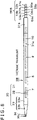
- FIG. 2A is a diagram illustrating an appearance configuration example of the electronic pen main unit 3 of this embodiment.
- FIG. 2B illustrates an electrical connection example at the joining part between the electronic pen main unit 3 of this embodiment and the fitting part 43a of the casing 2 of the electronic pen 1.
- FIG. 2C is a diagram schematically illustrating the state in which the electronic circuit inside the electronic pen main unit 3 and electronic circuit components disposed on the pen casing 2 of the electronic pen 1 are electrically connected when the electronic pen main unit 3 is fitted to the fitting part 43a.
- the electronic pen main unit 3 of the electronic pen 1 of the first embodiment is made to have a configuration that can establish compatibility with a replacement core of a ballpoint pen except the configuration of the rear end side fitted to the fitting part 43a of the pen casing 2.
- FIG. 3 depicts diagrams illustrating a configuration example of the pen tip side of the electronic pen main unit 3 of this embodiment
- FIG. 3A is a diagram illustrating the appearance thereof
- FIG. 3B is a longitudinal sectional view thereof.
- FIG. 4 depicts an exploded perspective view for explaining a configuration example of the pen tip side of the electronic pen main unit 3 of this embodiment, illustrated in FIG. 3 .
- a peripheral electrode 33 composed of an electrically-conductive component, for example, an electrically-conductive metal, is joined to the pen tip side of the main body tubular part 31 with the interposition of a tubular joining component 32, so that a casing 30 (hereinafter, referred to as a main unit casing 30) of the electronic pen main unit 3 is configured.
- the main body tubular part 31 is configured through joining of a resin pipe part 31b to the rear end side of the metal pipe part 31a on the side opposite to the pen tip side. Furthermore, in this example, for the main body tubular part 31, the peripheral electrode 33 is joined to the pen tip side of the metal pipe part 31a with the interposition of the tubular joining component 32. The tubular joining component 32 also plays a role in insulation between the metal pipe part 31a and the peripheral electrode 33. Moreover, at the rear end part of the resin pipe part 31b, a rear-end-part connector fitted to the fitting part 43a disposed in the pen casing 2 of the electronic pen 1, a connector plug 50 in this example, is disposed. Meanwhile, at the fitting part 43a of the pen casing 2, a joining connector joined to the rear-end-part connector of the electronic pen main unit 3, a connector jack 90 in this example, is disposed.
- a core body holding component 7 a writing pressure detecting unit 8 a printed board 9 on which the signal transmitting circuit is mounted, and a rechargeable capacitor 10 as an example of the power storage element for supply voltage provision are disposed in such a manner as to be lined up in the axial center direction and be housed sequentially from the pen tip side.
- This connector plug 50 includes multiple terminal parts, in this example, five terminal parts 51a, 52a, 53a, 54a, and 55a, that are electrically connected to the capacitor 10 housed in the electronic pen main unit 3 and the electronic circuit formed on the printed board 9 and are insulated from each other.
- the five terminal parts 51a, 52a, 53a, 54a, and 55a of the connector plug 50 are configured as follows.
- the terminal part 51a is composed of a conductor metal that configures a core bar at the center.
- the connector plug 50 is configured through combining of the terminal parts 52a, 53a, 54a, and 55a that each have an inner wall surface on which an insulating layer is formed and have a cylindrical shape with the bar-shaped conductor metal of this terminal part 51a in a concentric manner.
- the terminal part 51a of the conductor metal that configures the core bar at the center is set as the tip part in the axial center direction and its annular circumferential surface and tip are made to be exposed for a predetermined length in the axial center direction.
- its annular circumferential surface is made to be exposed for a predetermined length in the axial center direction. That is, the five terminal parts 51a, 52a, 53a, 54a, and 55a of the connector plug 50 are in the state in which circular annular conductor contact parts are exposed at different positions in the axial center direction.
- the terminal part 51a has a circular column shape and its annular circumferential side surface and tip part configure the conductor contact part.
- the connector plug 50 When this connector plug 50 is inserted into a fitting recess of the connector jack 90 that configures the connector for joining formed at the fitting part 43a made on the rotor 43 disposed in the hollow part of the pen casing 2 of the electronic pen 1, as illustrated in FIG. 2B , the connector plug 50 enters the state of being elastically connected to each of five contact terminals 91, 92, 93, 94, and 95 disposed in the connector jack 90.
- Each of the five contact terminals 91, 92, 93, 94, and 95 is composed of an electrically-conductive elastic metal and is electrically connected to a respective one of the electrodes 2d and 2e for charging, the side switch 2S, and the conductor band 2f that are disposed on the pen casing 2 (see FIG. 2C ).
- the terminal parts 51a, 52a, 53a, 54a, and 55a of the connector plug 50 are each electrically connected to a respective one of the electrodes 2e and 2d for charging, both ends 2Sa and 2Sb of the side switch 2S, and the conductor band 2f through the five contact terminals 91, 92, 93, 94, and 95 disposed in the connector jack 90 (diagrammatic representation of the contact terminals of the connector jack 90 is omitted in FIG. 2C ).
- the circular annular conductor contact parts of the terminal parts 51a, 52a, 53a, 54a, and 55a of the connector plug 50 are connected to the contact terminals 91, 92, 93, 94, and 95, respectively, of the connector jack 90. Therefore, even when the electronic pen main unit 3 rotates around the center line in the axial center direction, the electrical connection is always kept, and electrical non-contact can be avoided.
- the electronic circuit of the electronic pen main unit 3 becomes capable of detecting the state of the side switch 2S and can transmit information regarding the detected state of the side switch 2S with the information included in a signal sent out by a core body 35.
- the earth electrode of the electronic pen main unit 3 and the conductor band 2f of the pen casing 2 are electrically connected. Therefore, through grasping of the part of the conductor band 2f by the user, the earth electrode of the electronic pen main unit 3 can be grounded through the human body, and transmission and reception of signals from the electronic pen main unit 3 can be stably carried out.
- the peripheral electrode 33 disposed on the pen tip side of the main body tubular part 31 is made into a shape having a cylindrical shape part 33a in which the outer diameter is constant and a tapered part 33b formed into a tapered shape in such a manner as to be gradually tapered toward the pen tip side.
- the metal pipe part 31a of the main body tubular part 31 has a cylindrical shape with an outer diameter equal to an outer diameter R2 (> R1) of the cylindrical shape part 33a of the peripheral electrode 33.
- R2 2.2 millimeters is set.
- the tubular joining component 32 is composed of an insulating material, resin in this example, and is a tubular body like one illustrated in FIG. 3B .
- a ring-shaped flange part 32F that protrudes from this outer circumferential side surface in the direction orthogonal to the axial center direction is formed.
- This ring-shaped flange part 32F has a predetermined width W (see FIG. 3 ) in the axial center direction, and its end surface is flush with the main body tubular part 31 and the peripheral electrode 33 without having any step being generated and configures part of the main unit casing 30 as illustrated in FIGS. 3A and 3B . That is, the diameter of the outer circumferential part of the ring-shaped flange part 32F is selected to be equal to the outer diameter of the peripheral electrode 33 and the metal pipe part 31a of the main body tubular part 31.
- the pen tip side which is one side in the axial center direction, relative to the ring-shaped flange part 32F in this tubular joining component 32 is made into a first fitting tubular part 32a fitted to the cylindrical shape part 33a of the peripheral electrode 33, and the configuration is made in such a manner that the cylindrical shape part 33a of the peripheral electrode 33 is joined to the first fitting tubular part 32a through being press-fitted thereto until reaching the place of the ring-shaped flange part 32F.
- the rear end side in the axial center direction relative to the ring-shaped flange part 32F in the tubular joining component 32 is made into a second fitting tubular part 32b fitted to the metal pipe part 31a of the main body tubular part 31, and the configuration is made in such a manner that the metal pipe part 31a of the main body tubular part 31 is joined to the second fitting tubular part 32b through being press-fitted thereto until reaching the place of the ring-shaped flange part 32F.
- the main unit casing 30 of one tubular body is formed as illustrated in FIG. 2A and FIGS. 1A and 1B. Furthermore, the metal pipe part 31a of the main body tubular part 31 composed of an electrically-conductive material and the peripheral electrode 33 are not in contact and are in a state of being electrically isolated (insulated) from each other due to the existence of the ring-shaped flange part 32F of the tubular joining component 32.
- the hollow part 30a exists inside the main unit casing 30.
- a front cap 34 composed of an insulating material is mounted on the pen tip side of the peripheral electrode 33 of the main unit casing 30 as illustrated in FIG. 2A and FIGS. 3A and 3B .
- the front cap 34 has, on its tip side, an opening 34a (see FIG. 3B ) with a diameter larger than that of the center electrode 35 and the opening 34a communicates with the hollow part 30a of the main unit casing 30.
- the center electrode 35 is what configures a core body of the electronic pen main unit 3 of this embodiment and is composed of an electrically-conductive component, in this example, an electrically-conductive metal. Furthermore, as illustrated in FIG. 3B , this center electrode 35 is inserted into the main unit casing 30 from the opening 34a of the front cap 34, and the end part on the side opposite to the pen tip side is mounted to the core body holding component 7 attachably and detachably.
- the core body 35 and the peripheral electrode 33 that are composed of the electrically-conductive material are electrically isolated (insulated) by the front cap 34 that is the insulating material as illustrated in FIG. 3B .
- the peripheral electrode 33 is disposed to surround the rear end side relative to a tip part 35a that becomes the pen tip in the center electrode 35 as illustrated in FIG. 3B .
- the center electrode 35 will be referred to as the core body 35.
- the tapered part 33b on the pen tip side in the peripheral electrode 33 of the main unit casing 30 has a diameter that gradually becomes smaller as the position gets closer to the pen tip side.
- the pen tip side relative to a middle position in the axial center direction in the tapered part 33b is configured to be equal to or smaller than the diameter R0 of the opening 2b on the pen tip side in the pen casing 2.
- the electronic pen main unit 3 with the above configuration can be housed in the pen casing 2 by fitting its main body tubular part 31 to the fitting part 43a of the rotor 43 of the knock cam mechanism unit 4. Furthermore, in the electronic pen 1 of this embodiment, the user presses down the end part 42a of the knock bar 42 when using the electronic pen 1 with a position detecting device. Thereupon, in the electronic pen 1, the state is made in which, as illustrated in FIG. 1B , the tip part 35a of the core body 35, the front cap 34, and a part of the pen tip side of the tapered part 33b of the peripheral electrode 33 protrude to the external from the opening 2b of the pen casing 2.
- the state can be made in which the whole of the electronic pen main unit 3 is housed in the hollow part 2a of the pen casing 2 as illustrated in FIG. 1A .
- the whole of the electronic pen main unit 3 is housed in the hollow part 2a of the pen casing 2, and the tip part 35a of the core body 35 of the electronic pen main unit 3 enters the state of being protected by the pen casing 2.
- a board holder 300 in which the printed board 9 is placed on a board placement pedestal 301 is housed in the hollow part 30a of the main unit casing 30.
- the board holder 300 is composed of an insulating resin and has a writing pressure detecting unit holding part 302 for housing and holding the writing pressure detecting unit 8 on the side opposite to the side of the board placement pedestal 301 in the longitudinal direction that is the axial center direction of the electronic pen main unit 3.
- the board holder 300 is made to have a configuration in which the writing pressure detecting unit holding part 302 and the board placement pedestal 301 are continuous in the longitudinal direction that is the axial center direction of the electronic pen main unit 3 when the board holder 300 is housed in the hollow part of the main unit casing 30.
- the writing pressure detecting unit holding part 302 is made into a cylindrical shape having a hollow part inside which multiple parts of the writing pressure detecting unit 8 are housed.
- the board placement pedestal 301 is made into a shape that is a boat shape on which the printed board 9 is placed to be held, and is like one obtained by cutting a tubular body by substantially half along the axial center direction.
- the board holder 300 is housed in the main unit casing 30 in such a manner that the writing pressure detecting unit holding part 302 is set on the pen tip side. Furthermore, the configuration is made in such a manner that the core body holding component 7 that is fitted to the core body 35 and holds the core body 35 is joined to the writing pressure detecting unit 8 held by this writing pressure detecting unit holding part 302, and the pressure (writing pressure) applied to the core body 35 is transmitted to the writing pressure detecting unit 8.
- the board holder 300 is subjected to position restriction in such a manner as not to move in the axial center direction in the main unit casing 30 through fitting and joining of the writing pressure detecting unit holding part 302 to the second fitting tubular part 32b of the tubular joining component 32 in the axial center direction as illustrated in FIG. 3B .
- the metal pipe part 31a of the main body tubular part 31 composed of the electrically-conductive material is electrically connected to the copper foil pattern of the earth line of the printed board 9.
- a circuit part that is composed of the signal transmitting circuit that generates signals to be sent out from the core body 35 and the peripheral electrode 33, an IC (Integrated Circuit) 100 (see FIGS. 3A and 3B ) that configures a control circuit that controls transmission of the signals from the signal transmitting circuit to the core body 35 and the peripheral electrode 33, and peripheral circuit part thereof.
- a charging circuit of the capacitor 10 is included in the peripheral circuit part although diagrammatic representation is omitted.
- the charging circuit of the capacitor 10 may be disposed outside the electronic pen 1.
- the core body holding component 7 that holds the core body 35 through fitting is composed of an electrically-conductive elastic component 71, a core body holder 72, a coil spring 73, and a conductor terminal component 74.
- the core body holding component 7 also plays a role as a transmitting component of the writing pressure applied to the core body 35 for the writing pressure detecting unit 8.
- the core body 35 is fitted into the core body holder 72 composed of an electrically-conductive material through the electrically-conductive elastic component 71 and is thereby joined to the core body holder 72 to be held.
- the electrically-conductive elastic component 71 is composed of, for example, electrically-conductive rubber and is formed into a cylindrical shape having a through-hole 71a into which the end part of the core body 35 on the side opposite to the tip part 35a is fitted.
- the core body holder 72 is composed of an electrically-conductive material, for example, SUS (Steel Special Use Stainless), and is an object in which a housing fitting part 721 having a recessed hole 721a in which the electrically-conductive elastic component 71 is housed and fitted and a bar-shaped part 722 fitted into a holding component 83 to be described later in the writing pressure detecting unit 8 are monolithically formed.
- SUS Step Special Use Stainless
- the configuration is made in such a manner that the pressure (writing pressure) applied to the core body 35 is transmitted to the writing pressure detecting unit 8 through fitting of a tip part 722a of the bar-shaped part 722 of the core body holder 72 into the holding component 83 of the writing pressure detecting unit 8 held by the writing pressure detecting unit holding part 302.
- the configuration is made in such a manner that the core body holder 72 is always biased toward the side of the core body 35 against the board holder 300 by the coil spring 73 as an example of an elastic component composed of an electrically-conductive material such as an electrically-conductive metal.
- the coil spring 73 configures, with the conductor terminal component 74, a component for electrical connection for transmitting a signal from the IC 100 disposed on the printed board 9 to the core body 35.
- a transmission signal generated by the signal transmitting circuit configured on the printed board 9 is supplied to the core body 35 through the component for electrical connection including this coil spring 73 and the conductor terminal component 74.
- the conductor terminal component 74 composed of a material having electrical conductivity, for example, SUS, is mounted in such a manner as to cover the side of an opening 302a into which the bar-shaped part 722 of the core body holder 72 is inserted as illustrated in FIG. 4A .
- this conductor terminal component 74 has an abutting plate part 741 that covers the side of the opening 302a of the writing pressure detecting unit holding part 302 of the board holder 300 and has a through-hole 741a in which the bar-shaped part 722 of the core body holder 72 is inserted.
- an extending part 742 that extends to the part of the board placement pedestal 301 is disposed across the part of the writing pressure detecting unit holding part 302 of the board holder 300.
- a terminal part 742a at the tip of the extending part 742 that extends from the conductor terminal component 74 abuts against a conductor on the back surface side of the printed board 9 placed on the board placement pedestal 301 of the board holder 300 and is soldered thereto, for example. Due to this, the conductor terminal component 74 and the signal transmitting circuit disposed on the printed board 9 are electrically connected.
- the bar-shaped part 722 of the core body holder 72 into which the electrically-conductive elastic component 71 is fitted is inserted into the hollow part of the writing pressure detecting unit holding part 302 of the board holder 300 through the through-hole 741a of the abutting plate part 741 of the conductor terminal component 74 and is fitted into the writing pressure detecting unit holding part 302 in the state in which the coil spring 73 is interposed.
- the inner diameter of the coil spring 73 is set larger than the outer shape of the bar-shaped part 722 of the core body holder 72.
- the coil spring 73 elastically gets contact with the core body holder 72 and abuts against and elastically gets contact with the abutting plate part 741 of the conductor terminal component 74.
- the coil spring 73 is composed of an electrically-conductive material, and the electrically-conductive elastic component 71 and the core body holder 72 have electrical conductivity.
- the signal transmitting circuit disposed on the printed board 9 and the electrically-conductive elastic component 71 fitted into the core body holder 72 are electrically connected through the conductor terminal component 74. Therefore, fitting of the core body 35 into the electrically-conductive elastic component 71 makes the state in which a signal from the signal transmitting circuit disposed on the printed board 9 is supplied to the core body 35.
- the writing pressure detecting unit 8 is housed in the writing pressure detecting unit holding part 302, and the configuration is made as illustrated in FIG. 3B , thereby configuring a module for writing pressure detection. Furthermore, the core body 35 is joined to this module for writing pressure detection through the core body holder 72. Due to this, the writing pressure applied to the tip part 35a of the core body 35 is detected by the writing pressure detecting unit 8 of the module for writing pressure detection. In this case, the module for writing pressure detection detects the writing pressure through movement of a portion of the parts of the writing pressure detecting unit 8 that configures the module in the axial center direction together with the core body 35 and the core body holder 72 according to the writing pressure applied to the tip part 35a of the core body 35.
- the writing pressure detecting unit 8 of this example is a case in which a capacitance-variable capacitor whose capacitance changes according to the writing pressure applied to the core body 35 is used, and is composed of multiple parts, a dielectric 81, a terminal component 82, the holding component 83, an electrically-conductive component 84, and an elastic component 85, as illustrated in FIG. 3B .
- the core body 35 is press-fitted into the through-hole 71a of the electrically-conductive elastic component 71 fitted into the core body holder 72. Due to this, the core body 35 is firmly held with respect to the core body holder 72 by the electrically-conductive elastic component 71 as described above.
- the core body 35 can be pulled out in the direction toward the side of the tip part 35a from the state of being fitted into the core body holder 72 and being held and can be replaced as described above.
- this electronic pen main unit 3 when a pressure is applied to the tip part 35a of the core body 35, the core body 35 is displaced toward the rear end side in the axial center direction according to the pressure. Due to this displacement, the holding component 83 in the writing pressure detecting unit holding part 302 is displaced toward the side of the dielectric 81 against an elastic biasing force of the elastic component 85. As a result, the electrically-conductive component 84 fitted into the holding component 83 is displaced toward the side of the dielectric 81, so that the distance between the electrically-conductive component 84 and the dielectric 81 and the contact area between the electrically-conductive component 84 and the dielectric 81 change according to the pressure applied to the core body 35.
- the capacitance of a capacitance-variable capacitor formed between the terminal component 82 that configures a first electrode and the electrically-conductive component 84 that configures a second electrode changes according to the pressure applied to the core body 35.
- This change in the capacitance of the capacitance-variable capacitor is detected by the IC 100 disposed on the printed board 9, and the writing pressure is detected.
- the writing pressure detecting unit 8 is not limited to one with the above-described configuration.
- a capacitance-variable capacitor includes a semiconductor chip formed of a MEMS (Micro Electro Mechanical Systems) element (refer to patent document ( Japanese Patent Laid-open No. 2013-161307 ), for example) may be used.
- MEMS Micro Electro Mechanical Systems
- a recessed groove (diagrammatic representation is omitted) is formed from the first fitting tubular part 32a to the second fitting tubular part 32b by passing through the lower part of the ring-shaped flange part 32F in the direction along the axial center direction of the tubular joining component 32.
- a recessed groove (diagrammatic representation is omitted) continuous with the recessed groove of the second fitting tubular part 32b is formed also in the circumferential side surface of the writing pressure detecting unit holding part 302 of the board holder 300.
- a connection terminal conductor 11 composed of an electrically-conductive material, in this example, an electrically-conductive metal, is disposed.
- an end part 11a of the connection terminal conductor 11 disposed in the recessed groove on the side of the first fitting tubular part 32a of the tubular joining component 32 is disposed in such a manner that at least part of the end part 11a slightly bulges out relative to the outer circumferential surface of the first fitting tubular part 32a.
- the depth of the recessed groove of the part of the end part 11a is set to a depth that allows the end part 11a to be elastically pressed downward when the end part 11a is pressed down from above.
- the configuration is made in such a manner that the end part 11a of the connection terminal conductor 11 surely gets contact with the inner wall of the peripheral electrode 33 and the state in which the peripheral electrode 33 and the connection terminal conductor 11 are electrically connected is made when the peripheral electrode 33 is fitted to the first fitting tubular part 32a of the tubular joining component 32. Furthermore, an end part 11b that extends to the side of the printed board 9 of the connection terminal conductor 11 is electrically connected to the side of a back surface 9b of the printed board 9 as illustrated in FIG. 3B . Although diagrammatic representation is omitted, the end part 11b of the connection terminal conductor 11 is electrically connected to the circuit part on the front surface side of the printed board 9 via a through-hole.
- the depth of the recessed groove in which the connection terminal conductor 11 is disposed is set to a depth with which the connection terminal conductor 11 does not get contact with the metal pipe part 31a when the metal pipe part 31a of the main body tubular part 31 is fitted to the second fitting tubular part 32b.
- an insulator may be interposed between the connection terminal conductor 11 and the metal pipe part 31a.
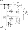
- a control circuit 101 includes the IC 100 disposed on the printed board 9. Furthermore, to this control circuit 101, a signal transmitting circuit 102 and a signal receiving circuit 103 are connected and a variable-capacitance capacitor 8C including the writing pressure detecting unit 8 is connected. A resistor 8R is connected in parallel to the variable-capacitance capacitor 8C.
- a signal output end of the signal transmitting circuit 102 is connected to the core body 35 through a switch circuit 104.
- the interposition of the conductor terminal component 74, the core body holder 72, and the electrically-conductive elastic component 71 between the core body 35 and the switch circuit 104 is as described above.
- the signal output end of the signal transmitting circuit 102 is connected to a terminal S of a changeover switch circuit 105.
- a movable terminal M of this changeover switch circuit 105 is connected to the peripheral electrode 33.
- the connection terminal conductor 11 is interposed between the peripheral electrode 33 and the changeover switch circuit 105.
- a terminal R of the changeover switch circuit 105 is connected to an input end of the signal receiving circuit 103. Furthermore, a terminal G of the changeover switch circuit 105 is connected to an earth electrode (ground electrode).
- control circuit 101 supplies the switch circuit 104 with a control signal SW1 that carries out on/off-control of the switch circuit 104. Furthermore, the control circuit 101 supplies the changeover switch circuit 105 with a changeover control signal SW2 to switch which of the terminal S, the terminal R, and the terminal G the movable terminal M is to be connected to.
- the voltage of the capacitor 10 is supplied to each of the control circuit 101, the signal transmitting circuit 102, the signal receiving circuit 103, the switch circuit 104, and the changeover switch circuit 105 as a supply voltage.
- the signal receiving circuit 103 receives a signal received by the peripheral electrode 33 through capacitive coupling (electric field coupling) with a position detecting sensor of a position detecting device and executes processing of demodulation and so forth according to the received signal to send a signal of the processing result to the control circuit 101.
- the control circuit 101 analyzes the signal from the signal receiving circuit 103 and determines the specifications of the position detecting device of the counterpart. In addition, the control circuit 101 settles the timing at which interaction of a signal is carried out with the position detecting sensor of the position detecting device of the counterpart. Furthermore, the control circuit 101 controls the format of a signal to be output from the signal transmitting circuit 102 in such a manner that the format becomes what matches the specifications of the position detecting device of the counterpart and carries out interaction with the position detecting sensor at the settled timing.
- the signal transmitting circuit 102 outputs, under control of the control circuit 101, a signal including a signal for position detection (burst signal) with a predetermined frequency for position detection in the position detecting device and writing pressure information according to the writing pressure detected by the writing pressure detecting unit 8. Furthermore, the signal transmitting circuit 102 outputs also a signal for detection of a tilt angle of the electronic pen 1. That is, the signal transmitting circuit 102 sends out the burst signal for position detection and the burst signal for detection of the tilt angle of the electronic pen 1 under control by the control circuit 101.
- a signal for position detection burst signal
- burst signal burst signal
- the control circuit 101 carries out operation of detecting the writing pressure on the basis of the capacitance of the variable-capacitance capacitor 8C including the writing pressure detecting unit 8.
- the control circuit 101 first charges the variable-capacitance capacitor 8C to the fully-charged state and thereafter stops the charging to thereby set the variable-capacitance capacitor 8C to the state of being discharged through the resistor 8R. Then, the control circuit 101 measures the time from the discharging start timing to the timing when the voltage across the variable-capacitance capacitor 8C becomes a predetermined voltage set in advance and detects the capacitance of the variable-capacitance capacitor 8C at the time from the time.
- the capacitance of the variable-capacitance capacitor 8C corresponds to the writing pressure applied to the core body 35 at the time and detects the writing pressure on the basis of the detected capacitance.
- the control circuit 101 converts the detected writing pressure to a digital signal of multiple bits in this example and controls the signal transmitting circuit 102 to output writing pressure information according to this digital signal from this signal transmitting circuit 102.
- a supply voltage Vcc stored in the capacitor 10 is supplied to each of the control circuit 101, the signal transmitting circuit 102, the signal receiving circuit 103, the switch circuit 104, and the changeover switch circuit 105.
- a charging circuit 106 of the capacitor 10 is disposed on the printed board 9 and is connected to the terminals 52a and 51a of the connector plug 50 to which the electrodes 2d and 2e for charging are connected. Therefore, although diagrammatic representation is omitted, when the electrodes 2d and 2e for charging are connected to an AC power supply through an adapter for charging, the capacitor 10 is charged by the charging circuit 106.
- the side switch 2S disposed on the pen casing 2 is connected to the control circuit 101 through the terminals 53a and 54a of the connector plug 50.
- the control circuit 101 determines the on- and off-states of the side switch 2S and generates information regarding the determined state of the side switch 2S to transmit the generated information regarding the state of the side switch 2S to the position detecting device through the signal transmitting circuit 102.
- the earth electrode (ground conductor) of the electronic pen main unit 3 is connected to the conductor band 2f through the terminal 55a of the connector plug 50.
- FIG. 6 is a block diagram for explaining a configuration example of a reception processing circuit of a signal from the electronic pen 1 in a position detecting device 200 of a capacitive system.
- the position detecting device 200 of this example is composed of a position detecting sensor 210 and a pen detecting circuit 220 connected to this position detecting sensor 210.
- the position detecting sensor 210 is composed of a first conductor group in which multiple first conductors 211 Y 1 , 211 Y 2 , ⁇ , 211 Y m (m is an integer equal to or larger than 1) that extend along the horizontal direction (X-axis direction) are disposed in a Y-axis direction in parallel separately from each other by a predetermined interval and a second conductor group in which multiple second conductors 212Xi, 212X 2 , ⁇ , 212X n (n is an integer equal to or larger than 1) that extend along the vertical direction (Y-axis direction) are disposed in the X-axis direction in parallel separately from each other by a predetermined interval.
- the conductors when there is no need to distinguish the multiple first conductors of the first conductor group and the multiple second conductors of the second conductor group from one another, the conductors will be referred to as the first conductor 211Y and the second conductor 212X.
- the pen detecting circuit 220 is composed of a selection circuit 221 used as an input-output interface with the position detecting sensor 210, an amplification circuit 222, a band-pass filter 223, a detection circuit 224, a sample-hold circuit 225, an AD (Analog to Digital) conversion circuit 226, and a control circuit 227.
- the selection circuit 221 selects one conductor 211Y or 212X from the first conductor group and the second conductor group on the basis of a control signal from the control circuit 227.
- the conductor selected by the selection circuit 221 is connected to the amplification circuit 222, and a signal from the electronic pen 1 (electronic pen main unit 3 thereof) is detected by the selected conductor and is amplified by the amplification circuit 222.
- the output of this amplification circuit 222 is supplied to the band-pass filter 223, and only the component of the frequency of the signal transmitted from the electronic pen 1 is extracted.
- An output signal of the band-pass filter 223 is detected by the detection circuit 224 and an output signal thereof is supplied to the sample-hold circuit 225 and is sampled and held by a sampling signal from the control circuit 227. Thereafter, the signal is converted to a digital value by the AD conversion circuit 226. Digital data from the AD conversion circuit 226 is read by the control circuit 227 and is processed.
- the control circuit 227 sends out a control signal to each of the sample-hold circuit 225, the AD conversion circuit 226, and the selection circuit 221. In addition, the control circuit 227 calculates position coordinates on the position detecting sensor 210 indicated by the electronic pen 1 from the digital data from the AD conversion circuit 226 and detects writing pressure information.
- control circuit 227 detects a tilt angle of the electronic pen 1 in a manner described below. A method of the detection of the tilt angle of the electronic pen 1 in this position detecting device 200 will be described with reference to FIG. 7 .
- the region OBa in which capacitive coupling is made between the tip part 35a of the core body 35 and the position detecting sensor 210 in the position detection period Ta substantially remains the region of the true circle as illustrated in FIG. 7E .
- the region OBb in which capacitive coupling is made between the peripheral electrode 33 and the position detecting sensor 210 in the tilt detection period Tb becomes a region of an elliptical shape that is according to the tilt angle and extends long in the direction of the tilt as illustrated in FIG. 7F .
- the magnitude of the tilt angle of the electronic pen 1 can be detected from the length in the major axis direction regarding the elliptical shape of the region OBb illustrated in FIG. 7F . Furthermore, the direction of the tilt of the electronic pen 1 can be detected by detecting the major axis direction of the elliptical shape of the region OBb with the indicated position of the electronic pen 1 illustrated in FIG. 7E being deemed as the point of origin.
- a signal with the same frequency as the signal supplied to the core body 35 is used for the peripheral electrode 33 used for detecting the tilt angle.
- the frequency of the signal supplied to the core body 35 and the frequency of the signal supplied to the peripheral electrode 33 may be made different.
- the signal from the core body 35 and the signal from the peripheral electrode 33 can be distinguished in the position detecting device 200.
- the configuration may be made in such a manner that the signal from the core body 35 and the signal from the peripheral electrode 33 are simultaneously sent out to the position detecting sensor 210 instead of carrying out the position detection period Ta and the tilt detection period Tb in a time-sharing manner as described above.
- the connector plug 50 of the electronic pen main unit 3 and the connector jack 90 of the fitting part 43a are joined. Due to this, the electronic circuit inside the electronic pen main unit 3 connected to the connector plug 50 of the electronic pen main unit 3 and electronic circuit components such as the electrodes 2d and 2e for charging, the side switch 2S, and the conductor band 2f on the pen casing 2 connected to the connector jack 90 of the pen casing 2 are electrically connected.
- the connector jack 90 is disposed at the fitting part 43a moved by the knock cam mechanism unit 4 as the movement mechanism disposed in the pen casing 2, and the connector plug 50 is disposed at the rear end part of the electronic pen main unit 3 fitted to this fitting part. Therefore, the electrical connection is always secured even when the electronic pen main unit 3 moves in the axial center direction in the pen casing 2.
- the circular annular conductor contact parts of the terminal parts 51a, 52a, 53a, 54a, and 55a of the connector plug 50 are connected to the contact terminals 91, 92, 93, 94, and 95, respectively, of the connector jack 90. Therefore, even when the electronic pen main unit 3 rotates around the center line in the axial center direction, the electrical connection is always kept, and electrical non-contact can be avoided.
- the electronic pen 1 of this first embodiment in use of the electronic pen 1 in which the pen tip side of the electronic pen main unit 3 protrudes to the external from the opening 2b of the pen casing 2 of the electronic pen 1, not only the tip part 35a of the core body 35 but also part of the tapered part 33b on the pen tip side in the peripheral electrode 33 protrudes from the opening 2b of the pen casing 2.
- the distance between not only the tip part 35a of the core body 35 and the input surface of the position detecting sensor 210 but also the tapered part 33b on the pen tip side in the peripheral electrode 33 becomes short, and capacitive coupling (electric field coupling) between both the two becomes strong.
- the pen tip side of the peripheral electrode 33 is made into the tapered part 33b, the cross-sectional area of the tip part thereof on the pen tip side is small, and the electric field coupling is made more strongly with the position detecting sensor 210.
- the electronic pen 1 of this first embodiment can strongly make electric field coupling with the position detecting sensor 210 even when being made thinner.
- the position detecting device 200 it becomes possible to detect sensing of the position indicated by the electronic pen 1 with high sensitivity.
- a signal from the position detecting device 200 is received by the peripheral electrode 33, and the electronic pen main unit 3 starts transmission of a signal at a timing ordered by the received signal. This allows the position detecting device to wait for reception of the signal from the electronic pen main unit 3 while predicting transmission of the signal from the electronic pen main unit 3 of the electronic pen 1, and favorable operation can be implemented even with the electric field coupling with smaller coupling strength compared with the electromagnetic induction system.
- the connector plug 50 as an example of the rear-end-part connector of the electronic pen main unit 3 and the connector jack 90 as an example of the connector for joining at the fitting part 43a of the pen casing 2 are one example of the rear-end-part connector of the electronic pen main unit and the connector for joining at the fitting part of the pen casing, and the fitting configuration is not limited thereto.
- FIG. 8 illustrates another example of the rear-end-part connector of the electronic pen main unit and the connector for joining at the fitting part of the pen casing.
- an electronic pen main unit 3B of this example only the configuration of the rear-end-part connector is different from the example of FIG. 2A , and the others are similar to the electronic pen main unit 3 of the above-described first embodiment.
- the electronic pen main unit 3B a constituent part similar to that of the electronic pen main unit 3 is given the same reference numeral, and detailed description thereof is omitted.
- a connector plug 50B as an example of the rear-end-part connector is disposed at the rear end part of the resin pipe part 31b of the main body tubular part 31.
- This connector plug 50B is what has a configuration similar to that of a pin plug for audio (for example, 5-pole pin plug with a noise cancelling function).
- five terminal parts 51b, 52b, 53b, 54b, and 55b are in the state in which circular annular conductor contact parts with the same diameter are exposed at positions different in the axial center direction.
- the terminal part 51b at the tip of the five terminal parts 51b, 52b, 53b, 54b, and 55b is made into a tip terminal.
- the middle three terminal parts 52b, 53b, and 54b are each made into a ring terminal insulated from other terminal parts by insulating rings 56a, 56b, 56c, and 56d.
- the terminal part 55b on the root side of the electronic pen main unit 3B is made into a sleeve terminal.
- a connector jack as an example of the connector for joining that is joined to the connector plug 50B of the electronic pen main unit 3B of this example and is disposed at the fitting part 43a of the pen casing 2 includes five contact terminals that get contact with each of the circular annular conductor contact parts of the five terminal parts 51b, 52b, 53b, 54b, and 55b and form an electrical connection similarly to FIG. 2B although diagrammatic representation is omitted here.
- terminal parts 51b, 52b, 53b, 54b, and 55b of the connector plug 50B are each electrically connected to a respective one of the electrodes 2e and 2d for charging, both ends 2Sa and 2Sb of the side switch 2S, and the conductor band 2f on the pen casing 2 through the five contact terminals disposed in the connector jack.
- the circular annular conductor contact parts of the terminal parts 51b, 52b, 53b, 54b, and 55b of the connector plug 50B are connected to a respective one of the five contact terminals of the connector jack of the fitting part 43a. Therefore, even when the electronic pen main unit 3B rotates around the center line in the axial center direction, the electrical connection is always kept, and electrical non-contact can be avoided.
- the rear-end-part connector of the rear end part on the side opposite to the pen tip side in the main body tubular part 31 of the electronic pen main unit 3 or the electronic pen main unit 3B is made to have a configuration of a connector plug
- the connector for joining at the fitting part 43a of the pen casing 2 is made to have a configuration of a connector jack.
- the rear-end-part connector of the electronic pen main unit 3 or the electronic pen main unit 3B may be made to have a configuration of a connector jack
- the connector for joining at the fitting part 43a of the pen casing 2 may be made to have a configuration of a connector plug.
- An electronic pen of this second embodiment is a modification example of the first embodiment.
- only one electronic pen main unit 3 or electronic pen main unit 3B is housed in the pen casing 2 of the electronic pen 1.
- multiple electronic pen main units are housed in a pen casing of an electronic pen.
- a knock mechanism as an example of the movement mechanism, one of the multiple electronic pen main units is selected, and the tip of the pen tip part of the selected electronic pen main unit is protruded from an opening of the casing on the pen tip side and is used.
- the electronic pen main unit 3 or the electronic pen main unit 3B of the electronic pen 1 of the first embodiment is made to have a configuration that can establish compatibility with a replacement core of a ballpoint pen except the configuration of the rear end side fitted to the fitting part 43a of the pen casing 2.
- a multi-color ballpoint pen in which replacement cores different in the ink color are mounted exists.
- This second embodiment provides an electronic pen including housing the electronic pen main unit 3 in a casing with a configuration similar to that of the casing of this multi-color ballpoint pen.
- FIG. 9 is a configuration diagram illustrating the appearance of an electronic pen 1M of this second embodiment. Also in this example of FIG. 9 , a pen casing 2M of the electronic pen 1M is composed of a transparent synthetic resin and is illustrated to be in the state in which the inside thereof is visible in a see-through manner.
- the pen casing 2M of the electronic pen 1M has almost the same configuration as a casing and a knock mechanism of a commercially-available knock-type multi-color ballpoint pen.
- a configuration in which electrodes 2Md and 2Me for charging, a side switch 2MS, and a conductor band 2Mf are disposed on the pen casing 2M and a configuration of a fitting part to which an electronic pen main unit 3AES is fitted in the knock mechanism are different from the casing and the knock mechanism of the commercially-available knock-type multi-color ballpoint pen.
- one electronic pen main unit 3AES is housed and replacement cores of ballpoint pens of two colors, for example, a replacement core 6R of a red ballpoint pen and a replacement core 6B of a black ballpoint pen, are housed.
- the electronic pen main unit 3AES is configured similarly to the electronic pen main unit 3 or the electronic pen main unit 3B of the first embodiment except that the electronic pen main unit 3AES is configured with the same dimensions as the replacement core of the multi-color ballpoint pen, and includes a rear-end-part connector with a configuration similar to that of the connector plug 50 or 50B, for example, on the rear end side of the main body tubular part 31.
- the knock mechanism of the electronic pen 1M is equipped with knock bars 42AES, 42R, and 42B to which the electronic pen main unit 3AES and the replacement cores 6R and 6B of the red and black ballpoint pens, respectively, are fitted.
- a fitting part 43AES disposed on the knock bar 42AES is made to have a configuration including a joining connector joined to the rear-end-part connector configured at the rear end part of the electronic pen main unit 3AES similarly to the fitting part 43a of the knock cam mechanism unit 4 in the first embodiment. Therefore, the electrodes 2Md and 2Me for charging, the side switch 2MS, and the conductor band 2Mf are electrically connected to five terminals of the connector for joining.
- the fitting parts 43R and 43B of the knock bars 42R and 42B are made into fitting parts of a multi-color ballpoint pen.
- any of the knock bars 42AES, 42R, and 42B is moved by sliding toward the pen tip side, and thereby the pen tip side of the electronic pen main unit 3AES or either the replacement core 6R or 6B of the red or black ballpoint pen protrudes from an opening 2Ma of the pen casing 2M. Furthermore, by the slide movement of the knock bar 42AES toward the pen tip side, the tip part 35a of the core body 35 and a part of the peripheral electrode 33 of the electronic pen main unit 3AES protrude to be caused to make electric field coupling with a position detecting sensor of a position detecting device.
- the electronic pen main unit 3AES and the replacement cores 6R and 6B of ballpoint pens are housed in the pen casing 2M, and therefore the axial center direction of the electronic pen main unit 3AES deviates from the opening 2Ma of the pen casing 2M.
- the electronic pen main unit 3AES pushed out slightly bends with respect to the fitting part 43AES of the pen casing 2M.
- the main body tubular part 31 of the electronic pen main unit 3AES of this embodiment includes the resin pipe part 31b. Therefore, due to the elasticity of this resin pipe part 31b, it is possible to deal with the bending of the electronic pen main unit 3 at the time of letting-out of the tip part of the electronic pen main unit 3.
- the length of the resin pipe part 31b in the axial center direction be adjusted to a length with which the bending at the time of letting-out of the tip part of the electronic pen main unit 3AES can be favorably absorbed by the resin pipe part 31b.
- the fitting part 43AES of the knock bar 42AES in the three knock bars 42AES, 42R, and 42B is made to have a configuration including a conductor to which the electronic pen main unit 3 or the electronic pen main unit 3B can be fitted.
- two or all of the fitting parts of the three knock bars 42AES, 42R, and 42B may be made into ones for the electronic pen main unit 3 or the electronic pen main unit 3B, and the fitting parts may be made into ones with a configuration including a conductor.
- an IC and a peripheral circuit thereof for implementing a function of transmitting its own identification information to a position detecting device be disposed in the main unit casing 30 in which electronic circuit components are disposed.
- the position detecting device used with the electronic pen main unit 3 or the electronic pen main unit 3B has a function of receiving and determining the identification information transmitted from each of the electronic pen main units 3 or the electronic pen main units 3B. Furthermore, the position detecting device determines the difference among the electronic pen main units 3AES fitted to the fitting parts 43AES, 43R, and 43B and implements functions assigned to the respective ones. For example, in a case in which all of the fitting parts of the three knock bars 42AES, 42R, and 42B are made into ones for the electronic pen main unit 3 or the electronic pen main unit 3B, to the electronic pen main unit fitted to the fitting part 43R, a function of representing a writing locus (character or figure) displayed according to the indicated position thereof by red can be assigned.
- a function of representing a writing locus displayed according to the indicated position thereof by black can be assigned.
- a function of erasing a writing locus input through indication previously according to the indicated position thereof can be assigned.
- the functions assigned to the electronic pen main units are not only the display color of the locus according to the indicated position as in this example and may be the kinds of displayed line, such as the thickness of a locus, a solid line, a dotted line, and a one-dot chain line.
- the electrodes 2Ed and 2Ee for charging and the conductor band 2Mf can be made common to these multiple electronic pen main units 3 or 3B.
- the side switch 2MS may be made common to the multiple electronic pen main units 3 or 3B housed in the pen casing 2M, or multiple side switches may be disposed on the pen casing 2M corresponding to a respective one of the multiple electronic pen main units 3 or 3B housed in the pen casing 2M.
- the second embodiment is the example including the three knock bars, the number of knock bars may be two or may be four or more.
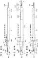
- FIG. 10 other embodiments of the electronic pen main unit are illustrated.
- FIG. 10A illustrates a modification example of another example of the electronic pen main unit 3B illustrated in FIG. 8 in the above-described first embodiment.
- This example is an example configured in consideration of common use with a replacement core of a ballpoint pen similarly to the second embodiment.
- description of an electronic pen main unit 3 C of this embodiment a constituent part similar to that of the above-described electronic pen main unit 3B is given the same reference numeral, and detailed description thereof is omitted.
- a peripheral electrode 33C with a different shape from the peripheral electrode 33 of the electronic pen main unit 3B of the first embodiment is used.
- the peripheral electrode 33C of the electronic pen main unit 3C of this embodiment is made into a tubular shape whose outer diameter is constant in the axial center direction, and the outer diameter is set to a diameter R1 smaller than the diameter of the opening 2b (see FIG. 1 ) of the pen casing 2 of the electronic pen.
- a tubular joining component 32C that joins the peripheral electrode 33C to the main body tubular part 31 is configured in conformity to the configuration of the peripheral electrode 33C in such a manner that the peripheral electrode 33C can be joined to the main body tubular part 31 with the interposition of a ring-shaped flange part 32CF.
- a front cap 34C is also configured with change in conformity to the configuration of the peripheral electrode 33C. The others are made to have a configuration similar to that of the electronic pen main unit 3 of the first embodiment.
- the connector plug 50B as an example of the rear-end-part connector is disposed in this example similarly to the electronic pen main unit 3B. Furthermore, the electronic pen main unit 3 C is fitted to the fitting part 43a of the pen casing 2 of the electronic pen 1 and the connector plug 50B as an example of the rear-end-part connector is electrically connected to a connector jack as an example of the connector for joining at the fitting part 43a.
- the same operation and effects as the electronic pen 1 of the first embodiment can be obtained.
- the core body 35, the front cap 34C, and a part of the peripheral electrode 33C on the pen tip side protrude to the external from an opening of a casing 2C of the electronic pen illustrated by dotted lines in FIG. 10A .
- the cylindrical part with the constant outer diameter in the peripheral electrode 33C is located at the part of opening of the casing 2C. Therefore, by adjusting the outer diameter of the cylindrical part of this peripheral electrode 33C, the pen tip side of the electronic pen main unit 3C can be easily kept from involving a backlash in the opening of the casing 2C.
- FIG. 10B also illustrates a modification example of another example of the electronic pen main unit 3B illustrated in FIG. 8 in the above-described first embodiment.
- Parts of a main body tubular part 31D and a tubular joining component 32D of an electronic pen main unit 3D of this embodiment are different from the above-described electronic pen main unit 3B, and the other part is made into a similar configuration.
- a constituent part similar to that of the electronic pen main unit 3B is given the same reference numeral and detailed description thereof is omitted.
- the main body tubular part 31D of the electronic pen main unit 3D of this embodiment has an outer diameter R3 larger than the outer diameter R2 of the main body tubular part 31 of the above-described electronic pen main unit 3B. Furthermore, the inner diameter of the main body tubular part 31D of the electronic pen main unit 3D of this embodiment is set to a diameter larger than the inner diameter of the main body tubular part 31 of the electronic pen main unit 3 of the first embodiment.
- the tubular joining component 32D that joins the peripheral electrode 33 to the main body tubular part 3 ID is configured in conformity to the configuration of the main body tubular part 31D in such a manner that the peripheral electrode 33 can be joined to the main body tubular part 31D with the interposition of a ring-shaped flange part 32DF.
- the main body tubular part 31D of the electronic pen main unit 3D of this embodiment includes a hollow part with a large space. Furthermore, in the electronic pen main unit 3D of this embodiment, by use of the space of the large hollow part of this main body tubular part 31D, the configuration is made in such a manner that a primary cell (battery) 10BT is housed in the hollow part as illustrated in FIG. 10B instead of the capacitor 10 as the power storage element used in the above-described electronic pen main unit 3B.
- the other electronic circuit components in the main body tubular part 31D are housed in the main body tubular part 31D similarly to the first embodiment, and the necessary supply voltage to the respective parts is supplied from the primary cell 10BT incorporated in the main body tubular part 31D. Therefore, the electrodes 2d and 2e for charging do not need to be disposed on the pen casing 2D of the electronic pen 1 using the electronic pen main unit 3D of this embodiment.
- the main body tubular part 3 ID of the electronic pen main unit 3D of this embodiment is formed of a metal pipe.
- a component 31DE in which a connector plug 50B' as an example of the rear-end-part connector is formed on a resin base 31Da is mounted attachably and detachably.
- the configuration is made in such a manner that the primary cell 10BT housed in the main body tubular part 31D can be replaced through removal of the component 31DE.
- the casing of the electronic pen that houses the electronic pen main unit 3D of this embodiment is set to a diameter larger than that of the casing 2 of the electronic pen of the above-described first embodiment.
- the other configuration of the casing of the electronic pen is made similar to the above-described embodiment and includes a movement mechanism such as a knock cam mechanism or knock mechanism. At a fitting part moved by the movement mechanism, a connector jack to which the connector plug 50B' of the rear end part of the electronic pen main unit 3D is joined and that is electrically connected to a side switch and the conductor band 2f is disposed.
- a secondary cell or a power storage element such as a capacitor may be disposed instead of disposing the primary cell 10BT in the hollow part of the main body tubular part 31D.
- the configuration of the rear-end-part connector of the main body tubular part 31D of the electronic pen main unit 3D is configured similarly to the electronic pen main unit or the electronic pen main unit 3B of the first embodiment, and the electrodes 2d and 2e for charging are disposed on the casing 2 of the electronic pen.
- the operation and effects similar to the electronic pen 1 of the first embodiment can be obtained.
- the core body 35, the front cap 34, and a part of the tapered part of the peripheral electrode 33 on the pen tip side protrude to the external from an opening of a casing 2D of the electronic pen illustrated by dotted lines in FIG. 10B .
- FIG. 10C is a modification example of the electronic pen main unit 3C of FIG. 10A .
- a peripheral electrode 33C' of an electronic pen main unit 3C' of this example of FIG. 10C is different from the peripheral electrode 33C of the electronic pen main unit 3 of the example of FIG. 10A in that the pen tip side is made into a tapered part 33C'b.
- the peripheral electrode 33C' of the electronic pen main unit 3C' of this example is made into a shape in which the tapered part 33C'b is formed on the pen tip side of a cylindrical shape part 33C'a whose outer diameter is set to the diameter R1 smaller than the diameter R0 of the opening 2b (see FIG. 1 ) of the pen casing 2 of the electronic pen.
- a front cap 34C' is disposed on the tip part of the tapered part 33C'b of the peripheral electrode 33C'.
- the others are configured similarly to the electronic pen main unit 3C of the example of FIG. 10A .
- the core body 35, the front cap 34C', and a part of the peripheral electrode 33C' on the pen tip side protrude to the external from the opening of the casing 2C of the electronic pen.
- the part of the peripheral electrode 33C' that protrudes to the external includes not only the tapered part 33C'b but also a part of the cylindrical shape part 33C'a, and the part located at the opening of the casing 2C is the cylindrical shape part 33C'a. Therefore, the operation and effects similar to the example of FIG. 10A are provided.
- An electronic pen main unit 3E housed in an electronic pen 1E illustrated in FIG. 11A is different from the electronic pen main units of the above-described embodiments in that a supply voltage is obtained from a secondary cell (rechargeable battery) 12BT disposed in a casing 2E, and the others are made into a similar configuration.
- a supply voltage is obtained from a secondary cell (rechargeable battery) 12BT disposed in a casing 2E, and the others are made into a similar configuration.
- a connector 90E for joining is disposed at a fitting part 43E moved by a knock bar 42E.
- a terminal for supplying the supply voltage from the secondary cell 12BT to an electronic circuit inside the electronic pen main unit 3E and, in this example, a terminal to which a side switch 2ES is connected are disposed.
- the conductor band 2f may be disposed on the pen casing 2E, and a terminal for connecting the conductor band 2f and an earth electrode of the electronic pen main unit 3E may be disposed.
- the secondary cell 12BT is configured to be charged from the external through electrodes 2Ed and 2Ee for charging.
- a power supply does not need to be disposed in the main body tubular part of the electronic pen main unit 3E, and therefore the configuration of the electronic pen main unit 3E can be simplified.
- the electrodes 2Ed and 2Ee for charging are disposed on the pen casing 2E.
- a primary cell may be used instead of the secondary cell 12BT. In this case, the electrodes 2Ed and 2Ee for charging become unnecessary.
- FIG. 11B is a modification example of the electronic pen 1E of the example of FIG. 11A .
- an electronic pen 1F of this example of FIG. 11B only the charging method of the secondary cell 12BT disposed in a pen casing 2F is different from the electronic pen 1E, and the other configuration is similar to the electronic pen 1E.
- a core 13 is fitted and attached to the outer circumferential side surface of the pen casing 2F, and a coil 14 for charging is wound and disposed around this core 13. Furthermore, in the electronic pen 1F of this example, a configuration in which electromagnetic energy supplied from the external is received by the coil 14 for charging and the secondary cell 12BT is charged is made.
- a movement mechanism has a configuration using a knock bar 42F of a slide system.
- a connector 90F for joining is formed at a fitting part 43F moved in response to slide movement of this knock bar 42F and is configured to be joined to a rear-end-part connector 50F of an electronic pen main unit 3F.
- a movement mechanism based on a knock bar pushed from the rear end side of the pen casing 2F like that illustrated in FIG. 11A may be used.
- the secondary cell 12BT is disposed in the casing 2F of the electronic pen 1F.
- the configuration may be made in such a manner that a secondary cell is disposed in the electronic pen main unit 3F and is charged by a charging current from the charging coil 14.
- an electronic pen 1G of an example of FIG. 11C is different from the electronic pen 1F of the example of FIG. 11B in that an electronic circuit 15 is disposed in a pen casing 2G and the side switch 2S is connected to the electronic circuit 15 through not a connector for joining but, for example, a flexible cable, and the others are made into a similar configuration. Furthermore, in the electronic pen 1G of this example, a connector 90G for joining and a rear-end-part connector 50G of an electronic pen main unit 3G are joined, and the electronic pen main unit 3G and electronic circuit components disposed on the pen casing 2G are electrically connected through a flexible cable or the like.
- a voltage from the secondary cell 12BT disposed in the pen casing 2G is supplied to an electronic circuit of the electronic pen main unit 3G as a supply voltage similarly to the electronic pens 1E and 1F of the above-described examples.
- the voltage from the secondary cell 12BT is supplied to the electronic circuit 15 as a supply voltage.
- a control part formed of an 1C is disposed and a wireless communication part that carries out wireless communication of, for example, the Bluetooth (registered trademark) standard is disposed to be connected to the control part.
- This wireless communication part is what is for carrying out wireless communication between the electronic pen 1G and a position detecting device of a capacitive coupling system similarly to the above-described embodiments.
- the control part of the electronic circuit 15 is connected to a terminal part including a circular annular conductor contact part of the connector 90G for joining.
- the side switch 2S is connected to the control part, and the configuration is made in such a manner that operation information of this side switch 2S is wirelessly transmitted to the position detecting device of the capacitive coupling system.
- the electronic circuit 15 disposed in the pen casing 2G is configured to acquire writing pressure information detected by the electronic circuit of the electronic pen main unit 3G through the rear-end-part connector 50G and the connector 90G for joining and wirelessly transmit the writing pressure information to the position detecting device of the capacitive coupling system. Therefore, the writing pressure information does not need to be included in a signal for position detection sent out from the core body 35 of the electronic pen main unit 3G of this example. Also in the electronic pen 1G of this example, the writing pressure information may be included in the signal for position detection sent out from the core body 35 of the electronic pen main unit 3G and be sent out.
- a movement mechanism based on a knock bar pushed from the rear end side of the pen casing 2F like that illustrated in FIG. 11A may be used.
- a memory that stores identification information (pen ID) of the electronic pen 1G may be disposed to be connected to the control part of the electronic circuit 15, and a position detecting device may be notified of the pen 1D through the wireless communication part.
- a memory that stores identification information (pen main unit ID) of the electronic pen main unit 3G is disposed in the electronic circuit of the electronic pen main unit 3 G, and the pen main unit 1D in this memory is supplied to the electronic circuit 15 disposed in the pen casing 2G through the rear-end-part connector 50G and the connector 90G for joining. Then, this electronic circuit 15 may notify the pen main unit 1D to the position detecting device through the wireless communication part.
- a signal sent out from a position detecting sensor of the position detecting device is received by the peripheral electrode 33, and the signal level of the signal received by a receiving part thereof is detected. Then, it is detected whether the electronic pen 1G is in an in-range state in which the electronic pen 1G makes capacitive coupling with the position detecting sensor or an out-range state in which the electronic pen 1G is not coupled with the position detecting sensor, and a detection signal thereof is supplied to the electronic circuit 15 disposed in the pen casing 2G through the rear-end-part connector 50G and the connector 90G for joining. Then, this electronic circuit 15 may notify whether the electronic pen 1G is in the in-range state or the out-range state to the position detecting device through the wireless communication part.
- the peripheral electrode is composed of a tubular conductor.
- the peripheral electrode may be what is configured into a tubular shape by a conductor divided into multiple pieces in the circumferential direction.
- the core body 35 is composed of an electrically-conductive metal. However, it is sufficient for the core body 35 to be what has electrical conductivity. Therefore, the core body 3 5 may include a hard resin into which conductor powders are mixed, for example.
- the main body tubular part of the electronic pen main unit may include a single body of a resin pipe instead of the configuration in which the metal pipe part and the resin pipe part are joined. Moreover, the rear end side of the main body tubular part does not need to have the pipe shape, and it is sufficient that the rear end side can be made into a structure including a connector by a resin material.
Landscapes
- Engineering & Computer Science (AREA)
- General Engineering & Computer Science (AREA)
- Theoretical Computer Science (AREA)
- Human Computer Interaction (AREA)
- Physics & Mathematics (AREA)
- General Physics & Mathematics (AREA)
- Position Input By Displaying (AREA)
Abstract
Description
- This invention relates to an electronic pen of a capacitive system that carries out transfer of signals with a position detecting sensor by electric field coupling and an electronic pen main unit.
- As an electronic pen of a capacitive system, an electronic pen of what is called an active capacitive system that carries out transfer of signals (interaction) through electric field coupling with a position detecting sensor of a position detecting device to allow detection of a position indicated by the electronic pen by the position detecting sensor has been favorably used.
- In this kind of electronic pen of the active capacitive system, a power supply circuit and a signal transmitting circuit using a primary cell or secondary cell are incorporated. In addition, a core body is composed of a conductor, and the electronic pen transmits a signal from the signal transmitting circuit from the core body of the conductor to the position detecting sensor by capacitive coupling (for example, refer to Patent Document 1 (
Japanese Patent No. 5687398 - Patent Document 1:
Japanese Patent No. 5687398 - Incidentally, due to preference for size reduction in recent years, requests for size reduction have become stronger also regarding portable electronic equipment. Furthermore, the electronic pen has come to be used with a position detecting sensor mounted in this kind of small-size electronic equipment, and ones with a thinner shape have been required.
- Moreover, recently, the electronic pen has been regarded as an extension of a writing material, and there has also been a demand for the internal configuration thereof to be modularized and be allowed to be treated similarly to a replacement core (refill or cartridge) of a ballpoint pen. Hereinafter, in this specification, what is configured to be replaceable like a replacement core of a ballpoint pen through modularization and integration of internal constituent parts of an electronic pen will be referred to as an electronic pen main unit.
- In a case of attempting to configure the electronic pen of the active capacitive system with such an electronic pen main unit housed in the casing of the electronic pen, supply means of power to the signal transmitting circuit housed in the electronic pen main unit becomes a problem. That is, the electronic pen main unit in this case will have a very thin shape, and it is difficult to dispose a large-size primary cell in the electronic pen main unit. Even if it is possible to mount a primary cell in the electronic pen main unit, its battery capacity is small, requiring frequent replacement and causing unbearable troublesomeness. Thus, a rechargeable small-size power storage element or secondary cell needs to be disposed in the electronic pen main unit and be charged from the external. However, how to carry out the charging is a problem.
- Furthermore, in the electronic pen, there is also an electronic circuit component that needs to be disposed on the casing of the electronic pen in a state of being operable by a user, such as a side switch, and how to implement an electrical connection between the electronic circuit component and an electronic circuit of the electronic pen main unit is also a problem.
- Moreover, in a case of configuring an electronic pen with use of such an electronic pen main unit, it is also essential to protrude the tip part of the electronic pen main unit from an opening of the casing of the electronic pen to the external only when the electronic pen is used similarly to, for example, a knock-type ballpoint pen, in order to protect the thin tip part. However, in a case in which the electronic pen main unit moves in the axial center direction in the casing of the electronic pen in that way, how to make an electrical connection between the electronic pen main unit like the above-described one and the electronic circuit component disposed on the casing of the electronic pen is a large problem.
- This invention intends to provide an electronic pen and an electronic pen main unit that are enabled to solve the above problems.
- In order to solve the above-described problems, provided is an electronic pen main unit that is fitted to a fitting part disposed in a casing of an electronic pen in which a pen tip side that is one end side in an axial center direction is made to be an opening and is housed in a state of being movable in a hollow part of the casing by a movement mechanism that moves the fitting part in the axial center direction of the casing. The electronic pen main unit is characterized by including a pen tip part including an electrically-conductive core body allowed to protrude to external through the opening by being moved by the movement mechanism, a main body tubular part to which the pen tip part is joined on the pen tip side in the axial center direction and that houses an electronic circuit including a signal generating circuit that generates a signal to be sent out to the external through the core body, and a rear-end-part connector that is disposed at a rear end part of the main body tubular part on a side opposite to the pen tip part in the axial center direction, includes a terminal connected to the electronic circuit, and is joined to a connector for joining disposed at the fitting part of the casing.
- Furthermore, provided is an electronic pen that has a tubular casing in which an opening is made on one end side in the axial center direction that is the pen tip side and in which at least one electronic pen main unit is housed in the tubular casing. The electronic pen is characterized by including a fitting part to which a rear end part side of the electronic pen main unit on the side opposite to the pen tip side is fitted, and a movement mechanism that moves the fitting part in the axial center direction of the casing, in which the fitting part includes a connector for joining including a terminal electrically connected to an electronic circuit component disposed on the casing, and the electronic pen main unit includes a pen tip part including an electrically-conductive core body allowed to protrude to the external through the opening through movement of the fitting part by the movement mechanism, a main body tubular part to which the pen tip part is joined on the pen tip side in the axial center direction and that houses an electronic circuit including a signal generating circuit that generates a signal to be sent out to the external through the core body, and a rear-end-part connector that is disposed at a rear end part of the main body tubular part on the side opposite to the pen tip part in the axial center direction, includes a terminal connected to the electronic circuit, and is joined to the connector for joining at the fitting part of the casing.
- The electronic pen main unit with the above-described configuration is fitted to the fitting part that moves by the movement mechanism of the electronic pen and moves in the axial center direction in the hollow part of the casing of the electronic pen, and the pen tip part thereof is configured to be capable of protruding to the external from the opening of the casing.
- Furthermore, the rear-end-part connector connected to the electronic circuit disposed inside the electronic pen main unit is disposed at the rear end part of the electronic pen main unit on the side opposite to the pen tip side. Moreover, at the fitting part of the casing of the electronic pen, the connector for joining to which electronic circuit components such as an electrode for charging and a side switch disposed on the casing of the electronic pen are connected is disposed.
- Therefore, the rear-end-part connector and the connector for joining are joined when the rear end part of the electronic pen main unit is fitted to the fitting part of the casing of the electronic pen. Due to this, for example, a charging current supplied from the external to the electrode for charging is supplied to a power storage element included in the electronic circuit disposed inside the electronic pen main unit through the connector for joining and the rear-end-part connector, and the power storage element is charged. Furthermore, for example, a terminal of the side switch is connected to the electronic circuit disposed inside the electronic pen main unit through the connector for joining and the rear-end-part connector. This allows the electronic circuit to recognize a state of the side switch.
- In the above-described configuration, the connector for joining is disposed at the fitting part moved by the movement mechanism, and the rear-end-part connector is disposed at the rear end part of the electronic pen main unit fitted to this fitting part. Therefore, the electronic pen main unit has a characteristic that the electrical connection is always secured even when the electronic pen main unit moves in the axial center direction in the casing of the electronic pen.
-
-
FIG. 1 depicts diagrams for explaining a configuration example of a first embodiment of an electronic pen according to this invention. -
FIG. 2 depicts diagrams for explaining a configuration example of the first embodiment of an electronic pen main unit according to this invention. -
FIG. 3 depicts diagrams for explaining a configuration example of the pen tip side of the first embodiment of the electronic pen main unit according to this invention. -
FIG. 4 depicts diagrams for explaining a configuration example of the first embodiment of the electronic pen main unit according to this invention. -
FIG. 5 is a block diagram for explaining a configuration example of an electronic circuit of the first embodiment of the electronic pen main unit according to this invention. -
FIG. 6 is a diagram for explaining a configuration example of a position detecting device of a capacitive system used with the first embodiment of the electronic pen according to this invention. -
FIG. 7 depicts diagrams used for explaining a detection method of a tilt angle of the electronic pen in the position detecting device of the example ofFIG. 6 . -
FIG. 8 is a diagram for explaining a configuration of a modification example of the first embodiment of the electronic pen main unit according to this invention. -
FIG. 9 is a diagram for explaining a configuration example of an electronic pen main unit used for a second embodiment of the electronic pen according to this invention. -
FIG. 10 depicts diagrams for explaining configuration examples of other embodiments of the electronic pen main unit according to this invention. -
FIG. 11 depicts diagrams for explaining configuration examples of other embodiments of the electronic pen according to this invention. - Embodiments of the electronic pen and the electronic pen main unit according to this invention will be described below with reference to the drawings.
- An electronic pen of a first embodiment has a configuration in which an electronic pen main unit made to have a configuration of a cartridge type is housed in a tubular casing of the electronic pen attachably and detachably.
- Incidentally, in electronic pens of the active capacitive system of recent years, an electronic pen of a bidirectional communication type that receives a signal from the side of a position detecting sensor that detects a position indicated by the electronic pen and transmits a signal of a format based on a request of the received signal has also been developed.
- In this kind of electronic pen of the bidirectional communication type, the position of a receiving part for receiving the signal from the position detecting sensor is important. In a case of an electronic pen of the capacitive system, the signal transmitted from the position detecting sensor is what is based on an electric field that can be received by capacitive coupling, and the reaching distance of the signal is very short. Thus, the receiving part of the electronic pen of the bidirectional communication type should be disposed at a position close to the pen tip so that the signal from the position detecting sensor can be received with high intensity.
- Thus, in the electronic pen of this embodiment, the configuration of the electronic pen main unit is considered to become the optimum configuration as one for the above-described electronic pen of the bidirectional communication type. Specifically, in the embodiment to be described below, a receiving part of a signal from a position detecting sensor is disposed in the electronic pen main unit. This receiving part includes a peripheral electrode composed of a tubular conductor disposed to surround a center electrode in such a manner as to cover the center electrode to the vicinity of the tip part of the center electrode while electrical insulation from the center electrode composed of an electrically-conductive material is taken into consideration.
- Furthermore, recently, a technique has been proposed in which the tilt angle with respect to the position detecting sensor surface regarding the electronic pen (angle formed by the axial center direction of the electronic pen and the position detecting sensor surface; hereinafter abbreviated as a tilt angle of the electronic pen) is detected by a position detecting device and the detected tilt angle is reflected in the thickness of an indication locus (writing trace) of the electronic pen, and so forth. In the electronic pen main unit of the electronic pen of this embodiment, the above-described peripheral electrode is configured to be usable also for detection of a tilt angle of this electronic pen.
- Furthermore, in this first embodiment, the peripheral electrode is configured to also play a role as a shield electrode for the center electrode that sends out a signal for position detection.
-
FIG. 1 depicts diagrams illustrating configuration examples of the first embodiment of the electronic pen according to this invention. Anelectronic pen 1 of this first embodiment has a configuration of a knock system in which an electronic penmain unit 3 is housed in ahollow part 2a of a tubular casing 2 (hereinafter, referred to as a pen casing 2) and the pen tip side of the electronic penmain unit 3 is caused to protrude and retract from the side of an opening 2b with a diameter R0 on one end side of thepen casing 2 in the longitudinal direction by a knockcam mechanism unit 4 as an example of the movement mechanism. -
FIG. 1A illustrates the state in which the whole of the electronic penmain unit 3 is housed in thehollow part 2a of thepen casing 2, andFIG. 1B illustrates the state in which the pen tip side of the electronic penmain unit 3 protrudes from theopening 2b of thepen casing 2 due to the knockcam mechanism unit 4. In the example ofFIG. 1 , thepen casing 2 of theelectronic pen 1 is composed of a transparent synthetic resin and is illustrated to be in the state in which the inside thereof is visible in a see-through manner. - In this embodiment, the
pen casing 2 and the knockcam mechanism unit 4 disposed in thepen casing 2 are configured similarly to a well-known, commercially-available knock-type ballpoint pen. - As illustrated in
FIG. 1 , the knockcam mechanism unit 4 is given a well-known configuration in which a cammain body 41, aknock bar 42, and arotor 43 are combined. The cammain body 41 is formed on the inner wall surface of thetubular pen casing 2. In theknock bar 42, anend part 42a is allowed to protrude from anopening 2c of thepen casing 2 on the side opposite to the pen tip side so that knock operation by the user can be accepted. Therotor 43 has afitting part 43a to which the rear end part of the electronic penmain unit 3 on the side opposite to the pen tip side is fitted. - However, the
fitting part 43a is different from the fitting part of the casing of the knock-type ballpoint pen of a normal writing material in that a configuration of an electrical connection with the electronic penmain unit 3 is added to thefitting part 43a. Specifically, as described later, the electronic penmain unit 3 internally includes a signal transmitting circuit that generates a signal to be sent out to the position detecting sensor through the center electrode or the peripheral electrode, and a supply voltage needs to be provided to the signal transmitting circuit. - In this embodiment, as described later, the signal transmitting circuit and a power storage element that supplies power to the signal transmitting circuit are disposed inside the electronic pen
main unit 3. Furthermore, the power storage element needs to be charged from the external of the electronic penmain unit 3. Thus, a terminal conductor (electrode) connected to the power storage element is disposed at the end part fitted to thefitting part 43a in the electronic penmain unit 3 of this embodiment, and a conductor connected to the terminal conductor connected to the power storage element is formed at thefitting part 43a. Only the electrical configuration is added to the configuration of the joined part to the electronic penmain unit 3, and the configuration of this joined part still remains a configuration to which a replacement core of a ballpoint pen is joined and mounted. A configuration example of the end part fitted to thefitting part 43a in the electronic penmain unit 3 will be described later together with a configuration example of thefitting part 43a. - Furthermore, at a part of the outer circumferential side surface on the side opposite to the pen tip side, in this example, in the
pen casing 2,electrodes fitting part 43a are formed as illustrated inFIG. 1 . - Moreover, a
side switch 2S is disposed at a position on the outer circumferential side surface at which operation is allowed when the user uses theelectronic pen 1 in thepen casing 2. Theside switch 2S has a configuration of a push button switch or slide switch and is a well-known one in the electronic pen. Therefore, an example of the detailed structure thereof is omitted here. - In the
electronic pen 1 of this first embodiment, operation information of theside switch 2S is transmitted to the electronic penmain unit 3 through thefitting part 43a. The electronic penmain unit 3 of this first embodiment sends out this operation information of theside switch 2S to the position detecting device in addition to the signal for position detection and writing pressure information. Functions corresponding to this operation information of theside switch 2S are set in the position detecting device, and the position detecting device executes processing according to the set functions in accordance with the operation information of theside switch 2S received from the electronic penmain unit 3. - Furthermore, in this embodiment, a
conductor band 2f is disposed at a position on the outer circumferential side surface grasped by the user at the time of use in thepen casing 2. Thisconductor band 2f is what is formed of a tubular body composed of an electrically-conductive material such as electrically-conductive rubber, for example, and is disposed to cover a partial outer circumference of thepen casing 2 in the axial center direction. In this first embodiment, theconductor band 2f is configured to be connected to an earth electrode of the electronic penmain unit 3 through thefitting part 43a. The user grasps the part of thisconductor band 2f at the time of use. Due to this, theconductor band 2f and the earth electrode of the electronic penmain unit 3 connected thereto (metal pipe part 31a of a main bodytubular part 31 to be described later is also connected) are connected to the ground (grounded) through the human body of the user. - In the
electronic pen 1 with the above configuration, when theend part 42a of theknock bar 42 is pressed down in the state ofFIG. 1A , the electronic penmain unit 3 is locked to the state ofFIG. 1B in thepen casing 2 by the knockcam mechanism unit 4, which makes the state in which the pen tip side of the electronic penmain unit 3 protrudes from theopening 2b of thepen casing 2. Then, when theend part 42a of theknock bar 42 is pressed down again from this state ofFIG. 1B , the locked state is released by the knockcam mechanism unit 4, and the position of the electronic penmain unit 3 in thepen casing 2 returns to the state ofFIG. 1A by aspring 5 for return. The detailed configuration of the knockcam mechanism unit 4 and operation thereof are well known, and therefore description thereof is omitted here. -
FIG. 2A is a diagram illustrating an appearance configuration example of the electronic penmain unit 3 of this embodiment. Furthermore,FIG. 2B illustrates an electrical connection example at the joining part between the electronic penmain unit 3 of this embodiment and thefitting part 43a of thecasing 2 of theelectronic pen 1. Furthermore,FIG. 2C is a diagram schematically illustrating the state in which the electronic circuit inside the electronic penmain unit 3 and electronic circuit components disposed on thepen casing 2 of theelectronic pen 1 are electrically connected when the electronic penmain unit 3 is fitted to thefitting part 43a. - The electronic pen
main unit 3 of theelectronic pen 1 of the first embodiment is made to have a configuration that can establish compatibility with a replacement core of a ballpoint pen except the configuration of the rear end side fitted to thefitting part 43a of thepen casing 2.FIG. 3 depicts diagrams illustrating a configuration example of the pen tip side of the electronic penmain unit 3 of this embodiment,FIG. 3A is a diagram illustrating the appearance thereof, andFIG. 3B is a longitudinal sectional view thereof. Furthermore,FIG. 4 depicts an exploded perspective view for explaining a configuration example of the pen tip side of the electronic penmain unit 3 of this embodiment, illustrated inFIG. 3 . - In the electronic pen
main unit 3 of this embodiment, as illustrated inFIGS. 2A ,3A, and 3B , aperipheral electrode 33 composed of an electrically-conductive component, for example, an electrically-conductive metal, is joined to the pen tip side of the main bodytubular part 31 with the interposition of a tubular joiningcomponent 32, so that a casing 30 (hereinafter, referred to as a main unit casing 30) of the electronic penmain unit 3 is configured. - In this example, as illustrated in
FIG. 2A , the main bodytubular part 31 is configured through joining of aresin pipe part 31b to the rear end side of themetal pipe part 31a on the side opposite to the pen tip side. Furthermore, in this example, for the main bodytubular part 31, theperipheral electrode 33 is joined to the pen tip side of themetal pipe part 31a with the interposition of the tubular joiningcomponent 32. The tubular joiningcomponent 32 also plays a role in insulation between themetal pipe part 31a and theperipheral electrode 33. Moreover, at the rear end part of theresin pipe part 31b, a rear-end-part connector fitted to thefitting part 43a disposed in thepen casing 2 of theelectronic pen 1, aconnector plug 50 in this example, is disposed. Meanwhile, at thefitting part 43a of thepen casing 2, a joining connector joined to the rear-end-part connector of the electronic penmain unit 3, aconnector jack 90 in this example, is disposed. - In a
hollow part 30a of themain unit casing 30, as illustrated by dotted lines inFIG. 2A andFIG. 3A , a corebody holding component 7, a writingpressure detecting unit 8, a printedboard 9 on which the signal transmitting circuit is mounted, and arechargeable capacitor 10 as an example of the power storage element for supply voltage provision are disposed in such a manner as to be lined up in the axial center direction and be housed sequentially from the pen tip side. - This
connector plug 50 includes multiple terminal parts, in this example, fiveterminal parts capacitor 10 housed in the electronic penmain unit 3 and the electronic circuit formed on the printedboard 9 and are insulated from each other. - In the electronic pen
main unit 3 of this embodiment, the fiveterminal parts connector plug 50 are configured as follows. Specifically, in this example, theterminal part 51a is composed of a conductor metal that configures a core bar at the center. Furthermore, in the example ofFIG. 2A , theconnector plug 50 is configured through combining of theterminal parts terminal part 51a in a concentric manner. - In this case, the
terminal part 51a of the conductor metal that configures the core bar at the center is set as the tip part in the axial center direction and its annular circumferential surface and tip are made to be exposed for a predetermined length in the axial center direction. In addition, in each of the cylindricalterminal parts terminal parts connector plug 50 are in the state in which circular annular conductor contact parts are exposed at different positions in the axial center direction. Theterminal part 51a has a circular column shape and its annular circumferential side surface and tip part configure the conductor contact part. - When this
connector plug 50 is inserted into a fitting recess of theconnector jack 90 that configures the connector for joining formed at thefitting part 43a made on therotor 43 disposed in the hollow part of thepen casing 2 of theelectronic pen 1, as illustrated inFIG. 2B , theconnector plug 50 enters the state of being elastically connected to each of fivecontact terminals connector jack 90. Each of the fivecontact terminals electrodes side switch 2S, and theconductor band 2f that are disposed on the pen casing 2 (seeFIG. 2C ). - Therefore, through the insertion and joining of the
connector plug 50 into theconnector jack 90, electronic circuit components inside the electronic penmain unit 3 and electronic circuit components disposed on thepen casing 2 of theelectronic pen 1 are electrically connected. - As illustrated in
FIG. 2C , in this embodiment, theterminal parts connector plug 50 are each electrically connected to a respective one of theelectrodes side switch 2S, and theconductor band 2f through the fivecontact terminals connector jack 90 is omitted inFIG. 2C ). - At this time, the circular annular conductor contact parts of the
terminal parts connector plug 50 are connected to thecontact terminals connector jack 90. Therefore, even when the electronic penmain unit 3 rotates around the center line in the axial center direction, the electrical connection is always kept, and electrical non-contact can be avoided. - Due to the above configuration, when the electronic pen
main unit 3 is fitted to thefitting part 43a of therotor 43 of the knockcam mechanism unit 4 of thepen casing 2 of theelectronic pen 1, both ends of thecapacitor 10 housed in the electronic penmain unit 3 are connected to theelectrodes pen casing 2 of theelectronic pen 1. Due to this, when a supply voltage is not stored in thecapacitor 10, thecapacitor 10 is charged through theelectrodes - Furthermore, the electronic circuit of the electronic pen
main unit 3 becomes capable of detecting the state of theside switch 2S and can transmit information regarding the detected state of theside switch 2S with the information included in a signal sent out by acore body 35. Moreover, the earth electrode of the electronic penmain unit 3 and theconductor band 2f of thepen casing 2 are electrically connected. Therefore, through grasping of the part of theconductor band 2f by the user, the earth electrode of the electronic penmain unit 3 can be grounded through the human body, and transmission and reception of signals from the electronic penmain unit 3 can be stably carried out. - Next, a configuration example of the pen tip side of the electronic pen
main unit 3 of this embodiment will be further described with reference toFIG. 3 andFIG. 4 . - In this example, as illustrated in
FIG. 2 andFIG. 3 , theperipheral electrode 33 disposed on the pen tip side of the main bodytubular part 31 is made into a shape having acylindrical shape part 33a in which the outer diameter is constant and atapered part 33b formed into a tapered shape in such a manner as to be gradually tapered toward the pen tip side. Themetal pipe part 31a of the main bodytubular part 31 has a cylindrical shape with an outer diameter equal to an outer diameter R2 (> R1) of thecylindrical shape part 33a of theperipheral electrode 33. For example, R2 = 2.2 millimeters is set. - The tubular joining
component 32 is composed of an insulating material, resin in this example, and is a tubular body like one illustrated inFIG. 3B . At a middle position on its outer circumferential surface in the axial center direction, a ring-shapedflange part 32F that protrudes from this outer circumferential side surface in the direction orthogonal to the axial center direction is formed. This ring-shapedflange part 32F has a predetermined width W (seeFIG. 3 ) in the axial center direction, and its end surface is flush with the main bodytubular part 31 and theperipheral electrode 33 without having any step being generated and configures part of the main unit casing 30 as illustrated inFIGS. 3A and 3B . That is, the diameter of the outer circumferential part of the ring-shapedflange part 32F is selected to be equal to the outer diameter of theperipheral electrode 33 and themetal pipe part 31a of the main bodytubular part 31. - Furthermore, the pen tip side, which is one side in the axial center direction, relative to the ring-shaped
flange part 32F in this tubular joiningcomponent 32 is made into a first fittingtubular part 32a fitted to thecylindrical shape part 33a of theperipheral electrode 33, and the configuration is made in such a manner that thecylindrical shape part 33a of theperipheral electrode 33 is joined to the first fittingtubular part 32a through being press-fitted thereto until reaching the place of the ring-shapedflange part 32F. - Moreover, the rear end side in the axial center direction relative to the ring-shaped
flange part 32F in the tubular joiningcomponent 32 is made into a second fittingtubular part 32b fitted to themetal pipe part 31a of the main bodytubular part 31, and the configuration is made in such a manner that themetal pipe part 31a of the main bodytubular part 31 is joined to the second fittingtubular part 32b through being press-fitted thereto until reaching the place of the ring-shapedflange part 32F. - In the state in which the
metal pipe part 31a of the main bodytubular part 31 and theperipheral electrode 33 are joined to the tubular joiningcomponent 32, the main unit casing 30 of one tubular body is formed as illustrated inFIG. 2A andFIGS. 1A and 1B. Furthermore, themetal pipe part 31a of the main bodytubular part 31 composed of an electrically-conductive material and theperipheral electrode 33 are not in contact and are in a state of being electrically isolated (insulated) from each other due to the existence of the ring-shapedflange part 32F of the tubular joiningcomponent 32. - As illustrated in
FIG. 3B , thehollow part 30a exists inside themain unit casing 30. Furthermore, afront cap 34 composed of an insulating material is mounted on the pen tip side of theperipheral electrode 33 of the main unit casing 30 as illustrated inFIG. 2A andFIGS. 3A and 3B . Thefront cap 34 has, on its tip side, anopening 34a (seeFIG. 3B ) with a diameter larger than that of thecenter electrode 35 and theopening 34a communicates with thehollow part 30a of themain unit casing 30. - The
center electrode 35 is what configures a core body of the electronic penmain unit 3 of this embodiment and is composed of an electrically-conductive component, in this example, an electrically-conductive metal. Furthermore, as illustrated inFIG. 3B , thiscenter electrode 35 is inserted into the main unit casing 30 from theopening 34a of thefront cap 34, and the end part on the side opposite to the pen tip side is mounted to the corebody holding component 7 attachably and detachably. - The
core body 35 and theperipheral electrode 33 that are composed of the electrically-conductive material are electrically isolated (insulated) by thefront cap 34 that is the insulating material as illustrated inFIG. 3B . In the electronic penmain unit 3 of this embodiment, when thecenter electrode 35 is mounted, theperipheral electrode 33 is disposed to surround the rear end side relative to atip part 35a that becomes the pen tip in thecenter electrode 35 as illustrated inFIG. 3B . In the following description, thecenter electrode 35 will be referred to as thecore body 35. - The
tapered part 33b on the pen tip side in theperipheral electrode 33 of themain unit casing 30 has a diameter that gradually becomes smaller as the position gets closer to the pen tip side. In this embodiment, as illustrated inFIG. 2A , the pen tip side relative to a middle position in the axial center direction in thetapered part 33b is configured to be equal to or smaller than the diameter R0 of theopening 2b on the pen tip side in thepen casing 2. - The electronic pen
main unit 3 with the above configuration can be housed in thepen casing 2 by fitting its main bodytubular part 31 to thefitting part 43a of therotor 43 of the knockcam mechanism unit 4. Furthermore, in theelectronic pen 1 of this embodiment, the user presses down theend part 42a of theknock bar 42 when using theelectronic pen 1 with a position detecting device. Thereupon, in theelectronic pen 1, the state is made in which, as illustrated inFIG. 1B , thetip part 35a of thecore body 35, thefront cap 34, and a part of the pen tip side of thetapered part 33b of theperipheral electrode 33 protrude to the external from theopening 2b of thepen casing 2. - After the use of the
electronic pen 1 ends, by pressing down theend part 42a of theknock bar 42 again, the state can be made in which the whole of the electronic penmain unit 3 is housed in thehollow part 2a of thepen casing 2 as illustrated inFIG. 1A . At this time, the whole of the electronic penmain unit 3 is housed in thehollow part 2a of thepen casing 2, and thetip part 35a of thecore body 35 of the electronic penmain unit 3 enters the state of being protected by thepen casing 2. - Moreover, in this embodiment, as illustrated in
FIG. 3B , aboard holder 300 in which the printedboard 9 is placed on aboard placement pedestal 301 is housed in thehollow part 30a of themain unit casing 30. - The
board holder 300 is composed of an insulating resin and has a writing pressure detectingunit holding part 302 for housing and holding the writingpressure detecting unit 8 on the side opposite to the side of theboard placement pedestal 301 in the longitudinal direction that is the axial center direction of the electronic penmain unit 3. As illustrated inFIG. 3B , theboard holder 300 is made to have a configuration in which the writing pressure detectingunit holding part 302 and theboard placement pedestal 301 are continuous in the longitudinal direction that is the axial center direction of the electronic penmain unit 3 when theboard holder 300 is housed in the hollow part of themain unit casing 30. The writing pressure detectingunit holding part 302 is made into a cylindrical shape having a hollow part inside which multiple parts of the writingpressure detecting unit 8 are housed. Theboard placement pedestal 301 is made into a shape that is a boat shape on which the printedboard 9 is placed to be held, and is like one obtained by cutting a tubular body by substantially half along the axial center direction. - The
board holder 300 is housed in the main unit casing 30 in such a manner that the writing pressure detectingunit holding part 302 is set on the pen tip side. Furthermore, the configuration is made in such a manner that the corebody holding component 7 that is fitted to thecore body 35 and holds thecore body 35 is joined to the writingpressure detecting unit 8 held by this writing pressure detectingunit holding part 302, and the pressure (writing pressure) applied to thecore body 35 is transmitted to the writingpressure detecting unit 8. - The
board holder 300 is subjected to position restriction in such a manner as not to move in the axial center direction in the main unit casing 30 through fitting and joining of the writing pressure detectingunit holding part 302 to the second fittingtubular part 32b of the tubular joiningcomponent 32 in the axial center direction as illustrated inFIG. 3B . - Furthermore, although diagrammatic representation is omitted, both ends of the
capacitor 10 disposed on the side opposite to the writing pressure detectingunit holding part 302 and copper foil patterns of a power supply line and an earth line of the printedboard 9, on theboard placement pedestal 301 of theboard holder 300, are electrically connected. Due to this, the voltage of thecapacitor 10 is supplied to the circuit formed on the printedboard 9 as a supply voltage. - In this embodiment, the
metal pipe part 31a of the main bodytubular part 31 composed of the electrically-conductive material is electrically connected to the copper foil pattern of the earth line of the printedboard 9. - In this embodiment, on the printed
board 9, disposed is a circuit part that is composed of the signal transmitting circuit that generates signals to be sent out from thecore body 35 and theperipheral electrode 33, an IC (Integrated Circuit) 100 (seeFIGS. 3A and 3B ) that configures a control circuit that controls transmission of the signals from the signal transmitting circuit to thecore body 35 and theperipheral electrode 33, and peripheral circuit part thereof. A charging circuit of thecapacitor 10 is included in the peripheral circuit part although diagrammatic representation is omitted. The charging circuit of thecapacitor 10 may be disposed outside theelectronic pen 1. - As illustrated in
FIG. 3B and an exploded perspective view ofFIG. 4 , the corebody holding component 7 that holds thecore body 35 through fitting is composed of an electrically-conductiveelastic component 71, acore body holder 72, acoil spring 73, and aconductor terminal component 74. The corebody holding component 7 also plays a role as a transmitting component of the writing pressure applied to thecore body 35 for the writingpressure detecting unit 8. - In this embodiment, as illustrated in
FIG. 3B andFIG. 4B , thecore body 35 is fitted into thecore body holder 72 composed of an electrically-conductive material through the electrically-conductiveelastic component 71 and is thereby joined to thecore body holder 72 to be held. The electrically-conductiveelastic component 71 is composed of, for example, electrically-conductive rubber and is formed into a cylindrical shape having a through-hole 71a into which the end part of thecore body 35 on the side opposite to thetip part 35a is fitted. - The
core body holder 72 is composed of an electrically-conductive material, for example, SUS (Steel Special Use Stainless), and is an object in which a housingfitting part 721 having a recessedhole 721a in which the electrically-conductiveelastic component 71 is housed and fitted and a bar-shapedpart 722 fitted into a holdingcomponent 83 to be described later in the writingpressure detecting unit 8 are monolithically formed. - Furthermore, the configuration is made in such a manner that the pressure (writing pressure) applied to the
core body 35 is transmitted to the writingpressure detecting unit 8 through fitting of atip part 722a of the bar-shapedpart 722 of thecore body holder 72 into the holdingcomponent 83 of the writingpressure detecting unit 8 held by the writing pressure detectingunit holding part 302. In this case, the configuration is made in such a manner that thecore body holder 72 is always biased toward the side of thecore body 35 against theboard holder 300 by thecoil spring 73 as an example of an elastic component composed of an electrically-conductive material such as an electrically-conductive metal. - The
coil spring 73 configures, with theconductor terminal component 74, a component for electrical connection for transmitting a signal from theIC 100 disposed on the printedboard 9 to thecore body 35. In the electronic penmain unit 3 of this embodiment, a transmission signal generated by the signal transmitting circuit configured on the printedboard 9 is supplied to thecore body 35 through the component for electrical connection including thiscoil spring 73 and theconductor terminal component 74. - Specifically, in this embodiment, on the writing pressure detecting
unit holding part 302 of theboard holder 300, theconductor terminal component 74 composed of a material having electrical conductivity, for example, SUS, is mounted in such a manner as to cover the side of anopening 302a into which the bar-shapedpart 722 of thecore body holder 72 is inserted as illustrated inFIG. 4A . - As illustrated in
FIGS. 4A and 4B , thisconductor terminal component 74 has anabutting plate part 741 that covers the side of theopening 302a of the writing pressure detectingunit holding part 302 of theboard holder 300 and has a through-hole 741a in which the bar-shapedpart 722 of thecore body holder 72 is inserted. - Furthermore, an extending
part 742 that extends to the part of theboard placement pedestal 301 is disposed across the part of the writing pressure detectingunit holding part 302 of theboard holder 300. Moreover, in the state in which theconductor terminal component 74 is mounted on the writing pressure detectingunit holding part 302 of theboard holder 300, as illustrated inFIG. 3B , aterminal part 742a at the tip of the extendingpart 742 that extends from theconductor terminal component 74 abuts against a conductor on the back surface side of the printedboard 9 placed on theboard placement pedestal 301 of theboard holder 300 and is soldered thereto, for example. Due to this, theconductor terminal component 74 and the signal transmitting circuit disposed on the printedboard 9 are electrically connected. - The bar-shaped
part 722 of thecore body holder 72 into which the electrically-conductiveelastic component 71 is fitted is inserted into the hollow part of the writing pressure detectingunit holding part 302 of theboard holder 300 through the through-hole 741a of theabutting plate part 741 of theconductor terminal component 74 and is fitted into the writing pressure detectingunit holding part 302 in the state in which thecoil spring 73 is interposed. The inner diameter of thecoil spring 73 is set larger than the outer shape of the bar-shapedpart 722 of thecore body holder 72. - The
coil spring 73 elastically gets contact with thecore body holder 72 and abuts against and elastically gets contact with the abuttingplate part 741 of theconductor terminal component 74. Thecoil spring 73 is composed of an electrically-conductive material, and the electrically-conductiveelastic component 71 and thecore body holder 72 have electrical conductivity. Thus, the signal transmitting circuit disposed on the printedboard 9 and the electrically-conductiveelastic component 71 fitted into thecore body holder 72 are electrically connected through theconductor terminal component 74. Therefore, fitting of thecore body 35 into the electrically-conductiveelastic component 71 makes the state in which a signal from the signal transmitting circuit disposed on the printedboard 9 is supplied to thecore body 35. - Next, description will be made about the configuration of the writing pressure detecting
unit holding part 302 of theboard holder 300 and the writingpressure detecting unit 8 and fitting of the holdingcomponent 83 of the writingpressure detecting unit 8 and thecore body holder 72. - The writing
pressure detecting unit 8 is housed in the writing pressure detectingunit holding part 302, and the configuration is made as illustrated inFIG. 3B , thereby configuring a module for writing pressure detection. Furthermore, thecore body 35 is joined to this module for writing pressure detection through thecore body holder 72. Due to this, the writing pressure applied to thetip part 35a of thecore body 35 is detected by the writingpressure detecting unit 8 of the module for writing pressure detection. In this case, the module for writing pressure detection detects the writing pressure through movement of a portion of the parts of the writingpressure detecting unit 8 that configures the module in the axial center direction together with thecore body 35 and thecore body holder 72 according to the writing pressure applied to thetip part 35a of thecore body 35. - The writing
pressure detecting unit 8 of this example is a case in which a capacitance-variable capacitor whose capacitance changes according to the writing pressure applied to thecore body 35 is used, and is composed of multiple parts, a dielectric 81, aterminal component 82, the holdingcomponent 83, an electrically-conductive component 84, and anelastic component 85, as illustrated inFIG. 3B . - In the state in which the
core body holder 72 is fitted into the writing pressure detectingunit holding part 302 of theboard holder 300 as above, thecore body 35 is press-fitted into the through-hole 71a of the electrically-conductiveelastic component 71 fitted into thecore body holder 72. Due to this, thecore body 35 is firmly held with respect to thecore body holder 72 by the electrically-conductiveelastic component 71 as described above. Thecore body 35 can be pulled out in the direction toward the side of thetip part 35a from the state of being fitted into thecore body holder 72 and being held and can be replaced as described above. - In this electronic pen
main unit 3, when a pressure is applied to thetip part 35a of thecore body 35, thecore body 35 is displaced toward the rear end side in the axial center direction according to the pressure. Due to this displacement, the holdingcomponent 83 in the writing pressure detectingunit holding part 302 is displaced toward the side of the dielectric 81 against an elastic biasing force of theelastic component 85. As a result, the electrically-conductive component 84 fitted into the holdingcomponent 83 is displaced toward the side of the dielectric 81, so that the distance between the electrically-conductive component 84 and the dielectric 81 and the contact area between the electrically-conductive component 84 and the dielectric 81 change according to the pressure applied to thecore body 35. - Due to this, the capacitance of a capacitance-variable capacitor formed between the
terminal component 82 that configures a first electrode and the electrically-conductive component 84 that configures a second electrode changes according to the pressure applied to thecore body 35. This change in the capacitance of the capacitance-variable capacitor is detected by theIC 100 disposed on the printedboard 9, and the writing pressure is detected. - The writing
pressure detecting unit 8 is not limited to one with the above-described configuration. For example, one in which a capacitance-variable capacitor includes a semiconductor chip formed of a MEMS (Micro Electro Mechanical Systems) element (refer to patent document (Japanese Patent Laid-open No. 2013-161307 - Next, description will be made about the
peripheral electrode 33 and an electrical connection with the circuit part of the printedboard 9. In the outer circumferential surface of the tubular joiningcomponent 32, a recessed groove (diagrammatic representation is omitted) is formed from the first fittingtubular part 32a to the second fittingtubular part 32b by passing through the lower part of the ring-shapedflange part 32F in the direction along the axial center direction of the tubular joiningcomponent 32. - Furthermore, a recessed groove (diagrammatic representation is omitted) continuous with the recessed groove of the second fitting
tubular part 32b is formed also in the circumferential side surface of the writing pressure detectingunit holding part 302 of theboard holder 300. In this continuous recessed groove, as illustrated inFIG. 3B , aconnection terminal conductor 11 composed of an electrically-conductive material, in this example, an electrically-conductive metal, is disposed. Furthermore, as illustrated inFIG. 3B , anend part 11a of theconnection terminal conductor 11 disposed in the recessed groove on the side of the first fittingtubular part 32a of the tubular joiningcomponent 32 is disposed in such a manner that at least part of theend part 11a slightly bulges out relative to the outer circumferential surface of the first fittingtubular part 32a. However, the depth of the recessed groove of the part of theend part 11a is set to a depth that allows theend part 11a to be elastically pressed downward when theend part 11a is pressed down from above. - Due to this, the configuration is made in such a manner that the
end part 11a of theconnection terminal conductor 11 surely gets contact with the inner wall of theperipheral electrode 33 and the state in which theperipheral electrode 33 and theconnection terminal conductor 11 are electrically connected is made when theperipheral electrode 33 is fitted to the first fittingtubular part 32a of the tubular joiningcomponent 32. Furthermore, anend part 11b that extends to the side of the printedboard 9 of theconnection terminal conductor 11 is electrically connected to the side of a back surface 9b of the printedboard 9 as illustrated inFIG. 3B . Although diagrammatic representation is omitted, theend part 11b of theconnection terminal conductor 11 is electrically connected to the circuit part on the front surface side of the printedboard 9 via a through-hole. - The depth of the recessed groove in which the
connection terminal conductor 11 is disposed is set to a depth with which theconnection terminal conductor 11 does not get contact with themetal pipe part 31a when themetal pipe part 31a of the main bodytubular part 31 is fitted to the second fittingtubular part 32b. Alternatively, an insulator may be interposed between theconnection terminal conductor 11 and themetal pipe part 31a. - Electronic Circuit Configuration Example of Electronic
Pen Main Unit 3 Next, an electrical configuration example of the electronic penmain unit 3 of this embodiment is illustrated inFIG. 5 . In this example, as illustrated inFIG. 5 , acontrol circuit 101 includes theIC 100 disposed on the printedboard 9. Furthermore, to thiscontrol circuit 101, asignal transmitting circuit 102 and asignal receiving circuit 103 are connected and a variable-capacitance capacitor 8C including the writingpressure detecting unit 8 is connected. Aresistor 8R is connected in parallel to the variable-capacitance capacitor 8C. - Moreover, a signal output end of the
signal transmitting circuit 102 is connected to thecore body 35 through aswitch circuit 104. In this case, the interposition of theconductor terminal component 74, thecore body holder 72, and the electrically-conductiveelastic component 71 between thecore body 35 and theswitch circuit 104 is as described above. - Furthermore, in this example, the signal output end of the
signal transmitting circuit 102 is connected to a terminal S of achangeover switch circuit 105. A movable terminal M of thischangeover switch circuit 105 is connected to theperipheral electrode 33. In this case, theconnection terminal conductor 11 is interposed between theperipheral electrode 33 and thechangeover switch circuit 105. - A terminal R of the
changeover switch circuit 105 is connected to an input end of thesignal receiving circuit 103. Furthermore, a terminal G of thechangeover switch circuit 105 is connected to an earth electrode (ground electrode). - Moreover, the
control circuit 101 supplies theswitch circuit 104 with a control signal SW1 that carries out on/off-control of theswitch circuit 104. Furthermore, thecontrol circuit 101 supplies thechangeover switch circuit 105 with a changeover control signal SW2 to switch which of the terminal S, the terminal R, and the terminal G the movable terminal M is to be connected to. - Although diagrammatic representation is omitted, the voltage of the
capacitor 10 is supplied to each of thecontrol circuit 101, thesignal transmitting circuit 102, thesignal receiving circuit 103, theswitch circuit 104, and thechangeover switch circuit 105 as a supply voltage. - The
signal receiving circuit 103 receives a signal received by theperipheral electrode 33 through capacitive coupling (electric field coupling) with a position detecting sensor of a position detecting device and executes processing of demodulation and so forth according to the received signal to send a signal of the processing result to thecontrol circuit 101. - The
control circuit 101 analyzes the signal from thesignal receiving circuit 103 and determines the specifications of the position detecting device of the counterpart. In addition, thecontrol circuit 101 settles the timing at which interaction of a signal is carried out with the position detecting sensor of the position detecting device of the counterpart. Furthermore, thecontrol circuit 101 controls the format of a signal to be output from thesignal transmitting circuit 102 in such a manner that the format becomes what matches the specifications of the position detecting device of the counterpart and carries out interaction with the position detecting sensor at the settled timing. - Basically, the
signal transmitting circuit 102 outputs, under control of thecontrol circuit 101, a signal including a signal for position detection (burst signal) with a predetermined frequency for position detection in the position detecting device and writing pressure information according to the writing pressure detected by the writingpressure detecting unit 8. Furthermore, thesignal transmitting circuit 102 outputs also a signal for detection of a tilt angle of theelectronic pen 1. That is, thesignal transmitting circuit 102 sends out the burst signal for position detection and the burst signal for detection of the tilt angle of theelectronic pen 1 under control by thecontrol circuit 101. - Moreover, in the period in which the burst signal for position detection is being sent out from the
signal transmitting circuit 102, thecontrol circuit 101 carries out operation of detecting the writing pressure on the basis of the capacitance of the variable-capacitance capacitor 8C including the writingpressure detecting unit 8. - In this example, the
control circuit 101 first charges the variable-capacitance capacitor 8C to the fully-charged state and thereafter stops the charging to thereby set the variable-capacitance capacitor 8C to the state of being discharged through theresistor 8R. Then, thecontrol circuit 101 measures the time from the discharging start timing to the timing when the voltage across the variable-capacitance capacitor 8C becomes a predetermined voltage set in advance and detects the capacitance of the variable-capacitance capacitor 8C at the time from the time. The capacitance of the variable-capacitance capacitor 8C corresponds to the writing pressure applied to thecore body 35 at the time and detects the writing pressure on the basis of the detected capacitance. - The
control circuit 101 converts the detected writing pressure to a digital signal of multiple bits in this example and controls thesignal transmitting circuit 102 to output writing pressure information according to this digital signal from thissignal transmitting circuit 102. - Furthermore, a supply voltage Vcc stored in the
capacitor 10 is supplied to each of thecontrol circuit 101, thesignal transmitting circuit 102, thesignal receiving circuit 103, theswitch circuit 104, and thechangeover switch circuit 105. In this embodiment, a chargingcircuit 106 of thecapacitor 10 is disposed on the printedboard 9 and is connected to theterminals connector plug 50 to which theelectrodes electrodes capacitor 10 is charged by the chargingcircuit 106. - Moreover, the
side switch 2S disposed on thepen casing 2 is connected to thecontrol circuit 101 through theterminals connector plug 50. Thecontrol circuit 101 determines the on- and off-states of theside switch 2S and generates information regarding the determined state of theside switch 2S to transmit the generated information regarding the state of theside switch 2S to the position detecting device through thesignal transmitting circuit 102. - The earth electrode (ground conductor) of the electronic pen
main unit 3 is connected to theconductor band 2f through the terminal 55a of theconnector plug 50. - Next, a circuit configuration example of the position detecting device and the position detecting sensor will be described.
FIG. 6 is a block diagram for explaining a configuration example of a reception processing circuit of a signal from theelectronic pen 1 in aposition detecting device 200 of a capacitive system. - As illustrated in
FIG. 6 , theposition detecting device 200 of this example is composed of aposition detecting sensor 210 and apen detecting circuit 220 connected to thisposition detecting sensor 210. In this example, theposition detecting sensor 210 is composed of a first conductor group in which multiplefirst conductors - In the following description, when there is no need to distinguish the multiple first conductors of the first conductor group and the multiple second conductors of the second conductor group from one another, the conductors will be referred to as the
first conductor 211Y and thesecond conductor 212X. - The
pen detecting circuit 220 is composed of aselection circuit 221 used as an input-output interface with theposition detecting sensor 210, anamplification circuit 222, a band-pass filter 223, adetection circuit 224, a sample-hold circuit 225, an AD (Analog to Digital)conversion circuit 226, and acontrol circuit 227. - The
selection circuit 221 selects oneconductor control circuit 227. The conductor selected by theselection circuit 221 is connected to theamplification circuit 222, and a signal from the electronic pen 1 (electronic penmain unit 3 thereof) is detected by the selected conductor and is amplified by theamplification circuit 222. The output of thisamplification circuit 222 is supplied to the band-pass filter 223, and only the component of the frequency of the signal transmitted from theelectronic pen 1 is extracted. - An output signal of the band-
pass filter 223 is detected by thedetection circuit 224 and an output signal thereof is supplied to the sample-hold circuit 225 and is sampled and held by a sampling signal from thecontrol circuit 227. Thereafter, the signal is converted to a digital value by theAD conversion circuit 226. Digital data from theAD conversion circuit 226 is read by thecontrol circuit 227 and is processed. - The
control circuit 227 sends out a control signal to each of the sample-hold circuit 225, theAD conversion circuit 226, and theselection circuit 221. In addition, thecontrol circuit 227 calculates position coordinates on theposition detecting sensor 210 indicated by theelectronic pen 1 from the digital data from theAD conversion circuit 226 and detects writing pressure information. - Furthermore, the
control circuit 227 detects a tilt angle of theelectronic pen 1 in a manner described below. A method of the detection of the tilt angle of theelectronic pen 1 in thisposition detecting device 200 will be described with reference toFIG. 7 . - When the
core body 35 of the electronic penmain unit 3 of theelectronic pen 1 is in the perpendicular state with respect to the input surface of theposition detecting sensor 210 as illustrated in a schematic diagram ofFIG. 7A , in a position detection period Ta, capacitive coupling is made between thetip part 35a of thecore body 35 and theposition detecting sensor 210 and a region OBa in which the capacitive coupling is made is a region of a true circle as illustrated inFIG. 7B . On the other hand, in a tilt detection period Tb, capacitive coupling is made between theperipheral electrode 33 and theposition detecting sensor 210 and a region OBa in which the capacitive coupling is made is a ring-shaped region as illustrated inFIG. 7C . - Furthermore, when the
core body 35 of the electronic penmain unit 3 of theelectronic pen 1 is in a tilt state with respect to the input surface of theposition detecting sensor 210 as illustrated in a schematic diagram ofFIG. 7D , the region OBa in which capacitive coupling is made between thetip part 35a of thecore body 35 and theposition detecting sensor 210 in the position detection period Ta substantially remains the region of the true circle as illustrated inFIG. 7E . On the other hand, the region OBb in which capacitive coupling is made between theperipheral electrode 33 and theposition detecting sensor 210 in the tilt detection period Tb becomes a region of an elliptical shape that is according to the tilt angle and extends long in the direction of the tilt as illustrated inFIG. 7F . - Therefore, in the
control circuit 227 of theposition detecting device 200, the magnitude of the tilt angle of theelectronic pen 1 can be detected from the length in the major axis direction regarding the elliptical shape of the region OBb illustrated inFIG. 7F . Furthermore, the direction of the tilt of theelectronic pen 1 can be detected by detecting the major axis direction of the elliptical shape of the region OBb with the indicated position of theelectronic pen 1 illustrated inFIG. 7E being deemed as the point of origin. - In the above-described example, a signal with the same frequency as the signal supplied to the
core body 35 is used for theperipheral electrode 33 used for detecting the tilt angle. However, the frequency of the signal supplied to thecore body 35 and the frequency of the signal supplied to theperipheral electrode 33 may be made different. In this case, the signal from thecore body 35 and the signal from theperipheral electrode 33 can be distinguished in theposition detecting device 200. Thus, in the electronic penmain unit 3 of theelectronic pen 1, the configuration may be made in such a manner that the signal from thecore body 35 and the signal from theperipheral electrode 33 are simultaneously sent out to theposition detecting sensor 210 instead of carrying out the position detection period Ta and the tilt detection period Tb in a time-sharing manner as described above. - According to the electronic pen
main unit 3 of the above-described first embodiment, when the rear end part of the electronic penmain unit 3 is fitted to thefitting part 43a of thepen casing 2, theconnector plug 50 of the electronic penmain unit 3 and theconnector jack 90 of thefitting part 43a are joined. Due to this, the electronic circuit inside the electronic penmain unit 3 connected to theconnector plug 50 of the electronic penmain unit 3 and electronic circuit components such as theelectrodes side switch 2S, and theconductor band 2f on thepen casing 2 connected to theconnector jack 90 of thepen casing 2 are electrically connected. - Furthermore, the
connector jack 90 is disposed at thefitting part 43a moved by the knockcam mechanism unit 4 as the movement mechanism disposed in thepen casing 2, and theconnector plug 50 is disposed at the rear end part of the electronic penmain unit 3 fitted to this fitting part. Therefore, the electrical connection is always secured even when the electronic penmain unit 3 moves in the axial center direction in thepen casing 2. - Moreover, in the above-described embodiment, the circular annular conductor contact parts of the
terminal parts connector plug 50 are connected to thecontact terminals connector jack 90. Therefore, even when the electronic penmain unit 3 rotates around the center line in the axial center direction, the electrical connection is always kept, and electrical non-contact can be avoided. - Furthermore, in the
electronic pen 1 of this first embodiment, in use of theelectronic pen 1 in which the pen tip side of the electronic penmain unit 3 protrudes to the external from theopening 2b of thepen casing 2 of theelectronic pen 1, not only thetip part 35a of thecore body 35 but also part of thetapered part 33b on the pen tip side in theperipheral electrode 33 protrudes from theopening 2b of thepen casing 2. - Therefore, according to the
electronic pen 1 of this first embodiment, the distance between not only thetip part 35a of thecore body 35 and the input surface of theposition detecting sensor 210 but also thetapered part 33b on the pen tip side in theperipheral electrode 33 becomes short, and capacitive coupling (electric field coupling) between both the two becomes strong. Moreover, in this embodiment, because the pen tip side of theperipheral electrode 33 is made into thetapered part 33b, the cross-sectional area of the tip part thereof on the pen tip side is small, and the electric field coupling is made more strongly with theposition detecting sensor 210. - Therefore, the
electronic pen 1 of this first embodiment can strongly make electric field coupling with theposition detecting sensor 210 even when being made thinner. In theposition detecting device 200, it becomes possible to detect sensing of the position indicated by theelectronic pen 1 with high sensitivity. In addition, in the electronic penmain unit 3 of theelectronic pen 1 of this first embodiment, a signal from theposition detecting device 200 is received by theperipheral electrode 33, and the electronic penmain unit 3 starts transmission of a signal at a timing ordered by the received signal. This allows the position detecting device to wait for reception of the signal from the electronic penmain unit 3 while predicting transmission of the signal from the electronic penmain unit 3 of theelectronic pen 1, and favorable operation can be implemented even with the electric field coupling with smaller coupling strength compared with the electromagnetic induction system. - The
connector plug 50 as an example of the rear-end-part connector of the electronic penmain unit 3 and theconnector jack 90 as an example of the connector for joining at thefitting part 43a of thepen casing 2 are one example of the rear-end-part connector of the electronic pen main unit and the connector for joining at the fitting part of the pen casing, and the fitting configuration is not limited thereto. -
FIG. 8 illustrates another example of the rear-end-part connector of the electronic pen main unit and the connector for joining at the fitting part of the pen casing. In an electronic penmain unit 3B of this example, only the configuration of the rear-end-part connector is different from the example ofFIG. 2A , and the others are similar to the electronic penmain unit 3 of the above-described first embodiment. Thus, in the following description, in the electronic penmain unit 3B, a constituent part similar to that of the electronic penmain unit 3 is given the same reference numeral, and detailed description thereof is omitted. - In the electronic pen
main unit 3B of this example, aconnector plug 50B as an example of the rear-end-part connector is disposed at the rear end part of theresin pipe part 31b of the main bodytubular part 31. Thisconnector plug 50B is what has a configuration similar to that of a pin plug for audio (for example, 5-pole pin plug with a noise cancelling function). In this example, fiveterminal parts - Specifically, the
terminal part 51b at the tip of the fiveterminal parts terminal parts rings terminal part 55b on the root side of the electronic penmain unit 3B is made into a sleeve terminal. - A connector jack as an example of the connector for joining that is joined to the
connector plug 50B of the electronic penmain unit 3B of this example and is disposed at thefitting part 43a of thepen casing 2 includes five contact terminals that get contact with each of the circular annular conductor contact parts of the fiveterminal parts FIG. 2B although diagrammatic representation is omitted here. Also in this example, theterminal parts connector plug 50B are each electrically connected to a respective one of theelectrodes side switch 2S, and theconductor band 2f on thepen casing 2 through the five contact terminals disposed in the connector jack. - Also in this example, the circular annular conductor contact parts of the
terminal parts connector plug 50B are connected to a respective one of the five contact terminals of the connector jack of thefitting part 43a. Therefore, even when the electronic penmain unit 3B rotates around the center line in the axial center direction, the electrical connection is always kept, and electrical non-contact can be avoided. - In the above-described example, the rear-end-part connector of the rear end part on the side opposite to the pen tip side in the main body
tubular part 31 of the electronic penmain unit 3 or the electronic penmain unit 3B is made to have a configuration of a connector plug, and the connector for joining at thefitting part 43a of thepen casing 2 is made to have a configuration of a connector jack. However, conversely, the rear-end-part connector of the electronic penmain unit 3 or the electronic penmain unit 3B may be made to have a configuration of a connector jack, and the connector for joining at thefitting part 43a of thepen casing 2 may be made to have a configuration of a connector plug. - An electronic pen of this second embodiment is a modification example of the first embodiment. In the above-described first embodiment, only one electronic pen
main unit 3 or electronic penmain unit 3B is housed in thepen casing 2 of theelectronic pen 1. In this second embodiment, multiple electronic pen main units are housed in a pen casing of an electronic pen. Furthermore, by a knock mechanism as an example of the movement mechanism, one of the multiple electronic pen main units is selected, and the tip of the pen tip part of the selected electronic pen main unit is protruded from an opening of the casing on the pen tip side and is used. - The electronic pen
main unit 3 or the electronic penmain unit 3B of theelectronic pen 1 of the first embodiment is made to have a configuration that can establish compatibility with a replacement core of a ballpoint pen except the configuration of the rear end side fitted to thefitting part 43a of thepen casing 2. As a commercially-available ballpoint pen, a multi-color ballpoint pen in which replacement cores different in the ink color are mounted exists. This second embodiment provides an electronic pen including housing the electronic penmain unit 3 in a casing with a configuration similar to that of the casing of this multi-color ballpoint pen. -
FIG. 9 is a configuration diagram illustrating the appearance of anelectronic pen 1M of this second embodiment. Also in this example ofFIG. 9 , apen casing 2M of theelectronic pen 1M is composed of a transparent synthetic resin and is illustrated to be in the state in which the inside thereof is visible in a see-through manner. - The
pen casing 2M of theelectronic pen 1M has almost the same configuration as a casing and a knock mechanism of a commercially-available knock-type multi-color ballpoint pen. However, similarly to thepen casing 2 and the knockcam mechanism unit 4 of theelectronic pen 1 of the first embodiment, a configuration in which electrodes 2Md and 2Me for charging, a side switch 2MS, and a conductor band 2Mf are disposed on thepen casing 2M and a configuration of a fitting part to which an electronic pen main unit 3AES is fitted in the knock mechanism are different from the casing and the knock mechanism of the commercially-available knock-type multi-color ballpoint pen. - In this example of
FIG. 9 , in thepen casing 2M, one electronic pen main unit 3AES is housed and replacement cores of ballpoint pens of two colors, for example, areplacement core 6R of a red ballpoint pen and areplacement core 6B of a black ballpoint pen, are housed. The electronic pen main unit 3AES is configured similarly to the electronic penmain unit 3 or the electronic penmain unit 3B of the first embodiment except that the electronic pen main unit 3AES is configured with the same dimensions as the replacement core of the multi-color ballpoint pen, and includes a rear-end-part connector with a configuration similar to that of theconnector plug tubular part 31. - Furthermore, the knock mechanism of the
electronic pen 1M is equipped with knock bars 42AES, 42R, and 42B to which the electronic pen main unit 3AES and thereplacement cores fitting part 43a of the knockcam mechanism unit 4 in the first embodiment. Therefore, the electrodes 2Md and 2Me for charging, the side switch 2MS, and the conductor band 2Mf are electrically connected to five terminals of the connector for joining. - The
fitting parts - Any of the knock bars 42AES, 42R, and 42B is moved by sliding toward the pen tip side, and thereby the pen tip side of the electronic pen main unit 3AES or either the
replacement core pen casing 2M. Furthermore, by the slide movement of the knock bar 42AES toward the pen tip side, thetip part 35a of thecore body 35 and a part of theperipheral electrode 33 of the electronic pen main unit 3AES protrude to be caused to make electric field coupling with a position detecting sensor of a position detecting device. - In a case of the
electronic pen 1M of the second embodiment, the electronic pen main unit 3AES and thereplacement cores pen casing 2M, and therefore the axial center direction of the electronic pen main unit 3AES deviates from the opening 2Ma of thepen casing 2M. Thus, when the pen tip part of the electronic pen main unit 3AES is let out and protruded from the opening 2Ma of thepen casing 2M by using the knock mechanism, the electronic pen main unit 3AES pushed out slightly bends with respect to the fitting part 43AES of thepen casing 2M. - However, the main body
tubular part 31 of the electronic pen main unit 3AES of this embodiment includes theresin pipe part 31b. Therefore, due to the elasticity of thisresin pipe part 31b, it is possible to deal with the bending of the electronic penmain unit 3 at the time of letting-out of the tip part of the electronic penmain unit 3. In a case of dealing with a mechanism of the casing of a multi-color ballpoint pen like this second embodiment, it is preferable that the length of theresin pipe part 31b in the axial center direction be adjusted to a length with which the bending at the time of letting-out of the tip part of the electronic pen main unit 3AES can be favorably absorbed by theresin pipe part 31b. - In the above-described second embodiment, only the fitting part 43AES of the knock bar 42AES in the three knock bars 42AES, 42R, and 42B is made to have a configuration including a conductor to which the electronic pen
main unit 3 or the electronic penmain unit 3B can be fitted. However, two or all of the fitting parts of the three knock bars 42AES, 42R, and 42B may be made into ones for the electronic penmain unit 3 or the electronic penmain unit 3B, and the fitting parts may be made into ones with a configuration including a conductor. However, in the electronic penmain unit 3 or the electronic penmain unit 3B in this case, it is preferable that an IC and a peripheral circuit thereof for implementing a function of transmitting its own identification information to a position detecting device be disposed in the main unit casing 30 in which electronic circuit components are disposed. - In this case, the position detecting device used with the electronic pen
main unit 3 or the electronic penmain unit 3B has a function of receiving and determining the identification information transmitted from each of the electronic penmain units 3 or the electronic penmain units 3B. Furthermore, the position detecting device determines the difference among the electronic pen main units 3AES fitted to the fitting parts 43AES, 43R, and 43B and implements functions assigned to the respective ones. For example, in a case in which all of the fitting parts of the three knock bars 42AES, 42R, and 42B are made into ones for the electronic penmain unit 3 or the electronic penmain unit 3B, to the electronic pen main unit fitted to thefitting part 43R, a function of representing a writing locus (character or figure) displayed according to the indicated position thereof by red can be assigned. Furthermore, to the electronic pen main unit fitted to thefitting part 43B, a function of representing a writing locus displayed according to the indicated position thereof by black can be assigned. Moreover, to the electronic pen main unit fitted to the fitting part 43AES, a function of erasing a writing locus input through indication previously according to the indicated position thereof can be assigned. - The functions assigned to the electronic pen main units are not only the display color of the locus according to the indicated position as in this example and may be the kinds of displayed line, such as the thickness of a locus, a solid line, a dotted line, and a one-dot chain line.
- When multiple electronic pen
main units pen casing 2M, the electrodes 2Ed and 2Ee for charging and the conductor band 2Mf can be made common to these multiple electronic penmain units main units pen casing 2M, or multiple side switches may be disposed on thepen casing 2M corresponding to a respective one of the multiple electronic penmain units pen casing 2M. - Furthermore, although the second embodiment is the example including the three knock bars, the number of knock bars may be two or may be four or more.
- In
FIG. 10 , other embodiments of the electronic pen main unit are illustrated.FIG. 10A illustrates a modification example of another example of the electronic penmain unit 3B illustrated inFIG. 8 in the above-described first embodiment. This example is an example configured in consideration of common use with a replacement core of a ballpoint pen similarly to the second embodiment. In description of an electronic penmain unit 3 C of this embodiment, a constituent part similar to that of the above-described electronic penmain unit 3B is given the same reference numeral, and detailed description thereof is omitted. - In the electronic pen
main unit 3C of this embodiment, aperipheral electrode 33C with a different shape from theperipheral electrode 33 of the electronic penmain unit 3B of the first embodiment is used. Specifically, as illustrated inFIG. 10A , theperipheral electrode 33C of the electronic penmain unit 3C of this embodiment is made into a tubular shape whose outer diameter is constant in the axial center direction, and the outer diameter is set to a diameter R1 smaller than the diameter of theopening 2b (seeFIG. 1 ) of thepen casing 2 of the electronic pen. - Thus, in the electronic pen
main unit 3C of this embodiment, because the configuration of theperipheral electrode 33C is different from that of the electronic penmain unit 3 in the first embodiment, a tubular joiningcomponent 32C that joins theperipheral electrode 33C to the main bodytubular part 31 is configured in conformity to the configuration of theperipheral electrode 33C in such a manner that theperipheral electrode 33C can be joined to the main bodytubular part 31 with the interposition of a ring-shaped flange part 32CF. Furthermore, afront cap 34C is also configured with change in conformity to the configuration of theperipheral electrode 33C. The others are made to have a configuration similar to that of the electronic penmain unit 3 of the first embodiment. - On the rear end side of the electronic pen
main unit 3C in this example ofFIG. 10A , theconnector plug 50B as an example of the rear-end-part connector is disposed in this example similarly to the electronic penmain unit 3B. Furthermore, the electronic penmain unit 3 C is fitted to thefitting part 43a of thepen casing 2 of theelectronic pen 1 and theconnector plug 50B as an example of the rear-end-part connector is electrically connected to a connector jack as an example of the connector for joining at thefitting part 43a. - Therefore, also in the electronic pen using the electronic pen
main unit 3C of this example ofFIG. 10A , the same operation and effects as theelectronic pen 1 of the first embodiment can be obtained. At the time of use, thecore body 35, thefront cap 34C, and a part of theperipheral electrode 33C on the pen tip side protrude to the external from an opening of acasing 2C of the electronic pen illustrated by dotted lines inFIG. 10A . In this case, the cylindrical part with the constant outer diameter in theperipheral electrode 33C is located at the part of opening of thecasing 2C. Therefore, by adjusting the outer diameter of the cylindrical part of thisperipheral electrode 33C, the pen tip side of the electronic penmain unit 3C can be easily kept from involving a backlash in the opening of thecasing 2C. - Next, an example of
FIG. 10B also illustrates a modification example of another example of the electronic penmain unit 3B illustrated inFIG. 8 in the above-described first embodiment. Parts of a main bodytubular part 31D and a tubular joiningcomponent 32D of an electronic penmain unit 3D of this embodiment are different from the above-described electronic penmain unit 3B, and the other part is made into a similar configuration. Thus, also in the electronic penmain unit 3D of this embodiment, a constituent part similar to that of the electronic penmain unit 3B is given the same reference numeral and detailed description thereof is omitted. - The main body
tubular part 31D of the electronic penmain unit 3D of this embodiment has an outer diameter R3 larger than the outer diameter R2 of the main bodytubular part 31 of the above-described electronic penmain unit 3B. Furthermore, the inner diameter of the main bodytubular part 31D of the electronic penmain unit 3D of this embodiment is set to a diameter larger than the inner diameter of the main bodytubular part 31 of the electronic penmain unit 3 of the first embodiment. - Thus, in the electronic pen
main unit 3D of this embodiment, because the configuration of the main bodytubular part 31D is different from that of the electronic penmain unit 3B, the tubular joiningcomponent 32D that joins theperipheral electrode 33 to the main bodytubular part 3 ID is configured in conformity to the configuration of the main bodytubular part 31D in such a manner that theperipheral electrode 33 can be joined to the main bodytubular part 31D with the interposition of a ring-shaped flange part 32DF. - The main body
tubular part 31D of the electronic penmain unit 3D of this embodiment includes a hollow part with a large space. Furthermore, in the electronic penmain unit 3D of this embodiment, by use of the space of the large hollow part of this main bodytubular part 31D, the configuration is made in such a manner that a primary cell (battery) 10BT is housed in the hollow part as illustrated inFIG. 10B instead of thecapacitor 10 as the power storage element used in the above-described electronic penmain unit 3B. The other electronic circuit components in the main bodytubular part 31D are housed in the main bodytubular part 31D similarly to the first embodiment, and the necessary supply voltage to the respective parts is supplied from the primary cell 10BT incorporated in the main bodytubular part 31D. Therefore, theelectrodes pen casing 2D of theelectronic pen 1 using the electronic penmain unit 3D of this embodiment. - In this example, the main body
tubular part 3 ID of the electronic penmain unit 3D of this embodiment is formed of a metal pipe. In addition, on the rear end part thereof on the side opposite to the pen tip side, a component 31DE in which aconnector plug 50B' as an example of the rear-end-part connector is formed on a resin base 31Da is mounted attachably and detachably. In the electronic penmain unit 3D of this embodiment, the configuration is made in such a manner that the primary cell 10BT housed in the main bodytubular part 31D can be replaced through removal of the component 31DE. - The casing of the electronic pen that houses the electronic pen
main unit 3D of this embodiment is set to a diameter larger than that of thecasing 2 of the electronic pen of the above-described first embodiment. The other configuration of the casing of the electronic pen is made similar to the above-described embodiment and includes a movement mechanism such as a knock cam mechanism or knock mechanism. At a fitting part moved by the movement mechanism, a connector jack to which theconnector plug 50B' of the rear end part of the electronic penmain unit 3D is joined and that is electrically connected to a side switch and theconductor band 2f is disposed. - Also in a case in which the main body
tubular part 31D is configured into a thick shape as in the electronic penmain unit 3D of this embodiment, a secondary cell or a power storage element such as a capacitor may be disposed instead of disposing the primary cell 10BT in the hollow part of the main bodytubular part 31D. In this case, the configuration of the rear-end-part connector of the main bodytubular part 31D of the electronic penmain unit 3D is configured similarly to the electronic pen main unit or the electronic penmain unit 3B of the first embodiment, and theelectrodes casing 2 of the electronic pen. - Also in the electronic pen using the electronic pen
main unit 3D of this example ofFIG. 10B , the operation and effects similar to theelectronic pen 1 of the first embodiment can be obtained. At the time of use, thecore body 35, thefront cap 34, and a part of the tapered part of theperipheral electrode 33 on the pen tip side protrude to the external from an opening of acasing 2D of the electronic pen illustrated by dotted lines inFIG. 10B . -
FIG. 10C is a modification example of the electronic penmain unit 3C ofFIG. 10A . Aperipheral electrode 33C' of an electronic penmain unit 3C' of this example ofFIG. 10C is different from theperipheral electrode 33C of the electronic penmain unit 3 of the example ofFIG. 10A in that the pen tip side is made into a tapered part 33C'b. Specifically, theperipheral electrode 33C' of the electronic penmain unit 3C' of this example is made into a shape in which the tapered part 33C'b is formed on the pen tip side of a cylindrical shape part 33C'a whose outer diameter is set to the diameter R1 smaller than the diameter R0 of theopening 2b (seeFIG. 1 ) of thepen casing 2 of the electronic pen. In this example, afront cap 34C' is disposed on the tip part of the tapered part 33C'b of theperipheral electrode 33C'. The others are configured similarly to the electronic penmain unit 3C of the example ofFIG. 10A . - Also in a case of the electronic pen
main unit 3C' of this example ofFIG. 10C , at the time of use, thecore body 35, thefront cap 34C', and a part of theperipheral electrode 33C' on the pen tip side protrude to the external from the opening of thecasing 2C of the electronic pen. In this case, the part of theperipheral electrode 33C' that protrudes to the external includes not only the tapered part 33C'b but also a part of the cylindrical shape part 33C'a, and the part located at the opening of thecasing 2C is the cylindrical shape part 33C'a. Therefore, the operation and effects similar to the example ofFIG. 10A are provided. - Several of other configuration examples of the electronic pen including fitting the rear-end-part connector included in the electronic pen main unit to the fitting part that is movable in the casing by the movement mechanism and includes the connector for joining as described above will be described with reference to schematic configuration examples illustrated in
FIGS. 11A, 11B, and 11C . - An electronic pen
main unit 3E housed in anelectronic pen 1E illustrated inFIG. 11A is different from the electronic pen main units of the above-described embodiments in that a supply voltage is obtained from a secondary cell (rechargeable battery) 12BT disposed in acasing 2E, and the others are made into a similar configuration. - In the
electronic pen casing 2E of this example, aconnector 90E for joining is disposed at afitting part 43E moved by aknock bar 42E. In thisconnector 90E for joining, a terminal for supplying the supply voltage from the secondary cell 12BT to an electronic circuit inside the electronic penmain unit 3E and, in this example, a terminal to which a side switch 2ES is connected, are disposed. Theconductor band 2f may be disposed on the pen casing 2E, and a terminal for connecting theconductor band 2f and an earth electrode of the electronic penmain unit 3E may be disposed. - When a rear-end-
part connector 50E of the electronic penmain unit 3E is fitted to thefitting part 43E as illustrated inFIG. 11A , the rear-end-part connector 50E is joined to theconnector 90E for joining disposed at thefitting part 43E, and the supply voltage from the secondary cell 12BT is supplied to the electronic circuit of the electronic penmain unit 3E. In addition, the side switch 2ES is connected to the electronic circuit, and the state thereof is allowed to be detected. - In this example, the secondary cell 12BT is configured to be charged from the external through electrodes 2Ed and 2Ee for charging.
- According to this example, a power supply does not need to be disposed in the main body tubular part of the electronic pen
main unit 3E, and therefore the configuration of the electronic penmain unit 3E can be simplified. - Because the secondary cell 12BT is used in the example of
FIG. 11A , the electrodes 2Ed and 2Ee for charging are disposed on thepen casing 2E. However, a primary cell may be used instead of the secondary cell 12BT. In this case, the electrodes 2Ed and 2Ee for charging become unnecessary. - Next,
FIG. 11B is a modification example of theelectronic pen 1E of the example ofFIG. 11A . In anelectronic pen 1F of this example ofFIG. 11B , only the charging method of the secondary cell 12BT disposed in apen casing 2F is different from theelectronic pen 1E, and the other configuration is similar to theelectronic pen 1E. - In the
electronic pen 1F of this example, as illustrated inFIG. 11B , acore 13 is fitted and attached to the outer circumferential side surface of thepen casing 2F, and acoil 14 for charging is wound and disposed around thiscore 13. Furthermore, in theelectronic pen 1F of this example, a configuration in which electromagnetic energy supplied from the external is received by thecoil 14 for charging and the secondary cell 12BT is charged is made. - In the
electronic pen 1F of this example, a movement mechanism has a configuration using aknock bar 42F of a slide system. Aconnector 90F for joining is formed at afitting part 43F moved in response to slide movement of thisknock bar 42F and is configured to be joined to a rear-end-part connector 50F of an electronic penmain unit 3F. Also in theelectronic pen 1F of this example, a movement mechanism based on a knock bar pushed from the rear end side of thepen casing 2F like that illustrated inFIG. 11A may be used. Furthermore, also in theelectronic pen 1E of the example ofFIG. 11A , it is also possible to make the configuration in such a manner that a movement mechanism using a knock bar of a slide system like that inFIG. 11B is used. In addition, in the example ofFIG. 11B , the secondary cell 12BT is disposed in thecasing 2F of theelectronic pen 1F. However, the configuration may be made in such a manner that a secondary cell is disposed in the electronic penmain unit 3F and is charged by a charging current from the chargingcoil 14. - Moreover, an
electronic pen 1G of an example ofFIG. 11C is different from theelectronic pen 1F of the example ofFIG. 11B in that anelectronic circuit 15 is disposed in apen casing 2G and theside switch 2S is connected to theelectronic circuit 15 through not a connector for joining but, for example, a flexible cable, and the others are made into a similar configuration. Furthermore, in theelectronic pen 1G of this example, aconnector 90G for joining and a rear-end-part connector 50G of an electronic penmain unit 3G are joined, and the electronic penmain unit 3G and electronic circuit components disposed on thepen casing 2G are electrically connected through a flexible cable or the like. - In the
electronic pen 1G of this example, a voltage from the secondary cell 12BT disposed in thepen casing 2G is supplied to an electronic circuit of the electronic penmain unit 3G as a supply voltage similarly to theelectronic pens electronic pen 1G of this example, the voltage from the secondary cell 12BT is supplied to theelectronic circuit 15 as a supply voltage. - In this
electronic circuit 15, a control part formed of an 1C is disposed and a wireless communication part that carries out wireless communication of, for example, the Bluetooth (registered trademark) standard is disposed to be connected to the control part. This wireless communication part is what is for carrying out wireless communication between theelectronic pen 1G and a position detecting device of a capacitive coupling system similarly to the above-described embodiments. Furthermore, the control part of theelectronic circuit 15 is connected to a terminal part including a circular annular conductor contact part of theconnector 90G for joining. - In addition, in the
electronic pen 1G of this example, theside switch 2S is connected to the control part, and the configuration is made in such a manner that operation information of thisside switch 2S is wirelessly transmitted to the position detecting device of the capacitive coupling system. - Moreover, in the
electronic pen 1G of the example ofFIG. 11C , theelectronic circuit 15 disposed in thepen casing 2G is configured to acquire writing pressure information detected by the electronic circuit of the electronic penmain unit 3G through the rear-end-part connector 50G and theconnector 90G for joining and wirelessly transmit the writing pressure information to the position detecting device of the capacitive coupling system. Therefore, the writing pressure information does not need to be included in a signal for position detection sent out from thecore body 35 of the electronic penmain unit 3G of this example. Also in theelectronic pen 1G of this example, the writing pressure information may be included in the signal for position detection sent out from thecore body 35 of the electronic penmain unit 3G and be sent out. - Also in the
electronic pen 1G of this example, a movement mechanism based on a knock bar pushed from the rear end side of thepen casing 2F like that illustrated inFIG. 11A may be used. - Furthermore, in the configuration of the
electronic pen 1G of this example ofFIG. 11C , it is also possible to make the configuration as follows by using theelectronic circuit 15. - Specifically, a memory that stores identification information (pen ID) of the
electronic pen 1G may be disposed to be connected to the control part of theelectronic circuit 15, and a position detecting device may be notified of the pen 1D through the wireless communication part. - Furthermore, a memory that stores identification information (pen main unit ID) of the electronic pen
main unit 3G is disposed in the electronic circuit of the electronic penmain unit 3 G, and the pen main unit 1D in this memory is supplied to theelectronic circuit 15 disposed in thepen casing 2G through the rear-end-part connector 50G and theconnector 90G for joining. Then, thiselectronic circuit 15 may notify the pen main unit 1D to the position detecting device through the wireless communication part. - Moreover, in the electronic circuit of the electronic pen
main unit 3G, a signal sent out from a position detecting sensor of the position detecting device is received by theperipheral electrode 33, and the signal level of the signal received by a receiving part thereof is detected. Then, it is detected whether theelectronic pen 1G is in an in-range state in which theelectronic pen 1G makes capacitive coupling with the position detecting sensor or an out-range state in which theelectronic pen 1G is not coupled with the position detecting sensor, and a detection signal thereof is supplied to theelectronic circuit 15 disposed in thepen casing 2G through the rear-end-part connector 50G and theconnector 90G for joining. Then, thiselectronic circuit 15 may notify whether theelectronic pen 1G is in the in-range state or the out-range state to the position detecting device through the wireless communication part. - Other Embodiments or Modification Examples
- In the above-described embodiments, the peripheral electrode is composed of a tubular conductor. However, the peripheral electrode may be what is configured into a tubular shape by a conductor divided into multiple pieces in the circumferential direction.
- Furthermore, the
core body 35 is composed of an electrically-conductive metal. However, it is sufficient for thecore body 35 to be what has electrical conductivity. Therefore, thecore body 3 5 may include a hard resin into which conductor powders are mixed, for example. - The main body tubular part of the electronic pen main unit may include a single body of a resin pipe instead of the configuration in which the metal pipe part and the resin pipe part are joined. Moreover, the rear end side of the main body tubular part does not need to have the pipe shape, and it is sufficient that the rear end side can be made into a structure including a connector by a resin material.
-
- 1:
- Electronic pen
- 2:
- Casing of an electronic pen
- 3:
- Electronic pen main unit
- 4:
- Knock cam mechanism unit
- 7:
- Core body holding component
- 8:
- Writing pressure detecting unit
- 9:
- Printed board
- 10:
- Capacitor for power storage
- 12BT:
- Secondary cell
- 30:
- Casing of an electronic pen main unit
- 31:
- Main body tubular part
- 32:
- Tubular joining component
- 33:
- Peripheral electrode
- 34:
- Front cap
- 35:
- Center electrode (core body)
Claims (20)
- An electronic pen main unit that is fitted to a fitting part disposed in a casing of an electronic pen in which a pen tip side that is one end side in an axial center direction is made to be an opening, and is housed in a state of being movable in a hollow part of the casing by a movement mechanism that moves the fitting part in the axial center direction of the casing, the electronic pen main unit comprising:a pen tip part including an electrically-conductive core body allowed to protrude to external through the opening by being moved by the movement mechanism;a main body tubular part to which the pen tip part is joined on the pen tip side in the axial center direction and that houses an electronic circuit including a signal generating circuit that generates a signal to be sent out to the external through the core body; anda rear-end-part connector that is disposed at a rear end part of the main body tubular part on a side opposite to the pen tip part in the axial center direction, includes a terminal connected to the electronic circuit, and is joined to a connector for joining disposed at the fitting part of the casing.
- The electronic pen main unit according to claim 1, whereinthe rear-end-part connector includes a plurality of terminal parts that are each electrically connected to the electronic circuit and are insulated from each other, andthe rear-end-part connector and the connector for joining are joined through insertion of a fitting protrusion of one of the rear-end-part connector and the connector for joining into a fitting recess of the other in the axial center direction, and the terminal part includes what has a circular annular conductor contact part in either the rear-end-part connector or the connector for joining.
- The electronic pen main unit according to claim 2, wherein the rear-end-part connector configures the fitting protrusion, and the plurality of terminal parts include circular annular conductor contact parts whose center positions are each the same, and are configured in such a manner that the conductor contact parts are at different positions in the axial center direction.
- The electronic pen main unit according to claim 2, whereinthe connector for joining configures the fitting protrusion, and a plurality of terminal parts of the connector for joining include circular annular conductor contact parts whose center positions are each the same, and are configured in such a manner that the conductor contact parts are at different positions in the axial center direction, andthe plurality of terminal parts of the rear-end-part connector get contact with each of the circular annular conductor contact parts of the plurality of terminal parts of the connector for joining.
- The electronic pen main unit according to claim 1, whereinthe pen tip part includesa center electrode whose one end side in the axial center direction becomes a pen tip and that configures the core body that is electrically conductive, anda peripheral electrode that is disposed around the center electrode except at least the pen tip and is insulated from the center electrode.
- The electronic pen main unit according to claim 5, wherein, in a case where the one end side that becomes the pen tip in the center electrode protrudes to the external from the opening of the casing, a part of the peripheral electrode on the pen tip side also protrudes to the external from the opening of the casing.
- The electronic pen main unit according to claim 1, whereina power storage element for supplying a supply voltage to the electronic circuit including the signal generating circuit is disposed in the main body tubular part, anda plurality of terminal parts of the rear-end-part connector include a terminal part for supplying a charging current sent through the connector for joining to the power storage element.
- The electronic pen main unit according to claim 1, whereina battery is set in the casing outside the electronic pen main unit, anda plurality of terminal parts of the rear-end-part connector include a terminal part for receiving a voltage of the battery as a supply voltage of the electronic circuit.
- The electronic pen main unit according to claim 1, whereinan electronic circuit that is different from the electronic circuit of the electronic pen main unit and includes an electronic circuit component is set in the hollow part of the casing, anda plurality of terminal parts of the rear-end-part connector include a terminal part for connecting the electronic circuit housed in the main body tubular part and the different electronic circuit.
- The electronic pen main unit according to claim 1, wherein a plurality of terminal parts of the rear-end-part connector include a terminal part connected to a side switch disposed on the casing in such a manner as to be operable by a user.
- The electronic pen main unit according to claim 1, wherein the rear-end-part connector is one of a connector plug or a connector jack, and the connector for joining is the other of the connector plug or the connector jack.
- An electronic pen that has a tubular casing in which an opening is made on one end side in an axial center direction that is a pen tip side and in which at least one electronic pen main unit is housed in the tubular casing, the electronic pen comprising:a fitting part to which a rear end part side of the electronic pen main unit on a side opposite to the pen tip side is fitted; anda movement mechanism that moves the fitting part in the axial center direction of the casing, whereinthe fitting part includes a connector for joining including a terminal electrically connected to an electronic circuit component disposed on the casing, andthe electronic pen main unit includesa pen tip part including an electrically-conductive core body allowed to protrude to external through the opening through movement of the fitting part by the movement mechanism,a main body tubular part to which the pen tip part is joined on the pen tip side in the axial center direction and that houses an electronic circuit including a signal generating circuit that generates a signal to be sent out to the external through the core body, anda rear-end-part connector that is disposed at a rear end part of the main body tubular part on a side opposite to the pen tip part in the axial center direction, includes a terminal connected to the electronic circuit, and is joined to the connector for joining at the fitting part of the casing.
- The electronic pen according to claim 12, whereinan electrode for charging connected to the external is disposed on the casing,a power storage element for supplying a supply voltage to the electronic circuit including the signal generating circuit is disposed in the main body tubular part of the electronic pen main unit,the electrode for charging is connected to a first terminal part of the connector for joining,the rear-end-part connector includes a second terminal part connected to the electronic circuit in such a manner as to supply a charging current to the power storage element, andthe first terminal part and the second terminal part are electrically connected when the rear-end-part connector is joined to the connector for joining.
- The electronic pen according to claim 12, whereina coil for charging that generates a current for charging by electromagnetic induction is mounted on the casing,a power storage element for supplying a supply voltage to the electronic circuit including the signal generating circuit is disposed in the main body tubular part of the electronic pen main unit,the coil for charging is connected to a first terminal part of the connector for joining,the rear-end-part connector includes a second terminal part connected to the electronic circuit in such a manner as to supply a charging current to the power storage element, andthe first terminal part and the second terminal part are electrically connected when the rear-end-part connector is joined to the connector for joining.
- The electronic pen according to claim 12, whereina battery is disposed in the casing,the battery is connected to a first terminal part of the connector for joining,the rear-end-part connector includes a second terminal part connected to a power supply path of the electronic circuit in the main body tubular part of the electronic pen main unit, andthe first terminal part and the second terminal part are electrically connected when the rear-end-part connector is joined to the connector for joining.
- The electronic pen according to claim 15, wherein the battery is a rechargeable battery, and an electrode for charging used when the battery is charged is disposed on the casing.
- The electronic pen according to claim 12, whereina side switch disposed in such a manner as to be operable by a user is disposed on the casing,the electronic circuit of the main body tubular part of the electronic pen main unit includes an information generating circuit that determines a state of the side switch and generates information for transmitting the state of the side switch to a position detecting device,the side switch is connected to a first terminal part of the connector for joining,the rear-end-part connector includes a second terminal part connected to the information generating circuit of the electronic circuit, andthe first terminal part and the second terminal part are electrically connected when the rear-end-part connector is joined to the connector for joining.
- The electronic pen according to claim 12, whereina wireless communication part that carries out wireless communication with a position detecting device is disposed in the casing,a writing pressure detecting unit that detects a writing pressure applied to a pen tip of the electronic pen main unit or an identification information generating part that generates identification information of the electronic pen main unit is included in the electronic pen main unit, andinformation regarding the writing pressure detected by the writing pressure detecting unit or the identification information from the identification information generating part is supplied to the wireless communication part through the rear-end-part connector and the connector for joining and is transmitted through the wireless communication part.
- The electronic pen according to claim 12, wherein the movement mechanism is made to have a configuration of a knock mechanism of a knock-type ballpoint pen.
- The electronic pen according to claim 12, whereinthe movement mechanism is made to have a configuration of a mechanism of a knock-type multi-color ballpoint pen that selectively moves one fitting part of a plurality of fitting parts, andat least one of the plurality of fitting parts is made to be the fitting part including the connector for joining.
Applications Claiming Priority (2)
| Application Number | Priority Date | Filing Date | Title |
|---|---|---|---|
| JP2019187507 | 2019-10-11 | ||
| PCT/JP2020/032978 WO2021070516A1 (en) | 2019-10-11 | 2020-09-01 | Electronic pen and electronic pen body |
Publications (3)
| Publication Number | Publication Date |
|---|---|
| EP4012538A1 true EP4012538A1 (en) | 2022-06-15 |
| EP4012538A4 EP4012538A4 (en) | 2022-11-02 |
| EP4012538B1 EP4012538B1 (en) | 2025-01-01 |
Family
ID=75437112
Family Applications (1)
| Application Number | Title | Priority Date | Filing Date |
|---|---|---|---|
| EP20875171.9A Active EP4012538B1 (en) | 2019-10-11 | 2020-09-01 | Electronic pen and electronic pen body |
Country Status (5)
| Country | Link |
|---|---|
| US (3) | US11874976B2 (en) |
| EP (1) | EP4012538B1 (en) |
| JP (2) | JP6865907B1 (en) |
| CN (1) | CN114424152A (en) |
| WO (1) | WO2021070516A1 (en) |
Families Citing this family (3)
| Publication number | Priority date | Publication date | Assignee | Title |
|---|---|---|---|---|
| EP4012538B1 (en) * | 2019-10-11 | 2025-01-01 | Wacom Co., Ltd. | Electronic pen and electronic pen body |
| WO2021157295A1 (en) * | 2020-02-06 | 2021-08-12 | 株式会社ワコム | Capacitive type electronic pen, capacitive type electronic pen cartridge, charging tray for electronic pen, and charging tray for electronic pen cartridge |
| WO2023120124A1 (en) * | 2021-12-20 | 2023-06-29 | 株式会社ワコム | Grip for electronic pen, and electronic pen |
Family Cites Families (25)
| Publication number | Priority date | Publication date | Assignee | Title |
|---|---|---|---|---|
| US5774602A (en) * | 1994-07-13 | 1998-06-30 | Yashima Electric Co., Ltd. | Writing device for storing handwriting |
| JPH09508997A (en) * | 1994-12-07 | 1997-09-09 | フィリップス エレクトロニクス ネムローゼ フェンノートシャップ | Data processing device |
| JPH10214128A (en) * | 1997-01-30 | 1998-08-11 | Yazaki Corp | Joystick type multi-function controller |
| JP3837812B2 (en) * | 1997-01-30 | 2006-10-25 | 株式会社ワコム | Cordless electronic pen with cartridge |
| JP2000282438A (en) * | 1999-03-31 | 2000-10-10 | Shinsei Kosan Kk | Block connector and method for connecting block |
| US6744426B1 (en) * | 1999-08-10 | 2004-06-01 | Brother Kogyo Kabushiki Kaisha | Pen coordinate reading device with pen attribute detecting function |
| JP2001282438A (en) * | 2000-03-30 | 2001-10-12 | Brother Ind Ltd | Coordinate input pen and cartridge attached to the coordinate input pen |
| CA2611764C (en) * | 2005-08-19 | 2011-12-06 | Silverbrook Research Pty Ltd | An electronic stylus with a force re-directing coupling |
| US20070195068A1 (en) * | 2006-02-23 | 2007-08-23 | Scriptel Corporation | Pen apparatus and method of assembly |
| CN102147668B (en) * | 2010-02-08 | 2014-12-10 | 南通奥普机械工程有限公司 | Touch pen |
| JP5534419B2 (en) * | 2010-03-09 | 2014-07-02 | 株式会社ワコム | Position indicator, variable capacitor and input device |
| JP5892595B2 (en) | 2012-02-06 | 2016-03-23 | 株式会社ワコム | Position indicator |
| KR102248709B1 (en) | 2014-07-08 | 2021-05-07 | 가부시키가이샤 와코무 | Position indicator |
| WO2016084424A1 (en) * | 2014-11-28 | 2016-06-02 | 株式会社ワコム | Electronic pen |
| JP6487694B2 (en) * | 2014-12-26 | 2019-03-20 | 株式会社ワコム | Position indicator and signal processing device |
| JP5978416B1 (en) * | 2015-01-29 | 2016-08-24 | 株式会社ワコム | Electronic pen |
| JP6487782B2 (en) | 2015-06-08 | 2019-03-20 | 株式会社ワコム | Setting method of configuration type in position indicator |
| CN107683456B (en) * | 2015-06-25 | 2021-05-04 | 株式会社和冠 | Magnetic core coil and electronic pen |
| EP3316083B1 (en) | 2015-06-29 | 2021-11-17 | Wacom Co., Ltd. | Position detection device and pointing device |
| US10168804B2 (en) * | 2015-09-08 | 2019-01-01 | Apple Inc. | Stylus for electronic devices |
| CN109564477B (en) * | 2016-10-11 | 2023-05-12 | 株式会社和冠 | Multifunctional electronic pen |
| CN110366716B (en) | 2017-03-24 | 2023-04-21 | 株式会社和冠 | electronic pen |
| WO2019202797A1 (en) * | 2018-04-17 | 2019-10-24 | 株式会社ワコム | Cartridge for electronic pens equipped with rear end connector |
| JP6644179B2 (en) * | 2019-02-15 | 2020-02-12 | 株式会社ワコム | Position indicator |
| EP4012538B1 (en) * | 2019-10-11 | 2025-01-01 | Wacom Co., Ltd. | Electronic pen and electronic pen body |
-
2020
- 2020-09-01 EP EP20875171.9A patent/EP4012538B1/en active Active
- 2020-09-01 WO PCT/JP2020/032978 patent/WO2021070516A1/en not_active Ceased
- 2020-09-01 JP JP2020564949A patent/JP6865907B1/en active Active
- 2020-09-01 CN CN202080065609.0A patent/CN114424152A/en active Pending
-
2021
- 2021-04-06 JP JP2021064525A patent/JP7495373B2/en active Active
-
2022
- 2022-02-23 US US17/678,479 patent/US11874976B2/en active Active
-
2023
- 2023-12-04 US US18/528,310 patent/US12271540B2/en active Active
-
2025
- 2025-03-03 US US19/068,908 patent/US20250199631A1/en active Pending
Also Published As
| Publication number | Publication date |
|---|---|
| JP6865907B1 (en) | 2021-04-28 |
| US11874976B2 (en) | 2024-01-16 |
| EP4012538B1 (en) | 2025-01-01 |
| US20240103648A1 (en) | 2024-03-28 |
| US20220261098A1 (en) | 2022-08-18 |
| US20250199631A1 (en) | 2025-06-19 |
| WO2021070516A1 (en) | 2021-04-15 |
| JP7495373B2 (en) | 2024-06-04 |
| EP4012538A4 (en) | 2022-11-02 |
| US12271540B2 (en) | 2025-04-08 |
| JP2021101387A (en) | 2021-07-08 |
| CN114424152A (en) | 2022-04-29 |
| JPWO2021070516A1 (en) | 2021-11-11 |
Similar Documents
| Publication | Publication Date | Title |
|---|---|---|
| KR102414059B1 (en) | Writing tool and electrical pen body | |
| US12271540B2 (en) | Electronic pen and electronic pen main unit | |
| JPWO2018070085A1 (en) | Multifunction electronic pen | |
| JP2025182112A (en) | Electronic pen and electronic pen body | |
| US12271539B2 (en) | Electronic pen, electronic pen cartridge, and electronic pen charging tray | |
| US12204701B2 (en) | Electronic pen |
Legal Events
| Date | Code | Title | Description |
|---|---|---|---|
| STAA | Information on the status of an ep patent application or granted ep patent |
Free format text: STATUS: THE INTERNATIONAL PUBLICATION HAS BEEN MADE |
|
| PUAI | Public reference made under article 153(3) epc to a published international application that has entered the european phase |
Free format text: ORIGINAL CODE: 0009012 |
|
| STAA | Information on the status of an ep patent application or granted ep patent |
Free format text: STATUS: REQUEST FOR EXAMINATION WAS MADE |
|
| 17P | Request for examination filed |
Effective date: 20220309 |
|
| AK | Designated contracting states |
Kind code of ref document: A1 Designated state(s): AL AT BE BG CH CY CZ DE DK EE ES FI FR GB GR HR HU IE IS IT LI LT LU LV MC MK MT NL NO PL PT RO RS SE SI SK SM TR |
|
| A4 | Supplementary search report drawn up and despatched |
Effective date: 20220929 |
|
| RIC1 | Information provided on ipc code assigned before grant |
Ipc: G06F 3/038 20130101ALI20220923BHEP Ipc: G06F 3/0354 20130101ALI20220923BHEP Ipc: G06F 3/03 20060101AFI20220923BHEP |
|
| DAV | Request for validation of the european patent (deleted) | ||
| DAX | Request for extension of the european patent (deleted) | ||
| STAA | Information on the status of an ep patent application or granted ep patent |
Free format text: STATUS: EXAMINATION IS IN PROGRESS |
|
| 17Q | First examination report despatched |
Effective date: 20230706 |
|
| GRAP | Despatch of communication of intention to grant a patent |
Free format text: ORIGINAL CODE: EPIDOSNIGR1 |
|
| STAA | Information on the status of an ep patent application or granted ep patent |
Free format text: STATUS: GRANT OF PATENT IS INTENDED |
|
| INTG | Intention to grant announced |
Effective date: 20240724 |
|
| GRAS | Grant fee paid |
Free format text: ORIGINAL CODE: EPIDOSNIGR3 |
|
| GRAA | (expected) grant |
Free format text: ORIGINAL CODE: 0009210 |
|
| STAA | Information on the status of an ep patent application or granted ep patent |
Free format text: STATUS: THE PATENT HAS BEEN GRANTED |
|
| AK | Designated contracting states |
Kind code of ref document: B1 Designated state(s): AL AT BE BG CH CY CZ DE DK EE ES FI FR GB GR HR HU IE IS IT LI LT LU LV MC MK MT NL NO PL PT RO RS SE SI SK SM TR |
|
| REG | Reference to a national code |
Ref country code: GB Ref legal event code: FG4D |
|
| REG | Reference to a national code |
Ref country code: CH Ref legal event code: EP |
|
| REG | Reference to a national code |
Ref country code: DE Ref legal event code: R096 Ref document number: 602020044273 Country of ref document: DE |
|
| REG | Reference to a national code |
Ref country code: IE Ref legal event code: FG4D |
|
| REG | Reference to a national code |
Ref country code: LT Ref legal event code: MG9D |
|
| REG | Reference to a national code |
Ref country code: NL Ref legal event code: MP Effective date: 20250101 |
|
| REG | Reference to a national code |
Ref country code: AT Ref legal event code: MK05 Ref document number: 1756931 Country of ref document: AT Kind code of ref document: T Effective date: 20250101 |
|
| PG25 | Lapsed in a contracting state [announced via postgrant information from national office to epo] |
Ref country code: NL Free format text: LAPSE BECAUSE OF FAILURE TO SUBMIT A TRANSLATION OF THE DESCRIPTION OR TO PAY THE FEE WITHIN THE PRESCRIBED TIME-LIMIT Effective date: 20250101 |
|
| PG25 | Lapsed in a contracting state [announced via postgrant information from national office to epo] |
Ref country code: FI Free format text: LAPSE BECAUSE OF FAILURE TO SUBMIT A TRANSLATION OF THE DESCRIPTION OR TO PAY THE FEE WITHIN THE PRESCRIBED TIME-LIMIT Effective date: 20250101 |
|
| PG25 | Lapsed in a contracting state [announced via postgrant information from national office to epo] |
Ref country code: PL Free format text: LAPSE BECAUSE OF FAILURE TO SUBMIT A TRANSLATION OF THE DESCRIPTION OR TO PAY THE FEE WITHIN THE PRESCRIBED TIME-LIMIT Effective date: 20250101 |
|
| PG25 | Lapsed in a contracting state [announced via postgrant information from national office to epo] |
Ref country code: ES Free format text: LAPSE BECAUSE OF FAILURE TO SUBMIT A TRANSLATION OF THE DESCRIPTION OR TO PAY THE FEE WITHIN THE PRESCRIBED TIME-LIMIT Effective date: 20250101 |
|
| PG25 | Lapsed in a contracting state [announced via postgrant information from national office to epo] |
Ref country code: NO Free format text: LAPSE BECAUSE OF FAILURE TO SUBMIT A TRANSLATION OF THE DESCRIPTION OR TO PAY THE FEE WITHIN THE PRESCRIBED TIME-LIMIT Effective date: 20250401 Ref country code: IS Free format text: LAPSE BECAUSE OF FAILURE TO SUBMIT A TRANSLATION OF THE DESCRIPTION OR TO PAY THE FEE WITHIN THE PRESCRIBED TIME-LIMIT Effective date: 20250501 |
|
| PG25 | Lapsed in a contracting state [announced via postgrant information from national office to epo] |
Ref country code: HR Free format text: LAPSE BECAUSE OF FAILURE TO SUBMIT A TRANSLATION OF THE DESCRIPTION OR TO PAY THE FEE WITHIN THE PRESCRIBED TIME-LIMIT Effective date: 20250101 |
|
| PG25 | Lapsed in a contracting state [announced via postgrant information from national office to epo] |
Ref country code: LV Free format text: LAPSE BECAUSE OF FAILURE TO SUBMIT A TRANSLATION OF THE DESCRIPTION OR TO PAY THE FEE WITHIN THE PRESCRIBED TIME-LIMIT Effective date: 20250101 Ref country code: PT Free format text: LAPSE BECAUSE OF FAILURE TO SUBMIT A TRANSLATION OF THE DESCRIPTION OR TO PAY THE FEE WITHIN THE PRESCRIBED TIME-LIMIT Effective date: 20250502 |
|
| PG25 | Lapsed in a contracting state [announced via postgrant information from national office to epo] |
Ref country code: GR Free format text: LAPSE BECAUSE OF FAILURE TO SUBMIT A TRANSLATION OF THE DESCRIPTION OR TO PAY THE FEE WITHIN THE PRESCRIBED TIME-LIMIT Effective date: 20250402 Ref country code: BG Free format text: LAPSE BECAUSE OF FAILURE TO SUBMIT A TRANSLATION OF THE DESCRIPTION OR TO PAY THE FEE WITHIN THE PRESCRIBED TIME-LIMIT Effective date: 20250101 |
|
| PG25 | Lapsed in a contracting state [announced via postgrant information from national office to epo] |
Ref country code: AT Free format text: LAPSE BECAUSE OF FAILURE TO SUBMIT A TRANSLATION OF THE DESCRIPTION OR TO PAY THE FEE WITHIN THE PRESCRIBED TIME-LIMIT Effective date: 20250101 |
|
| PG25 | Lapsed in a contracting state [announced via postgrant information from national office to epo] |
Ref country code: CZ Free format text: LAPSE BECAUSE OF FAILURE TO SUBMIT A TRANSLATION OF THE DESCRIPTION OR TO PAY THE FEE WITHIN THE PRESCRIBED TIME-LIMIT Effective date: 20250101 |
|
| PG25 | Lapsed in a contracting state [announced via postgrant information from national office to epo] |
Ref country code: SE Free format text: LAPSE BECAUSE OF FAILURE TO SUBMIT A TRANSLATION OF THE DESCRIPTION OR TO PAY THE FEE WITHIN THE PRESCRIBED TIME-LIMIT Effective date: 20250101 |
|
| REG | Reference to a national code |
Ref country code: DE Ref legal event code: R097 Ref document number: 602020044273 Country of ref document: DE |
|
| PG25 | Lapsed in a contracting state [announced via postgrant information from national office to epo] |
Ref country code: SM Free format text: LAPSE BECAUSE OF FAILURE TO SUBMIT A TRANSLATION OF THE DESCRIPTION OR TO PAY THE FEE WITHIN THE PRESCRIBED TIME-LIMIT Effective date: 20250101 |
|
| PG25 | Lapsed in a contracting state [announced via postgrant information from national office to epo] |
Ref country code: DK Free format text: LAPSE BECAUSE OF FAILURE TO SUBMIT A TRANSLATION OF THE DESCRIPTION OR TO PAY THE FEE WITHIN THE PRESCRIBED TIME-LIMIT Effective date: 20250101 |
|
| PG25 | Lapsed in a contracting state [announced via postgrant information from national office to epo] |
Ref country code: IT Free format text: LAPSE BECAUSE OF FAILURE TO SUBMIT A TRANSLATION OF THE DESCRIPTION OR TO PAY THE FEE WITHIN THE PRESCRIBED TIME-LIMIT Effective date: 20250101 |
|
| PG25 | Lapsed in a contracting state [announced via postgrant information from national office to epo] |
Ref country code: EE Free format text: LAPSE BECAUSE OF FAILURE TO SUBMIT A TRANSLATION OF THE DESCRIPTION OR TO PAY THE FEE WITHIN THE PRESCRIBED TIME-LIMIT Effective date: 20250101 |
|
| PG25 | Lapsed in a contracting state [announced via postgrant information from national office to epo] |
Ref country code: RO Free format text: LAPSE BECAUSE OF FAILURE TO SUBMIT A TRANSLATION OF THE DESCRIPTION OR TO PAY THE FEE WITHIN THE PRESCRIBED TIME-LIMIT Effective date: 20250101 |
|
| PG25 | Lapsed in a contracting state [announced via postgrant information from national office to epo] |
Ref country code: SK Free format text: LAPSE BECAUSE OF FAILURE TO SUBMIT A TRANSLATION OF THE DESCRIPTION OR TO PAY THE FEE WITHIN THE PRESCRIBED TIME-LIMIT Effective date: 20250101 |
|
| PLBE | No opposition filed within time limit |
Free format text: ORIGINAL CODE: 0009261 |
|
| STAA | Information on the status of an ep patent application or granted ep patent |
Free format text: STATUS: NO OPPOSITION FILED WITHIN TIME LIMIT |
|
| REG | Reference to a national code |
Ref country code: CH Ref legal event code: L10 Free format text: ST27 STATUS EVENT CODE: U-0-0-L10-L00 (AS PROVIDED BY THE NATIONAL OFFICE) Effective date: 20251112 |
|
| 26N | No opposition filed |
Effective date: 20251002 |
|
| REG | Reference to a national code |
Ref country code: CH Ref legal event code: H13 Free format text: ST27 STATUS EVENT CODE: U-0-0-H10-H13 (AS PROVIDED BY THE NATIONAL OFFICE) Effective date: 20260504 |