EP4009618A1 - Electronic device and manufacturing method thereof - Google Patents
Electronic device and manufacturing method thereof Download PDFInfo
- Publication number
- EP4009618A1 EP4009618A1 EP22153239.3A EP22153239A EP4009618A1 EP 4009618 A1 EP4009618 A1 EP 4009618A1 EP 22153239 A EP22153239 A EP 22153239A EP 4009618 A1 EP4009618 A1 EP 4009618A1
- Authority
- EP
- European Patent Office
- Prior art keywords
- housing
- communication device
- portable communication
- metal
- window glass
- Prior art date
- Legal status (The legal status is an assumption and is not a legal conclusion. Google has not performed a legal analysis and makes no representation as to the accuracy of the status listed.)
- Granted
Links
- 238000004519 manufacturing process Methods 0.000 title description 22
- 239000005357 flat glass Substances 0.000 claims abstract description 77
- 229910052751 metal Inorganic materials 0.000 claims abstract description 40
- 239000002184 metal Substances 0.000 claims abstract description 40
- 238000004891 communication Methods 0.000 claims abstract description 34
- 229920005989 resin Polymers 0.000 claims abstract description 27
- 239000011347 resin Substances 0.000 claims abstract description 27
- 238000000465 moulding Methods 0.000 claims description 5
- 239000004020 conductor Substances 0.000 claims description 3
- 230000005855 radiation Effects 0.000 claims description 3
- 238000007496 glass forming Methods 0.000 abstract 1
- 239000007769 metal material Substances 0.000 description 52
- 238000012545 processing Methods 0.000 description 21
- 239000000463 material Substances 0.000 description 19
- 229920003002 synthetic resin Polymers 0.000 description 17
- 239000000057 synthetic resin Substances 0.000 description 17
- 230000006870 function Effects 0.000 description 15
- 238000000034 method Methods 0.000 description 12
- 230000008569 process Effects 0.000 description 9
- 230000001413 cellular effect Effects 0.000 description 8
- 229920000515 polycarbonate Polymers 0.000 description 8
- 239000004417 polycarbonate Substances 0.000 description 8
- 239000000853 adhesive Substances 0.000 description 7
- 230000001070 adhesive effect Effects 0.000 description 7
- 239000011521 glass Substances 0.000 description 5
- 239000003365 glass fiber Substances 0.000 description 5
- 238000005336 cracking Methods 0.000 description 4
- 230000000694 effects Effects 0.000 description 4
- 238000007730 finishing process Methods 0.000 description 4
- 229910052782 aluminium Inorganic materials 0.000 description 3
- XAGFODPZIPBFFR-UHFFFAOYSA-N aluminium Chemical compound [Al] XAGFODPZIPBFFR-UHFFFAOYSA-N 0.000 description 3
- 238000005520 cutting process Methods 0.000 description 3
- 238000010295 mobile communication Methods 0.000 description 3
- 238000004040 coloring Methods 0.000 description 2
- 238000013461 design Methods 0.000 description 2
- 238000010586 diagram Methods 0.000 description 2
- 238000002347 injection Methods 0.000 description 2
- 239000007924 injection Substances 0.000 description 2
- 238000012986 modification Methods 0.000 description 2
- 230000004048 modification Effects 0.000 description 2
- 230000003287 optical effect Effects 0.000 description 2
- 230000001133 acceleration Effects 0.000 description 1
- 230000010267 cellular communication Effects 0.000 description 1
- 229910010293 ceramic material Inorganic materials 0.000 description 1
- 238000006243 chemical reaction Methods 0.000 description 1
- 238000005536 corrosion prevention Methods 0.000 description 1
- 230000008878 coupling Effects 0.000 description 1
- 238000010168 coupling process Methods 0.000 description 1
- 238000005859 coupling reaction Methods 0.000 description 1
- 238000004512 die casting Methods 0.000 description 1
- 238000004649 discoloration prevention Methods 0.000 description 1
- -1 e.g. Substances 0.000 description 1
- 238000002567 electromyography Methods 0.000 description 1
- 239000000446 fuel Substances 0.000 description 1
- 230000006698 induction Effects 0.000 description 1
- 230000010354 integration Effects 0.000 description 1
- 238000010422 painting Methods 0.000 description 1
- 238000007670 refining Methods 0.000 description 1
- 230000035807 sensation Effects 0.000 description 1
- 230000035939 shock Effects 0.000 description 1
- 239000000243 solution Substances 0.000 description 1
- 238000004381 surface treatment Methods 0.000 description 1
- 239000005341 toughened glass Substances 0.000 description 1
- 229910052724 xenon Inorganic materials 0.000 description 1
- FHNFHKCVQCLJFQ-UHFFFAOYSA-N xenon atom Chemical compound [Xe] FHNFHKCVQCLJFQ-UHFFFAOYSA-N 0.000 description 1
Images


Classifications
-
- H—ELECTRICITY
- H04—ELECTRIC COMMUNICATION TECHNIQUE
- H04M—TELEPHONIC COMMUNICATION
- H04M1/00—Substation equipment, e.g. for use by subscribers
- H04M1/02—Constructional features of telephone sets
- H04M1/0202—Portable telephone sets, e.g. cordless phones, mobile phones or bar type handsets
- H04M1/0249—Details of the mechanical connection between the housing parts or relating to the method of assembly
-
- H—ELECTRICITY
- H05—ELECTRIC TECHNIQUES NOT OTHERWISE PROVIDED FOR
- H05K—PRINTED CIRCUITS; CASINGS OR CONSTRUCTIONAL DETAILS OF ELECTRIC APPARATUS; MANUFACTURE OF ASSEMBLAGES OF ELECTRICAL COMPONENTS
- H05K5/00—Casings, cabinets or drawers for electric apparatus
- H05K5/02—Details
- H05K5/03—Covers
-
- G—PHYSICS
- G06—COMPUTING; CALCULATING OR COUNTING
- G06F—ELECTRIC DIGITAL DATA PROCESSING
- G06F1/00—Details not covered by groups G06F3/00 - G06F13/00 and G06F21/00
- G06F1/16—Constructional details or arrangements
- G06F1/1613—Constructional details or arrangements for portable computers
- G06F1/1633—Constructional details or arrangements of portable computers not specific to the type of enclosures covered by groups G06F1/1615 - G06F1/1626
- G06F1/1637—Details related to the display arrangement, including those related to the mounting of the display in the housing
-
- G—PHYSICS
- G06—COMPUTING; CALCULATING OR COUNTING
- G06F—ELECTRIC DIGITAL DATA PROCESSING
- G06F1/00—Details not covered by groups G06F3/00 - G06F13/00 and G06F21/00
- G06F1/16—Constructional details or arrangements
- G06F1/1613—Constructional details or arrangements for portable computers
- G06F1/1633—Constructional details or arrangements of portable computers not specific to the type of enclosures covered by groups G06F1/1615 - G06F1/1626
- G06F1/1656—Details related to functional adaptations of the enclosure, e.g. to provide protection against EMI, shock, water, or to host detachable peripherals like a mouse or removable expansions units like PCMCIA cards, or to provide access to internal components for maintenance or to removable storage supports like CDs or DVDs, or to mechanically mount accessories
- G06F1/1658—Details related to functional adaptations of the enclosure, e.g. to provide protection against EMI, shock, water, or to host detachable peripherals like a mouse or removable expansions units like PCMCIA cards, or to provide access to internal components for maintenance or to removable storage supports like CDs or DVDs, or to mechanically mount accessories related to the mounting of internal components, e.g. disc drive or any other functional module
-
- H—ELECTRICITY
- H01—ELECTRIC ELEMENTS
- H01Q—ANTENNAS, i.e. RADIO AERIALS
- H01Q1/00—Details of, or arrangements associated with, antennas
- H01Q1/12—Supports; Mounting means
- H01Q1/22—Supports; Mounting means by structural association with other equipment or articles
- H01Q1/24—Supports; Mounting means by structural association with other equipment or articles with receiving set
- H01Q1/241—Supports; Mounting means by structural association with other equipment or articles with receiving set used in mobile communications, e.g. GSM
- H01Q1/242—Supports; Mounting means by structural association with other equipment or articles with receiving set used in mobile communications, e.g. GSM specially adapted for hand-held use
- H01Q1/243—Supports; Mounting means by structural association with other equipment or articles with receiving set used in mobile communications, e.g. GSM specially adapted for hand-held use with built-in antennas
-
- H—ELECTRICITY
- H04—ELECTRIC COMMUNICATION TECHNIQUE
- H04M—TELEPHONIC COMMUNICATION
- H04M1/00—Substation equipment, e.g. for use by subscribers
- H04M1/02—Constructional features of telephone sets
- H04M1/0202—Portable telephone sets, e.g. cordless phones, mobile phones or bar type handsets
- H04M1/026—Details of the structure or mounting of specific components
- H04M1/0266—Details of the structure or mounting of specific components for a display module assembly
-
- H—ELECTRICITY
- H05—ELECTRIC TECHNIQUES NOT OTHERWISE PROVIDED FOR
- H05K—PRINTED CIRCUITS; CASINGS OR CONSTRUCTIONAL DETAILS OF ELECTRIC APPARATUS; MANUFACTURE OF ASSEMBLAGES OF ELECTRICAL COMPONENTS
- H05K5/00—Casings, cabinets or drawers for electric apparatus
- H05K5/0017—Casings, cabinets or drawers for electric apparatus with operator interface units
- H05K5/0018—Casings, cabinets or drawers for electric apparatus with operator interface units having an electronic display
-
- H—ELECTRICITY
- H04—ELECTRIC COMMUNICATION TECHNIQUE
- H04M—TELEPHONIC COMMUNICATION
- H04M1/00—Substation equipment, e.g. for use by subscribers
- H04M1/02—Constructional features of telephone sets
- H04M1/18—Telephone sets specially adapted for use in ships, mines, or other places exposed to adverse environment
- H04M1/185—Improving the rigidity of the casing or resistance to shocks
Landscapes
- Engineering & Computer Science (AREA)
- Computer Hardware Design (AREA)
- Theoretical Computer Science (AREA)
- Signal Processing (AREA)
- General Engineering & Computer Science (AREA)
- Physics & Mathematics (AREA)
- General Physics & Mathematics (AREA)
- Human Computer Interaction (AREA)
- Microelectronics & Electronic Packaging (AREA)
- Computer Networks & Wireless Communication (AREA)
- Casings For Electric Apparatus (AREA)
- Valve Device For Special Equipments (AREA)
- Noodles (AREA)
- Surgical Instruments (AREA)
Abstract
Description
- The present disclosure relates to an electronic device, for example, an electronic device including a combination of a glass material portion and a metallic material portion, and a manufacturing method thereof.
- Typically, the term "electronic device" refers to a device that performs a specific function according to a program incorporated therein (e.g., an electronic scheduler, a portable multimedia reproducer, a mobile communication terminal, a tablet PC, an image/sound device, a desktop/laptop PC, or a vehicular navigation system), including home appliances. For example, such an electronic device may output information stored therein as sound or an image. As the degree of integration of such electronic devices has increased, and super-high speed and large-capacity wireless communication has become popular, various functions have recently been provided in a single mobile communication terminal. For example, various functions, such as an entertainment function (e.g., a game function), a multimedia function (e.g., a music/video reproducing function), a communication and security function for mobile banking, a schedule management function, and an e-wallet function, are integrated in a single electronic device, in addition to a communication function.
- As an electronic device, such as a mobile communication terminal that is carried and used by an individual user, has become popular, the appearance of the electronic device is becoming diversified and refined. A case or housing, which is made of a metallic material, may be utilized so as to diversify the appearance design and texture of the electronic device, and the case or housing may include glass or ceramic material for ornamental effect.
- Generally, an electronic device may include a display as one of the output devices thereof, and a display panel that outputs a screen may be disposed in the housing of the electronic device in the state of being coupled to the window glass. The window glass may be made of tempered glass so as to ensure scratch resistance or the like.
- However, when the window glass material is combined with a metallic material housing, the possibility of cracking or breakage of the window glass material due to an external impact may increase. For example, when an external impact or load is applied that brings the metallic material housing into contact with the window glass material, and the external impact/load temporarily or permanently deforms the metallic material housing, the impact or load may crack or break of the window glass material.
- Various embodiments of the present disclosure provide an electronic device and a manufacturing method thereof in which a metal housing is utilized so that cracking and breakage of a window glass can be prevented while diversifying and refining the appearance of the electronic device.
- Various embodiments of the present disclosure provide an electronic device, which is improved in durability and reliability by preventing cracking and breakage of the window glass, and a manufacturing method thereof.
- The present invention provides a portable communication device, as set out in the claims. In the following detailed description of the embodiments of the invention, reference is made to the accompanying drawings that form a part hereof, and in which are shown by way of illustration specific embodiments in which the invention may be practiced. These embodiments are described in sufficient detail to enable those skilled in the art to practice the invention, and it is to be understood that other embodiments may be utilized and that changes may be made without departing from the scope of the present invention. The following detailed description is, therefore, not to be taken in a limiting sense, and the scope of the present invention is defined only by the appended claims.
- According to various embodiments of the present disclosure, the electronic device is configured such that a buffer member is disposed at least between the metallic material portion of the housing and the edge of the window glass. As a result, it is possible to prevent the window glass from cracking or breaking even when the housing is temporarily or permanently deformed by an external impact. For example, it is possible to prevent application of an impact or a load to the window glass since the shock applied to the housing or the deformation of the housing is absorbed by the buffer member. Thus, according to various embodiments of the present disclosure, it is possible to secure improved durability, reliability, and the like in the electronic device while enabling an aesthetically pleasing design.
- The above and other aspects, features and advantages of the present disclosure will be more apparent from the following detailed description taken in conjunction with the accompanying drawings, in which:
-
FIG. 1 is a block diagram illustrating an electronic device according to various embodiments of the present disclosure; -
FIG. 2 is a perspective view illustrating an electronic device according to various embodiments of the present disclosure; -
FIG. 3 is a front view illustrating an electronic device according to various embodiments of the present disclosure; -
FIG. 4 is a cross-sectional view illustrating the electronic device according to various embodiments of the present disclosure in which a portion of the electronic device is cut away; -
FIG. 5 is a cross-sectional view illustrating the electronic device according to various embodiments of the present disclosure in which another portion of the electronic device is cut away; -
FIG. 6 is a front view illustrating a housing of the electronic device according to various embodiments of the present disclosure; -
FIG. 7 is a cross-sectional view illustrating an electronic device according to another one of various embodiments of the present disclosure; -
FIG. 8 is a flowchart illustrating a manufacturing method of the electronic device according to another one of various embodiments of the present disclosure; -
FIG. 9 is a flowchart illustrating an operation of preparing a housing in the manufacturing method of the electronic device according to another one of various embodiments of the present disclosure; -
FIG. 10 is a flowchart illustrating an operation of forming a buffer member in the manufacturing method of the electronic device according to another one of various embodiments of the present disclosure; -
FIGS. 11 and 12 are views each illustrating the state in which a first injection-molded portion is formed in the housing in the manufacturing method of the electronic device according to another one of various embodiments of the present disclosure; -
FIGS. 13 and 14 are views each illustrating the state in which the housing is processed, in which the first injection-molded portion is formed in the manufacturing method of the electronic device according to another one of various embodiments of the present disclosure; -
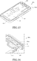
FIGS. 15 and 16 are views each illustrating the state in which a second injection-molded portion is formed in the housing in the manufacturing method of the electronic device according to another one of various embodiments of the present disclosure; and -
FIGS. 17 and 18 are views each illustrating the state in which a buffer member is completed in the manufacturing method of the electronic device according to another one of various embodiments of the present disclosure. - As the present disclosure allows for various changes and numerous embodiments, some exemplary embodiments will be described in detail with reference to the accompanying drawings. However, the embodiments do not limit the present disclosure to a specific implementation, but should be construed as including all modifications and replacements included in the scope of the present disclosure.
- Although ordinal terms such as "first" and "second" may be used to describe various elements, these elements are not limited by the terms. The terms are used merely for the purpose to distinguish an element from the other elements. For example, a first element could be termed a second element, and similarly, a second element could be also termed a first element without departing from the scope of the present disclosure. As used herein, the term "and/or" includes any and all combinations of one or more associated items.
- Further, the relative terms "a front surface", "a rear surface", "a top surface", "a bottom surface", and the like which are described with respect to the orientation in the drawings may be replaced by ordinal numbers such as first and second. In the ordinal numbers such as first and second, their order are determined in the mentioned order or arbitrarily and may not be arbitrarily changed if necessary.
- In the present specification, the terms are merely used to describe a specific embodiment, and are not intended to limit the present disclosure. As used herein, the singular forms are intended to include the plural forms as well, unless the context clearly indicates otherwise. In the description, it should be understood that the terms "include" or "have" indicate existence of a feature, a number, a step, an operation, a structural element, parts, or a combination thereof, and do not previously exclude the existences or probability of addition of one or more another features, numeral, steps, operations, structural elements, parts, or combinations thereof.
- Unless defined otherwise, all terms used herein, including technical and scientific terms, have the same meaning as commonly understood by those of skill in the art to which the present disclosure pertains. Such terms as those defined in a generally used dictionary are to be interpreted to have the meanings equal to the contextual meanings in the relevant field of art, and are not to be interpreted to have ideal or excessively formal meanings unless clearly defined in the present specification.
- In the present disclosure, an electronic device may be a random device with a touch panel, and the electronic device may be called a terminal, a portable terminal, a mobile terminal, a communication terminal, a portable communication terminal, a portable mobile terminal and display device or the like.
- For example, the electronic device may be a smartphone, a portable phone, a game player, a TV, a display unit, a heads-up display unit for a vehicle, a notebook computer, a laptop computer, a tablet Personal Computer (PC), a Personal Media Player (PMP), a Personal Digital Assistants (PDA), and the like. The electronic device may be implemented as a portable communication terminal which has a wireless communication function and a pocket size. Further, the electronic device may be a flexible device or a flexible display device.
- The electronic device may communicate with an external electronic device, such as a server or the like, or perform an operation through an interworking with the external electronic device. For example, the electronic device may transmit an image photographed by a camera and/or position information detected by a sensor unit to the server through a network. The network may be a mobile or cellular communication network, a Local Area Network (LAN), a Wireless Local Area Network (WLAN), a Wide Area Network (WAN), an Internet, a Small Area Network (SAN) or the like, but is not limited thereto.
-
FIG. 1 is a block diagram illustrating anelectronic device 20 according to an embodiment. Theelectronic device 20 may include, for example, the whole or a portion of theelectronic device 20 illustrated inFIG. 1 . Theelectronic device 20 may include at least one controller or processor (e.g., an application processor AP) 21, acommunication module 22, asubscriber identification module 22g, amemory 23, asensor module 24, aninput device 25, adisplay 26, aninterface 27, anaudio module 28, acamera module 29a, apower management module 29d, abattery 29e, anindicator 29b, and amotor 29c. Theprocessor 21 may drive, for example, an operating system or an application so as to control a plurality of hardware or software components connected thereto, and may also perform various data processing and arithmetic operations. Theprocessor 21 may be implemented by, for example, a system-on-chip (SoC). Theprocessor 21 may further include a graphic processing unit (GPU) and/or an image signal processor. Theprocessor 21 may include at least some components (e.g., acellular module 22a) among the components illustrated inFIG. 1 . Theprocessor 21 may load a command or data received from at least one of the other components (e.g., a non-volatile memory) in a volatile memory to process the command and data, and may store resultant data in a non-volatile memory. - The
communication module 22 may include, for example, thecellular module 22a, a Wi-Fi module 22b, aBluetooth module 22c, aGNSS module 22d, anNFC module 22e, and a radio frequency (RF)module 22f. Thecellular module 22a may provide, for example, a voice call, a video call, a message service, or an internet service through, for example, a communication network. Thecellular module 22a may perform discrimination and authentication of theelectronic device 20 within the communication network using the subscriber identification module (e.g., a SIM card) 22g. Thecellular module 22a may perform at least some of the functions that may be provided by theprocessor 21. Thecellular module 22a may include a communication processor (CP), and at least some (e.g., two or more) of thecellular module 22a, the Wi-Fi module 22b, theBluetooth module 22c, theGNSS module 22d, and theNFC module 22e may be incorporated in a single integrated chip (IC) or an IC package. TheRF module 22f may transmit/receive, for example, a communication signal (e.g., an RF signal). TheRF module 22f may include, for example, a transceiver, a power amp module (PAM), a frequency filter, a low noise amplifier (LNA), or an antenna. At least one of thecellular module 22a, the Wi-Fi module 22b, theBluetooth module 22c, theGNSS module 22d, and theNFC module 22e may transmit/receive an RF signal through one or more separate RF modules. Thesubscriber identification module 22g may include, for example, a card that includes a subscriber identification module and/or an embedded SIM, and may also include intrinsic identification information (e.g., integrated circuit card IDentifier (ICCID)) or subscriber information (e.g., international mobile subscriber identity (IMSI)). - The
memory 23 may include, for example, aninternal memory 23a or anexternal memory 23b. Theinternal memory 23a may include at least one of, for example, a volatile memory (e.g., a DRAM, an SRAM, or an SDRAM), a non-volatile memory (e.g., a One-Time Programmable ROM (OTPROM), a PROM, an EPROM, an EEPROM, a mask ROM, a flash ROM, a flash memory, a hard drive, and a Solid-State Drive (SSD). Theexternal memory 23b may further include a flash drive (e.g., a Compact Flash (CF), a Secure Digital (SD), a Micro Secure Digital (Micro-SD), a Mini Secure Digital (Mini-SD), an extreme Digital (xD), a Multi-Media Card (MMC), or a memory stick). Theexternal memory 23b may be functionally or physically connected to theelectronic device 20 through any of various interfaces. - For example, the
sensor module 24 may measure a physical quantity or may sense an operating status of theelectronic device 20, and may then convert the measured or sensed information into electric signals. Thesensor module 24 may include at least one of, for example, agesture sensor 24a, agyro sensor 24b, anatmospheric pressure sensor 24c, amagnetic sensor 24d, anacceleration sensor 24e, agrip sensor 24f, aproximity sensor 24g, acolor sensor 24h (e.g., RGB (Red, Green, Blue) sensor), a biometric sensor 24i, a temperature/humidity sensor 24j, anilluminance sensor 24k, and an Ultra-Violet (UV)sensor 241. Additionally, or alternatively, thesensor module 24 may include, for example, an E-nose sensor, an ElectroMyoGraphy (EMG) sensor, an ElectroEncephaloGram (EEG) sensor, an ElectroCardioGram (ECG) sensor, an Infra-Red (IR) sensor, an iris sensor, and/or a fingerprint sensor. Thesensor module 24 may further include a control circuit for controlling one or more sensors incorporated therein. In a certain embodiment, theelectronic device 20 may further include a processor configured to control thesensor module 24 as a portion of theprocessor 21 or separate from theprocessor 21 so as to control thesensor module 24 while theprocessor 21 is in a sleep state. - The
input device 25 may include, for example, atouch panel 25a, a (digital)pen sensor 25b, a key 25c, or anultrasonic input device 25d. As thetouch panel 25a, at least one of, for example, a capacitive-type touch panel, a resistive-type touch panel, an infrared-type touch panel, and an ultrasonic-type panel may be used. In addition, thetouch panel 25a may further include a control circuit. Thetouch panel 25a may further include a tactile layer so as to provide a tactile reaction to a user. The (digital)pen sensor 25b may be, for example, a portion of the touch panel, or may include a separate recognition sheet. The key 25c may include, for example, a physical button, an optical key, or a keypad. Theultrasonic input device 25d may sense, through a microphone (e.g., a microphone 28d), ultrasonic waves that are generated by an input tool so as to confirm data corresponding to the sensed ultrasonic waves. - The
display 26 may include apanel 26a, ahologram device 26b, aprojector 26c, and/or a control circuit for controlling these components. Thepanel 26a may be implemented to be, for example, flexible, transparent, or wearable. Thepanel 26a may be constituted with thetouch panel 25a and one or more modules. According to one embodiment, thepanel 26a may include a pressure sensor (or a force sensor) that is capable of measuring the intensity of pressure of a user's touch. The pressure sensor may be integrally implemented with thetouch panel 25a, or may be implemented by one or more sensors separately from thetouch panel 25a. Thehologram device 26b may show a stereoscopic image in the air using interference of light. Theprojector 26c may project light onto a screen so as to display an image. The screen may be located, for example, inside or outside theelectronic device 20. Theinterface 27 may include, for example, anHDMI 27a, aUSB 27b, anoptical interface 27c, or a D-subminiature (D-sub)interface 27d. Theinterface 27 may include, for example, a Mobile High-definition Link (MHL) interface, an SD card/Multi-Media Card (MMC) interface, or an Infrared Data Association (IrDA) standard interface. - The
audio module 28 may bi-directionally convert, for example, sound and electric signals. Theaudio module 28 may process sound information input or output through, for example, aspeaker 28a, areceiver 28b, an earphone 28c, or a microphone 28d. Thecamera module 29a is a device that is capable of taking, for example, a still image and a video image, and according to one embodiment, thecamera module 29a may include at least one image sensor (e.g., a front sensor or a rear sensor), a lens, an Image Signal Processor (ISP), or a flash (e.g., LED or xenon lamp). Thepower management module 29d may manage, for example, the electric power of theelectronic device 20. According to one embodiment, thepower management module 29d may include a Power Management Integrated Circuit (PMIC), a charger Integrated Circuit (IC), or a battery or fuel gauge. The PMIC may be configured as a wired and/or wireless charging type. The wireless charging type may include, for example, a magnetic resonance type, a magnetic induction type, or an electromagnetic wave type, and may further include an additional circuit for wireless charging (e.g., a coil loop, a resonance circuit, or a rectifier). The battery gauge may measure the remaining charge of thebattery 29e, and a voltage, a current, or a temperature while charging. Thebattery 29e may include, for example, a rechargeable battery and/or a solar battery. - The
indicator 29b may indicate a specific status of theelectronic device 20 or of a part thereof (e.g., the processor 21), such as a booting status, a message status, or a charged status. Themotor 29c may convert an electric signal into a mechanical vibration, and may generate, for example, a vibration or a haptic effect. Theelectronic device 20 may include, for example, a mobile TV support device (e.g., a GPU) that is capable of processing media data according to a standard of, for example, Digital Multimedia Broadcasting (DMB), Digital Video Broadcasting (DVB), or MediaFlo™. Each of the components described herein may be constituted with one or more components, and the names of the corresponding components may vary depending on the type of the electronic device. In various embodiments, an electronic device (e.g., the electronic device 20) may not include some of the components, or may include an additional component. Alternatively, some of the components may be combined with each other to be configured as one object, and to perform functions, which are the same as those of the corresponding components prior to the combination. -
FIG. 2 is a perspective view illustrating anelectronic device 100 according to various embodiments of the present disclosure.FIG. 3 is a front view illustrating theelectronic device 100 according to various embodiments of the present disclosure. - Referring to
FIGS. 2 to 3 , the electronic device 100 (e.g., theelectronic device 20 inFIG. 1 ) may include ahousing 101 and awindow glass 102 mounted on one face of thehousing 101. - According to various embodiments, the
housing 101 may accommodate, for example, the electronic components described with reference toFIG. 1 , and may at least partially include a metallic material portion. For example, a part or the entirety of thehousing 101 may be made of a metallic material. In some embodiments, some of the metallic material portions of thehousing 101 may be utilized as radiation conductors of the antenna device. For example, some of the metallic material portions of thehousing 101 may be connected to thecommunication module 22 ofFIG. 1 so as to transmit/receive wireless signals. - According to various embodiments, the
window glass 102 may be provided as a part or the entirety of a display device (e.g., thedisplay 26 inFIG. 1 ) of theelectronic device 100. For example, a display panel (e.g., thepanel 26a inFIG. 1 ) may be provided on the inner face of thewindow glass 102 so as to output an actual screen. In some embodiments, a touch panel (e.g., thetouch panel 25a inFIG. 1 ) may be disposed on thewindow glass 102, and a touch panel and a display panel may be combined so as to provide a touch screen function. For example, thewindow glass 102 may be an output device that at least partially outputs a screen, and may be utilized as an input device that generates an input signal corresponding to a touch input of a user. - In one embodiment, an input device such as a button or a touch key (e.g., the key 25c in
FIG. 1 ) may be provided on thelower side 102a of thewindow glass 102, and a sound module (e.g., thereceiver 28b ofFIG. 1 ) may be provided on theupper side 102b of thewindow glass 102. In some embodiments, the display panel may be provided to correspond to a region of thelower side 102a of thewindow glass 102, and may be combined with a touch panel disposed on thelower side 102a of thewindow glass 102 so as to replace a mechanically operated input device, such as a button. -
FIG. 4 is a cross-sectional view illustrating the electronic device according to various embodiments of the present disclosure in which a portion of the electronic device is cut away.FIG. 5 is a cross-sectional view illustrating the electronic device according to various embodiments of the present disclosure in which another portion of the electronic device is cut away. -
FIG. 4 is a cross-sectional view of theelectronic device 100 taken along, for example, line A-A' ofFIG. 3 , andFIG. 5 is a cross-sectional view of theelectronic device 100 taken along line B-B' ofFIG. 3 . - Further referring to
FIGS. 4 and 5 , theelectronic device 100 includes awindow glass 102 having inner and outer faces which are formed at least partially in a curved shape, for example, a three-dimensional shape. Adisplay panel 121 is coupled to theinner face 102a of thewindow glass 102, and thedisplay panel 121 at least partially has a curved shape corresponding to a shape of the inner face of thewindow glass 102. Anouter face 102b of the window glass provides a surface of a glass plate that covers at least a part of theelectronic device 100. The window glass 102 (and/or the display panel 121) may be bonded at least in part to thehousing 101 via an adhesive 119 (e.g., double-sided tape). The bonded portion of thehousing 101 may be formed as a curved surface corresponding to the curved portion of thewindow glass 102 and/or thedisplay panel 121. For example, the adhesive 119 may bond a portion of thewindow glass 102 and/or thedisplay panel 121 to a portion of thehousing 101. - According to various embodiments, the
electronic device 100 may include a buffer member (herein "buffer") 103. Thebuffer 103 may be formed of a synthetic, non-conductive resin material, e.g., polycarbonate, and may be formed along a portion of thehousing 101 as a molding member. Thebuffer 103 may be disposed adjacent to an edge area 102c of thewindow glass 102, and may be disposed between thewindow glass 102 and a metal portion of thehousing 101 comprising a metallic material, to reduce an impact or a load applied to thewindow glass 102 from transferring to thehousing 101. For example, thebuffer 103 is disposed adjacent to the edge area 102c of thewindow glass 102 while being disposed on at least the portion the metal portion of thehousing 101 that is includes a metallic material. Thebuffer 103 is disposed at least on the metallic material portion on one face of the housing, and is disposed adjacent to the edge area 102c of the window glass, i.e. glass cover, 102 such that the metallic material portion and the window glass portion of thehousing 101 are prevented from coming into direct contact with each other. - In some embodiments, the
housing 101 includes a metallic material portion and a non-metallic material portion (e.g., a synthetic resin material portion), in which a portion of thebuffer 103 may be formed on the metallic material portion and the remaining part of thebuffer 103 may be formed on the non-metallic material portion. As will be described with reference toFIG. 6 , thebuffer 103 may be formed in a closed curve on one face of thehousing 101, for example, on the face on which thewindow glass 102 is mounted. For example, thebuffer 103 may surround the region where thedisplay panel 121 is disposed and/or the region where the adhesive 119 is disposed. - In some embodiments, when an impact is applied to the
housing 101 due to being dropped or the like, the impact may be concentrated in a certain portion. For example, when a corner portion of thehousing 101 first collides with the floor, the impact may be concentrated in the corner portion. Thebuffer 103 may be formed only in a portion where the impact is concentrated, or may be formed thicker in the portion where the impact is concentrated while being formed to surround the portion where thedisplay panel 121 is disposed. - According to one embodiment, as illustrated in
FIG. 4 , thebuffer 103 may be partially exposed to the outside at the outside of the edge area 102c of thewindow glass 102. When thewindow glass 102 and thebuffer 103 are disposed as illustrated inFIG. 5 , thewindow glass 102 and thebuffer 103 can be seen from the outside through the edge area of thewindow glass 102. For example, thebuffer 103 may provide a decorative effect to the appearance of theelectronic device 100. - According to various embodiments, the
housing 101 may include a seating groove 131 (FIGs. 4 and 5 ) formed to correspond to at least a portion of the edge area 102c of thewindow glass 102. For example, theseating groove 131 may be formed in at least the metallic material portion of thehousing 101 in a region corresponding to the edge area 102c of thewindow glass 102. Thebuffer 103 may be formed at least partially in theseating groove 131. - According to various embodiments, in order to secure sufficient coupling force and/or bonding force between the housing 101 (and/or the metallic material portion of the housing 101) and the
buffer 103, a binding groove is formed in theseating groove 131. As shown inFIG. 5 , the binding groove includes, for example, a V-shapedgroove 133a formed in and/or recessed from the inner wall of theseating groove 131 and ascrew hole 133b formed in and/or recessed from the bottom of theseating groove 131. Thebuffer 103 may be formed of a synthetic resin, such as polycarbonate, and may be formed through an insert molding method in which the metallic material portion of thehousing 101 is placed in a mold and a molten resin is injected into the mold. - In the insert injection process, the binding force between the metallic material portion of the
housing 101 and thebuffer 103 may be weak. An electronic device (e.g., theelectronic device 100 ofFIG. 2 ) may include at least one binding groove formed in theseating groove 131, so that sufficient binding force and/or bonding force can be secured between the metallic material portion of thehousing 101 and thebuffer 103. In the process of forming thebuffer 103, a portion of thebuffer 103 may be formed to be engaged with the V-shapedgroove 133a and/or thescrew hole 133b. For example, a portion of thebuffer 103 is bound to the V-shapedgroove 133a and thescrew hole 133b (and/or the screw threads in thescrew hole 133b), so that thebuffer 103 dovetails with and is firmly coupled to the metallic material portion of thehousing 101. -
FIG. 6 is a front view illustrating thehousing 201 of the electronic device according to various embodiments of the present disclosure. - Referring to
FIG. 6 , thehousing 201 includes ametal portion 211 comprising a metallic material and a syntheticresin material portion 213, and may also include abuffer 203 inFIGS. 4 and 5 ) formed in an edge of one face thereof. Thehousing 201 may be formed of a metallic material, and may partially include a synthetic resin material portion, depending on the electronic components disposed within thehousing 201. For example, some electronic components (or modules), such as theproximity sensor 24g, theilluminance sensor 24k, thereceiver 28b, and themotor 29c inFIG. 1 , may be mounted in thehousing 201. When it is necessary to form an insulating structure between the electronic components mounted in thehousing 201 and other structures, the syntheticresin material portion 213 can be usefully utilized. The syntheticresin material portion 213 may be formed between a portion and another portion of themetallic material portion 211. For example, when a portion of themetallic material portion 211 is utilized as a radiation conductor of the antenna device, the syntheticresin material portion 213 may be interposed between a portion and another portion of themetallic material portion 211 so as to form an insulating structure. - In some embodiments, the synthetic
resin material portion 213 may be formed of polycarbonate or the like. When necessary to secure strength in a similar level to themetallic material portion 211, the syntheticresin material portion 213 may be formed of a synthetic resin to which glass fiber is added. The content of glass fiber in the syntheticresin material portion 213 or the like may be appropriately adjusted in consideration of the kind of the synthetic resin and the strength required for thehousing 201. For example, when the syntheticresin material portion 213 is formed of polycarbonate and themetallic material portion 211 is formed of aluminum, the syntheticresin material portion 213 may include glass fiber in an amount of about 40%. - According to various embodiments, as shown in
FIG. 6 , thebuffer 203 may be formed in a closed curve on one face of thehousing 201. For example, thebuffer 203 may extend along an edge of one face of thehousing 201, and may be disposed adjacent to an edge area of awindow glass 102 mounted on one face of thehousing 201. When thebuffer 203 forms a closed curve, the above-describedseating groove 131 may be formed in one face of thehousing 201 to extend (to be formed) along the edge of the face. Thebuffer 203 may be formed only in a portion where the impact is concentrated, or may be formed thicker in the portion where the impact is concentrated while being formed in a closed curve. -
FIG. 7 is a cross-sectional view illustrating anelectronic device 300 according to another one of various embodiments of the present disclosure. - Referring to
FIG. 7 , theelectronic device 300 may include awindow glass 302 in which at least a portion of an outer surface of thewindow glass 302 is formed in acurved face 329. The outer surface of thewindow glass 302 forms at least one portion of an outer surface of theelectronic device 300. For example, thewindow glass 302 may have an edge area formed in a curved shape, and may be coupled to thehousing 301 with thedisplay panel 321 interposed adjacent to thewindow glass 302. Thehousing 301 includes a metal portion generally formed of a metallic material, and includes abuffer 303 disposed adjacent to the edge area of thewindow glass 302. Thebuffer 303 includes agroove 333 formed to secure within a similarly shaped recess of thehousing 301. For example, thebuffer 303 may be formed as a portion of thehousing 301, and may be disposed at least between the edge area of thewindow glass 302 and the metal portion of thehousing 301. To affix thewindow glass 302 and/or thedisplay panel 321 on thehousing 301, anadhesive member 319 may be used to bond a portion of thewindow glass 302 onto thehousing 301. -
FIG. 8 is a flowchart illustrating a manufacturing method of the electronic device (400) according to another one of various embodiments of the present disclosure.FIG. 9 is a flowchart illustrating an operation of preparing a housing (401) in the manufacturing method of the electronic device according to another one of various embodiments of the present disclosure.FIG. 10 is a flowchart illustrating an operation of forming a buffer member (402) in the manufacturing method of the electronic device according to another one of various embodiments of the present disclosure. -
FIGS. 11 and 12 are views each illustrating the state in which a first injection-molded portion is formed in the housing (501a) in the manufacturing method of the electronic device according to another one of various embodiments of the present disclosure.FIGS. 13 and 14 are views each illustrating the state in which the housing is processed in which the first injection-molded portion is formed (501b) in the manufacturing method of the electronic device according to another one of various embodiments of the present disclosure.FIGS. 15 and 16 are views each illustrating the state in which a second injection-molded portion is formed in the housing (501c) in the manufacturing method of the electronic device according to another one of various embodiments of the present disclosure.FIGS. 17 and 18 are views each illustrating the state in which a buffer member is completed (501d) in the manufacturing method of the electronic device according to another one of various embodiments of the present disclosure. - Referring to
FIG. 8 , a manufacturing method of anelectronic device 100 includes, instep 401, preparing a housing, which is at least partially formed of a metallic material. In step 402 abuffer 203 is formed on one face of the prepared housing, and in step 404 awindow glass 102 is mounted on one face of the housing, which is formed with the buffer. When the window glass is mounted on the housing, a buffer may be disposed at least between the metallic material portion of the housing and the edge area of the window glass. For example, the buffer may be disposed adjacent to the edge area of the window glass while being disposed at least in the metal portion of the housing. - Further referring to
FIG. 9 , the operation of preparing the housing includes forming, instep 411, the metallic material portion and processing a seating groove instep 415. When necessary to partially isolate the metallic material portion of the housing and/or a portion between the housing to be formed and an electronic component, the operation of preparing the housing further includesstep 413 that is performed afterstep 411 of forming a first injection-molded portion before processing the seating groove ofstep 415. - The
step 411 of forming the metallic material portion is an operation for forming the metallic material portion of the housing to be manufactured, and may be performed through a die-casting process. The metallic material portion of the housing to be manufactured may be formed of, for example, aluminum. In some embodiments, the forming of the metallic material portion may include cutting a flat aluminum plate having a predetermined thickness. - The
step 413 of forming the first injection-molded portion may be performed when it is necessary to form an insulating portion in the housing to be manufactured. Thestep 413 of forming the first injection-molded portion may be performed through an insert injection process in which a molten resin is injected while the formed metallic material portion is disposed in the mold. The molten resin injected into the mold in thestep 413 of forming the first injection-molded portion may be generally polycarbonate, and may include glass fiber in an amount of about 40%. Ahousing 501a (hereinafter, "primarily moldedhousing 501a"), which is formed with a first injection-molded portion, is illustrated inFIGS. 11 and 12 . As shown inFIGS. 11 and 12 , a first injection-moldedportion 513 may be formed to partially enclose an area between a portion of ametallic material portion 511 and/or another portion thereof. - The processing of the seating groove in
step 415 ofFIG. 9 is an operation for processing the primarily moldedhousing 501a, and may remove, for example, an unnecessary portion of the first injection-molded portion 513 (e.g., a molded portion corresponding to a gate or the like for injecting a molten resin), or may form a seating groove in one face of the primarily moldedhousing 501a. The operation for forming the seating groove may be performed, for example, through a cutting process using a computer controlled lathe or the like, and a seating groove may be formed in an edge area of one face of the primarily moldedhousing 501a. Ahousing 501b (hereinafter, "primarily processedhousing 501b"), which is formed with a seating groove, is illustrated inFIGS. 13 and 14 . Referring toFIGS. 13 and 14 , aseating groove 531 is formed along the edge area on one face of the primarily processedhousing 501b to form, for example, a closed curve. The operation of processing theseating groove 531 includes removing a portion of the first injection-moldedportion 513. A binding groove (e.g., the V-shapedgroove 133a or thescrew hole 133b inFIG. 5 ) may be formed in the inner wall and/or the bottom of theseating groove 531 when theseating groove 531 is formed instep 415 ofFIG. 9 . - Further referring to
FIGs. 8 and10 , forming the buffer instep 402 may include forming the second injection-molded portion ofstep 421 ofFIG. 10 and theprocessing step 423 of the second injection-molded portion. Forming the second injection-molded portion may form the second injection-molded portion by injecting a molten resin (e.g., polycarbonate) in a state in which the primarily processedhousing 501b (FIG. 14 ) is seated in the mold. For example, the second injection-molded portion may be formed in theseating groove 531 in the primarily processedhousing 501b. Ahousing 501c (hereinafter, "secondarily moldedhousing 501c"), which is formed with a secondarily injection-molded portion, is illustrated inFIGS. 15 and 16 . Referring toFIGS. 15 and 16 , when the molten resin is injected into the mold, a second injection-moldedportion 503a is filled and hardened in theseating groove 531. The molten resin filled in theseating groove 531 may include polycarbonate and may not contain glass fiber, so that the resin filled in theseating groove 531 may have a lower strength (e.g., hardness) than the first injection-moldedportion 513. According to some embodiments, in the operation of forming the second injection-moldedportion 503a, some of the molten resin may be injected into the above-described binding groove (e.g., the V-shapedgroove 133a and thescrew hole 133b inFIG. 5 ). For example, the second injection-moldedpart 503a may be partially engaged with the above-described binding groove while being molded. - The
processing operation 423 partially processes and removes the second injection-moldedportion 503a so that the buffer can be completed in a shape corresponding to the edge area of thewindow glass 102. The buffer may be formed, for example, by partially removing the second injection-moldedportion 503a through a cutting process using a computer numerically-controlled lathe. For example, the buffer may be a portion of the second injection-moldedportion 503a. Ahousing 501d (hereinafter, "secondarily processedhousing 501d") in which the buffer is completed is illustrated inFIGS. 17 and 18 . Referring toFIGS. 17 and 18 , thebuffer 503b may be formed on themetallic material portion 511 of the secondarily processedhousing 501d and may be partially formed on the first injection-molded portion 513 (e.g., the syntheticresin material portion 213 inFIG. 6 ). Thebuffer 503b may be formed along the edge area of one face of the secondarily processedhousing 501d, and may have a closed curve shape. - According to one embodiment, the
metallic material portion 511 of the secondarily moldedhousing 501c is also partially removed in the processing operation ofstep 423 ofFIG. 10 such that thehousing 201 can be completed. For example, the flat outer wall S1 of the secondarily moldedhousing 501c illustrated inFIG. 16 has a curved shape like the outer wall S2 of the secondarily processedhousing 501d illustrated inFIG. 18 . - As described above, the processing operation of
step 423 ofFIG. 10 may complete thebuffer 503b, and complete the shape of the housing 201 (FIG. 6 ). The process of completing thebuffer 503b and the process of partially removing the metal portion of the secondarily moldedhousing 501c are performed in separate operations. For example, the operation of processing thebuffer 503b made of a synthetic resin material and themetallic material portion 511 of the secondarily moldedhousing 501c may be performed independently. - Referring to
FIG. 8 , the operation for mounting the window glass instep 404 couples a glass cover, 102 to one face of the secondarily processedhousing 501d, in which the window glass may be coupled to the secondarily processedhousing 501d through an adhesive such as double-sided tape. - According to various embodiments, the manufacturing method further includes a finishing process (step 403 of
FIG. 8 ) performed on the secondarily processedhousing 501d ofFIG. 18 . The finishing process of step 403 may include, for example, a surface treatment for providing various tactile sensations on the face which is touched by the user, a painting or coloring treatment and a discoloration/corrosion prevention treatment for a portion exposed to the external environment, etc. When the manufacturing method includes the operation for performing the finishing process of step 403, the window glass will be coupled to the housing subjected to the finishing process. - As described above, according to various embodiments of the present disclosure, an electronic device may include: a housing at least partially including a metallic material portion; a window glass mounted on one surface of the housing; and a buffer member disposed at least on the metallic material portion on one face of the housing, and disposed adjacent to an edge of the window glass.
- According to various embodiments, the buffer member may be formed on one face of the housing to form a closed curve.
- According to various embodiments, the buffer member may be formed of a synthetic resin including polycarbonate.
- According to various embodiments, the housing may include a seating groove formed in one face to correspond to at least a portion of an edge of the window glass, and at least a portion of the buffer member may be accommodated in the seating groove.
- According to various embodiments, the housing may further include a binding groove formed in the seating groove, and a portion of the buffer member may be bound with the binding groove.
- According to various embodiments, the binding groove may include a screw hole.
- According to various embodiments, the buffer member may be formed on one face of the housing to form a closed curve.
- According to various embodiments, a portion of the buffer member may be exposed outside the edge of the window glass.
- According to various embodiments, at least outer face of the edge of the window glass may be formed to form a curved face.
- According to various embodiments, the inner face and outer face of the edge of the window glass may be formed to form a curved face.
- According to various embodiments, the above-described electronic device may further include a display panel coupled to an inner face of the window glass, and an adhesive member that bonds a portion of the display panel to one face of the housing.
- The buffer member may be formed in a closed curve that surrounds a region where at least the adhesive member is bonded.
- According to various embodiments of the present disclosure, a method of manufacturing the above-described electronic device may include preparing a housing, which is at least partially made of a metallic material, forming a buffer member on one face of the prepared housing, and mounting a window glass on the one face of the housing in which the buffer member is formed.
- The buffer member may be disposed at least on the metallic material portion on the one face of the housing, and may be disposed adjacent to an edge of the window glass.
- According to various embodiments, the preparing the housing may include forming the metallic material portion and processing a seating groove in which the buffer member is to be disposed, by processing at least the metallic material portion.
- According to various embodiments, the preparing the housing may include forming a first injection-molded portion in the state in which the formed metallic material portion is seated in a mold prior to processing the seating groove.
- According to various embodiments, the processing the seating groove may include forming a binding groove in the formed seating groove.
- According to various embodiments, a portion of the buffer member may be configured to be engaged in the binding groove.
- According to various embodiments, the forming the buffer member may include forming a secondarily injection-molded portion in the state in which the prepared housing is seated in the mold and completing the buffer member by processing the secondarily injection-molded portion to correspond to an edge portion of the window glass.
- According to various embodiments, the method may further include processing the housing in which the buffer member is formed prior to mounting the window glass.
- In the processing the housing in which the buffer member is formed, the shape of the buffer member may be completed to correspond to the edge portion of the window glass.
- According to various embodiments, the method may further include finishing the processed housing after the operation of processing the housing in which the buffer member is formed.
- According to various embodiments, the finishing operation may include coloring the surface of the processed housing.
- In the foregoing detailed description, specific embodiments of the present disclosure have been described. However, it will be evident to a person ordinarily skilled in the art that various modifications may be made without departing from the scope of the present disclosure.
Claims (12)
- A portable communication device (100, 200, 300, 400) comprising:a housing (101, 201, 301, 401) including a metal housing member (211) at least partially forming an outer side surface of the portable communication device, a seating groove (131, 415, 531) formed in the metal housing member, the metal housing member including a first metal portion and a second metal portion;a resin member including a first portion (103, 203, 303) formed in the seating groove of the metal housing member and a second portion (213) formed between the first metal portion and the second metal portion; anda window glass (102) forming at least a part of an outer surface of the portable communication device,wherein the first portion (103, 203, 303) of the resin member is partially exposed to an outside of the portable communication device between the metal housing member and the window glass and the second portion (213) of the resin member is partially exposed to the outside of the portable communication device between the first metal portion and the second metal portion, andwherein at least one of the first metal portion and the second metal portion is configured to be utilized as radiation conductors.
- The portable communication device (100, 200, 300, 400) of claim 1, wherein the second portion (213) of the resin member formed between the first metal portion and the second metal portion is configured to form an insulating structure between the first metal portion and the second metal portion.
- The portable communication device (100, 200, 300, 400) of claim 1, wherein the second portion of the resin member extends from the first portion of the resin member.
- The portable communication device (100, 200, 300, 400) of claim 1, wherein the first portion of the resin member, exposed to the outside of the electronic device, is formed in a closed curve on one face of the housing.
- The portable communication device (100, 200, 300, 400) of anyone of the preceding claims, wherein the resin member is formed by insert molding in which a molten resin is injected into the seating groove such that the first portion of the resin member is configured to correspond to a curvature of an outer surface in an edge region of the window glass and a curvature of an outer surface of the metal housing member.
- The portable communication device (100, 200, 300, 400) of anyone of the preceding claims, further comprising a binding groove (133a, 133b) formed together with the seating groove on the metal housing member,
wherein the resin member is formed through an insert molding in which a molten resin is injected into both the seating groove and the binding groove. - The portable communication device (100, 200, 300, 400) of claim 6, wherein the resin member is formed by insert molding in which a molten resin is injected into the binding groove such that the portion of the first portion of the resin member is fixedly engaged with the binding groove.
- The portable communication device (100, 200, 300, 400) of claim 6, wherein the binding groove includes one of a V-shaped groove (133a) and a screw hole.
- The portable communication device (100, 200, 300, 400) of claim 6, wherein the binding groove is formed from an inner wall and/or a bottom of the seating groove.
- The portable communication device (100, 200, 300, 400) of claim 1, wherein an edge area of the window glass bonded to the housing is curved away from a planar area of the window glass.
- The portable communication device (100, 200, 300, 400) of claim 10, wherein, at least when the housing is deformed by an external impact, the first portion of the resin member is configured to prevent the metal housing member from coming into contact directly with at least one portion of the edge area of the window glass.
- The portable communication device (100, 200, 300, 400) of claim 1, further comprising:
a communication module electrically connected at least one of the first metal portion and a second metal portion, and configured to transmit/receive wireless signals using the at least one of the first metal portion and a second metal portion.
Applications Claiming Priority (4)
| Application Number | Priority Date | Filing Date | Title |
|---|---|---|---|
| KR1020160130918A KR102279735B1 (en) | 2016-10-10 | 2016-10-10 | Electronic device and manufacturing method of the same |
| EP17859833.0A EP3407578B1 (en) | 2016-10-10 | 2017-09-22 | Electronic device and manufacturing method therefor |
| EP20169200.1A EP3697066B1 (en) | 2016-10-10 | 2017-09-22 | Electronic device and manufacturing method thereof |
| PCT/KR2017/010491 WO2018070691A1 (en) | 2016-10-10 | 2017-09-22 | Electronic device and manufacturing method therefor |
Related Parent Applications (2)
| Application Number | Title | Priority Date | Filing Date |
|---|---|---|---|
| EP17859833.0A Division EP3407578B1 (en) | 2016-10-10 | 2017-09-22 | Electronic device and manufacturing method therefor |
| EP20169200.1A Division EP3697066B1 (en) | 2016-10-10 | 2017-09-22 | Electronic device and manufacturing method thereof |
Publications (3)
| Publication Number | Publication Date |
|---|---|
| EP4009618A1 true EP4009618A1 (en) | 2022-06-08 |
| EP4009618C0 EP4009618C0 (en) | 2023-06-07 |
| EP4009618B1 EP4009618B1 (en) | 2023-06-07 |
Family
ID=61906155
Family Applications (3)
| Application Number | Title | Priority Date | Filing Date |
|---|---|---|---|
| EP22153239.3A Active EP4009618B1 (en) | 2016-10-10 | 2017-09-22 | Electronic device |
| EP20169200.1A Active EP3697066B1 (en) | 2016-10-10 | 2017-09-22 | Electronic device and manufacturing method thereof |
| EP17859833.0A Active EP3407578B1 (en) | 2016-10-10 | 2017-09-22 | Electronic device and manufacturing method therefor |
Family Applications After (2)
| Application Number | Title | Priority Date | Filing Date |
|---|---|---|---|
| EP20169200.1A Active EP3697066B1 (en) | 2016-10-10 | 2017-09-22 | Electronic device and manufacturing method thereof |
| EP17859833.0A Active EP3407578B1 (en) | 2016-10-10 | 2017-09-22 | Electronic device and manufacturing method therefor |
Country Status (8)
| Country | Link |
|---|---|
| US (3) | US10778819B2 (en) |
| EP (3) | EP4009618B1 (en) |
| KR (3) | KR102279735B1 (en) |
| CN (2) | CN113225420B (en) |
| ES (2) | ES2805454T3 (en) |
| HU (1) | HUE062771T2 (en) |
| PL (1) | PL4009618T3 (en) |
| WO (1) | WO2018070691A1 (en) |
Families Citing this family (20)
| Publication number | Priority date | Publication date | Assignee | Title |
|---|---|---|---|---|
| CN106102389B (en) * | 2016-08-16 | 2018-05-29 | 广东欧珀移动通信有限公司 | A kind of processing method of housing, housing and mobile terminal |
| KR102279735B1 (en) * | 2016-10-10 | 2021-07-20 | 삼성전자주식회사 | Electronic device and manufacturing method of the same |
| CN110149434B (en) * | 2018-02-13 | 2021-09-14 | 深圳富泰宏精密工业有限公司 | Electronic device and preparation method thereof |
| WO2019211941A1 (en) * | 2018-05-01 | 2019-11-07 | 株式会社村田製作所 | Electronic device and fingerprint authentication device mounted therewith |
| KR102040318B1 (en) * | 2018-08-08 | 2019-11-04 | 삼성전자주식회사 | Electronic device and housing structure |
| KR102509085B1 (en) | 2018-08-08 | 2023-03-13 | 삼성전자주식회사 | An electronic device comprising a metal material |
| KR102551690B1 (en) | 2018-12-06 | 2023-07-05 | 삼성전자주식회사 | Electronic device with bonding structure |
| CN109862723B (en) * | 2018-12-29 | 2021-08-06 | 维沃移动通信有限公司 | Preparation method of shell, shell and terminal equipment |
| KR102632789B1 (en) | 2019-04-22 | 2024-02-02 | 삼성전자주식회사 | Electronic device having display |
| KR20200127741A (en) * | 2019-05-03 | 2020-11-11 | 삼성전자주식회사 | Electronic device including display |
| USD947850S1 (en) * | 2019-11-22 | 2022-04-05 | Apple Inc. | Housing module for an electronic device |
| USD957402S1 (en) * | 2019-11-22 | 2022-07-12 | Apple Inc. | Housing module for an electronic device |
| USD947849S1 (en) * | 2019-11-22 | 2022-04-05 | Apple Inc. | Housing module for an electronic device |
| USD947851S1 (en) * | 2019-11-22 | 2022-04-05 | Apple Inc. | Housing module for an electronic device |
| US11838432B2 (en) * | 2019-12-03 | 2023-12-05 | Apple Inc. | Handheld electronic device |
| EP4089503A4 (en) * | 2020-02-10 | 2023-06-28 | Samsung Electronics Co., Ltd. | Electronic device including display |
| WO2022065806A1 (en) * | 2020-09-22 | 2022-03-31 | 삼성전자 주식회사 | Housing having recess structure and electronic device including same |
| CN112689040A (en) * | 2020-12-30 | 2021-04-20 | Oppo(重庆)智能科技有限公司 | Electronic device |
| WO2023068544A1 (en) * | 2021-10-19 | 2023-04-27 | 삼성전자 주식회사 | Electronic device comprising metal member |
| WO2024019580A1 (en) * | 2022-07-22 | 2024-01-25 | 삼성전자주식회사 | Buffer frame module and electronic device comprising same |
Citations (4)
| Publication number | Priority date | Publication date | Assignee | Title |
|---|---|---|---|---|
| CN103974570A (en) * | 2013-01-25 | 2014-08-06 | 云辉科技股份有限公司 | Composite molded window protection structure and electronic device composed of composite molded window protection structure |
| US20150155614A1 (en) * | 2013-12-03 | 2015-06-04 | Lg Electronics Inc. | Mobile Terminal |
| EP2993872A1 (en) * | 2014-09-02 | 2016-03-09 | Samsung Electronics Co., Ltd | Curved display and electronic device including the same |
| EP3054655A1 (en) * | 2015-02-06 | 2016-08-10 | Samsung Electronics Co., Ltd. | Electronic device including display with bent area |
Family Cites Families (37)
| Publication number | Priority date | Publication date | Assignee | Title |
|---|---|---|---|---|
| JPH11122330A (en) * | 1997-10-09 | 1999-04-30 | Kokusai Electric Co Ltd | Liquid crystal display section protection mechanism for portable communication equipment |
| KR20070013127A (en) * | 2005-07-25 | 2007-01-30 | 주식회사 팬택앤큐리텔 | Mobile communication terminal with cushion for display |
| KR101480454B1 (en) * | 2008-04-07 | 2015-01-09 | 엘지전자 주식회사 | Portable terminal |
| CN101998780B (en) * | 2009-08-24 | 2013-10-30 | 宏达国际电子股份有限公司 | Case assembly of handheld electronic device and manufacturing method thereof |
| US8385060B2 (en) * | 2009-08-31 | 2013-02-26 | Apple Inc. | Handheld computing device |
| CN102001154A (en) * | 2009-09-03 | 2011-04-06 | 鸿富锦精密工业(深圳)有限公司 | Manufacturing method of shell |
| CN102006747B (en) * | 2009-09-03 | 2015-07-29 | 鸿富锦精密工业(深圳)有限公司 | Housing |
| CN102006739A (en) * | 2009-09-03 | 2011-04-06 | 鸿富锦精密工业(深圳)有限公司 | Shell |
| US8797721B2 (en) * | 2010-02-02 | 2014-08-05 | Apple Inc. | Portable electronic device housing with outer glass surfaces |
| WO2012002197A1 (en) * | 2010-07-02 | 2012-01-05 | Semiconductor Energy Laboratory Co., Ltd. | Liquid crystal display device |
| KR20120029960A (en) * | 2010-09-17 | 2012-03-27 | 공석태 | Touch screen panel |
| JP5605176B2 (en) * | 2010-11-10 | 2014-10-15 | 旭硝子株式会社 | Cover glass for flat panel display and manufacturing method thereof |
| TWI452902B (en) * | 2011-01-05 | 2014-09-11 | Inventec Corp | Display module |
| CN102869211A (en) * | 2011-07-08 | 2013-01-09 | 深圳富泰宏精密工业有限公司 | Casing and manufacturing method thereof |
| US9001002B2 (en) * | 2011-09-30 | 2015-04-07 | Apple Inc. | Portable electronic device housing having insert molding around antenna |
| JP5943003B2 (en) * | 2011-12-14 | 2016-06-29 | コニカミノルタ株式会社 | Cover glass and manufacturing method thereof |
| KR20130081513A (en) * | 2012-01-09 | 2013-07-17 | 엘지전자 주식회사 | Mobile terminal |
| KR20130085218A (en) * | 2012-01-19 | 2013-07-29 | 엘지전자 주식회사 | Mobile terminal |
| US9047044B2 (en) * | 2012-10-19 | 2015-06-02 | Apple Inc. | Trimless glass enclosure interface |
| CN103078974B (en) * | 2013-01-07 | 2015-11-25 | 华为终端有限公司 | Hand-held electronic product |
| US9623628B2 (en) * | 2013-01-10 | 2017-04-18 | Apple Inc. | Sapphire component with residual compressive stress |
| JP6169881B2 (en) * | 2013-04-26 | 2017-07-26 | 京セラ株式会社 | Electronics |
| KR101399835B1 (en) * | 2013-07-09 | 2014-05-27 | 박상인 | Method of manufacturing case for mobile device and case for mobile device manufactured by the same method |
| US10434741B2 (en) * | 2013-07-18 | 2019-10-08 | Daicel Polymer Ltd. | Composite molded article |
| CN203445915U (en) * | 2013-08-09 | 2014-02-19 | 上海闻泰电子科技有限公司 | Novel mobile phone |
| KR102489694B1 (en) * | 2013-08-30 | 2023-01-19 | 가부시키가이샤 한도오따이 에네루기 켄큐쇼 | Display device |
| CN203535596U (en) * | 2013-09-24 | 2014-04-09 | 东莞宇龙通信科技有限公司 | Touch terminal and front shell thereof |
| KR102119660B1 (en) * | 2013-10-17 | 2020-06-08 | 엘지전자 주식회사 | Mobile terminal |
| JP6314709B2 (en) * | 2014-07-10 | 2018-04-25 | 富士通株式会社 | Electronic device and its assembly method |
| KR102208686B1 (en) * | 2014-08-11 | 2021-01-28 | 삼성전자주식회사 | Electronic device and fabrication method of the same |
| KR101695709B1 (en) * | 2014-08-12 | 2017-01-12 | 삼성전자주식회사 | Housing, manufacturing method thereof, and electronic device having it |
| US10509439B2 (en) * | 2014-09-02 | 2019-12-17 | Samsung Electronics Co., Ltd. | Curved display, display case, and electronic device including the same |
| KR102296846B1 (en) * | 2015-02-06 | 2021-09-01 | 삼성전자주식회사 | Key button assembly and electronic device having it |
| US9750322B2 (en) * | 2015-03-08 | 2017-09-05 | Apple Inc. | Co-molded ceramic and polymer structure |
| KR102279735B1 (en) * | 2016-10-10 | 2021-07-20 | 삼성전자주식회사 | Electronic device and manufacturing method of the same |
| KR102592054B1 (en) * | 2016-12-23 | 2023-10-23 | 삼성전자주식회사 | electronic device including glass housing |
| US10705570B2 (en) * | 2018-08-30 | 2020-07-07 | Apple Inc. | Electronic device housing with integrated antenna |
-
2016
- 2016-10-10 KR KR1020160130918A patent/KR102279735B1/en active IP Right Grant
-
2017
- 2017-09-22 EP EP22153239.3A patent/EP4009618B1/en active Active
- 2017-09-22 CN CN202110389281.4A patent/CN113225420B/en active Active
- 2017-09-22 PL PL22153239.3T patent/PL4009618T3/en unknown
- 2017-09-22 HU HUE22153239A patent/HUE062771T2/en unknown
- 2017-09-22 ES ES17859833T patent/ES2805454T3/en active Active
- 2017-09-22 EP EP20169200.1A patent/EP3697066B1/en active Active
- 2017-09-22 EP EP17859833.0A patent/EP3407578B1/en active Active
- 2017-09-22 ES ES22153239T patent/ES2947210T3/en active Active
- 2017-09-22 CN CN201780012367.7A patent/CN108702405B/en active Active
- 2017-09-22 WO PCT/KR2017/010491 patent/WO2018070691A1/en active Application Filing
-
2018
- 2018-08-07 US US16/057,048 patent/US10778819B2/en active Active
-
2020
- 2020-09-14 US US17/020,291 patent/US11082545B2/en active Active
-
2021
- 2021-06-29 US US17/362,368 patent/US20210329107A1/en active Pending
- 2021-07-14 KR KR1020210092410A patent/KR102397895B1/en active IP Right Grant
-
2022
- 2022-05-10 KR KR1020220057236A patent/KR102589601B1/en active IP Right Grant
Patent Citations (4)
| Publication number | Priority date | Publication date | Assignee | Title |
|---|---|---|---|---|
| CN103974570A (en) * | 2013-01-25 | 2014-08-06 | 云辉科技股份有限公司 | Composite molded window protection structure and electronic device composed of composite molded window protection structure |
| US20150155614A1 (en) * | 2013-12-03 | 2015-06-04 | Lg Electronics Inc. | Mobile Terminal |
| EP2993872A1 (en) * | 2014-09-02 | 2016-03-09 | Samsung Electronics Co., Ltd | Curved display and electronic device including the same |
| EP3054655A1 (en) * | 2015-02-06 | 2016-08-10 | Samsung Electronics Co., Ltd. | Electronic device including display with bent area |
Also Published As
| Publication number | Publication date |
|---|---|
| CN108702405A (en) | 2018-10-23 |
| HUE062771T2 (en) | 2023-12-28 |
| US20180343332A1 (en) | 2018-11-29 |
| KR102397895B1 (en) | 2022-05-16 |
| CN113225420A (en) | 2021-08-06 |
| KR20220066234A (en) | 2022-05-24 |
| US10778819B2 (en) | 2020-09-15 |
| PL4009618T3 (en) | 2023-11-06 |
| US11082545B2 (en) | 2021-08-03 |
| US20200412851A1 (en) | 2020-12-31 |
| EP3407578A1 (en) | 2018-11-28 |
| CN108702405B (en) | 2021-12-07 |
| EP3697066B1 (en) | 2022-02-23 |
| KR20210092166A (en) | 2021-07-23 |
| EP4009618C0 (en) | 2023-06-07 |
| EP3407578B1 (en) | 2020-05-13 |
| KR102589601B1 (en) | 2023-10-17 |
| ES2947210T3 (en) | 2023-08-03 |
| EP3407578A4 (en) | 2019-04-03 |
| EP4009618B1 (en) | 2023-06-07 |
| KR102279735B1 (en) | 2021-07-20 |
| WO2018070691A1 (en) | 2018-04-19 |
| KR20180039522A (en) | 2018-04-18 |
| EP3697066A1 (en) | 2020-08-19 |
| US20210329107A1 (en) | 2021-10-21 |
| ES2805454T3 (en) | 2021-02-12 |
| CN113225420B (en) | 2023-11-03 |
Similar Documents
| Publication | Publication Date | Title |
|---|---|---|
| EP4009618B1 (en) | Electronic device | |
| US11914424B2 (en) | Display device and electronic device having same | |
| US10431887B2 (en) | Electronic device with electromagnetic shielding member | |
| CN108475847B (en) | Antenna device and electronic device including the same | |
| EP3375174B1 (en) | Electronic device having unibody housing and method of manufacturing the same | |
| US9735825B2 (en) | Electronic device and method for controlling display on basis of information of accessory device and accessory device related thereto | |
| CN105676951A (en) | Electronic equipment with tray for accommodating cards | |
| CN105813554A (en) | Sensor device and electronic device having the same | |
| US20160374219A1 (en) | Electronic device | |
| EP3180867B1 (en) | Electronic device, method for controlling the electronic device, recording medium, and ear-jack terminal cap interworking with the electronic device |
Legal Events
| Date | Code | Title | Description |
|---|---|---|---|
| PUAI | Public reference made under article 153(3) epc to a published international application that has entered the european phase |
Free format text: ORIGINAL CODE: 0009012 |
|
| STAA | Information on the status of an ep patent application or granted ep patent |
Free format text: STATUS: THE APPLICATION HAS BEEN PUBLISHED |
|
| AC | Divisional application: reference to earlier application |
Ref document number: 3407578 Country of ref document: EP Kind code of ref document: P Ref document number: 3697066 Country of ref document: EP Kind code of ref document: P |
|
| AK | Designated contracting states |
Kind code of ref document: A1 Designated state(s): AL AT BE BG CH CY CZ DE DK EE ES FI FR GB GR HR HU IE IS IT LI LT LU LV MC MK MT NL NO PL PT RO RS SE SI SK SM TR |
|
| STAA | Information on the status of an ep patent application or granted ep patent |
Free format text: STATUS: REQUEST FOR EXAMINATION WAS MADE |
|
| 17P | Request for examination filed |
Effective date: 20220713 |
|
| RBV | Designated contracting states (corrected) |
Designated state(s): AL AT BE BG CH CY CZ DE DK EE ES FI FR GB GR HR HU IE IS IT LI LT LU LV MC MK MT NL NO PL PT RO RS SE SI SK SM TR |
|
| GRAP | Despatch of communication of intention to grant a patent |
Free format text: ORIGINAL CODE: EPIDOSNIGR1 |
|
| STAA | Information on the status of an ep patent application or granted ep patent |
Free format text: STATUS: GRANT OF PATENT IS INTENDED |
|
| INTG | Intention to grant announced |
Effective date: 20221129 |
|
| GRAS | Grant fee paid |
Free format text: ORIGINAL CODE: EPIDOSNIGR3 |
|
| GRAA | (expected) grant |
Free format text: ORIGINAL CODE: 0009210 |
|
| STAA | Information on the status of an ep patent application or granted ep patent |
Free format text: STATUS: THE PATENT HAS BEEN GRANTED |
|
| AC | Divisional application: reference to earlier application |
Ref document number: 3407578 Country of ref document: EP Kind code of ref document: P Ref document number: 3697066 Country of ref document: EP Kind code of ref document: P |
|
| AK | Designated contracting states |
Kind code of ref document: B1 Designated state(s): AL AT BE BG CH CY CZ DE DK EE ES FI FR GB GR HR HU IE IS IT LI LT LU LV MC MK MT NL NO PL PT RO RS SE SI SK SM TR |
|
| REG | Reference to a national code |
Ref country code: GB Ref legal event code: FG4D |
|
| REG | Reference to a national code |
Ref country code: CH Ref legal event code: EP Ref country code: AT Ref legal event code: REF Ref document number: 1578184 Country of ref document: AT Kind code of ref document: T Effective date: 20230615 |
|
| REG | Reference to a national code |
Ref country code: DE Ref legal event code: R096 Ref document number: 602017070130 Country of ref document: DE |
|
| REG | Reference to a national code |
Ref country code: ES Ref legal event code: FG2A Ref document number: 2947210 Country of ref document: ES Kind code of ref document: T3 Effective date: 20230803 |
|
| U01 | Request for unitary effect filed |
Effective date: 20230703 |
|
| U07 | Unitary effect registered |
Designated state(s): AT BE BG DE DK EE FI FR IT LT LU LV MT NL PT SE SI Effective date: 20230710 |
|
| U20 | Renewal fee paid [unitary effect] |
Year of fee payment: 7 Effective date: 20230809 |
|
| REG | Reference to a national code |
Ref country code: LT Ref legal event code: MG9D |
|
| PG25 | Lapsed in a contracting state [announced via postgrant information from national office to epo] |
Ref country code: NO Free format text: LAPSE BECAUSE OF FAILURE TO SUBMIT A TRANSLATION OF THE DESCRIPTION OR TO PAY THE FEE WITHIN THE PRESCRIBED TIME-LIMIT Effective date: 20230907 |
|
| PGFP | Annual fee paid to national office [announced via postgrant information from national office to epo] |
Ref country code: TR Payment date: 20230824 Year of fee payment: 7 Ref country code: RO Payment date: 20230830 Year of fee payment: 7 Ref country code: GB Payment date: 20230821 Year of fee payment: 7 |
|
| PG25 | Lapsed in a contracting state [announced via postgrant information from national office to epo] |
Ref country code: RS Free format text: LAPSE BECAUSE OF FAILURE TO SUBMIT A TRANSLATION OF THE DESCRIPTION OR TO PAY THE FEE WITHIN THE PRESCRIBED TIME-LIMIT Effective date: 20230607 Ref country code: HR Free format text: LAPSE BECAUSE OF FAILURE TO SUBMIT A TRANSLATION OF THE DESCRIPTION OR TO PAY THE FEE WITHIN THE PRESCRIBED TIME-LIMIT Effective date: 20230607 Ref country code: GR Free format text: LAPSE BECAUSE OF FAILURE TO SUBMIT A TRANSLATION OF THE DESCRIPTION OR TO PAY THE FEE WITHIN THE PRESCRIBED TIME-LIMIT Effective date: 20230908 |
|
| PGFP | Annual fee paid to national office [announced via postgrant information from national office to epo] |
Ref country code: HU Payment date: 20230912 Year of fee payment: 7 |
|
| REG | Reference to a national code |
Ref country code: HU Ref legal event code: AG4A Ref document number: E062771 Country of ref document: HU |
|
| PG25 | Lapsed in a contracting state [announced via postgrant information from national office to epo] |
Ref country code: SK Free format text: LAPSE BECAUSE OF FAILURE TO SUBMIT A TRANSLATION OF THE DESCRIPTION OR TO PAY THE FEE WITHIN THE PRESCRIBED TIME-LIMIT Effective date: 20230607 |
|
| PGFP | Annual fee paid to national office [announced via postgrant information from national office to epo] |
Ref country code: ES Payment date: 20231013 Year of fee payment: 7 |
|
| PG25 | Lapsed in a contracting state [announced via postgrant information from national office to epo] |
Ref country code: IS Free format text: LAPSE BECAUSE OF FAILURE TO SUBMIT A TRANSLATION OF THE DESCRIPTION OR TO PAY THE FEE WITHIN THE PRESCRIBED TIME-LIMIT Effective date: 20231007 |
|
| PG25 | Lapsed in a contracting state [announced via postgrant information from national office to epo] |
Ref country code: SM Free format text: LAPSE BECAUSE OF FAILURE TO SUBMIT A TRANSLATION OF THE DESCRIPTION OR TO PAY THE FEE WITHIN THE PRESCRIBED TIME-LIMIT Effective date: 20230607 Ref country code: SK Free format text: LAPSE BECAUSE OF FAILURE TO SUBMIT A TRANSLATION OF THE DESCRIPTION OR TO PAY THE FEE WITHIN THE PRESCRIBED TIME-LIMIT Effective date: 20230607 Ref country code: IS Free format text: LAPSE BECAUSE OF FAILURE TO SUBMIT A TRANSLATION OF THE DESCRIPTION OR TO PAY THE FEE WITHIN THE PRESCRIBED TIME-LIMIT Effective date: 20231007 Ref country code: CZ Free format text: LAPSE BECAUSE OF FAILURE TO SUBMIT A TRANSLATION OF THE DESCRIPTION OR TO PAY THE FEE WITHIN THE PRESCRIBED TIME-LIMIT Effective date: 20230607 |
|
| PGFP | Annual fee paid to national office [announced via postgrant information from national office to epo] |
Ref country code: PL Payment date: 20230825 Year of fee payment: 7 |
|
| REG | Reference to a national code |
Ref country code: DE Ref legal event code: R097 Ref document number: 602017070130 Country of ref document: DE |
|
| PLBE | No opposition filed within time limit |
Free format text: ORIGINAL CODE: 0009261 |
|
| STAA | Information on the status of an ep patent application or granted ep patent |
Free format text: STATUS: NO OPPOSITION FILED WITHIN TIME LIMIT |
|
| REG | Reference to a national code |
Ref country code: CH Ref legal event code: PL |