EP4009528A1 - Radiofrequency carrier tracking for amplitude-modulated signals with an unstable reference clock - Google Patents
Radiofrequency carrier tracking for amplitude-modulated signals with an unstable reference clock Download PDFInfo
- Publication number
- EP4009528A1 EP4009528A1 EP21199780.4A EP21199780A EP4009528A1 EP 4009528 A1 EP4009528 A1 EP 4009528A1 EP 21199780 A EP21199780 A EP 21199780A EP 4009528 A1 EP4009528 A1 EP 4009528A1
- Authority
- EP
- European Patent Office
- Prior art keywords
- signal
- phase
- pll
- circuit
- duration
- Prior art date
- Legal status (The legal status is an assumption and is not a legal conclusion. Google has not performed a legal analysis and makes no representation as to the accuracy of the status listed.)
- Granted
Links
Images


Classifications
-
- H—ELECTRICITY
- H04—ELECTRIC COMMUNICATION TECHNIQUE
- H04L—TRANSMISSION OF DIGITAL INFORMATION, e.g. TELEGRAPHIC COMMUNICATION
- H04L7/00—Arrangements for synchronising receiver with transmitter
- H04L7/02—Speed or phase control by the received code signals, the signals containing no special synchronisation information
- H04L7/033—Speed or phase control by the received code signals, the signals containing no special synchronisation information using the transitions of the received signal to control the phase of the synchronising-signal-generating means, e.g. using a phase-locked loop
- H04L7/0331—Speed or phase control by the received code signals, the signals containing no special synchronisation information using the transitions of the received signal to control the phase of the synchronising-signal-generating means, e.g. using a phase-locked loop with a digital phase-locked loop [PLL] processing binary samples, e.g. add/subtract logic for correction of receiver clock
-
- G—PHYSICS
- G06—COMPUTING OR CALCULATING; COUNTING
- G06K—GRAPHICAL DATA READING; PRESENTATION OF DATA; RECORD CARRIERS; HANDLING RECORD CARRIERS
- G06K7/00—Methods or arrangements for sensing record carriers, e.g. for reading patterns
- G06K7/10—Methods or arrangements for sensing record carriers, e.g. for reading patterns by electromagnetic radiation, e.g. optical sensing; by corpuscular radiation
- G06K7/10009—Methods or arrangements for sensing record carriers, e.g. for reading patterns by electromagnetic radiation, e.g. optical sensing; by corpuscular radiation sensing by radiation using wavelengths larger than 0.1 mm, e.g. radio-waves or microwaves
- G06K7/10297—Methods or arrangements for sensing record carriers, e.g. for reading patterns by electromagnetic radiation, e.g. optical sensing; by corpuscular radiation sensing by radiation using wavelengths larger than 0.1 mm, e.g. radio-waves or microwaves arrangements for handling protocols designed for non-contact record carriers such as RFIDs NFCs, e.g. ISO/IEC 14443 and 18092
-
- H—ELECTRICITY
- H04—ELECTRIC COMMUNICATION TECHNIQUE
- H04L—TRANSMISSION OF DIGITAL INFORMATION, e.g. TELEGRAPHIC COMMUNICATION
- H04L27/00—Modulated-carrier systems
- H04L27/0014—Carrier regulation
-
- G—PHYSICS
- G06—COMPUTING OR CALCULATING; COUNTING
- G06K—GRAPHICAL DATA READING; PRESENTATION OF DATA; RECORD CARRIERS; HANDLING RECORD CARRIERS
- G06K7/00—Methods or arrangements for sensing record carriers, e.g. for reading patterns
- G06K7/10—Methods or arrangements for sensing record carriers, e.g. for reading patterns by electromagnetic radiation, e.g. optical sensing; by corpuscular radiation
- G06K7/10009—Methods or arrangements for sensing record carriers, e.g. for reading patterns by electromagnetic radiation, e.g. optical sensing; by corpuscular radiation sensing by radiation using wavelengths larger than 0.1 mm, e.g. radio-waves or microwaves
- G06K7/10316—Methods or arrangements for sensing record carriers, e.g. for reading patterns by electromagnetic radiation, e.g. optical sensing; by corpuscular radiation sensing by radiation using wavelengths larger than 0.1 mm, e.g. radio-waves or microwaves using at least one antenna particularly designed for interrogating the wireless record carriers
-
- H—ELECTRICITY
- H03—ELECTRONIC CIRCUITRY
- H03L—AUTOMATIC CONTROL, STARTING, SYNCHRONISATION OR STABILISATION OF GENERATORS OF ELECTRONIC OSCILLATIONS OR PULSES
- H03L7/00—Automatic control of frequency or phase; Synchronisation
- H03L7/06—Automatic control of frequency or phase; Synchronisation using a reference signal applied to a frequency- or phase-locked loop
- H03L7/08—Details of the phase-locked loop
- H03L7/085—Details of the phase-locked loop concerning mainly the frequency- or phase-detection arrangement including the filtering or amplification of its output signal
- H03L7/089—Details of the phase-locked loop concerning mainly the frequency- or phase-detection arrangement including the filtering or amplification of its output signal the phase or frequency detector generating up-down pulses
- H03L7/0891—Details of the phase-locked loop concerning mainly the frequency- or phase-detection arrangement including the filtering or amplification of its output signal the phase or frequency detector generating up-down pulses the up-down pulses controlling source and sink current generators, e.g. a charge pump
-
- H—ELECTRICITY
- H03—ELECTRONIC CIRCUITRY
- H03L—AUTOMATIC CONTROL, STARTING, SYNCHRONISATION OR STABILISATION OF GENERATORS OF ELECTRONIC OSCILLATIONS OR PULSES
- H03L7/00—Automatic control of frequency or phase; Synchronisation
- H03L7/06—Automatic control of frequency or phase; Synchronisation using a reference signal applied to a frequency- or phase-locked loop
- H03L7/08—Details of the phase-locked loop
- H03L7/085—Details of the phase-locked loop concerning mainly the frequency- or phase-detection arrangement including the filtering or amplification of its output signal
- H03L7/091—Details of the phase-locked loop concerning mainly the frequency- or phase-detection arrangement including the filtering or amplification of its output signal the phase or frequency detector using a sampling device
-
- H—ELECTRICITY
- H03—ELECTRONIC CIRCUITRY
- H03L—AUTOMATIC CONTROL, STARTING, SYNCHRONISATION OR STABILISATION OF GENERATORS OF ELECTRONIC OSCILLATIONS OR PULSES
- H03L7/00—Automatic control of frequency or phase; Synchronisation
- H03L7/06—Automatic control of frequency or phase; Synchronisation using a reference signal applied to a frequency- or phase-locked loop
- H03L7/08—Details of the phase-locked loop
- H03L7/085—Details of the phase-locked loop concerning mainly the frequency- or phase-detection arrangement including the filtering or amplification of its output signal
- H03L7/093—Details of the phase-locked loop concerning mainly the frequency- or phase-detection arrangement including the filtering or amplification of its output signal using special filtering or amplification characteristics in the loop
-
- H—ELECTRICITY
- H03—ELECTRONIC CIRCUITRY
- H03L—AUTOMATIC CONTROL, STARTING, SYNCHRONISATION OR STABILISATION OF GENERATORS OF ELECTRONIC OSCILLATIONS OR PULSES
- H03L7/00—Automatic control of frequency or phase; Synchronisation
- H03L7/06—Automatic control of frequency or phase; Synchronisation using a reference signal applied to a frequency- or phase-locked loop
- H03L7/08—Details of the phase-locked loop
- H03L7/14—Details of the phase-locked loop for assuring constant frequency when supply or correction voltages fail
-
- H—ELECTRICITY
- H03—ELECTRONIC CIRCUITRY
- H03L—AUTOMATIC CONTROL, STARTING, SYNCHRONISATION OR STABILISATION OF GENERATORS OF ELECTRONIC OSCILLATIONS OR PULSES
- H03L7/00—Automatic control of frequency or phase; Synchronisation
- H03L7/06—Automatic control of frequency or phase; Synchronisation using a reference signal applied to a frequency- or phase-locked loop
- H03L7/16—Indirect frequency synthesis, i.e. generating a desired one of a number of predetermined frequencies using a frequency- or phase-locked loop
- H03L7/18—Indirect frequency synthesis, i.e. generating a desired one of a number of predetermined frequencies using a frequency- or phase-locked loop using a frequency divider or counter in the loop
-
- H—ELECTRICITY
- H04—ELECTRIC COMMUNICATION TECHNIQUE
- H04L—TRANSMISSION OF DIGITAL INFORMATION, e.g. TELEGRAPHIC COMMUNICATION
- H04L27/00—Modulated-carrier systems
- H04L27/02—Amplitude-modulated carrier systems, e.g. using on-off keying; Single sideband or vestigial sideband modulation
-
- H—ELECTRICITY
- H04—ELECTRIC COMMUNICATION TECHNIQUE
- H04L—TRANSMISSION OF DIGITAL INFORMATION, e.g. TELEGRAPHIC COMMUNICATION
- H04L7/00—Arrangements for synchronising receiver with transmitter
- H04L7/0016—Arrangements for synchronising receiver with transmitter correction of synchronization errors
- H04L7/0033—Correction by delay
-
- H—ELECTRICITY
- H04—ELECTRIC COMMUNICATION TECHNIQUE
- H04L—TRANSMISSION OF DIGITAL INFORMATION, e.g. TELEGRAPHIC COMMUNICATION
- H04L27/00—Modulated-carrier systems
- H04L27/0014—Carrier regulation
- H04L2027/0024—Carrier regulation at the receiver end
- H04L2027/0026—Correction of carrier offset
- H04L2027/0036—Correction of carrier offset using a recovered symbol clock
-
- H—ELECTRICITY
- H04—ELECTRIC COMMUNICATION TECHNIQUE
- H04L—TRANSMISSION OF DIGITAL INFORMATION, e.g. TELEGRAPHIC COMMUNICATION
- H04L27/00—Modulated-carrier systems
- H04L27/0014—Carrier regulation
- H04L2027/0044—Control loops for carrier regulation
- H04L2027/0053—Closed loops
- H04L2027/0055—Closed loops single phase
-
- H—ELECTRICITY
- H04—ELECTRIC COMMUNICATION TECHNIQUE
- H04L—TRANSMISSION OF DIGITAL INFORMATION, e.g. TELEGRAPHIC COMMUNICATION
- H04L27/00—Modulated-carrier systems
- H04L27/0014—Carrier regulation
- H04L2027/0044—Control loops for carrier regulation
- H04L2027/0063—Elements of loops
- H04L2027/0067—Phase error detectors
-
- H—ELECTRICITY
- H04—ELECTRIC COMMUNICATION TECHNIQUE
- H04L—TRANSMISSION OF DIGITAL INFORMATION, e.g. TELEGRAPHIC COMMUNICATION
- H04L27/00—Modulated-carrier systems
- H04L27/0014—Carrier regulation
- H04L2027/0083—Signalling arrangements
Definitions
- the present invention relates generally to clock recovery circuits. More particularly, embodiments relate to rapid and accurate tracking of a radiofrequency (RF) carrier for amplitude-modulated signals in unstable reference clock environments, such as for phase-lock loop (PLL) circuits integrated in mobile electronic devices for use with near-field communication (NFC) card emulation (CE) mode communications.
- RF radiofrequency
- PLL phase-lock loop
- NFC Near-Field Communications
- Many NFC applications support passive NFC devices, such as a passive card or a passive tag.
- the passive device includes one or more integrated chips and an integrated antenna, but no battery.
- ASK amplitude shift key
- the RF carrier induces a current in the antenna of the passive device, which can be harvested by the passive device to power and clock its integrated chip(s).
- the activated chip(s) can then automatically respond by sending back a signal over the RF carrier, with the response signal being actively modulated according to data stored on the passive device.
- the reader can detect and process the response signal to recover the transmitted data.
- a smart phone, or portable electronic device is configured to emulate a passive NFC device.
- the portable electronic device may have a relatively small antenna, such that only a small signal level is received from the reader; and the portable electronic device may rely on phase-lock loops (PLLs) or other clock circuits to generate a stable and accurate internal clock signal from the received small-signal RF carrier.
- PLLs phase-lock loops
- the ASK modulation of the RF carrier by the reader, and/or active load modulation (ALM) by the passive device can tend to limit the ability of the passive device to generate and maintain an accurate internal clock signal from the RF carrier.
- Embodiments provide circuits, devices, and methods for accurate tracking of a radiofrequency (RF) carrier for amplitude-modulated RF signals in unstable reference clock environments.
- some embodiments can operate in context of phase-lock loop (PLL) circuits integrated in mobile electronic devices for use with a near-field communication (NFC) card emulation (CE) mode of operation.
- PLL phase-lock loop
- NFC near-field communication
- CE card emulation
- the RF carrier can become an unreliable clock reference for an emulated-passive device (i.e., an electronic device operating in NFC CE mode) due, for example, to amplitude modulation of the RF carrier by the reader, and/or to active load modulation of the RF carrier by the emulated-passive device.
- an emulated-passive device i.e., an electronic device operating in NFC CE mode
- Embodiments described herein seek to limit the amount of phase and/or frequency error introduced in the PLL output while tracking an unreliable reference. For example, during tracking, a PLL typically asserts phase tracking signals to maintain phase alignment between its output and its input reference. Embodiments can provide adjustable time-limited gating of those phase tracking signals, thereby limiting the amount of change in phase introduced by the PLL.
- a time limiter circuit for integration with a phase detector of a phase-locked loop (PLL).
- the time limiter circuit includes: an absolute phase detection sub-circuit to detect whether a phase tracking signal is asserted by the phase detector, the phase tracking signal indicating a detected phase difference between an output signal of the PLL and an input reference signal of the PLL; a delay timer sub-circuit, coupled with the absolute phase detection sub-circuit to determine, automatically responsive to the absolute phase detection sub-circuit detecting that the phase tracking signal is asserted, whether a signal duration of the phase tracking signal exceeds a threshold duration; and a pulse gating sub-circuit, coupled with the delay timer sub-circuit to force de-assertion of the phase tracking signal for at least a remainder of a present operating cycle of the PLL automatically responsive to the delay timer sub-circuit determining that the signal duration exceeds the threshold duration.
- a phase-locked loop (PLL) circuit includes: a PLL input node to receive a reference clock signal; a PLL output node to output a generated clock signal; and a phase detector, coupled with the PLL input node and the PLL output node to generate a phase tracking signal indicating a phase difference between the reference clock signal and the generated clock signal.
- the phase tracking signal includes a first phase tracking signal responsive to a phase of the reference clock signal preceding a phase of the generated clock signal, and a second phase tracking signal responsive to the phase of the generated clock signal preceding the phase of the reference clock signal.
- the phase detector has a time limiter circuit, including: an absolute phase detection sub-circuit to detect whether the phase tracking signal is asserted by the phase detector; a delay timer sub-circuit, coupled with the absolute phase detection sub-circuit to determine, automatically responsive to the absolute phase detection sub-circuit detecting that the phase tracking signal is asserted, whether a signal duration of the phase tracking signal exceeds a threshold duration; and a pulse gating sub-circuit, coupled with the delay timer sub-circuit to force de-assertion of the phase tracking signal for a remainder of at least a present operating cycle of the PLL automatically responsive to the delay timer sub-circuit determining that the signal duration exceeds the threshold duration.
- a portable electronic device having the PLL circuit integrated therein, wherein: the portable electronic device is associated with stored data and comprises an active load modulation circuit configured to generate a response signal based on active load modulation of the generated clock signal in accordance with a near field communication (NFC) card emulation (CE) mode of operation
- NFC near field communication
- CE card emulation
- a method includes: detecting whether a phase tracking signal is asserted by a phase detector of the PLL, the phase tracking signal indicating a detected phase difference between an output signal of the PLL and an input reference signal of the PLL; determining, automatically responsive to detecting that the phase tracking signal is asserted, whether a signal duration of the phase tracking signal exceeds a threshold duration; and forcing de-assertion of the phase tracking signal for a remainder of a present operating cycle of the PLL automatically responsive to determining that the signal duration exceeds the threshold duration.
- NFC Near-Field Communications
- Many NFC applications support passive NFC devices, such as a passive card or a passive tag. In such applications, the passive device includes one or more integrated chips and an integrated antenna, but no battery.
- the reader When the passive device is being read by an active reader device, the reader sends a command transmission over an RF carrier (typically by amplitude shift key (ASK) modulation of the carrier signal).
- the RF carrier induces a current in the antenna of the passive device, which can be harvested by the passive device to power and clock its integrated chip(s).
- the activated chip(s) can then automatically respond by sending back a signal over the RF carrier, with the response signal being actively modulated according to data stored on the passive device.
- the reader can detect and process the response signal to recover the transmitted data.
- operation of the passive device may rely on generating and maintaining a reliable clock that accurately tracks the RF carrier.
- RF carrier tends not to provide a reliable clock reference for the passive device.
- FIG. 1 shows an illustrative Near-Field Communications (NFC) transaction environment with a device operating in a so-called card emulation (CE) mode, as context for various embodiments described herein.
- the CE device 120 can be a smart phone, wearable device (e.g., smart watch or fitness tracker), or any other suitable portable electronic device.
- the CE device 120 is typically an active device, but the CE device 120 is configured to operate in a mode in which it emulates a passive NFC device, such as a passive contactless card or tag.
- a smart phone can be configured to support the NFC CE mode of operation, so that it can be used to effect mobile payment transactions, and the like, even while powered off, or in standby power mode.
- a typical NFC transaction can involve the CE device 120 being read by a reader 110, such as an electronic lock, point of sale terminal, etc.
- the reader 110 can broadcast a signal over an ASK-modulated RF carrier 115, typically at 13.56 Megahertz.
- the RF carrier 115 induces a current in an antenna 130 of the CE device 120, and the antenna 130 can be configured specifically for NFC communications.
- antenna 130 of the CE device 120 can be coupled with one or more integrated circuits and/or data storage.
- some or all of the integrated circuits are dedicated circuits for implementing the NFC CE mode of operation, such as by including an integrated NFC (or NFC CE mode) chipset into a smart phone.
- some or all of the integrated circuits are implemented by multi-functional components of the CE device 120, such as by the main processors and/or other circuits of a smart phone.
- the integrated circuits can implement some or all of a demodulator module 140, a power regulator and/or recovery (PRR) module 145, a clock module 150, a controller module 160, and an active load modulation (ALM) module 165.
- PRR power regulator and/or recovery
- ALM active load modulation
- the controller module 160 and/or other modules of the CE device 120 can include, or be implemented with, a central processing unit CPU, an application-specific integrated circuit (ASIC), an application-specific instruction-set processor (ASIP), a digital signal processor (DSP), a field-programmable gate array (FPGA), a programmable logic device (PLD), a controller, a microcontroller unit, a reduced instruction set (RISC) processor, a complex instruction set processor (CISC), a microprocessor, or the like, or any combination thereof.
- data communicated by the CE device 120 in NFC CE mode is stored in on-board data storage 155 of the CE device 120, such as in a so-called secure element.
- some or all of the data is stored off-board the CE device 120, such as in so-called Host Card Emulation (HCE) implementations, or the like.
- HCE Host Card Emulation
- the RF carrier 115 induces a current signal in the antenna 130 of the CE device 120.
- the energy from the current signal can be harvested and regulated by the PRR module 145 to power other component modules.
- the CE device 120 typically includes a power source 147, such as an integrated battery. However, it is desirable that, when operating in NFC CE mode, the CE device 120 draws minimal power from the integrated power source 147.
- the current signal induced from the RF carrier 115 can also be demodulated by the demodulator module 140 and used by the clock module 150 to generate an internal clocking signal (or multiple clocking signals). As described herein, it is desirable for the internal clocking signal to track the RF carrier 115, so that the internal clocking signal can be used to generate a response transmission from the CE device 120 back to the reader 110.
- the internal clocking signal can also be used to clock other components, such as the controller module 160 and the ALM module 165.
- the controller module 160 controls operation of one or more components of the system in NFC CE mode, while being powered at least partially by harvested power output by the PRR module, and while being clocked by the internal clocking signal output by the clock module 150.
- the controller module 160 can direct the ALM module 165 to actively modulate the internal clocking signal by switching a load (e.g., by switching a power amplifier on and off) in accordance with particular data associated with the CE device 120.
- a load e.g., by switching a power amplifier on and off
- the active load modulation of the internal clocking signal can be used to communicate identification codes, biometric data, image data, etc.
- the output of the ALM module 165 is an ALM response signal 125 generate by the active load modulation of the internal clocking signal output.
- the generated ALM response signal 125 is used to drive the antenna 130, such that the antenna 130 broadcasts the ALM response signal 125 (e.g., at the same carrier frequency of 13.56 Megahertz) back to the reader 110.
- the CE device 120 detects broadcast of the ASK-modulated RF carrier 115 signal from the reader 110 and automatically responds with a broadcast of the ALM response signal 125.
- the reader can detect and process the response ALM response signal 125 to recover the transmitted data, from which the reader 110 can make suitable determinations, such as whether to authorize access, to authorize a payment transaction, to effect a further data exchange, etc.
- the reader 110 and the CE device 120 rely on specific carrier frequencies for their communications, such that effective transacting may rely on the CE device 120 being able to generate and maintain a reliable internal clock signal that accurately tracks the received RF carrier 115.
- the RF carrier 115 tends not to provide a reliable clock reference for the CE device 120.
- dedicated passive smart cards and/or smart tags are often implemented with relatively large antennas capable of receiving a relatively large signal level, and dedicated passive smart cards and/or smart tags typically use so-called passive load modulation (PLM) instead of ALM.
- PLM passive load modulation
- CE devices 120 often include appreciably smaller antennas (e.g., antenna 130), which tend to receive an appreciably smaller signal level.
- the clock module 150 of a CE device 120 can be desirable for the clock module 150 of a CE device 120 to include more complex clock circuits to assist with generating a stable and accurate internal clock signal from the received small-signal RF carrier 115, while drawing only minimal power from the power source 147.
- Embodiments of the clock module 150 include a phase-locked loop (PLL). PLLs operated by dynamically controlling loop parameters in an attempt to maintain tracking between their generated output and a received reference.
- PLL phase-locked loop
- FIG. 2A shows an illustrative phase-locked-loop (PLL) circuit 200.
- the PLL circuit 200 generates a PLL output signal (PLL_out) 240 in accordance with a received PLL input signal (PLL_in) 205.
- PLL_in 205 can be a clock reference signal received from the RF carrier 115 at the NFC carrier frequency.
- the PLL circuit 200 uses a feedback loop to generate PLL_out 240 in an attempt to keep PLL_out 240 locked to a desired output frequency (e.g., the frequency of PLL_in 205, or a whole or fractional multiple of the input frequency of PLL_in 205).
- the PLL circuit 200 includes a phase comparison block 210, a loop filter block 220, a voltage controlled oscillator block 230. Some implementations also include a divider block 250.
- the phase comparison block 210 can be implemented as a phase/frequency detector (PFD), or any other suitable component, that receives PLL_in 205 at an input reference frequency ( f REF ) and compares PLL_in 205 with a signal fed back by the feedback loop of the PLL circuit 200.
- the fed back signal (PLL_fdbk 207) is at a feedback frequency ( f FDBK ).
- the output of the phase comparison block 210 is a function of the comparison and is fed to the loop filter block 220.
- the loop filter block 220 can include any suitable components for facilitating filtering over the feedback loop, such as a charge pump and a low-pass filter.
- the charge pump is implemented as part of the phase comparison block 210 and used to drive the loop filter 220.
- the output of the loop filter block 220 can be used as a control voltage for controlling the VCO block 230.
- the VCO block 230 can include any suitable oscillator, such as an inductive-capacitive (LC) oscillator, a ring oscillator, etc.
- the output frequency of the PLL circuit 200 i.e., the frequency of PLL_out 240, or f OUT , can therefore by controlled at least partially by the VCO block 230.
- PLL_out 240 is fed directly back to the phase comparison block 210 to complete the feedback loop of the PLL circuit 200.
- f OUT is further a function of a dividing value associated with a divider block 250.
- the PLL circuit 200 will seek to lock f OUT to a frequency that is N times f REF (the frequency of PLL_in 205). In that way, the dividing value associated with the divider block 250 can effectively define the mathematical relationship between the frequencies of PLL_out 240 and PLL_in 205, thereby effectively controlling f OUT .
- the PLL circuit 200 is configured to generate the PLL_out 240 to track the frequency and phase of the PLL_in 205 (i.e., that the generated internal clocking signal tracks the RF carrier 115).
- FIG. 2B shows an illustrative implementation of a conventional phase comparison block 210 (labeled as 210').
- a first flip-flop 212a is configured as an edge detector for detecting a rising edge of PLL_in 205 (the clock reference signal), and a second flip-flop 212b is configured as an edge detector for detecting a rising edge of PLL_fdbk 207 (the loop feedback signal corresponding to the generated internal clocking signal).
- PLL_fdbk 207 the loop feedback signal corresponding to the generated internal clocking signal.
- the second flip-flop 212b When the second flip-flop 212b is triggered, it outputs (and holds) a second phase tracking signal 215b (e.g., a "down" signal).
- the first and second phase tracking signals 215 are coupled with a charge pump 214 that generated a loop filter current output 217.
- the first phase tracking signal 215a couples a first current source to the loop filter current output 217 that increases the amount of current being pumped to the loop filter
- the second phase tracking signal 215b couples a second current source to the loop filter current output 217 that decreases the amount of current being pumped to the loop filter.
- the phase tracking signals 215 are both coupled with an AND gate 216, which outputs a reset signal 209. As such, when both phase tracking signals 215 are asserted (i.e., rising edges are detected by both flip flops 212), the reset signal 209 is asserted, causing the flip-flops 212 to reset until the next PLL loop cycle.
- each illustrated flip-flop 212 is illustrated as configured to assert a respective phase tracking signal 215 by switching the phase tracking signal 215 to a HIGH voltage level at its "Q" output responsive to detecting a rising edge of a triggering signal received at its input (i.e., either PLL_in 205 or PLL_fdbk 207).
- phase tracking signals 215 will be considered “asserted” when they are set to a logical LOW, FALSE, '0', or the like.
- the first flip-flop 212a will trigger first, thereby asserting the first phase tracking signal 215a (the "up" signal). While the first phase tracking signal 215a is asserted, more current is pumped into the loop filter 220 via charge pump 214 to compensate for the phase difference.
- the second phase tracking signal 215b is momentarily asserted, causing the AND gate 216 to assert the reset signal 209, and resetting the flip-flops 212 (and de-asserting the phase tracking signals 215).
- the second flip-flop 212b will trigger first, thereby asserting the second phase tracking signal 215b (the "down" signal). While the second phase tracking signal 215b is asserted, current is reduced to the loop filter 220 via charge pump 214 to compensate for the phase difference.
- the first phase tracking signal 215a is momentarily asserted, causing the AND gate 216 to assert the reset signal 209, and resetting the flip-flops 212 (and de-asserting the phase tracking signals 215).
- PLL operation typically involves dynamic adjustment of loop parameters to maintain tracking of the output signal to the input reference.
- the described conventional phase tracking e.g., according to FIG. 2B
- the input reference is typically the signal on the antenna 130, which can be unreliable.
- the CE device 120 when the CE device 120 is receiving, the signal on the antenna (the RF carrier 115) is being ASK-modulated, such that the clock reference for the PLL toggles unpredictably between being present and being absent (i.e., assuming typical 100-percent ASK modulation used by NFC readers).
- the CE device 120 when the CE device 120 is transmitting, the signal on the antenna (the ALM response signal 125) is being actively load-modulated, such that the amplitude of the signal changes in accordance with the data signal.
- the PLL is used to track an unreliable clock reference, the output of the PLL will similarly be an unreliable output signal. For example, there could be large swings in phase and frequency error (relative to the desired carrier phase and frequency) during the times when the clock reference becomes unreliable, and as the PLL attempts to regain tracking when the reliable clock reference returns.
- phase comparison blocks 210 are configured to selectively switch the PLL between open-loop and closed-loop modes based on the reliability of the clock reference. While the clock reference is reliable, it is desirable for the PLL to operate in the closed-loop mode, whereby the PLL output is tracked to the clock reference at its input by dynamically updating loop parameters. While the clock reference is unreliable, it is desirable for the PLL to operate in the open-loop mode, whereby the PLL output is not tracked to the clock reference at its input; instead maintaining its loop parameters in a last-updated condition. As illustrated, implementations can include a pause signal 211 that is asserted responsive to detecting the carrier being in an unreliable condition.
- the output of the AND gate 216 and the pause signal 211 can be inputs to an OR gate 218, which outputs the reset signal 209.
- the pause signal 211 is asserted, thereby holding the flip-flops 212 in a reset state. There is no edge triggering, no assertion of the phase tracking signals 215, and no adjustment to the current supplied to the loop filter 220.
- the pause signal 211 is asserted, there is an effective de-coupling of the unreliable clock reference from loop parameter adjustments, and the PLL operates in an open-loop manner.
- asserting such a pause signal 211 can be an effective approach to triggering open-loop operation of the PLL.
- the controller module 160 of the CE device 120 can be used to detect the loss of a reliable reference signal and can assert the pause signal 211 as a control signal to the clock module 150.
- the controller module 160 may be no way for the controller module 160 to know exactly when the ASK-modulated RF carrier 115 will suddenly disappear.
- the controller module 160 may not know exactly when the ASK-modulated RF carrier 115 will suddenly reappear, and/or when the induced signal in the antenna 130 will settle back to a reliable clock reference. For these and other reasons, there is typically another delay between the moment at which the clock reference becomes reliable and the time when the PLL is triggered to operate in the closed-loop manner. Further, as described herein, when the PLL back is switched back to closed-loop mode, it can initially make incorrect tracking decisions, which can cause further delay until the PLL is accurately locked back onto the again-reliable clock reference.
- a NFC CE mode application may be required to operate with a phase drift of less than a few degrees (e.g., less than five degrees), even when the command reception phase and/or ALM phase times are relatively long (e.g., appreciably longer than ten milliseconds).
- phase drift of less than a few degrees (e.g., less than five degrees), even when the command reception phase and/or ALM phase times are relatively long (e.g., appreciably longer than ten milliseconds).
- Such tracking can generally be straightforward during the guard time and frame delay time, where the RF carrier 115 tends to remain reliable.
- the first timeframe begins when the clock reference becomes unreliable and ends when the PLL enters open loop mode and stops tracking, during which time a conventional PLL would continue to track the unreliable clock reference.
- the second is the timeframe during which the PLL is running open loop, during which the PLL can tend to drift in frequency and/or phase.
- the third timeframe begins when the PLL is returned to closed mode and begins tracking to the clock reference and ends when the PLL successfully locks back onto the reference phase and frequency.
- Some embodiments described herein seek to address concerns involved with the first timeframe.
- such embodiments may tend to be most applicable to the command reception phase, when the ASK modulation of the RF carrier 115 causes the reliability of the carrier as a clock reference to be unpredictable.
- the CE device 120 e.g., the controller module 160 and/or the ALM module 165 typically controls when and how the carrier is modulated.
- the CE device 120 can know exactly when the clock reference for the PLL will and will not be reliable, and can accurately control timing of when the PLL operates in open-loop and closed-loop modes.
- Such timing can be carefully controlled to substantially eliminate any delay between the clock reference becoming unreliable and the PLL entering open loop mode, thereby substantially eliminating effects of the first timeframe. Still, embodiments described herein can be applied to any suitable phase of any suitable communication environment in which a clock module 150 seeks to maintain tracking with an unpredictably unreliable clock reference.
- FIG. 3 shows an illustrative novel phase detector 300, according to various embodiments.
- the phase detector 300 can be an implementation of the phase comparison block 210 of the PLL circuit 200 of FIG. 2 , which can be included in an implementation of the clock module 150 of the CE device 120 of FIG. 1 .
- embodiments of the phase detector 300 include an edge detector 310, a time limiter 320, and a charge pump 214.
- the edge detector 310 and the charge pump 214 include similar components to, and operate in a similar manner to, similarly labeled components of the phase comparison block 210' of FIG. 2B .
- the edge detector 310 can use flip-flops 212, or other suitable components, to detect an edge (e.g., a rising edge) of a PLL_in 205 signal (the clock reference signal) and a PLL_fdbk 207 signal (feedback from the internal clocking signal generated by the PLL).
- an edge e.g., a rising edge
- PLL_in 205 signal the clock reference signal
- PLL_fdbk 207 feedback from the internal clocking signal generated by the PLL
- a first phase tracking signal 215a is asserted; when a PLL_fdbk 207 edge is detected, a second phase tracking signal 215b is asserted; and when both phase tracking signals 215 are asserted, a set of logic gates (AND gate 216 and OR gate 218) assert a reset signal to reset the flip flops 212 until the next loop iteration of the PLL.
- implementations can also include a pause signal 211, which can effectively stop the phase detector 300 from tracking to the clock reference, thereby setting the PLL to operate in an open-loop mode.
- phase tracking signals 215 asserted by the flip-flops 212 directly control the charge pump 214.
- assertion of the first phase tracking signal 215a corresponds to PLL_fdbk 207 lagging PLL_in 205, which directly causes a compensating increase in loop filter current at a charge pump output 317; and the second phase tracking signal 215b corresponds to PLL_fdbk 207 leading PLL_in 205, which directly causes a compensating decrease in loop filter current at a charge pump output 317.
- the PLL is tracking an unreliable clock reference, this can result in appreciable phase and frequency error (e.g., until the pause signal 211 is ultimately asserted).
- embodiments of the time limiter 320 can limit the impact of any phase tracking signal 215, thereby limiting the amount of phase and frequency error that can be introduced into the internal clocking signal in the event of the PLL tracking an unreliable clock reference.
- the time limiter 320 can include an absolute phase detection (APD) sub-circuit 330, a delay timer sub-circuit 340, and a pulse gating sub-circuit 350.
- APD absolute phase detection
- Embodiments of the APD sub-circuit 330 can detect whether a phase tracking signal 215 (one of the first or the second phase tracking signals 215) is asserted by the edge detector 310 in a present operating cycle of the PLL. As described herein, the phase tracking signal 215 indicates a detected phase difference between PLL_fdbk 207 and PLLin 205.
- the APD sub-circuit 330 can output an absolute phase signal 335 responsive to detecting a phase difference between PLL_fdbk 207 and PLL_in 205 based on the phase tracking signal 215, such that the absolute phase signal 335 is asserted regardless of the direction of the phase difference (i.e., regardless of whether PLL_fdbk 207 is leading or lagging PLL_in 205).
- the absolute phase signal 335 automatically goes HIGH whenever either of the phase tracking signals 215 is HIGH, and the absolute phase signal 335 automatically becomes de-asserted (returns to LOW) when there is a reset of the phase tracking signals 215.
- Embodiments of the delay timer sub-circuit 340 are coupled with the APD sub-circuit 330 to determine whether a signal duration of an asserted phase tracking signal 215 exceeds a threshold duration.
- the threshold duration is fixed, for example, by being hard-coded into circuitry of the delay timer sub-circuit 340.
- the threshold duration is adjustable.
- the illustrated embodiment shows the delay timer sub-circuit 340 coupled with a control input node to receive a duration adjustment signal 341, and the duration adjustment signal 341 can effectively set the threshold duration. Such setting can be accomplished in any suitable manner.
- the duration adjustment signal 341 is hardware- or firmware-controlled, such as using switches, transistors, programmable firmware, etc.
- the duration adjustment signal 341 is dynamically controllable by software, by the controller module 160, etc.
- a value associated with the duration adjustment signal 341 can be set in a software environment of the CE device 120, which thereby adjusts the threshold duration.
- the APD sub-circuit 330 determines whether the signal duration exceeds the threshold duration based on the absolute phase signal 335. For example, when the absolute phase signal 335 is asserted, a delay time begins to record a duration during which the absolute phase signal 335 is asserted. If the delay timer sub-circuit 340 detects that the duration has reached or exceeded a threshold duration, the delay timer sub-circuit 340 can assert a gate trigger signal 345. As illustrated, embodiments of the delay timer sub-circuit 340 are coupled with the reset signal 209, so that the gate trigger signal 345 is effectively reset along with the phase tracking signals 215. Typically, the time-limiting functionality is in effect when the clock reference is unreliable, such as when the RF carrier is absent.
- the RF carrier may not be absent; rather it may be otherwise unreliable (e.g., having indeterminate phase, etc.).
- the absolute phase signal 335 can be asserted from when a first rising edge is detected (i.e., of the faster of PLL_in 205 or PLL_fdbk 207 in that loop iteration) until a next rising edge is detected (i.e., of the slower of PLL_in 205 or PLL_fdbk 207 in that loop iteration), at which point a reset of the phase tracking signals 215 is triggered by the edge detector 310.
- the gate trigger signal 345 may be asserted from when assertion of the absolute phase signal 335 first exceeds the threshold duration until the reset signal 209 is asserted for that loop iteration indicating a reset of the phase tracking signals 215.
- Embodiments of the pulse gating sub-circuit 350 are coupled with the delay timer sub-circuit 340 to gate the duration of any phase tracking signal 215 that is asserted beyond the threshold duration controlled by the delay timer sub-circuit 340.
- the pulse gating sub-circuit 350 forces de-assertion of any asserted phase tracking signal 215 until a next reset of the flip-flops 212 occurs (e.g., at least for a remainder of the present loop iteration of the PLL) automatically responsive to assertion of the gate trigger signal 345 by the delay timer sub-circuit 340.
- the output of the pulse gating sub-circuit 350 is a time-limited set of phase tracking signals 215, indicated as phase tracking signals 215'.
- the time-limited set of phase tracking signals 215' can be used to control the charge pump 214.
- each time-limited phase tracking signal 215' can be equal to a corresponding one of the phase tracking signals 215, but only as long as its duration does not exceed the threshold duration.
- a first time-limited phase tracking signal 215a' is HIGH only when the corresponding first phase tracking signal 215a is HIGH and the gate trigger signal 345 is LOW; when the gate trigger signal 345 is HIGH, the first time-limited phase tracking signal 215a' is LOW, regardless of the state of the corresponding first phase tracking signal 215a.
- the time limiter 320 includes an enable input node to receive a time-delay enable signal 331.
- the time-delay enable signal 331 is coupled with the APD sub-circuit 330, which can effectively disable the time limiter 320.
- the APD sub-circuit 330 is effectively disabled, such that there is no assertion of the absolute phase signal 335.
- the absolute phase signal 335 cannot exceed the threshold duration, such that there will not be any assertion of the gate trigger signal 345, and the time-limited set of phase tracking signals 215 will always follow their corresponding phase tracking signals 215.
- time-delay enable signal 331 can use in any other suitable manner to provide for selective enabling and disabling of the time limiter 320.
- the time-delay enable signal 331 is coupled with the delay timer sub-circuit 340 to hold the gate trigger signal 345 in a de-asserted state when the time-delay enable signal 331 is de-asserted.
- time-delay enable signal 331 uses the time-delay enable signal 331 to selectively disable the time limiter 320 during certain phases of operation.
- a result of the time limiter 320 can be to limit the ability of the PLL to dynamically adjust in any one or more operating cycles, thereby minimizing the amount of phase and/or frequency drift that can occur while tracking an unreliable reference.
- limiting the PLL's ability to dynamically adjust can cause an undesirable slowing of the PLL functionality. For example, during startup of the PLL, or otherwise when the PLL is seeking to lock onto a clock reference, it can be desirable for such locking to occur as quickly as possible. Disabling the time limiter 320 during those phases can allow the PLL larger per-cycle dynamically adjustments, which can allow the PLL to more quickly lock onto the clock reference.
- the time limiter 320 can be implemented using any suitable components in any suitable arrangement.
- FIG. 4 shows an illustrative circuit implementation of a time limiter 400 for integration in a phase comparison block of a clock module 150, according to various embodiments.
- the time limiter 400 can be an implementation of the time limiter 320 in the phase detector 300 of FIG. 3 .
- the illustrated time limiter 400 circuitry can be integrated in circuitry of other components, implemented as a dedicated integrated circuit, or implemented in any other suitable manner.
- the time limiter 400 can have input and/or output nodes for coupling components of the time limiter 400 with signal paths, such as signal paths of an edge detector 310 and a charge pump 214.
- the time limiter 400 can include an APD sub-circuit 330, a delay timer sub-circuit 340, and a pulse gating sub-circuit 350.
- the illustrated APD sub-circuit 330 includes an OR gate 432 having inputs coupled with the phase tracking signals 215, such that the OR gate 432 asserts its output when the first and/or second phase tracking signal 215 is asserted. As such, an asserted signal at the output of the OR gate 432 indicates that there is a phase difference between PLL_in 205 and PLL_fdbk 207. In some implementations, the output of the OR gate 432 is used as the absolute phase signal 335.
- the APD sub-circuit 330 further includes an AND gate 434 having inputs coupled with the output of the OR gate 432 and the time-delay enable signal 331, such that AND gate 434 asserts its output only when both the OR gate 432 output and the time-delay enable signal 331 are asserted.
- the output of the AND gate 434 is used as the absolute phase signal 335, such that the absolute phase signal 335 indicates that there is a phase difference between PLL_in 205 and PLL_fdbk 207 and time limiting is enabled.
- the illustrated delay timer sub-circuit 340 can be coupled with the APD sub-circuit 330 via the absolute phase signal 335.
- the delay timer sub-circuit 340 can include a number of time delay elements, such as a multiple flip-flops 442 coupled together in a chain.
- the chain of flip-flops 442 can be clocked by any suitable delay timer clock signal 443 that is appreciably faster than the output frequency of the PLL (e.g., the carrier frequency).
- the absolute phase signal 335 when the absolute phase signal 335 is asserted, it is clocked into the first of the chain of flip-flops 442; and assertion of the absolute phase signal 335 propagates through the chain of flip-flops 442, causing assertion of the output of each subsequent flip flop 442 in the chain with each cycle of the delay timer clock signal 443.
- the amount of time it takes for propagation through the entire chain of flip-flops 442 is a function of the number of flip-flops 442 in the chain and the frequency of the delay timer clock signal 443, which effectively sets the threshold duration (i.e., the chain of flip-flops 442 effectively implement a delay timer set with the threshold duration).
- the chain of flip-flops 442 are coupled with the reset signal 209 (e.g., via a buffer). As such, if a reset occurs in the present operating cycle of the PLL, the flip-flops 442 reset, which effectively resets the delay timer.
- the absolute phase signal 335 can be asserted, and the asserted absolute phase signal 335 can start propagating through the chain of flip-flops 442. If the other phase tracking signal 215 is asserted before the propagation reaches the last flip-flop 442 in the chain, a reset is triggered, causing assertion of the reset signal 209 and resetting of the delay timer. However, if the other phase tracking signal 215 is not asserted before the propagation reaches the last flip-flop 442 in the chain, the output of the last flip-flop 442 in the chain will cause the gate trigger signal 345 to become asserted. The gate trigger signal 345 can remain asserted until a next reset of the flip-flops 212.
- the delay timer sub-circuit 340 includes a selector component, such as a multiplexer 444. Inputs of the multiplexer 444 are coupled with respective outputs of some or all of the flip-flops 442 in the chain, and the output of the multiplexer 444 is a selected one of those inputs, as controlled by the duration adjustment signal 341.
- setting the duration adjustment signal 341 effectively controls the length of the chain of flip-flops 442 by selecting which flip-flop 442 output to use for asserting the gate trigger signal 345. Any suitable number of delay components can be included in the chain, depending on the desired range of threshold delays, how finely it is desired to tune the threshold delay, and/or other factors.
- the multiplexer 444 output is used directly as the gate trigger signal 345.
- the illustrated pulse gating sub-circuit 350 is coupled with the delay timer sub-circuit 340 via the gate trigger signal 345.
- the pulse gating sub-circuit 350 can include an inverter and a pair of AND gates 452.
- Each AND gate 452 can generate a respective one of the time-limited set of phase tracking signals 215' at its output, responsive to one input being coupled with the complement of the gate trigger signal 345, and another input being coupled with a respective one of the phase tracking signals 215.
- each time-limited phase tracking signal 215' is asserted when the corresponding phase tracking signal 215 is asserted and the gate trigger signal 345 is not asserted.
- each time-limited phase tracking signal 215' is equal to its corresponding phase tracking signal 215, but only as long as its duration does not exceed the threshold duration.
- the gate trigger signal 345 forces de-assertion of any asserted time-limited phase tracking signal 215', regardless of whether its corresponding phase tracking signal 215 is asserted.
- FIGS. 5 and 6 show illustrative plots 500 and 600 of various signals of a phase detector having a novel time limiter, as described herein.
- the plots 500 begin in a timeframe when steady state has been reached, such that the clock reference is reliable, and the PLL has locked onto and is accurately tracking the clock reference.
- the clock reference at PLL_in 205 is faithfully represented by PLL_fdbk 207, corresponding to feedback of the PLLout 240 signal.
- the edge detector 310 may briefly assert the first phase tracking signal 215a and the second phase tracking signal 215b prior to triggering a reset.
- the time-limited phase tracking signals 215' may be substantially equivalent to their corresponding phase tracking signals 215, as the durations are well within the threshold duration.
- the clock reference becomes unreliable (e.g., illustrated as immediately disappearing). It can be seen that, after this occurs, the next rising edge is necessarily from the PLL_fdbk 207 signal, which triggers assertion of the second phase tracking signal 215b. This is effectively a "down" signal, indicating to the PLL that its output is too fast, and compensation is need to slow the PLL output. Because the PLLin 205 has disappeared, no edge is detected for PLLin 205 in the operating cycle, and no signal is available to trigger a reset. As such, the second phase tracking signal 215b remains asserted. Without the time limiter 320, the second phase tracking signal 215b may remain asserted until the pause signal 211 is detected. Meanwhile, the PLL will continue to attempt tracking of the unavailable clock reference, repeatedly making an improper compensation determination.
- embodiments of the time limiter 320 may still assert the second time-limited phase tracking signal 215b' (corresponding to the second phase tracking signal 215b) in response to detecting the rising edge of PLL_fdbk 207 subsequent to time 510. However, as soon as the duration of the asserted second time-limited phase tracking signal 215b' reaches the threshold duration (illustrated as reference 520), the time limiter 320 forces de-assertion and resetting of the delay timer. As noted above, with no rising edge of PLL in 205 after time 510 to trigger a reset of the phase tracking signals 215, the second phase tracking signal 215b remains asserted.
- the second time-limited phase tracking signal 215b' only remains asserted for the threshold duration 520, thereby limiting the impact of the incorrect compensation decision. Even if some unreliable artifact in PLL in 205 causes a reset of the phase tracking signals 215, the time-limiting still limits assertion of the phase tracking signals 215' to a small portion of each operating cycle of the PLL, thereby limiting the impact of the incorrect compensation decision in each operating cycle.
- the plots 600 illustrate an extension of the timeframe illustrated in FIG. 5 .
- the PLLin 205 plot shows the clock reference becoming absent at some time 510.
- the pause signal 211 is asserted at time 610.
- the resulting charge pump current output e.g., the charge pump current 217 shown in the illustrative conventional implementation of FIG. 2B
- the phase tracking signal 215. upon detection of the next rising edge after time 510 (from the PLL_fdbk 207 signal), the second phase tracking signal 215b is asserted (as shown in FIG. 5 ), causing the charge pump current 217 to drop to a negative level (-I_cp).
- the charge pump current 217 continues to be held at the negative level until the pause signal is asserted 211, thereby forcing a reset.
- the charge pump current is controlled instead by the time-limited phase tracking signals 215', as with charge pump current 317 of FIG. 3 .
- embodiments of the time limiter 320 may still assert the second time-limited phase tracking signal 215b' (corresponding to the second phase tracking signal 215b) in response to detecting the rising edge of PLL_fdbk 207 subsequent to time 510, triggering a corresponding switching of the charge pump current 317 to the negative level (-I_cp).
- the time limiter 320 forces de-assertion and resetting of the delay timer, returning the charge pump current 317 to zero.
- the bottom-most graph of FIG. 6 shows two plots of relative phase error between PLL_fdbk 207 and PLLin 205.
- the first relative phase error plot 615 corresponds to the plot of charge pump current 217 without a time limiter 320. It can be seen that, in the timeframe between time 510 and time 610, the magnitude of phase error rapidly and continuously increases (i.e., moves away from zero).
- the second relative phase error plot 620 corresponds to the plot of charge pump current 317 with a time limiter 320. It can be seen that, in the timeframe between time 510 and time 610, the magnitude of phase error still increases, but only slightly.
- the magnitude of phase error primarily changes only during the small window when the time-limited phase tracking signal 215' is asserted, corresponding to the threshold duration.
- setting the threshold duration to limit the pulse width to around ten degrees can reduce the frequency error by around 36 times as compared to implementations that do not include a time limiter 320.
- integrating the time limiter 320 in a PLL can facilitate a number of features, such as supporting a wider PLL loop bandwidth, shorter PLL start-up time, reduced loop filter area, etc.
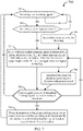
- FIG. 7 shows a flow diagram of an illustrative method 700 for time-limited carrier phase tracking in a phase detector of a clock circuit, according to various embodiments.
- some or all steps of the method 700 are performed iteratively for each operating cycle of the clock circuit (e.g., a PLL).
- some or all steps of the method 700 are performed only after resetting of the phase tracking signals.
- some such embodiments 700 can begin at stage 701 by determining whether the phase tracking signals have been reset (e.g., by assertion of a reset signal that resets edge triggering flip-flops of the phase detector).
- some or all other steps of the method 700 are performed only after such a reset occurs, and the method 700 continues to wait for such a reset otherwise. In other embodiments, some or all steps of the method 700 are performed iteratively for each operating cycle of the clock circuit only where the method is enabled. For example, some such embodiments 700 can begin at stage 702 by determining whether a time-delay enable signal (e.g., time-delay enable signal 331) is asserted, and performing some or all other steps of the method 700 only when the time-delay enable signal is asserted.
- a time-delay enable signal e.g., time-delay enable signal 331
- Some embodiments of the method 700 begin at stage 704 by detecting whether a phase tracking signal (e.g., the first and/or second phase tracking signal 215) is asserted (e.g., for the operating cycle) by a phase detector.
- the phase tracking signal indicates a detected phase difference between an output signal of the PLL (e.g., PLL_fdbk 207) and an input reference signal of the PLL (e.g., PLLin 205).
- embodiments can determine, automatically responsive to detecting that the phase tracking signal is asserted, whether a signal duration of the phase tracking signal exceeds a threshold duration. If not, embodiments can return to an appropriate stage of the method 700 (e.g., waiting for a reset in anticipation of the next operating cycle by returning to stage 701, continuing to detect whether the signal duration has exceeded the threshold duration at stage 704, etc.).
- embodiments can force de-assertion of the phase tracking signal at stage 712 (e.g., for a remainder of the operating cycle and/or until a reset occurs).
- the detection in stage 708 of the signal duration of the phase tracking signal exceeding the threshold duration can cause assertion of a gate trigger signal 345, which can be used to gate the phase tracking signals 215.
- the method 700 can ensure that the phase tracking signal 215 do not remain asserted beyond the threshold duration.
- the method 700 can include determining the threshold duration according to a duration adjustment signal.
- the threshold duration is adjustable by the duration adjustment signal.
- the method 700 can reset a delay timer. In such embodiments, the delay time can be set with the threshold duration and can facilitate the determination in stage 708.
- a first element, component, discussed below could be termed a second element, component, without departing from the teachings of the present invention.
- the terms “logic low,” “low state,” “low level,” “logic low level,” “low,” or “0” are used interchangeably.
- logic high “high state,” “high level,” “logic high level,” “high,” or “1” are used interchangeably.
- the terms “a”, “an” and “the” may include singular and plural references. It will be further understood that the terms “comprising”, “including”, having” and variants thereof, when used in this specification, specify the presence of stated features, steps, operations, elements, and/or components, but do not preclude the presence or addition of one or more other features, steps, operations, elements, components, and/or groups thereof. In contrast, the term “consisting of' when used in this specification, specifies the stated features, steps, operations, elements, and/or components, and precludes additional features, steps, operations, elements and/or components. Furthermore, as used herein, the words “and/or” may refer to and encompass any possible combinations of one or more of the associated listed items.
Landscapes
- Engineering & Computer Science (AREA)
- Computer Networks & Wireless Communication (AREA)
- Signal Processing (AREA)
- Health & Medical Sciences (AREA)
- Toxicology (AREA)
- Physics & Mathematics (AREA)
- General Health & Medical Sciences (AREA)
- Artificial Intelligence (AREA)
- Computer Vision & Pattern Recognition (AREA)
- General Physics & Mathematics (AREA)
- Theoretical Computer Science (AREA)
- Electromagnetism (AREA)
- Computer Security & Cryptography (AREA)
- Stabilization Of Oscillater, Synchronisation, Frequency Synthesizers (AREA)
Abstract
Description
- The present invention relates generally to clock recovery circuits. More particularly, embodiments relate to rapid and accurate tracking of a radiofrequency (RF) carrier for amplitude-modulated signals in unstable reference clock environments, such as for phase-lock loop (PLL) circuits integrated in mobile electronic devices for use with near-field communication (NFC) card emulation (CE) mode communications.
- Various types of short-range radiofrequency (RF) communications are becoming ubiquitous for a wide range of applications, such as for contactless access cards, contactless payment cards, contactless interfaces between devices and peripherals, etc. Near-Field Communications (NFC) is one such RF communications technology that uses inductive coupling between devices to effect contactless exchange of data between devices over a short range (e.g., around 1.5 inches). Many NFC applications support passive NFC devices, such as a passive card or a passive tag. In such applications, the passive device includes one or more integrated chips and an integrated antenna, but no battery. When the passive device is being read by an active reader device, the reader sends a command transmission over an RF carrier (typically by amplitude shift key (ASK) modulation of the carrier signal). The RF carrier induces a current in the antenna of the passive device, which can be harvested by the passive device to power and clock its integrated chip(s). The activated chip(s) can then automatically respond by sending back a signal over the RF carrier, with the response signal being actively modulated according to data stored on the passive device. The reader can detect and process the response signal to recover the transmitted data.
- In such a passive NFC transaction, operation of the passive device may rely on generating and maintaining a reliable clock that accurately tracks the RF carrier. However, in some modes of operation, RF carrier tends not to provide a reliable clock reference for the passive device. For example, in a so-called card emulation (CE) mode, a smart phone, or portable electronic device is configured to emulate a passive NFC device. The portable electronic device may have a relatively small antenna, such that only a small signal level is received from the reader; and the portable electronic device may rely on phase-lock loops (PLLs) or other clock circuits to generate a stable and accurate internal clock signal from the received small-signal RF carrier. In such cases, the ASK modulation of the RF carrier by the reader, and/or active load modulation (ALM) by the passive device can tend to limit the ability of the passive device to generate and maintain an accurate internal clock signal from the RF carrier.
- Embodiments provide circuits, devices, and methods for accurate tracking of a radiofrequency (RF) carrier for amplitude-modulated RF signals in unstable reference clock environments. For example, some embodiments can operate in context of phase-lock loop (PLL) circuits integrated in mobile electronic devices for use with a near-field communication (NFC) card emulation (CE) mode of operation. During operation, the RF carrier can become an unreliable clock reference for an emulated-passive device (i.e., an electronic device operating in NFC CE mode) due, for example, to amplitude modulation of the RF carrier by the reader, and/or to active load modulation of the RF carrier by the emulated-passive device. It can be desirable to stop the PLL from tracking the RF carrier during times when the RF carrier is unreliable (i.e., as a clock reference). However, it can take time to detect that the RF carrier has become unreliable, leaving a time window during which the PLL continues to track an unreliable reference. Embodiments described herein seek to limit the amount of phase and/or frequency error introduced in the PLL output while tracking an unreliable reference. For example, during tracking, a PLL typically asserts phase tracking signals to maintain phase alignment between its output and its input reference. Embodiments can provide adjustable time-limited gating of those phase tracking signals, thereby limiting the amount of change in phase introduced by the PLL.
- According to one set of embodiments, a time limiter circuit is provided for integration with a phase detector of a phase-locked loop (PLL). The time limiter circuit includes: an absolute phase detection sub-circuit to detect whether a phase tracking signal is asserted by the phase detector, the phase tracking signal indicating a detected phase difference between an output signal of the PLL and an input reference signal of the PLL; a delay timer sub-circuit, coupled with the absolute phase detection sub-circuit to determine, automatically responsive to the absolute phase detection sub-circuit detecting that the phase tracking signal is asserted, whether a signal duration of the phase tracking signal exceeds a threshold duration; and a pulse gating sub-circuit, coupled with the delay timer sub-circuit to force de-assertion of the phase tracking signal for at least a remainder of a present operating cycle of the PLL automatically responsive to the delay timer sub-circuit determining that the signal duration exceeds the threshold duration.
- According to another set of embodiments, a phase-locked loop (PLL) circuit is provided. The PLL circuit includes: a PLL input node to receive a reference clock signal; a PLL output node to output a generated clock signal; and a phase detector, coupled with the PLL input node and the PLL output node to generate a phase tracking signal indicating a phase difference between the reference clock signal and the generated clock signal. The phase tracking signal includes a first phase tracking signal responsive to a phase of the reference clock signal preceding a phase of the generated clock signal, and a second phase tracking signal responsive to the phase of the generated clock signal preceding the phase of the reference clock signal. The phase detector has a time limiter circuit, including: an absolute phase detection sub-circuit to detect whether the phase tracking signal is asserted by the phase detector; a delay timer sub-circuit, coupled with the absolute phase detection sub-circuit to determine, automatically responsive to the absolute phase detection sub-circuit detecting that the phase tracking signal is asserted, whether a signal duration of the phase tracking signal exceeds a threshold duration; and a pulse gating sub-circuit, coupled with the delay timer sub-circuit to force de-assertion of the phase tracking signal for a remainder of at least a present operating cycle of the PLL automatically responsive to the delay timer sub-circuit determining that the signal duration exceeds the threshold duration. In some such embodiments, a portable electronic device is provided, having the PLL circuit integrated therein, wherein: the portable electronic device is associated with stored data and comprises an active load modulation circuit configured to generate a response signal based on active load modulation of the generated clock signal in accordance with a near field communication (NFC) card emulation (CE) mode of operation
- According to another set of embodiments, a method is provided. The method includes: detecting whether a phase tracking signal is asserted by a phase detector of the PLL, the phase tracking signal indicating a detected phase difference between an output signal of the PLL and an input reference signal of the PLL; determining, automatically responsive to detecting that the phase tracking signal is asserted, whether a signal duration of the phase tracking signal exceeds a threshold duration; and forcing de-assertion of the phase tracking signal for a remainder of a present operating cycle of the PLL automatically responsive to determining that the signal duration exceeds the threshold duration.
- The accompanying drawings, referred to herein and constituting a part hereof, illustrate embodiments of the disclosure. The drawings together with the description serve to explain the principles of the invention.
-
FIG. 1 shows an illustrative Near-Field Communications (NFC) transaction environment with a device operating in a so-called card emulation (CE) mode, as context for various embodiments described herein; -
FIG. 2A shows an illustrative phase-locked-loop (PLL) circuit, as context for various embodiments; -
FIG. 2B shows an illustrative implementation of a conventional phase comparison block; -
FIG. 3 shows an illustrative novel phase detector, according to various embodiments; -
FIG. 4 shows an illustrative circuit implementation of a time limiter for integration in a phase comparison block of a clock module, according to various embodiments; -
FIGS. 5 and6 , which show illustrative plots of various signals of a phase detector having a novel time limiter, as described herein; and -
FIG. 7 shows a flow diagram of an illustrative method for time-limited carrier phase tracking in a phase detector of a clock circuit, according to various embodiments. - In the appended figures, similar components and/or features can have the same reference label. Further, various components of the same type can be distinguished by following the reference label by a second label that distinguishes among the similar components. If only the first reference label is used in the specification, the description is applicable to any one of the similar components having the same first reference label irrespective of the second reference label.
- In the following description, numerous specific details are provided for a thorough understanding of the present invention. However, it should be appreciated by those of skill in the art that the present invention may be realized without one or more of these details. In other examples, features and techniques known in the art will not be described for purposes of brevity.
- Various types of short-range radiofrequency (RF) communications are becoming ubiquitous for a wide range of applications. For example, passive, contactless data devices are being used to authorize access to secure facilities, to effect electronic payment transactions at points of sale, to withdraw cash at automated teller machines, to quickly register and/or connect peripherals (e.g., headphones, printers, drives, etc.) to electronic devices, etc. Near-Field Communications (NFC) is one such RF communications technology that uses inductive coupling between devices to effect contactless exchange of data between devices over a short range (e.g., around 1.5 inches). Many NFC applications support passive NFC devices, such as a passive card or a passive tag. In such applications, the passive device includes one or more integrated chips and an integrated antenna, but no battery. When the passive device is being read by an active reader device, the reader sends a command transmission over an RF carrier (typically by amplitude shift key (ASK) modulation of the carrier signal). The RF carrier induces a current in the antenna of the passive device, which can be harvested by the passive device to power and clock its integrated chip(s). The activated chip(s) can then automatically respond by sending back a signal over the RF carrier, with the response signal being actively modulated according to data stored on the passive device. The reader can detect and process the response signal to recover the transmitted data. In such a passive NFC transaction, operation of the passive device may rely on generating and maintaining a reliable clock that accurately tracks the RF carrier. However, in some modes of operation, RF carrier tends not to provide a reliable clock reference for the passive device.
- For the sake of illustration,
FIG. 1 shows an illustrative Near-Field Communications (NFC) transaction environment with a device operating in a so-called card emulation (CE) mode, as context for various embodiments described herein. TheCE device 120 can be a smart phone, wearable device (e.g., smart watch or fitness tracker), or any other suitable portable electronic device. In this context, theCE device 120 is typically an active device, but theCE device 120 is configured to operate in a mode in which it emulates a passive NFC device, such as a passive contactless card or tag. For example, a smart phone can be configured to support the NFC CE mode of operation, so that it can be used to effect mobile payment transactions, and the like, even while powered off, or in standby power mode. - As described above, a typical NFC transaction can involve the
CE device 120 being read by areader 110, such as an electronic lock, point of sale terminal, etc. Thereader 110 can broadcast a signal over an ASK-modulatedRF carrier 115, typically at 13.56 Megahertz. TheRF carrier 115 induces a current in anantenna 130 of theCE device 120, and theantenna 130 can be configured specifically for NFC communications. As illustrated,antenna 130 of theCE device 120 can be coupled with one or more integrated circuits and/or data storage. In some implementations, some or all of the integrated circuits are dedicated circuits for implementing the NFC CE mode of operation, such as by including an integrated NFC (or NFC CE mode) chipset into a smart phone. In other implementations, some or all of the integrated circuits are implemented by multi-functional components of theCE device 120, such as by the main processors and/or other circuits of a smart phone. The integrated circuits can implement some or all of ademodulator module 140, a power regulator and/or recovery (PRR)module 145, aclock module 150, acontroller module 160, and an active load modulation (ALM)module 165. Thecontroller module 160 and/or other modules of theCE device 120 can include, or be implemented with, a central processing unit CPU, an application-specific integrated circuit (ASIC), an application-specific instruction-set processor (ASIP), a digital signal processor (DSP), a field-programmable gate array (FPGA), a programmable logic device (PLD), a controller, a microcontroller unit, a reduced instruction set (RISC) processor, a complex instruction set processor (CISC), a microprocessor, or the like, or any combination thereof. In some cases, data communicated by theCE device 120 in NFC CE mode is stored in on-board data storage 155 of theCE device 120, such as in a so-called secure element. In other cases, some or all of the data is stored off-board theCE device 120, such as in so-called Host Card Emulation (HCE) implementations, or the like. - In a typical operational example, the
RF carrier 115 induces a current signal in theantenna 130 of theCE device 120. The energy from the current signal can be harvested and regulated by thePRR module 145 to power other component modules. In a typical NFC reader/writer mode with a passive device, there may be no power source at all, such that all the power for operation must be harvested from the receivedRF carrier 115. In NFC CE mode, theCE device 120 typically includes apower source 147, such as an integrated battery. However, it is desirable that, when operating in NFC CE mode, theCE device 120 draws minimal power from the integratedpower source 147. - The current signal induced from the
RF carrier 115 can also be demodulated by thedemodulator module 140 and used by theclock module 150 to generate an internal clocking signal (or multiple clocking signals). As described herein, it is desirable for the internal clocking signal to track theRF carrier 115, so that the internal clocking signal can be used to generate a response transmission from theCE device 120 back to thereader 110. The internal clocking signal can also be used to clock other components, such as thecontroller module 160 and theALM module 165. For example, thecontroller module 160 controls operation of one or more components of the system in NFC CE mode, while being powered at least partially by harvested power output by the PRR module, and while being clocked by the internal clocking signal output by theclock module 150. In such a manner, thecontroller module 160 can direct theALM module 165 to actively modulate the internal clocking signal by switching a load (e.g., by switching a power amplifier on and off) in accordance with particular data associated with theCE device 120. For example, the active load modulation of the internal clocking signal can be used to communicate identification codes, biometric data, image data, etc. - The output of the
ALM module 165 is anALM response signal 125 generate by the active load modulation of the internal clocking signal output. The generatedALM response signal 125 is used to drive theantenna 130, such that theantenna 130 broadcasts the ALM response signal 125 (e.g., at the same carrier frequency of 13.56 Megahertz) back to thereader 110. Thus, in a typical NFC CE mode transaction, theCE device 120 detects broadcast of the ASK-modulatedRF carrier 115 signal from thereader 110 and automatically responds with a broadcast of theALM response signal 125. The reader can detect and process the responseALM response signal 125 to recover the transmitted data, from which thereader 110 can make suitable determinations, such as whether to authorize access, to authorize a payment transaction, to effect a further data exchange, etc. - It is notable that the
reader 110 and theCE device 120 rely on specific carrier frequencies for their communications, such that effective transacting may rely on theCE device 120 being able to generate and maintain a reliable internal clock signal that accurately tracks the receivedRF carrier 115. However, particularly in NFC CE mode, theRF carrier 115 tends not to provide a reliable clock reference for theCE device 120. For example, in NFC reader/writer mode, dedicated passive smart cards and/or smart tags are often implemented with relatively large antennas capable of receiving a relatively large signal level, and dedicated passive smart cards and/or smart tags typically use so-called passive load modulation (PLM) instead of ALM. For at least those reasons, such dedicated passive devices are typically able to generate a sufficiently reliable internal clock signal from the receivedRF carrier 115. However,CE devices 120 often include appreciably smaller antennas (e.g., antenna 130), which tend to receive an appreciably smaller signal level. As such, it can be desirable for theclock module 150 of aCE device 120 to include more complex clock circuits to assist with generating a stable and accurate internal clock signal from the received small-signal RF carrier 115, while drawing only minimal power from thepower source 147. Embodiments of theclock module 150 include a phase-locked loop (PLL). PLLs operated by dynamically controlling loop parameters in an attempt to maintain tracking between their generated output and a received reference. - For added context,
FIG. 2A shows an illustrative phase-locked-loop (PLL)circuit 200. ThePLL circuit 200 generates a PLL output signal (PLL_out) 240 in accordance with a received PLL input signal (PLL_in) 205. For example,PLL_in 205 can be a clock reference signal received from theRF carrier 115 at the NFC carrier frequency. ThePLL circuit 200 uses a feedback loop to generatePLL_out 240 in an attempt to keepPLL_out 240 locked to a desired output frequency (e.g., the frequency ofPLL_in 205, or a whole or fractional multiple of the input frequency of PLL_in 205). As illustrated, thePLL circuit 200 includes aphase comparison block 210, aloop filter block 220, a voltage controlledoscillator block 230. Some implementations also include adivider block 250. - The
phase comparison block 210 can be implemented as a phase/frequency detector (PFD), or any other suitable component, that receivesPLL_in 205 at an input reference frequency (f REF) and comparesPLL_in 205 with a signal fed back by the feedback loop of thePLL circuit 200. The fed back signal (PLL_fdbk 207) is at a feedback frequency (f FDBK). The output of thephase comparison block 210 is a function of the comparison and is fed to theloop filter block 220. Theloop filter block 220 can include any suitable components for facilitating filtering over the feedback loop, such as a charge pump and a low-pass filter. In some implementations, the charge pump is implemented as part of thephase comparison block 210 and used to drive theloop filter 220. - The output of the
loop filter block 220 can be used as a control voltage for controlling theVCO block 230. TheVCO block 230 can include any suitable oscillator, such as an inductive-capacitive (LC) oscillator, a ring oscillator, etc. The output frequency of the PLL circuit 200 (i.e., the frequency of PLL_out 240), or f OUT, can therefore by controlled at least partially by theVCO block 230. In some implementations,PLL_out 240 is fed directly back to thephase comparison block 210 to complete the feedback loop of thePLL circuit 200. In other implementations, f OUT is further a function of a dividing value associated with adivider block 250. For example, if thedivider block 250 is designed to divide f OUT by N (e.g., where N is a non-zero integer), thePLL circuit 200 will seek to lock f OUT to a frequency that is N times f REF (the frequency of PLL_in 205). In that way, the dividing value associated with thedivider block 250 can effectively define the mathematical relationship between the frequencies ofPLL_out 240 andPLL_in 205, thereby effectively controlling f OUT. Embodiments described herein generally assume that thePLL circuit 200 is configured to generate thePLL_out 240 to track the frequency and phase of the PLL_in 205 (i.e., that the generated internal clocking signal tracks the RF carrier 115). As such, thePLL circuit 200 of theclock module 150 ofFIG. 1 may be implemented without adivider block 250, or with N = 1. - For further context,
FIG. 2B shows an illustrative implementation of a conventional phase comparison block 210 (labeled as 210'). A first flip-flop 212a is configured as an edge detector for detecting a rising edge of PLL_in 205 (the clock reference signal), and a second flip-flop 212b is configured as an edge detector for detecting a rising edge of PLL_fdbk 207 (the loop feedback signal corresponding to the generated internal clocking signal). When the first flip-flop 212a is triggered, it outputs (and holds) a firstphase tracking signal 215a (e.g., an "up" signal). When the second flip-flop 212b is triggered, it outputs (and holds) a secondphase tracking signal 215b (e.g., a "down" signal). The first and second phase tracking signals 215 are coupled with acharge pump 214 that generated a loop filtercurrent output 217. In particular, the firstphase tracking signal 215a couples a first current source to the loop filtercurrent output 217 that increases the amount of current being pumped to the loop filter, and the secondphase tracking signal 215b couples a second current source to the loop filtercurrent output 217 that decreases the amount of current being pumped to the loop filter. The phase tracking signals 215 are both coupled with an ANDgate 216, which outputs areset signal 209. As such, when both phase tracking signals 215 are asserted (i.e., rising edges are detected by both flip flops 212), thereset signal 209 is asserted, causing the flip-flops 212 to reset until the next PLL loop cycle. - As used herein, terms like "asserting" a signal, the signal is "asserted," are intended generally to indicate setting a signal to a logical value that indicates presence of a particular associated condition. In some embodiments, a signal is asserted by having a logical value of HIGH, TRUE, or '1', or the like; such as by holding the signal at a particular voltage level associated with that logical value. For example, each illustrated flip-flop 212 is illustrated as configured to assert a respective phase tracking signal 215 by switching the phase tracking signal 215 to a HIGH voltage level at its "Q" output responsive to detecting a rising edge of a triggering signal received at its input (i.e., either
PLL_in 205 or PLL_fdbk 207). However, those of skill in the art will recognize that, with trivial variations to implementations illustrated and described herein, particular signals will be considered "asserted" when they are set to a logical LOW, FALSE, '0', or the like. For example, coupling each respective phase tracking signal 215 to a Q-bar output (complement of Q) of its associated flip flop 212, and adding a NOT gate in the path to thecharge pump 214, results in an essentially equivalent circuit where the phase tracking signals 215 are "asserted" by setting their value to '0'. - In effect, if the phase of
PLL_in 205 is left-shifted relative to (i.e., faster than that of)PLL_fdbk 207, the first flip-flop 212a will trigger first, thereby asserting the firstphase tracking signal 215a (the "up" signal). While the firstphase tracking signal 215a is asserted, more current is pumped into theloop filter 220 viacharge pump 214 to compensate for the phase difference. When thePLL_fdbk 207 edge is detected by the second flip-flop 212b, the secondphase tracking signal 215b is momentarily asserted, causing the ANDgate 216 to assert thereset signal 209, and resetting the flip-flops 212 (and de-asserting the phase tracking signals 215). As a corollary, if the phase ofPLL_fdbk 207 is left-shifted relative to (i.e., faster than that of) PLL in 205, the second flip-flop 212b will trigger first, thereby asserting the secondphase tracking signal 215b (the "down" signal). While the secondphase tracking signal 215b is asserted, current is reduced to theloop filter 220 viacharge pump 214 to compensate for the phase difference. When thePLL_in 205 edge is detected by the first flip-flop 212a, the firstphase tracking signal 215a is momentarily asserted, causing the ANDgate 216 to assert thereset signal 209, and resetting the flip-flops 212 (and de-asserting the phase tracking signals 215). - As described above, PLL operation typically involves dynamic adjustment of loop parameters to maintain tracking of the output signal to the input reference. The described conventional phase tracking (e.g., according to
FIG. 2B ) tends to work well, as long as there is a stable clock reference at the input of the PLL by which to track. In the case of NFC CE mode, however, the input reference is typically the signal on theantenna 130, which can be unreliable. For example, when theCE device 120 is receiving, the signal on the antenna (the RF carrier 115) is being ASK-modulated, such that the clock reference for the PLL toggles unpredictably between being present and being absent (i.e., assuming typical 100-percent ASK modulation used by NFC readers). Similarly, when theCE device 120 is transmitting, the signal on the antenna (the ALM response signal 125) is being actively load-modulated, such that the amplitude of the signal changes in accordance with the data signal. If the PLL is used to track an unreliable clock reference, the output of the PLL will similarly be an unreliable output signal. For example, there could be large swings in phase and frequency error (relative to the desired carrier phase and frequency) during the times when the clock reference becomes unreliable, and as the PLL attempts to regain tracking when the reliable clock reference returns. - As such, some phase comparison blocks 210 are configured to selectively switch the PLL between open-loop and closed-loop modes based on the reliability of the clock reference. While the clock reference is reliable, it is desirable for the PLL to operate in the closed-loop mode, whereby the PLL output is tracked to the clock reference at its input by dynamically updating loop parameters. While the clock reference is unreliable, it is desirable for the PLL to operate in the open-loop mode, whereby the PLL output is not tracked to the clock reference at its input; instead maintaining its loop parameters in a last-updated condition. As illustrated, implementations can include a
pause signal 211 that is asserted responsive to detecting the carrier being in an unreliable condition. In such implementations, the output of the ANDgate 216 and thepause signal 211 can be inputs to anOR gate 218, which outputs thereset signal 209. For example, when the clock reference is unreliable, thepause signal 211 is asserted, thereby holding the flip-flops 212 in a reset state. There is no edge triggering, no assertion of the phase tracking signals 215, and no adjustment to the current supplied to theloop filter 220. As such, while thepause signal 211 is asserted, there is an effective de-coupling of the unreliable clock reference from loop parameter adjustments, and the PLL operates in an open-loop manner. - Once the clock reference is determined to be unreliable, asserting such a
pause signal 211 can be an effective approach to triggering open-loop operation of the PLL. However, in some cases, it can be difficult to detect precisely when the clock reference becomes unreliable. For example, in the NFC CE mode, thecontroller module 160 of theCE device 120 can be used to detect the loss of a reliable reference signal and can assert thepause signal 211 as a control signal to theclock module 150. However, particularly while receiving theRF carrier 115 from thereader 110, there may be no way for thecontroller module 160 to know exactly when the ASK-modulatedRF carrier 115 will suddenly disappear. Moreover, when the ASK modulation switches between HIGH and LOW, there is typically a period of time when there continues to be an induced signal in theantenna 130, but the signal effectively has a random phase; the reference is thus unreliable during that timeframe. For these and other reasons, there is typically a delay between the moment at which the clock reference becomes unreliable and the time when the PLL is triggered to operate in an open-loop manner. Even when that delay is relatively short, appreciable phase error can be introduced into the internal clocking signal. A similar effect can also occur when switching back to closed-loop operation. For example, there may be no way for thecontroller module 160 to know exactly when the ASK-modulatedRF carrier 115 will suddenly reappear, and/or when the induced signal in theantenna 130 will settle back to a reliable clock reference. For these and other reasons, there is typically another delay between the moment at which the clock reference becomes reliable and the time when the PLL is triggered to operate in the closed-loop manner. Further, as described herein, when the PLL back is switched back to closed-loop mode, it can initially make incorrect tracking decisions, which can cause further delay until the PLL is accurately locked back onto the again-reliable clock reference. - In the NFC CE operating mode, successful operation can rely on accurate carrier tracking during all communication phases, including during a guard time phase, a frame delay time (FDT) phase, command reception phase, and an ALM phase. Some applications have associated operational constraints (e.g., specified by standards, or the like) for such carrier tracking. For example, a NFC CE mode application may be required to operate with a phase drift of less than a few degrees (e.g., less than five degrees), even when the command reception phase and/or ALM phase times are relatively long (e.g., appreciably longer than ten milliseconds). Such tracking can generally be straightforward during the guard time and frame delay time, where the
RF carrier 115 tends to remain reliable. However, as described herein, such tracking becomes more difficult in the command reception phase due to the ASK modulation of theRF carrier 115, and in the ALM phase due to active load modulation of theALM response signal 125. Further, based on the above, there are at least three timeframes of concern involved with maintaining accurate tracking of a desired carrier in context of an unreliable clock reference, such as during the command reception phase and the ALM phase. The first timeframe begins when the clock reference becomes unreliable and ends when the PLL enters open loop mode and stops tracking, during which time a conventional PLL would continue to track the unreliable clock reference. The second is the timeframe during which the PLL is running open loop, during which the PLL can tend to drift in frequency and/or phase. The third timeframe begins when the PLL is returned to closed mode and begins tracking to the clock reference and ends when the PLL successfully locks back onto the reference phase and frequency. - Some embodiments described herein seek to address concerns involved with the first timeframe. In a typical NFC CE implementation, such embodiments may tend to be most applicable to the command reception phase, when the ASK modulation of the
RF carrier 115 causes the reliability of the carrier as a clock reference to be unpredictable. In contrast, during the ALM phase, the CE device 120 (e.g., thecontroller module 160 and/or the ALM module 165) typically controls when and how the carrier is modulated. As such, theCE device 120 can know exactly when the clock reference for the PLL will and will not be reliable, and can accurately control timing of when the PLL operates in open-loop and closed-loop modes. Such timing can be carefully controlled to substantially eliminate any delay between the clock reference becoming unreliable and the PLL entering open loop mode, thereby substantially eliminating effects of the first timeframe. Still, embodiments described herein can be applied to any suitable phase of any suitable communication environment in which aclock module 150 seeks to maintain tracking with an unpredictably unreliable clock reference. -
FIG. 3 shows an illustrativenovel phase detector 300, according to various embodiments. Thephase detector 300 can be an implementation of the phase comparison block 210 of thePLL circuit 200 ofFIG. 2 , which can be included in an implementation of theclock module 150 of theCE device 120 ofFIG. 1 . As illustrated, embodiments of thephase detector 300 include anedge detector 310, atime limiter 320, and acharge pump 214. In some embodiments, theedge detector 310 and thecharge pump 214 include similar components to, and operate in a similar manner to, similarly labeled components of the phase comparison block 210' ofFIG. 2B . As described above, theedge detector 310 can use flip-flops 212, or other suitable components, to detect an edge (e.g., a rising edge) of aPLL_in 205 signal (the clock reference signal) and aPLL_fdbk 207 signal (feedback from the internal clocking signal generated by the PLL). When thePLL_in 205 edge is detected, a firstphase tracking signal 215a is asserted; when aPLL_fdbk 207 edge is detected, a secondphase tracking signal 215b is asserted; and when both phase tracking signals 215 are asserted, a set of logic gates (ANDgate 216 and OR gate 218) assert a reset signal to reset the flip flops 212 until the next loop iteration of the PLL. As illustrated, implementations can also include apause signal 211, which can effectively stop thephase detector 300 from tracking to the clock reference, thereby setting the PLL to operate in an open-loop mode. - In the conventional implementation shown in
FIG. 2B , the phase tracking signals 215 asserted by the flip-flops 212 directly control thecharge pump 214. For example, assertion of the firstphase tracking signal 215a corresponds to PLL_fdbk 207 laggingPLL_in 205, which directly causes a compensating increase in loop filter current at acharge pump output 317; and the secondphase tracking signal 215b corresponds to PLL_fdbk 207 leadingPLL_in 205, which directly causes a compensating decrease in loop filter current at acharge pump output 317. However, when the PLL is tracking an unreliable clock reference, this can result in appreciable phase and frequency error (e.g., until thepause signal 211 is ultimately asserted). In thenovel phase detector 300 ofFIG. 3 , embodiments of thetime limiter 320 can limit the impact of any phase tracking signal 215, thereby limiting the amount of phase and frequency error that can be introduced into the internal clocking signal in the event of the PLL tracking an unreliable clock reference. - As illustrated, the
time limiter 320 can include an absolute phase detection (APD) sub-circuit 330, adelay timer sub-circuit 340, and apulse gating sub-circuit 350. Embodiments of the APD sub-circuit 330 can detect whether a phase tracking signal 215 (one of the first or the second phase tracking signals 215) is asserted by theedge detector 310 in a present operating cycle of the PLL. As described herein, the phase tracking signal 215 indicates a detected phase difference betweenPLL_fdbk 207 andPLLin 205. The APD sub-circuit 330 can output anabsolute phase signal 335 responsive to detecting a phase difference betweenPLL_fdbk 207 andPLL_in 205 based on the phase tracking signal 215, such that theabsolute phase signal 335 is asserted regardless of the direction of the phase difference (i.e., regardless of whetherPLL_fdbk 207 is leading or lagging PLL_in 205). For example, theabsolute phase signal 335 automatically goes HIGH whenever either of the phase tracking signals 215 is HIGH, and theabsolute phase signal 335 automatically becomes de-asserted (returns to LOW) when there is a reset of the phase tracking signals 215. - Embodiments of the
delay timer sub-circuit 340 are coupled with the APD sub-circuit 330 to determine whether a signal duration of an asserted phase tracking signal 215 exceeds a threshold duration. In some embodiments, the threshold duration is fixed, for example, by being hard-coded into circuitry of thedelay timer sub-circuit 340. In other embodiments, the threshold duration is adjustable. The illustrated embodiment shows thedelay timer sub-circuit 340 coupled with a control input node to receive aduration adjustment signal 341, and theduration adjustment signal 341 can effectively set the threshold duration. Such setting can be accomplished in any suitable manner. In one implementation, theduration adjustment signal 341 is hardware- or firmware-controlled, such as using switches, transistors, programmable firmware, etc. In another implementation, theduration adjustment signal 341 is dynamically controllable by software, by thecontroller module 160, etc. For example, a value associated with theduration adjustment signal 341 can be set in a software environment of theCE device 120, which thereby adjusts the threshold duration. - In some implementations, the APD sub-circuit 330 determines whether the signal duration exceeds the threshold duration based on the
absolute phase signal 335. For example, when theabsolute phase signal 335 is asserted, a delay time begins to record a duration during which theabsolute phase signal 335 is asserted. If thedelay timer sub-circuit 340 detects that the duration has reached or exceeded a threshold duration, thedelay timer sub-circuit 340 can assert agate trigger signal 345. As illustrated, embodiments of thedelay timer sub-circuit 340 are coupled with thereset signal 209, so that thegate trigger signal 345 is effectively reset along with the phase tracking signals 215. Typically, the time-limiting functionality is in effect when the clock reference is unreliable, such as when the RF carrier is absent. At such times, there may be no edge ofPLL_in 205 to detect, so that there may be no reset of the phase tracking signals 215 (e.g., until the clock reference becomes present again). In other cases, the RF carrier may not be absent; rather it may be otherwise unreliable (e.g., having indeterminate phase, etc.). In such cases, in each loop iteration of the PLL, theabsolute phase signal 335 can be asserted from when a first rising edge is detected (i.e., of the faster ofPLL_in 205 orPLL_fdbk 207 in that loop iteration) until a next rising edge is detected (i.e., of the slower ofPLL_in 205 orPLL_fdbk 207 in that loop iteration), at which point a reset of the phase tracking signals 215 is triggered by theedge detector 310. Similarly, it can be seen that, in each loop iteration of the PLL, thegate trigger signal 345 may be asserted from when assertion of theabsolute phase signal 335 first exceeds the threshold duration until thereset signal 209 is asserted for that loop iteration indicating a reset of the phase tracking signals 215. - Embodiments of the
pulse gating sub-circuit 350 are coupled with thedelay timer sub-circuit 340 to gate the duration of any phase tracking signal 215 that is asserted beyond the threshold duration controlled by thedelay timer sub-circuit 340. In some embodiments, the pulse gating sub-circuit 350 forces de-assertion of any asserted phase tracking signal 215 until a next reset of the flip-flops 212 occurs (e.g., at least for a remainder of the present loop iteration of the PLL) automatically responsive to assertion of thegate trigger signal 345 by thedelay timer sub-circuit 340. The output of thepulse gating sub-circuit 350 is a time-limited set of phase tracking signals 215, indicated as phase tracking signals 215'. The time-limited set of phase tracking signals 215' can be used to control thecharge pump 214. In effect, each time-limited phase tracking signal 215' can be equal to a corresponding one of the phase tracking signals 215, but only as long as its duration does not exceed the threshold duration. For example, a first time-limitedphase tracking signal 215a' is HIGH only when the corresponding firstphase tracking signal 215a is HIGH and thegate trigger signal 345 is LOW; when thegate trigger signal 345 is HIGH, the first time-limitedphase tracking signal 215a' is LOW, regardless of the state of the corresponding firstphase tracking signal 215a. - In some embodiments, the
time limiter 320 includes an enable input node to receive a time-delay enablesignal 331. In the illustrated implementation, the time-delay enablesignal 331 is coupled with the APD sub-circuit 330, which can effectively disable thetime limiter 320. With such an implementation, when the time-delay enablesignal 331 is de-asserted, the APD sub-circuit 330 is effectively disabled, such that there is no assertion of theabsolute phase signal 335. As such, theabsolute phase signal 335 cannot exceed the threshold duration, such that there will not be any assertion of thegate trigger signal 345, and the time-limited set of phase tracking signals 215 will always follow their corresponding phase tracking signals 215. Other implementations can use the time-delay enablesignal 331 in any other suitable manner to provide for selective enabling and disabling of thetime limiter 320. In one such implementation, the time-delay enablesignal 331 is coupled with thedelay timer sub-circuit 340 to hold thegate trigger signal 345 in a de-asserted state when the time-delay enablesignal 331 is de-asserted. - Some implementations use the time-delay enable
signal 331 to selectively disable thetime limiter 320 during certain phases of operation. As noted above, a result of thetime limiter 320 can be to limit the ability of the PLL to dynamically adjust in any one or more operating cycles, thereby minimizing the amount of phase and/or frequency drift that can occur while tracking an unreliable reference. However, in some phases of operation, limiting the PLL's ability to dynamically adjust can cause an undesirable slowing of the PLL functionality. For example, during startup of the PLL, or otherwise when the PLL is seeking to lock onto a clock reference, it can be desirable for such locking to occur as quickly as possible. Disabling thetime limiter 320 during those phases can allow the PLL larger per-cycle dynamically adjustments, which can allow the PLL to more quickly lock onto the clock reference. - The
time limiter 320 can be implemented using any suitable components in any suitable arrangement.FIG. 4 shows an illustrative circuit implementation of atime limiter 400 for integration in a phase comparison block of aclock module 150, according to various embodiments. For example, thetime limiter 400 can be an implementation of thetime limiter 320 in thephase detector 300 ofFIG. 3 . Theillustrated time limiter 400 circuitry can be integrated in circuitry of other components, implemented as a dedicated integrated circuit, or implemented in any other suitable manner. As shown, thetime limiter 400 can have input and/or output nodes for coupling components of thetime limiter 400 with signal paths, such as signal paths of anedge detector 310 and acharge pump 214. As described with reference toFIG. 3 , thetime limiter 400 can include anAPD sub-circuit 330, adelay timer sub-circuit 340, and apulse gating sub-circuit 350. - The illustrated
APD sub-circuit 330 includes an ORgate 432 having inputs coupled with the phase tracking signals 215, such that theOR gate 432 asserts its output when the first and/or second phase tracking signal 215 is asserted. As such, an asserted signal at the output of theOR gate 432 indicates that there is a phase difference betweenPLL_in 205 andPLL_fdbk 207. In some implementations, the output of theOR gate 432 is used as theabsolute phase signal 335. In other implementations, the APD sub-circuit 330 further includes an ANDgate 434 having inputs coupled with the output of theOR gate 432 and the time-delay enablesignal 331, such that ANDgate 434 asserts its output only when both theOR gate 432 output and the time-delay enablesignal 331 are asserted. In such implementations, the output of the ANDgate 434 is used as theabsolute phase signal 335, such that theabsolute phase signal 335 indicates that there is a phase difference betweenPLL_in 205 andPLL_fdbk 207 and time limiting is enabled. - The illustrated
delay timer sub-circuit 340 can be coupled with the APD sub-circuit 330 via theabsolute phase signal 335. As illustrated, thedelay timer sub-circuit 340 can include a number of time delay elements, such as a multiple flip-flops 442 coupled together in a chain. The chain of flip-flops 442 can be clocked by any suitable delaytimer clock signal 443 that is appreciably faster than the output frequency of the PLL (e.g., the carrier frequency). In operation, when theabsolute phase signal 335 is asserted, it is clocked into the first of the chain of flip-flops 442; and assertion of theabsolute phase signal 335 propagates through the chain of flip-flops 442, causing assertion of the output of each subsequent flip flop 442 in the chain with each cycle of the delaytimer clock signal 443. The amount of time it takes for propagation through the entire chain of flip-flops 442 is a function of the number of flip-flops 442 in the chain and the frequency of the delaytimer clock signal 443, which effectively sets the threshold duration (i.e., the chain of flip-flops 442 effectively implement a delay timer set with the threshold duration). If propagation continues through the entire chain of flip-flops 442 until the output of the last flip flop 442 in the chain is ultimately asserted, that output can be used to assert thegate trigger signal 345 as an indication that the full threshold duration has been reached. As illustrated, the chain of flip-flops 442 are coupled with the reset signal 209 (e.g., via a buffer). As such, if a reset occurs in the present operating cycle of the PLL, the flip-flops 442 reset, which effectively resets the delay timer. For example, in a particular operating cycle of the PLL, when either one of the phase tracking signals 215 is asserted, theabsolute phase signal 335 can be asserted, and the assertedabsolute phase signal 335 can start propagating through the chain of flip-flops 442. If the other phase tracking signal 215 is asserted before the propagation reaches the last flip-flop 442 in the chain, a reset is triggered, causing assertion of thereset signal 209 and resetting of the delay timer. However, if the other phase tracking signal 215 is not asserted before the propagation reaches the last flip-flop 442 in the chain, the output of the last flip-flop 442 in the chain will cause thegate trigger signal 345 to become asserted. Thegate trigger signal 345 can remain asserted until a next reset of the flip-flops 212. - In some implementations, as illustrated, the
delay timer sub-circuit 340 includes a selector component, such as amultiplexer 444. Inputs of themultiplexer 444 are coupled with respective outputs of some or all of the flip-flops 442 in the chain, and the output of themultiplexer 444 is a selected one of those inputs, as controlled by theduration adjustment signal 341. In the illustrated implementation, setting theduration adjustment signal 341 effectively controls the length of the chain of flip-flops 442 by selecting which flip-flop 442 output to use for asserting thegate trigger signal 345. Any suitable number of delay components can be included in the chain, depending on the desired range of threshold delays, how finely it is desired to tune the threshold delay, and/or other factors. In some implementations, themultiplexer 444 output is used directly as thegate trigger signal 345. - The illustrated
pulse gating sub-circuit 350 is coupled with thedelay timer sub-circuit 340 via thegate trigger signal 345. As shown, thepulse gating sub-circuit 350 can include an inverter and a pair of AND gates 452. Each AND gate 452 can generate a respective one of the time-limited set of phase tracking signals 215' at its output, responsive to one input being coupled with the complement of thegate trigger signal 345, and another input being coupled with a respective one of the phase tracking signals 215. In such a configuration, each time-limited phase tracking signal 215' is asserted when the corresponding phase tracking signal 215 is asserted and thegate trigger signal 345 is not asserted. For example, each time-limited phase tracking signal 215' is equal to its corresponding phase tracking signal 215, but only as long as its duration does not exceed the threshold duration. When the threshold duration is exceeded, thegate trigger signal 345 forces de-assertion of any asserted time-limited phase tracking signal 215', regardless of whether its corresponding phase tracking signal 215 is asserted. - Such time-limiting of the phase tracking signals 215 can be seen in
FIGS. 5 and6 , which showillustrative plots FIG. 5 , theplots 500 begin in a timeframe when steady state has been reached, such that the clock reference is reliable, and the PLL has locked onto and is accurately tracking the clock reference. For example, the clock reference atPLL_in 205 is faithfully represented byPLL_fdbk 207, corresponding to feedback of thePLLout 240 signal. In such a steady state condition, at each rising edge ofPLLin 205 andPLL_fdbk 207, theedge detector 310 may briefly assert the firstphase tracking signal 215a and the secondphase tracking signal 215b prior to triggering a reset. At the output of thetime limiter 320, the time-limited phase tracking signals 215' may be substantially equivalent to their corresponding phase tracking signals 215, as the durations are well within the threshold duration. - At some
time 510, the clock reference becomes unreliable (e.g., illustrated as immediately disappearing). It can be seen that, after this occurs, the next rising edge is necessarily from thePLL_fdbk 207 signal, which triggers assertion of the secondphase tracking signal 215b. This is effectively a "down" signal, indicating to the PLL that its output is too fast, and compensation is need to slow the PLL output. Because thePLLin 205 has disappeared, no edge is detected forPLLin 205 in the operating cycle, and no signal is available to trigger a reset. As such, the secondphase tracking signal 215b remains asserted. Without thetime limiter 320, the secondphase tracking signal 215b may remain asserted until thepause signal 211 is detected. Meanwhile, the PLL will continue to attempt tracking of the unavailable clock reference, repeatedly making an improper compensation determination. - However, this effect can be mitigated by the
time limiter 320. As shown, embodiments of thetime limiter 320 may still assert the second time-limitedphase tracking signal 215b' (corresponding to the secondphase tracking signal 215b) in response to detecting the rising edge ofPLL_fdbk 207 subsequent totime 510. However, as soon as the duration of the asserted second time-limitedphase tracking signal 215b' reaches the threshold duration (illustrated as reference 520), thetime limiter 320 forces de-assertion and resetting of the delay timer. As noted above, with no rising edge of PLL in 205 aftertime 510 to trigger a reset of the phase tracking signals 215, the secondphase tracking signal 215b remains asserted. However, because of the time-limiting, the second time-limitedphase tracking signal 215b' only remains asserted for thethreshold duration 520, thereby limiting the impact of the incorrect compensation decision. Even if some unreliable artifact in PLL in 205 causes a reset of the phase tracking signals 215, the time-limiting still limits assertion of the phase tracking signals 215' to a small portion of each operating cycle of the PLL, thereby limiting the impact of the incorrect compensation decision in each operating cycle. - Turning to
FIG. 6 , theplots 600 illustrate an extension of the timeframe illustrated inFIG. 5 . Again, thePLLin 205 plot shows the clock reference becoming absent at sometime 510. After additional time elapses, the absence of the clock reference is ultimately detected, and thepause signal 211 is asserted attime 610. Without thetime limiter 320, the resulting charge pump current output (e.g., the charge pump current 217 shown in the illustrative conventional implementation ofFIG. 2B ) may be controlled directly by the phase tracking signal 215. As such, upon detection of the next rising edge after time 510 (from thePLL_fdbk 207 signal), the secondphase tracking signal 215b is asserted (as shown inFIG. 5 ), causing the charge pump current 217 to drop to a negative level (-I_cp). Without time limiting, the charge pump current 217 continues to be held at the negative level until the pause signal is asserted 211, thereby forcing a reset. - With the
time limiter 320, the charge pump current is controlled instead by the time-limited phase tracking signals 215', as with charge pump current 317 ofFIG. 3 . As shown, embodiments of thetime limiter 320 may still assert the second time-limitedphase tracking signal 215b' (corresponding to the secondphase tracking signal 215b) in response to detecting the rising edge ofPLL_fdbk 207 subsequent totime 510, triggering a corresponding switching of the charge pump current 317 to the negative level (-I_cp). However, as soon as the duration of the asserted second time-limitedphase tracking signal 215b' reaches the threshold duration (illustrated as reference 520), thetime limiter 320 forces de-assertion and resetting of the delay timer, returning the charge pump current 317 to zero. - The bottom-most graph of
FIG. 6 shows two plots of relative phase error betweenPLL_fdbk 207 andPLLin 205. The first relativephase error plot 615 corresponds to the plot of charge pump current 217 without atime limiter 320. It can be seen that, in the timeframe betweentime 510 andtime 610, the magnitude of phase error rapidly and continuously increases (i.e., moves away from zero). The second relativephase error plot 620 corresponds to the plot of charge pump current 317 with atime limiter 320. It can be seen that, in the timeframe betweentime 510 andtime 610, the magnitude of phase error still increases, but only slightly. In particular, the magnitude of phase error primarily changes only during the small window when the time-limited phase tracking signal 215' is asserted, corresponding to the threshold duration. In some implementations, setting the threshold duration to limit the pulse width to around ten degrees can reduce the frequency error by around 36 times as compared to implementations that do not include atime limiter 320. As such, integrating thetime limiter 320 in a PLL can facilitate a number of features, such as supporting a wider PLL loop bandwidth, shorter PLL start-up time, reduced loop filter area, etc. -
FIG. 7 shows a flow diagram of anillustrative method 700 for time-limited carrier phase tracking in a phase detector of a clock circuit, according to various embodiments. In some embodiments, some or all steps of themethod 700 are performed iteratively for each operating cycle of the clock circuit (e.g., a PLL). In other embodiments, some or all steps of themethod 700 are performed only after resetting of the phase tracking signals. For example, somesuch embodiments 700 can begin atstage 701 by determining whether the phase tracking signals have been reset (e.g., by assertion of a reset signal that resets edge triggering flip-flops of the phase detector). In such embodiments, some or all other steps of themethod 700 are performed only after such a reset occurs, and themethod 700 continues to wait for such a reset otherwise. In other embodiments, some or all steps of themethod 700 are performed iteratively for each operating cycle of the clock circuit only where the method is enabled. For example, somesuch embodiments 700 can begin atstage 702 by determining whether a time-delay enable signal (e.g., time-delay enable signal 331) is asserted, and performing some or all other steps of themethod 700 only when the time-delay enable signal is asserted. - Some embodiments of the
method 700 begin atstage 704 by detecting whether a phase tracking signal (e.g., the first and/or second phase tracking signal 215) is asserted (e.g., for the operating cycle) by a phase detector. The phase tracking signal indicates a detected phase difference between an output signal of the PLL (e.g., PLL_fdbk 207) and an input reference signal of the PLL (e.g., PLLin 205). Atstage 708, embodiments can determine, automatically responsive to detecting that the phase tracking signal is asserted, whether a signal duration of the phase tracking signal exceeds a threshold duration. If not, embodiments can return to an appropriate stage of the method 700 (e.g., waiting for a reset in anticipation of the next operating cycle by returning tostage 701, continuing to detect whether the signal duration has exceeded the threshold duration atstage 704, etc.). - If the signal duration of the phase tracking signal is detected to exceed the threshold duration in
stage 708, embodiments can force de-assertion of the phase tracking signal at stage 712 (e.g., for a remainder of the operating cycle and/or until a reset occurs). For example, the detection instage 708 of the signal duration of the phase tracking signal exceeding the threshold duration can cause assertion of agate trigger signal 345, which can be used to gate the phase tracking signals 215. In accordance with such gating, themethod 700 can ensure that the phase tracking signal 215 do not remain asserted beyond the threshold duration. In some embodiments, atstage 706, themethod 700 can include determining the threshold duration according to a duration adjustment signal. In such embodiments, the threshold duration is adjustable by the duration adjustment signal. In some embodiments, prior to the detecting instage 704, themethod 700 can reset a delay timer. In such embodiments, the delay time can be set with the threshold duration and can facilitate the determination instage 708. - It will be understood that, when an element or component is referred to herein as "connected to" or "coupled to" another element or component, it can be connected or coupled to the other element or component, or intervening elements or components may also be present. In contrast, when an element or component is referred to as being "directly connected to," or "directly coupled to" another element or component, there are no intervening elements or components present between them. It will be understood that, although the terms "first," "second," "third," etc. may be used herein to describe various elements, components, these elements, components, regions, should not be limited by these terms. These terms are only used to distinguish one element, component, from another element, component. Thus, a first element, component, discussed below could be termed a second element, component, without departing from the teachings of the present invention. As used herein, the terms "logic low," "low state," "low level," "logic low level," "low," or "0" are used interchangeably. The terms "logic high," "high state," "high level," "logic high level," "high," or "1" are used interchangeably.
- As used herein, the terms "a", "an" and "the" may include singular and plural references. It will be further understood that the terms "comprising", "including", having" and variants thereof, when used in this specification, specify the presence of stated features, steps, operations, elements, and/or components, but do not preclude the presence or addition of one or more other features, steps, operations, elements, components, and/or groups thereof. In contrast, the term "consisting of' when used in this specification, specifies the stated features, steps, operations, elements, and/or components, and precludes additional features, steps, operations, elements and/or components. Furthermore, as used herein, the words "and/or" may refer to and encompass any possible combinations of one or more of the associated listed items.
- While the present invention is described herein with reference to illustrative embodiments, this description is not intended to be construed in a limiting sense. Rather, the purpose of the illustrative embodiments is to make the spirit of the present invention be better understood by those skilled in the art. In order not to obscure the scope of the invention, many details of well-known processes and manufacturing techniques are omitted. Various modifications of the illustrative embodiments, as well as other embodiments, will be apparent to those of skill in the art upon reference to the description. It is therefore intended that the appended claims encompass any such modifications.
- Furthermore, some of the features of the preferred embodiments of the present invention could be used to advantage without the corresponding use of other features. As such, the foregoing description should be considered as merely illustrative of the principles of the invention, and not in limitation thereof. Those of skill in the art will appreciate variations of the above-described embodiments that fall within the scope of the invention. As a result, the invention is not limited to the specific embodiments and illustrations discussed above, but by the following claims and their equivalents.
Claims (15)
- A time limiter circuit for integration with a phase detector of a phase-locked loop, PLL, characterized in that the time limiter circuit comprising:an absolute phase detection sub-circuit to detect whether a phase tracking signal is asserted by the phase detector, the phase tracking signal indicating a detected phase difference between an output signal of the PLL and an input reference signal of the PLL;a delay timer sub-circuit, coupled with the absolute phase detection sub-circuit to determine, automatically responsive to the absolute phase detection sub-circuit detecting that the phase tracking signal is asserted, whether a signal duration of the phase tracking signal exceeds a threshold duration; anda pulse gating sub-circuit, coupled with the delay timer sub-circuit to force de-assertion of the phase tracking signal for at least a remainder of a present operating cycle of the PLL automatically responsive to the delay timer sub-circuit determining that the signal duration exceeds the threshold duration.
- The time limiter circuit of claim 1, further comprising:an enable input node to receive a time-delay enable signal,wherein the pulse gating sub-circuit is to force the de-assertion only when the time-delay enable signal is asserted.
- The time limiter circuit of claim 1, wherein:the absolute phase detection sub-circuit is to generate an absolute phase signal responsive to detecting that the phase tracking signal is asserted by the phase detector;the delay timer sub-circuit is to generate a gate trigger signal automatically responsive to determining that the signal duration exceeds the threshold duration based on the absolute phase signal; andthe pulse gating sub-circuit is to generate a time-limited tracking signal, such that a duration of the time-limited tracking signal is limited by the pulse gating sub-circuit forcing the de-assertion responsive to the gate trigger when the signal duration exceeds the threshold duration, and is limited by the duration of the phase tracking signal otherwise.
- The time limiter circuit of claim 3, wherein:the phase tracking signal is one of an up signal or a down signal, such that assertion of the up signal increases current injection into a loop filter of the PLL, and assertion of the down signal decreases current injection into the loop filter; andthe absolute phase detection sub-circuit is to generate the absolute phase signal such that the absolute phase signal is asserted responsive to up signal being asserted and/or the down signal being asserted.
- The time limiter circuit of claim 1, wherein the delay timer sub-circuit comprises:a control input node to receive a duration adjustment signal; anda plurality of delay elements controllable according to the duration adjustment signal to adjust the threshold duration.
- The time limiter circuit of claim 1, wherein the delay timer sub-circuit comprises:a reset node to receive a reset signal; andone or more delay elements to set the threshold duration, wherein the one or more delay elements are reset according to the reset signal prior to determining whether the signal duration exceeds the set threshold duration.
- A phase-locked loop, PLL, circuit, characterized in that comprising:a PLL input node to receive a reference clock signal;a PLL output node to output a generated clock signal; anda phase detector, coupled with the PLL input node and the PLL output node to generate a phase tracking signal indicating a phase difference between the reference clock signal and the generated clock signal, the phase tracking signal comprising a first phase tracking signal responsive to a phase of the reference clock signal preceding a phase of the generated clock signal, and a second phase tracking signal responsive to the phase of the generated clock signal preceding the phase of the reference clock signal, the phase detector comprises a time limiter circuit according to any one of claims 1-6.
- The PLL circuit of claim 7, further comprising:a loop filter, coupled with the phase detector, such that assertion of the first phase tracking signal increases current injection into a loop filter of the PLL, and assertion of the second phase tracking signal decreases current injection into the loop filter.
- The PLL circuit of claim 7, wherein:
the reference clock signal is an amplitude shift key, ASK, modulated radiofrequency carrier signal. - Aportable electronic device, characterized in that comprising the PLL circuit of any one of claim 7-9 integrated therein, wherein:
the portable electronic device is associated with stored data and comprises an active load modulation circuit configured to generate a response signal based on active load modulation of the generated clock signal in accordance with a near field communication, NFC, card emulation, CE, mode of operation. - A method comprising:
detecting whether a phase tracking signal is asserted by a phase detector of the phase-locked loop, PLL:PLL, the phase tracking signal indicating a detected phase difference between an output signal of the PLL and an input reference signal of the PLL;determining, automatically responsive to detecting that the phase tracking signal is asserted, whether a signal duration of the phase tracking signal exceeds a threshold duration; andforcing de-assertion of the phase tracking signal for at least a remainder of a present operating cycle of the PLL automatically responsive to determining that the signal duration exceeds the threshold duration. - The method of claim 11, further comprising, for each of the plurality of operating cycles:determining whether a time-delay enable signal is asserted,wherein the forcing de-assertion is performed only when the time-delay enable signal is asserted.
- The method of claim 11, wherein:the phase tracking signal is one of an up signal or a down signal;assertion of the up signal increases current injection into a loop filter of the PLL; andassertion of the down signal decreases current injection into the loop filter.
- The method of claim 11, further comprising, for each of the plurality of operating cycles:determining the threshold duration according to a duration adjustment signal,wherein the threshold duration is adjustable by the duration adjustment signal.
- The method of claim 11, further comprising, for each of the plurality of operating cycles:resetting a delay timer prior to the detecting, the delay timer performing the determining.
Applications Claiming Priority (1)
| Application Number | Priority Date | Filing Date | Title |
|---|---|---|---|
| US17/110,303 US11108537B1 (en) | 2020-12-03 | 2020-12-03 | Radiofrequency carrier tracking for amplitude-modulated signals with an unstable reference clock |
Publications (2)
| Publication Number | Publication Date |
|---|---|
| EP4009528A1 true EP4009528A1 (en) | 2022-06-08 |
| EP4009528B1 EP4009528B1 (en) | 2023-05-10 |
Family
ID=77465088
Family Applications (1)
| Application Number | Title | Priority Date | Filing Date |
|---|---|---|---|
| EP21199780.4A Active EP4009528B1 (en) | 2020-12-03 | 2021-09-29 | Radiofrequency carrier tracking for amplitude-modulated signals with an unstable reference clock |
Country Status (3)
| Country | Link |
|---|---|
| US (1) | US11108537B1 (en) |
| EP (1) | EP4009528B1 (en) |
| CN (1) | CN113723129B (en) |
Families Citing this family (2)
| Publication number | Priority date | Publication date | Assignee | Title |
|---|---|---|---|---|
| US11558057B1 (en) * | 2021-11-04 | 2023-01-17 | International Business Machines Corporation | Phase locked loop pulse truncation |
| EP4560526B1 (en) * | 2023-11-27 | 2026-01-28 | Renesas Design Austria GmbH | Tag with advanced clock extraction |
Citations (4)
| Publication number | Priority date | Publication date | Assignee | Title |
|---|---|---|---|---|
| US7663417B2 (en) * | 2007-01-12 | 2010-02-16 | Texas Instruments Deutschland Gmbh | Phase-locked loop circuit |
| JP2012105049A (en) * | 2010-11-10 | 2012-05-31 | Renesas Electronics Corp | Phase/frequency comparison circuit and pll circuit |
| WO2013063500A2 (en) * | 2011-10-26 | 2013-05-02 | Qualcomm Incorporated | Clock and data recovery for nfc transceivers |
| EP2903163A1 (en) * | 2014-02-04 | 2015-08-05 | Hittite Microwave Corporation | Apparatus and methods for fast charge pump holdover on signal interruption |
Family Cites Families (10)
| Publication number | Priority date | Publication date | Assignee | Title |
|---|---|---|---|---|
| JP2710214B2 (en) * | 1994-08-12 | 1998-02-10 | 日本電気株式会社 | Phase locked loop circuit |
| JP3356715B2 (en) * | 1999-05-12 | 2002-12-16 | 日本電気株式会社 | PLL circuit |
| US7043655B2 (en) * | 2002-11-06 | 2006-05-09 | Sun Microsystems, Inc. | Redundant clock synthesizer |
| TWI329995B (en) * | 2006-09-29 | 2010-09-01 | Via Tech Inc | Lock detecting circuit and method for phase lock loop systems |
| DE102008011845A1 (en) * | 2007-09-21 | 2009-04-02 | Rohde & Schwarz Gmbh & Co. Kg | Method and device for clock recovery |
| US8509370B2 (en) * | 2009-06-08 | 2013-08-13 | Freescale Semiconductor, Inc. | Phase locked loop device and method thereof |
| US8324882B2 (en) * | 2009-06-08 | 2012-12-04 | Freescale Semiconductor, Inc. | Phase locked loop device and method thereof |
| CN101846746B (en) * | 2010-03-24 | 2013-07-24 | 中国科学院空间科学与应用研究中心 | Carrier phase height measurement device based on GNSS-R technology and method thereof |
| TWI484318B (en) * | 2013-02-07 | 2015-05-11 | Phison Electronics Corp | Clock data recovery circuit module and method for generating data recovery clock |
| US9077512B2 (en) * | 2013-09-18 | 2015-07-07 | Analog Devices, Inc. | Lock detector for phase-locked loop |
-
2020
- 2020-12-03 US US17/110,303 patent/US11108537B1/en active Active
-
2021
- 2021-09-02 CN CN202111025253.0A patent/CN113723129B/en active Active
- 2021-09-29 EP EP21199780.4A patent/EP4009528B1/en active Active
Patent Citations (4)
| Publication number | Priority date | Publication date | Assignee | Title |
|---|---|---|---|---|
| US7663417B2 (en) * | 2007-01-12 | 2010-02-16 | Texas Instruments Deutschland Gmbh | Phase-locked loop circuit |
| JP2012105049A (en) * | 2010-11-10 | 2012-05-31 | Renesas Electronics Corp | Phase/frequency comparison circuit and pll circuit |
| WO2013063500A2 (en) * | 2011-10-26 | 2013-05-02 | Qualcomm Incorporated | Clock and data recovery for nfc transceivers |
| EP2903163A1 (en) * | 2014-02-04 | 2015-08-05 | Hittite Microwave Corporation | Apparatus and methods for fast charge pump holdover on signal interruption |
Also Published As
| Publication number | Publication date |
|---|---|
| US11108537B1 (en) | 2021-08-31 |
| CN113723129A (en) | 2021-11-30 |
| EP4009528B1 (en) | 2023-05-10 |
| CN113723129B (en) | 2023-01-20 |
Similar Documents
| Publication | Publication Date | Title |
|---|---|---|
| KR100380968B1 (en) | Zero-delay buffer circuit for a spread spectrum clock system and method therefor | |
| US9124413B2 (en) | Clock and data recovery for NFC transceivers | |
| JP5323517B2 (en) | Semiconductor device, portable communication terminal and microcomputer | |
| EP3685556B1 (en) | Peak-adaptive sampling demodulation for radiofrequency transceivers | |
| EP4009528B1 (en) | Radiofrequency carrier tracking for amplitude-modulated signals with an unstable reference clock | |
| EP2727255B1 (en) | Method and circuit intended for high-frequency communication between an interrogator and a smart tag | |
| US20020126787A1 (en) | PLL cycle slip detection | |
| US10911104B2 (en) | Near-field communication circuit and operation method of the same | |
| US8933736B2 (en) | Delay-locked loop (DLL) circuit apparatus and method for locking thereof | |
| EP3787187B1 (en) | Locking technique for phase-locked loop | |
| US10749719B2 (en) | Synchronization between an object and a reader contactlessly communicating by active load modulation | |
| KR20160042627A (en) | Semiconductor device | |
| EP4009529B1 (en) | Feedback-pause-controlled radiofrequency carrier tracking for amplitude-modulated signals with an unstable reference clock | |
| CN103870864B (en) | Active electronic labeling device for memory card | |
| US8836388B2 (en) | Smart card clock generator circuits wth autonomous operation capability and method of operating the same | |
| CN115913798A (en) | Power supply for electronic devices | |
| US12132816B2 (en) | Method and integrated circuit for clock recovery in an RFID tag | |
| US7564314B2 (en) | Systems and arrangements for operating a phase locked loop | |
| KR19990008078A (en) | Interrogators for Electronic Identification Systems | |
| US6121845A (en) | Phase-locked loop system and method for modifying an output transition time | |
| CN121888342A (en) | A method, module, device, medium, and product for near-field communication. | |
| US12346757B2 (en) | Electronic device powering | |
| JP2008541685A (en) | Arrival time synchronization loop | |
| CN117652122A (en) | Near field communication NFC device and open-loop control method | |
| KR20240133421A (en) | Short-range wireless communication device providing resonant frequency detection function and operation method thereof |
Legal Events
| Date | Code | Title | Description |
|---|---|---|---|
| PUAI | Public reference made under article 153(3) epc to a published international application that has entered the european phase |
Free format text: ORIGINAL CODE: 0009012 |
|
| STAA | Information on the status of an ep patent application or granted ep patent |
Free format text: STATUS: THE APPLICATION HAS BEEN PUBLISHED |
|
| AK | Designated contracting states |
Kind code of ref document: A1 Designated state(s): AL AT BE BG CH CY CZ DE DK EE ES FI FR GB GR HR HU IE IS IT LI LT LU LV MC MK MT NL NO PL PT RO RS SE SI SK SM TR |
|
| STAA | Information on the status of an ep patent application or granted ep patent |
Free format text: STATUS: REQUEST FOR EXAMINATION WAS MADE |
|
| 17P | Request for examination filed |
Effective date: 20221208 |
|
| RBV | Designated contracting states (corrected) |
Designated state(s): AL AT BE BG CH CY CZ DE DK EE ES FI FR GB GR HR HU IE IS IT LI LT LU LV MC MK MT NL NO PL PT RO RS SE SI SK SM TR |
|
| GRAP | Despatch of communication of intention to grant a patent |
Free format text: ORIGINAL CODE: EPIDOSNIGR1 |
|
| STAA | Information on the status of an ep patent application or granted ep patent |
Free format text: STATUS: GRANT OF PATENT IS INTENDED |
|
| RIC1 | Information provided on ipc code assigned before grant |
Ipc: H03L 7/093 20060101ALI20230206BHEP Ipc: H04L 27/02 20060101ALI20230206BHEP Ipc: H04L 27/00 20060101ALI20230206BHEP Ipc: H03L 7/14 20060101ALI20230206BHEP Ipc: H03L 7/091 20060101ALI20230206BHEP Ipc: H03L 7/089 20060101ALI20230206BHEP Ipc: H03L 7/085 20060101AFI20230206BHEP |
|
| GRAS | Grant fee paid |
Free format text: ORIGINAL CODE: EPIDOSNIGR3 |
|
| INTG | Intention to grant announced |
Effective date: 20230301 |
|
| GRAA | (expected) grant |
Free format text: ORIGINAL CODE: 0009210 |
|
| STAA | Information on the status of an ep patent application or granted ep patent |
Free format text: STATUS: THE PATENT HAS BEEN GRANTED |
|
| AK | Designated contracting states |
Kind code of ref document: B1 Designated state(s): AL AT BE BG CH CY CZ DE DK EE ES FI FR GB GR HR HU IE IS IT LI LT LU LV MC MK MT NL NO PL PT RO RS SE SI SK SM TR |
|
| REG | Reference to a national code |
Ref country code: GB Ref legal event code: FG4D |
|
| REG | Reference to a national code |
Ref country code: AT Ref legal event code: REF Ref document number: 1567736 Country of ref document: AT Kind code of ref document: T Effective date: 20230515 Ref country code: CH Ref legal event code: EP |
|
| REG | Reference to a national code |
Ref country code: DE Ref legal event code: R096 Ref document number: 602021002317 Country of ref document: DE |
|
| REG | Reference to a national code |
Ref country code: IE Ref legal event code: FG4D |
|
| REG | Reference to a national code |
Ref country code: LT Ref legal event code: MG9D |
|
| REG | Reference to a national code |
Ref country code: NL Ref legal event code: MP Effective date: 20230510 |
|
| REG | Reference to a national code |
Ref country code: AT Ref legal event code: MK05 Ref document number: 1567736 Country of ref document: AT Kind code of ref document: T Effective date: 20230510 |
|
| PG25 | Lapsed in a contracting state [announced via postgrant information from national office to epo] |
Ref country code: SE Free format text: LAPSE BECAUSE OF FAILURE TO SUBMIT A TRANSLATION OF THE DESCRIPTION OR TO PAY THE FEE WITHIN THE PRESCRIBED TIME-LIMIT Effective date: 20230510 Ref country code: PT Free format text: LAPSE BECAUSE OF FAILURE TO SUBMIT A TRANSLATION OF THE DESCRIPTION OR TO PAY THE FEE WITHIN THE PRESCRIBED TIME-LIMIT Effective date: 20230911 Ref country code: NO Free format text: LAPSE BECAUSE OF FAILURE TO SUBMIT A TRANSLATION OF THE DESCRIPTION OR TO PAY THE FEE WITHIN THE PRESCRIBED TIME-LIMIT Effective date: 20230810 Ref country code: NL Free format text: LAPSE BECAUSE OF FAILURE TO SUBMIT A TRANSLATION OF THE DESCRIPTION OR TO PAY THE FEE WITHIN THE PRESCRIBED TIME-LIMIT Effective date: 20230510 Ref country code: ES Free format text: LAPSE BECAUSE OF FAILURE TO SUBMIT A TRANSLATION OF THE DESCRIPTION OR TO PAY THE FEE WITHIN THE PRESCRIBED TIME-LIMIT Effective date: 20230510 Ref country code: AT Free format text: LAPSE BECAUSE OF FAILURE TO SUBMIT A TRANSLATION OF THE DESCRIPTION OR TO PAY THE FEE WITHIN THE PRESCRIBED TIME-LIMIT Effective date: 20230510 |
|
| PG25 | Lapsed in a contracting state [announced via postgrant information from national office to epo] |
Ref country code: RS Free format text: LAPSE BECAUSE OF FAILURE TO SUBMIT A TRANSLATION OF THE DESCRIPTION OR TO PAY THE FEE WITHIN THE PRESCRIBED TIME-LIMIT Effective date: 20230510 Ref country code: PL Free format text: LAPSE BECAUSE OF FAILURE TO SUBMIT A TRANSLATION OF THE DESCRIPTION OR TO PAY THE FEE WITHIN THE PRESCRIBED TIME-LIMIT Effective date: 20230510 Ref country code: LV Free format text: LAPSE BECAUSE OF FAILURE TO SUBMIT A TRANSLATION OF THE DESCRIPTION OR TO PAY THE FEE WITHIN THE PRESCRIBED TIME-LIMIT Effective date: 20230510 Ref country code: LT Free format text: LAPSE BECAUSE OF FAILURE TO SUBMIT A TRANSLATION OF THE DESCRIPTION OR TO PAY THE FEE WITHIN THE PRESCRIBED TIME-LIMIT Effective date: 20230510 Ref country code: IS Free format text: LAPSE BECAUSE OF FAILURE TO SUBMIT A TRANSLATION OF THE DESCRIPTION OR TO PAY THE FEE WITHIN THE PRESCRIBED TIME-LIMIT Effective date: 20230910 Ref country code: HR Free format text: LAPSE BECAUSE OF FAILURE TO SUBMIT A TRANSLATION OF THE DESCRIPTION OR TO PAY THE FEE WITHIN THE PRESCRIBED TIME-LIMIT Effective date: 20230510 Ref country code: GR Free format text: LAPSE BECAUSE OF FAILURE TO SUBMIT A TRANSLATION OF THE DESCRIPTION OR TO PAY THE FEE WITHIN THE PRESCRIBED TIME-LIMIT Effective date: 20230811 |
|
| PG25 | Lapsed in a contracting state [announced via postgrant information from national office to epo] |
Ref country code: FI Free format text: LAPSE BECAUSE OF FAILURE TO SUBMIT A TRANSLATION OF THE DESCRIPTION OR TO PAY THE FEE WITHIN THE PRESCRIBED TIME-LIMIT Effective date: 20230510 |
|
| PG25 | Lapsed in a contracting state [announced via postgrant information from national office to epo] |
Ref country code: SK Free format text: LAPSE BECAUSE OF FAILURE TO SUBMIT A TRANSLATION OF THE DESCRIPTION OR TO PAY THE FEE WITHIN THE PRESCRIBED TIME-LIMIT Effective date: 20230510 |
|
| PG25 | Lapsed in a contracting state [announced via postgrant information from national office to epo] |
Ref country code: SM Free format text: LAPSE BECAUSE OF FAILURE TO SUBMIT A TRANSLATION OF THE DESCRIPTION OR TO PAY THE FEE WITHIN THE PRESCRIBED TIME-LIMIT Effective date: 20230510 Ref country code: SK Free format text: LAPSE BECAUSE OF FAILURE TO SUBMIT A TRANSLATION OF THE DESCRIPTION OR TO PAY THE FEE WITHIN THE PRESCRIBED TIME-LIMIT Effective date: 20230510 Ref country code: RO Free format text: LAPSE BECAUSE OF FAILURE TO SUBMIT A TRANSLATION OF THE DESCRIPTION OR TO PAY THE FEE WITHIN THE PRESCRIBED TIME-LIMIT Effective date: 20230510 Ref country code: EE Free format text: LAPSE BECAUSE OF FAILURE TO SUBMIT A TRANSLATION OF THE DESCRIPTION OR TO PAY THE FEE WITHIN THE PRESCRIBED TIME-LIMIT Effective date: 20230510 Ref country code: DK Free format text: LAPSE BECAUSE OF FAILURE TO SUBMIT A TRANSLATION OF THE DESCRIPTION OR TO PAY THE FEE WITHIN THE PRESCRIBED TIME-LIMIT Effective date: 20230510 Ref country code: CZ Free format text: LAPSE BECAUSE OF FAILURE TO SUBMIT A TRANSLATION OF THE DESCRIPTION OR TO PAY THE FEE WITHIN THE PRESCRIBED TIME-LIMIT Effective date: 20230510 |
|
| REG | Reference to a national code |
Ref country code: DE Ref legal event code: R097 Ref document number: 602021002317 Country of ref document: DE |
|
| PLBE | No opposition filed within time limit |
Free format text: ORIGINAL CODE: 0009261 |
|
| STAA | Information on the status of an ep patent application or granted ep patent |
Free format text: STATUS: NO OPPOSITION FILED WITHIN TIME LIMIT |
|
| 26N | No opposition filed |
Effective date: 20240213 |
|
| PG25 | Lapsed in a contracting state [announced via postgrant information from national office to epo] |
Ref country code: SI Free format text: LAPSE BECAUSE OF FAILURE TO SUBMIT A TRANSLATION OF THE DESCRIPTION OR TO PAY THE FEE WITHIN THE PRESCRIBED TIME-LIMIT Effective date: 20230510 |
|
| PG25 | Lapsed in a contracting state [announced via postgrant information from national office to epo] |
Ref country code: LU Free format text: LAPSE BECAUSE OF NON-PAYMENT OF DUE FEES Effective date: 20230929 |
|
| REG | Reference to a national code |
Ref country code: BE Ref legal event code: MM Effective date: 20230930 |
|
| PG25 | Lapsed in a contracting state [announced via postgrant information from national office to epo] |
Ref country code: SI Free format text: LAPSE BECAUSE OF FAILURE TO SUBMIT A TRANSLATION OF THE DESCRIPTION OR TO PAY THE FEE WITHIN THE PRESCRIBED TIME-LIMIT Effective date: 20230510 Ref country code: LU Free format text: LAPSE BECAUSE OF NON-PAYMENT OF DUE FEES Effective date: 20230929 Ref country code: IT Free format text: LAPSE BECAUSE OF FAILURE TO SUBMIT A TRANSLATION OF THE DESCRIPTION OR TO PAY THE FEE WITHIN THE PRESCRIBED TIME-LIMIT Effective date: 20230510 Ref country code: MC Free format text: LAPSE BECAUSE OF FAILURE TO SUBMIT A TRANSLATION OF THE DESCRIPTION OR TO PAY THE FEE WITHIN THE PRESCRIBED TIME-LIMIT Effective date: 20230510 |
|
| REG | Reference to a national code |
Ref country code: IE Ref legal event code: MM4A |
|
| PG25 | Lapsed in a contracting state [announced via postgrant information from national office to epo] |
Ref country code: IE Free format text: LAPSE BECAUSE OF NON-PAYMENT OF DUE FEES Effective date: 20230929 |
|
| PG25 | Lapsed in a contracting state [announced via postgrant information from national office to epo] |
Ref country code: IE Free format text: LAPSE BECAUSE OF NON-PAYMENT OF DUE FEES Effective date: 20230929 Ref country code: FR Free format text: LAPSE BECAUSE OF NON-PAYMENT OF DUE FEES Effective date: 20230930 |
|
| PG25 | Lapsed in a contracting state [announced via postgrant information from national office to epo] |
Ref country code: BE Free format text: LAPSE BECAUSE OF NON-PAYMENT OF DUE FEES Effective date: 20230930 |
|
| PG25 | Lapsed in a contracting state [announced via postgrant information from national office to epo] |
Ref country code: BG Free format text: LAPSE BECAUSE OF FAILURE TO SUBMIT A TRANSLATION OF THE DESCRIPTION OR TO PAY THE FEE WITHIN THE PRESCRIBED TIME-LIMIT Effective date: 20230510 |
|
| PG25 | Lapsed in a contracting state [announced via postgrant information from national office to epo] |
Ref country code: BG Free format text: LAPSE BECAUSE OF FAILURE TO SUBMIT A TRANSLATION OF THE DESCRIPTION OR TO PAY THE FEE WITHIN THE PRESCRIBED TIME-LIMIT Effective date: 20230510 |
|
| REG | Reference to a national code |
Ref country code: CH Ref legal event code: PL |
|
| PG25 | Lapsed in a contracting state [announced via postgrant information from national office to epo] |
Ref country code: CH Free format text: LAPSE BECAUSE OF NON-PAYMENT OF DUE FEES Effective date: 20240930 |
|
| PG25 | Lapsed in a contracting state [announced via postgrant information from national office to epo] |
Ref country code: CY Free format text: LAPSE BECAUSE OF FAILURE TO SUBMIT A TRANSLATION OF THE DESCRIPTION OR TO PAY THE FEE WITHIN THE PRESCRIBED TIME-LIMIT; INVALID AB INITIO Effective date: 20210929 |
|
| PG25 | Lapsed in a contracting state [announced via postgrant information from national office to epo] |
Ref country code: HU Free format text: LAPSE BECAUSE OF FAILURE TO SUBMIT A TRANSLATION OF THE DESCRIPTION OR TO PAY THE FEE WITHIN THE PRESCRIBED TIME-LIMIT; INVALID AB INITIO Effective date: 20210929 |
|
| PGFP | Annual fee paid to national office [announced via postgrant information from national office to epo] |
Ref country code: DE Payment date: 20250819 Year of fee payment: 5 |
|
| PGFP | Annual fee paid to national office [announced via postgrant information from national office to epo] |
Ref country code: GB Payment date: 20250814 Year of fee payment: 5 |
|
| PG25 | Lapsed in a contracting state [announced via postgrant information from national office to epo] |
Ref country code: TR Free format text: LAPSE BECAUSE OF FAILURE TO SUBMIT A TRANSLATION OF THE DESCRIPTION OR TO PAY THE FEE WITHIN THE PRESCRIBED TIME-LIMIT Effective date: 20230510 |