EP4009431A1 - Wired circuit board for battery and battery module - Google Patents
Wired circuit board for battery and battery module Download PDFInfo
- Publication number
- EP4009431A1 EP4009431A1 EP21209868.5A EP21209868A EP4009431A1 EP 4009431 A1 EP4009431 A1 EP 4009431A1 EP 21209868 A EP21209868 A EP 21209868A EP 4009431 A1 EP4009431 A1 EP 4009431A1
- Authority
- EP
- European Patent Office
- Prior art keywords
- battery
- circuit board
- laser weld
- wired circuit
- weld portion
- Prior art date
- Legal status (The legal status is an assumption and is not a legal conclusion. Google has not performed a legal analysis and makes no representation as to the accuracy of the status listed.)
- Withdrawn
Links
- 229910001220 stainless steel Inorganic materials 0.000 claims abstract description 51
- 239000010935 stainless steel Substances 0.000 claims abstract description 51
- 239000004020 conductor Substances 0.000 claims abstract description 24
- 230000002093 peripheral effect Effects 0.000 claims description 18
- 230000000149 penetrating effect Effects 0.000 claims description 3
- 239000002184 metal Substances 0.000 description 5
- 229910052751 metal Inorganic materials 0.000 description 5
- 238000000034 method Methods 0.000 description 4
- 238000003466 welding Methods 0.000 description 4
- 230000000694 effects Effects 0.000 description 3
- 239000011347 resin Substances 0.000 description 3
- 229920005989 resin Polymers 0.000 description 3
- 230000005540 biological transmission Effects 0.000 description 2
- 239000000463 material Substances 0.000 description 2
- RYGMFSIKBFXOCR-UHFFFAOYSA-N Copper Chemical compound [Cu] RYGMFSIKBFXOCR-UHFFFAOYSA-N 0.000 description 1
- 239000004642 Polyimide Substances 0.000 description 1
- 239000000654 additive Substances 0.000 description 1
- 230000000996 additive effect Effects 0.000 description 1
- 229910052802 copper Inorganic materials 0.000 description 1
- 239000010949 copper Substances 0.000 description 1
- 238000012986 modification Methods 0.000 description 1
- 230000004048 modification Effects 0.000 description 1
- 229920001721 polyimide Polymers 0.000 description 1
- 239000002966 varnish Substances 0.000 description 1
Images


Classifications
-
- H—ELECTRICITY
- H01—ELECTRIC ELEMENTS
- H01M—PROCESSES OR MEANS, e.g. BATTERIES, FOR THE DIRECT CONVERSION OF CHEMICAL ENERGY INTO ELECTRICAL ENERGY
- H01M50/00—Constructional details or processes of manufacture of the non-active parts of electrochemical cells other than fuel cells, e.g. hybrid cells
- H01M50/20—Mountings; Secondary casings or frames; Racks, modules or packs; Suspension devices; Shock absorbers; Transport or carrying devices; Holders
- H01M50/284—Mountings; Secondary casings or frames; Racks, modules or packs; Suspension devices; Shock absorbers; Transport or carrying devices; Holders with incorporated circuit boards, e.g. printed circuit boards [PCB]
- H01M50/287—Fixing of circuit boards to lids or covers
-
- H—ELECTRICITY
- H01—ELECTRIC ELEMENTS
- H01M—PROCESSES OR MEANS, e.g. BATTERIES, FOR THE DIRECT CONVERSION OF CHEMICAL ENERGY INTO ELECTRICAL ENERGY
- H01M10/00—Secondary cells; Manufacture thereof
- H01M10/42—Methods or arrangements for servicing or maintenance of secondary cells or secondary half-cells
- H01M10/425—Structural combination with electronic components, e.g. electronic circuits integrated to the outside of the casing
-
- H—ELECTRICITY
- H05—ELECTRIC TECHNIQUES NOT OTHERWISE PROVIDED FOR
- H05K—PRINTED CIRCUITS; CASINGS OR CONSTRUCTIONAL DETAILS OF ELECTRIC APPARATUS; MANUFACTURE OF ASSEMBLAGES OF ELECTRICAL COMPONENTS
- H05K1/00—Printed circuits
- H05K1/02—Details
-
- H—ELECTRICITY
- H01—ELECTRIC ELEMENTS
- H01M—PROCESSES OR MEANS, e.g. BATTERIES, FOR THE DIRECT CONVERSION OF CHEMICAL ENERGY INTO ELECTRICAL ENERGY
- H01M10/00—Secondary cells; Manufacture thereof
- H01M10/04—Construction or manufacture in general
- H01M10/0422—Cells or battery with cylindrical casing
- H01M10/0427—Button cells
-
- H—ELECTRICITY
- H01—ELECTRIC ELEMENTS
- H01M—PROCESSES OR MEANS, e.g. BATTERIES, FOR THE DIRECT CONVERSION OF CHEMICAL ENERGY INTO ELECTRICAL ENERGY
- H01M50/00—Constructional details or processes of manufacture of the non-active parts of electrochemical cells other than fuel cells, e.g. hybrid cells
- H01M50/50—Current conducting connections for cells or batteries
- H01M50/502—Interconnectors for connecting terminals of adjacent batteries; Interconnectors for connecting cells outside a battery casing
- H01M50/514—Methods for interconnecting adjacent batteries or cells
- H01M50/516—Methods for interconnecting adjacent batteries or cells by welding, soldering or brazing
-
- H—ELECTRICITY
- H01—ELECTRIC ELEMENTS
- H01M—PROCESSES OR MEANS, e.g. BATTERIES, FOR THE DIRECT CONVERSION OF CHEMICAL ENERGY INTO ELECTRICAL ENERGY
- H01M50/00—Constructional details or processes of manufacture of the non-active parts of electrochemical cells other than fuel cells, e.g. hybrid cells
- H01M50/50—Current conducting connections for cells or batteries
- H01M50/502—Interconnectors for connecting terminals of adjacent batteries; Interconnectors for connecting cells outside a battery casing
- H01M50/519—Interconnectors for connecting terminals of adjacent batteries; Interconnectors for connecting cells outside a battery casing comprising printed circuit boards [PCB]
-
- H—ELECTRICITY
- H05—ELECTRIC TECHNIQUES NOT OTHERWISE PROVIDED FOR
- H05K—PRINTED CIRCUITS; CASINGS OR CONSTRUCTIONAL DETAILS OF ELECTRIC APPARATUS; MANUFACTURE OF ASSEMBLAGES OF ELECTRICAL COMPONENTS
- H05K1/00—Printed circuits
- H05K1/02—Details
- H05K1/03—Use of materials for the substrate
- H05K1/05—Insulated conductive substrates, e.g. insulated metal substrate
-
- H—ELECTRICITY
- H05—ELECTRIC TECHNIQUES NOT OTHERWISE PROVIDED FOR
- H05K—PRINTED CIRCUITS; CASINGS OR CONSTRUCTIONAL DETAILS OF ELECTRIC APPARATUS; MANUFACTURE OF ASSEMBLAGES OF ELECTRICAL COMPONENTS
- H05K1/00—Printed circuits
- H05K1/18—Printed circuits structurally associated with non-printed electric components
-
- H—ELECTRICITY
- H01—ELECTRIC ELEMENTS
- H01M—PROCESSES OR MEANS, e.g. BATTERIES, FOR THE DIRECT CONVERSION OF CHEMICAL ENERGY INTO ELECTRICAL ENERGY
- H01M10/00—Secondary cells; Manufacture thereof
- H01M10/42—Methods or arrangements for servicing or maintenance of secondary cells or secondary half-cells
- H01M10/425—Structural combination with electronic components, e.g. electronic circuits integrated to the outside of the casing
- H01M2010/4271—Battery management systems including electronic circuits, e.g. control of current or voltage to keep battery in healthy state, cell balancing
-
- H—ELECTRICITY
- H05—ELECTRIC TECHNIQUES NOT OTHERWISE PROVIDED FOR
- H05K—PRINTED CIRCUITS; CASINGS OR CONSTRUCTIONAL DETAILS OF ELECTRIC APPARATUS; MANUFACTURE OF ASSEMBLAGES OF ELECTRICAL COMPONENTS
- H05K2201/00—Indexing scheme relating to printed circuits covered by H05K1/00
- H05K2201/10—Details of components or other objects attached to or integrated in a printed circuit board
- H05K2201/10007—Types of components
- H05K2201/10037—Printed or non-printed battery
-
- Y—GENERAL TAGGING OF NEW TECHNOLOGICAL DEVELOPMENTS; GENERAL TAGGING OF CROSS-SECTIONAL TECHNOLOGIES SPANNING OVER SEVERAL SECTIONS OF THE IPC; TECHNICAL SUBJECTS COVERED BY FORMER USPC CROSS-REFERENCE ART COLLECTIONS [XRACs] AND DIGESTS
- Y02—TECHNOLOGIES OR APPLICATIONS FOR MITIGATION OR ADAPTATION AGAINST CLIMATE CHANGE
- Y02E—REDUCTION OF GREENHOUSE GAS [GHG] EMISSIONS, RELATED TO ENERGY GENERATION, TRANSMISSION OR DISTRIBUTION
- Y02E60/00—Enabling technologies; Technologies with a potential or indirect contribution to GHG emissions mitigation
- Y02E60/10—Energy storage using batteries
-
- Y—GENERAL TAGGING OF NEW TECHNOLOGICAL DEVELOPMENTS; GENERAL TAGGING OF CROSS-SECTIONAL TECHNOLOGIES SPANNING OVER SEVERAL SECTIONS OF THE IPC; TECHNICAL SUBJECTS COVERED BY FORMER USPC CROSS-REFERENCE ART COLLECTIONS [XRACs] AND DIGESTS
- Y02—TECHNOLOGIES OR APPLICATIONS FOR MITIGATION OR ADAPTATION AGAINST CLIMATE CHANGE
- Y02P—CLIMATE CHANGE MITIGATION TECHNOLOGIES IN THE PRODUCTION OR PROCESSING OF GOODS
- Y02P70/00—Climate change mitigation technologies in the production process for final industrial or consumer products
- Y02P70/50—Manufacturing or production processes characterised by the final manufactured product
Definitions
- the present invention relates to a wired circuit board for battery and a battery module.
- Battery modules including a battery, a metal plate, and a printed circuit board sequentially in its thickness direction have been known (for example, see Patent Document 1 cited below).
- the metal plate is welded, thereby fixing and connecting the printed circuit board to the battery.
- Patent Document 1 Japanese Unexamined Patent Publication No. 2002-329491
- a battery module as described in Patent Document 1 includes a metal plate.
- a disadvantage that such a module battery cannot meet the above-mentioned need.
- the present invention provides a downsized battery module and a wired circuit board for battery included therein.
- the present invention includes a wired circuit board for battery comprising: a stainless steel layer; an insulating base layer; and a conductor layer sequentially toward one side in a thickness direction, wherein the stainless steel layer is electrically connected to the conductor layer, the stainless steel layer includes a laser weld portion that can be laser welded, and the laser weld portion is exposed to the one side and the other side in the thickness direction.
- the wired circuit board for battery includes the laser weld portion and thus can be laser welded to the battery module with the laser weld portion.
- the wired circuit board for battery does not include a metal plate as described in Patent Document 1. Therefore, the battery module including the wired circuit board for battery can be downsized.
- the present invention [2] includes the wired circuit board for battery described in [1] above, wherein the insulating base layer includes an outer peripheral edge, and the laser weld portion protrudes outward from the outer peripheral edge in a direction orthogonal to the thickness direction.
- the laser weld portion protrudes outward from the outer peripheral edge.
- a step of exposing the laser weld portion is not needed, and the laser weld portion can directly be laser welded.
- the present invention [3] includes the wired circuit board for battery described in [2] above, wherein the laser weld portion has a protrusion length of 5 ⁇ m or more and 5 mm or less.
- the wired circuit board for battery has a protrusion length of 5 mm or less.
- the wired circuit board for battery can be downsized.
- the protrusion length is 5 ⁇ m or more.
- the laser weld portion can surely be laser welded. Therefore, a battery module excellent in reliability can be produced.
- the present invention [4] includes the wired circuit board for battery described in [2] or [3] above, wherein the stainless steel layer has a slit around the laser weld portion.
- the stainless steel layer and the insulating base layer include the slit.
- the present invention [5] includes the wired circuit board for battery described in [1] above, wherein the insulating base layer has an opening penetrating the insulating base layer in the thickness direction, and the laser weld portion is exposed from the opening to the one side in the thickness direction.
- the laser weld portion is exposed from the opening.
- a step of exposing the laser weld portion is not needed, and the laser weld portion can directly be laser welded.
- the present invention [6] includes the wired circuit board for battery described in [5] above, wherein the laser weld portion has an exposed area of 25 mm2 or less.
- the laser weld portion has an exposed area of 25 mm2 or less.
- the wired circuit board for battery can be downsized.
- the present invention [7] includes the wired circuit board for battery described in [5] or [6] above, wherein the stainless steel layer and the insulating base layer have a slit disposed around the opening.
- the stainless steel layer includes the slit.
- the present invention [8] includes a battery module comprising: the wired circuit board for battery described in any one of [1] to [7] above; and a battery including an electrode welded to the laser weld portion.
- the battery module is downsized because including the above-described wired circuit board for battery.
- the battery module including the wired circuit board for battery of the present invention is downsized.
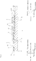
- FIG. 1 An embodiment of the wired circuit board of the present invention is described with reference to FIG. 1 and FIG. 2 .
- a conductor layer 7 (described below) is omitted in FIG. 1 .
- the wired circuit board for battery 1 extends in a surface direction orthogonal to a thickness direction.
- the wired circuit board for battery 1 includes a first portion 2 and a second portion 3 sequentially in the surface direction.
- the shape and dimensions of the first portion 2 are not especially limited.
- the first portion 2 has, for example, an approximately rectangular shape in the plan view.
- the first portion 2 extends in a first direction.
- the first direction is included in the surface direction.
- the second portion 3 continues to the other edge in the first direction of the first portion 2.
- the second portion 3 extends from the other edge in the first direction of the first portion 2 to the other side in the first direction.
- the shape and dimensions of the second portion 3 are not especially limited.
- the second portion 3 has, for example, an approximately circular shape in the plan view.
- the wired circuit board for battery 1 includes a stainless steel layer 5, an insulating base layer 6And the conductor layer 7 sequentially toward one side in the thickness direction. Each of the stainless steel layer 5, insulating base layer 6And conductor layer 7 traverses the first portion 2 and second portion 3.
- the stainless steel layer 5 forms the outermost surface at the other side in the thickness direction of the wired circuit board for battery 1. In other words, the stainless steel layer 5 is exposed toward the other side in the thickness direction.
- the stainless steel layer 5 extends in the surface direction. When being projected in the thickness direction, an outer peripheral edge 4 of the stainless steel layer 5 may correspond to an outer peripheral edge of the wired circuit board for battery 1.
- the stainless steel layer 5 has a thickness of, for example, 5 ⁇ m or more, preferably, 10 ⁇ m or more and, for example, 200 ⁇ m or less, preferably, 100 ⁇ m or less.
- the insulating base layer 6 has a base opening 8 as an exemplary opening penetrating the insulating base layer 6 in the thickness direction.
- the base opening 8 exposes a one-side surface in the thickness direction of the stainless steel layer 5 in the first portion 2.
- the portion of the stainless steel layer 5 exposed from the base opening 8 is the first laser weld portion 22 as an exemplary laser weld portion.
- a one-side surface and the other-side surface in the thickness direction of the first laser weld portion 22 are exposed to one side and the other side in the thickness direction, respectively.
- the first laser weld portion 22 is, for example, 25 mm2 or less, preferably, 10 mm2 or less, more preferably, 1 mm2 or less and, for example, 1 ⁇ m2 or more in area.
- the area is the area of the one-side surface in the thickness direction of the first laser weld portion 22, namely, the exposed area of the first laser weld portion 22.
- the wired circuit board for battery 1 can be downsized.
- an outer peripheral edge 9 of the insulating base layer 6 may correspond to the outer peripheral edge 4 of the stainless steel layer 5 when being projected in the thickness direction.
- the outer peripheral edge 9 of the insulating base layer 6 includes a displaced portion 11.
- the displaced portion 11 When being projected in the thickness direction, the displaced portion 11 is displaced to one side in the second direction with respect to the other-side end in the second direction of the outer peripheral edge 4 of the stainless steel layer 5.
- the second direction is included in the surface direction and orthogonal to the first direction.
- the portion of the stainless steel layer 5 disposed at the other side in the second direction with respect to the displaced portion 11 is the second laser weld portion 23 as an exemplary laser weld portion.
- the second laser weld portion 23 protrudes from the displaced portion 11 of the insulating base layer 6 to the other side in the second direction.
- the second laser weld portion 23 has an approximately arched shape in the plan view (or an approximately crescent shape in the plan view).
- the second laser weld portion 23 has (a maximum value L of) a second direction length, or, (the maximum value of) a protrusion length of, for example, 5 ⁇ m or more, preferably, 10 ⁇ m or more and, for example, 5 mm or less, preferably, 2 mm or less.
- the protrusion length is the above-described upper limit or less
- the wired circuit board for battery 1 can be downsized.
- the protrusion length is the above-described lower limit or more
- the second laser weld portion 23 can surely be laser welded. Thus, a battery module 20 with excellent reliability can be produced.
- the insulating base layer 6 further has a second opening 13 and a third opening 14. Each of the second opening 13 and third opening 14 penetrates the insulating base layer 6 in the thickness direction.
- Examples of the material of the insulating base layer 6 include resin.
- Examples of the resin include polyimide.
- the insulating base layer 6 has a thickness of, for example, 1 ⁇ m or more and, for example, 50 ⁇ m or less.
- the conductor layer 7 traverses the first portion 2 and second portion 3.
- the conductor layer 7 is disposed on a one-side surface in the thickness direction of the insulating base layer 6.
- the conductor layer 7 includes a conductor pattern 15.
- the conductor pattern 15 includes a first connection portion 17, a second connection portion 18, and a terminal 19.
- the second opening 13 is filled with the first connection portion 17.
- the other-side surface in the thickness direction of the first connection portion 17 is in contact with the one-side surface in the thickness direction of the stainless steel layer 5.
- the third opening 14 is filled with the second connection portion 18.
- the other-side surface in the thickness direction of the second connection portion 18 is in contact with the one-side surface in the thickness direction of the stainless steel layer 5.
- the terminal 19 is electrically connected to the stainless steel layer 5 via the first connection portion 17 and second connection portion 18.
- Examples of the material of the conductor layer 7 include a conductor.
- Examples of the conductor include copper.
- the conductor layer 7 has a thickness of, for example, 1 ⁇ m or more and, for example, 50 ⁇ m or less. The thickness of the conductor layer 7 is a distance between the one-side surface in the thickness direction of the insulating base layer 6And a one-side surface in the thickness direction of the conductor layer 7.
- a method of producing the wired circuit board for battery 1 is described. First, the stainless steel layer 5 is prepared. Next, the insulating base layer 6 is disposed. For example, varnish including resin is applied and dried, thereby forming the insulating base layer 6. Thereafter, the conductor layer 7 is disposed. For example, by an additive method or a subtractive method, the conductor layer 7 is formed. In this manner, the wired circuit board for battery 1 is produced.
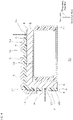
- the wired circuit board for battery 1 is, for example, as illustrated in FIG. 3 and FIG. 4 , included in the battery module 20.
- the battery module 20 includes a battery 21 and the wired circuit board for battery 1.
- the battery 21 has an approximately cylindrical shape.
- the battery 21 has a flat shape.
- the axis-direction length of the battery 21 is, for example, shorter than its diameter.
- the battery 21 has a button shape.
- Examples of the battery 21 include a primary battery, and a secondary battery.
- the battery 21 has a one-side surface and the other-side surface in the thickness direction, and a peripheral surface connecting a peripheral edge of the one-side surface and a peripheral edge of the other-side surface.
- the battery 21 includes a negative terminal 25 as an exemplary electrode and a positive terminal 26As an exemplary electrode.
- the negative terminal 25 forms the one-side surface in the thickness direction of the battery 21.
- the above-described second laser weld portion 23 of the wired circuit board for battery 1 is laser welded to the negative terminal 25.
- the positive terminal 26 forms at least a side surface (specifically, the side surface and the other-side surface) of the battery 21.
- the first laser weld portion 22 of the above-described wired circuit board for battery 1 is laser welded to the positive terminal 26.
- a method of producing the battery module 20 is described. First, the battery 21 and wired circuit board for battery 1 are prepared. Next, the wired circuit board for battery 1 is folded so that the boundary between the first portion 2 and second portion 3 forms a valley (folded portion). The stainless steel layer 5 on the first portion 2 and the stainless steel layer 5 on the second portion 3 of the folded wired circuit board for battery 1 are brought into contact with the positive terminal 26And negative terminal 25, respectively.
- first laser weld portion 22 and second laser weld portion 23 are irradiated with a laser beam to weld the first laser weld portion 22 to the positive terminal 26And the second laser weld portion 23 to the negative terminal 25, respectively.
- a laser beam is delivered from a lateral side of the battery module 20 to the first laser weld portion 22. Meanwhile, a laser beam is delivered from the one side in the thickness direction of the battery module 20 to the second laser weld portion 23.
- the conditions for the laser irradiation are not especially limited.
- the battery module 20 is used for, for example, a wireless power transmission device, or a wearable device.
- the wireless power transmission device include a small device.
- Specific examples of the small device include a hearing aid.
- the wired circuit board for battery 1 includes the first laser weld portion 22 and second laser weld portion 23, and can be laser welded to the negative terminal 25 and positive terminal 26 of the battery 21 with the first laser weld portion 22 and second laser weld portion 23.
- the battery module 20 does not include a metal plate as described Patent Document 1. Thus, the battery module 20 including the wired circuit board for battery 1 can be downsized.
- the second laser weld portion 23 protrudes from the outer peripheral edge 9 of the insulating base layer 6 to the other side in the second direction. Thus, a step of exposing the second laser weld portion 23 is not needed. Therefore, the second laser weld portion 23 can directly be welded.
- the wired circuit board for battery 1 can be downsized.
- the second laser weld portion 23 can surely be laser welded. Thus, a battery module with excellent reliability can be produced.
- the first laser weld portion 22 is exposed from the base opening 8. Thus, a step of exposing the first laser weld portion 22 is not needed. Therefore, the first laser weld portion 22 can directly be welded.
- the wired circuit board for battery 1 can be downsized.
- the battery module 20 including the small wired circuit board for battery 1 is downsized.
- the first portion 2 includes the first laser weld portion 22, and the second portion 3 includes the second laser weld portion 23.
- a second portion 3 includes a first laser weld portion 22.
- a first portion 2 includes a second laser weld portion 23.
- the first portion 2 can include the first laser weld portion 22 and second laser weld portion 23.
- the second portion 3 can include the first laser weld portion 22 and second laser weld portion 23.
- a stainless steel layer 5 can include one of the first laser weld portion 22 and second laser weld portion 23.
- the stainless steel layer 5 can have an island. On the stainless steel layer 5, the island is separated from its peripheral portions with a space, and insulated. The island overlaps a second opening 13 or a third opening 14 of an insulating base layer 6.
- the wired circuit board for battery 1 may include a cover insulating layer covering a conductor pattern 15.
- the stainless steel layer 5 electrically connected to a first connection portion 17 may be laser welded to a negative terminal 25.
- the stainless steel layer 5 electrically connected to a second connection portion 18 may be laser welded to a positive terminal 26Both of the stainless steel layer 5 electrically connected to the first connection portion 17 and stainless steel layer 5 electrically connected to the second connection portion 18 may be laser welded to the stainless steel layer 5 or to the positive terminal 26.
- the wired circuit board for battery 1 may include only one of the first portion 2 and second portion 3.
- a stainless steel layer 5 and an insulating base layer 6 include a slit 56.
- the insulating base layer 6 is omitted.
- the slit 56 is disposed around the base opening 8. The slit 56 penetrates the stainless steel layer 5 and the insulating base layer 6 in the thickness direction.
- This variation demonstrates that the slit 56 has an approximately arc shape.
- a plurality (four) of the slits 56 is disposed with a space therebetween in a circumferential direction of the base opening 8.
- the plurality of slits 56 intermittently forms an approximately ringed shape in the circumferential direction.
- the ratio of the area of the slits 56 to the opening area of the base opening 8 is, for example, 0.1 or more and, for example, 0.9 or less.
- the first portion 2 includes a plurality (two) of the first laser weld portions 22 (the base openings 8, see FIG. 6B ).
- the first laser weld portions 22 are arranged in the second direction.
- the first laser weld portions 22 are separated with a space therebetween in the second direction.
- Each of the first laser weld portions 22 is provided with the above-described plurality (four) of slits 56.
- the stainless steel layer 5 and the insulating base layer 6 include the slits 56.
- the deformation includes, for example, a crease.
- a slit 56 has an approximately straight line shape in the plan view.
- the slits 56 extend in the first direction.
- the slits 56 are separated with a space therebetween in the second direction.
- a base opening 8 is surrounded by the slits 56. This variation demonstrates that two base openings 8 are provided among three slits 56.
- a stainless steel layer 5 includes a slit 56 in a first portion 2.
- An insulating base layer 6 does not include a slit 56.
- a plurality of slits 56 define the second laser weld portion 23.
- the second laser weld portion 23 is disposed inside a plurality of slits 56.
- the plurality of slits 56 intermittently forms an approximately ringed shape in the circumferential direction.
- the region of the second laser weld portion 23 is a region surrounded by the plurality of slits 56.
- the ratio of the area of the slits 56 to the area of the second laser weld portion 23 is, for example, 0.1 or more and, for example, 0.9 or less.
- the first portion 2 includes a plurality (two) of second laser weld portions 23.
- the second laser weld portions 23 are arranged in the second direction.
- the second laser weld portions 23 are separated with a space therebetween in the second direction.
- Each of the second laser weld portions 23 is provided with the plurality (four) of slits 56.
- the stainless steel layer 5 includes the slits 56.
- the deformation includes, for example, a crease.
- the second laser weld portions 23 are surrounded by a plurality of slits 56 having an approximately straight line shape in the plan view. While the illustrative embodiments of the present invention are provided in the above description, such is for illustrative purpose only and it is not to be construed as limiting in any manner. Modification and variation of the present invention that will be obvious to those skilled in the art is to be covered by the following claims.
Landscapes
- Engineering & Computer Science (AREA)
- Chemical & Material Sciences (AREA)
- Chemical Kinetics & Catalysis (AREA)
- Electrochemistry (AREA)
- General Chemical & Material Sciences (AREA)
- Microelectronics & Electronic Packaging (AREA)
- Manufacturing & Machinery (AREA)
- Battery Mounting, Suspending (AREA)
- Connection Of Batteries Or Terminals (AREA)
Abstract
A wired circuit board for battery 1 includes a stainless steel layer 5, an insulating base layer 6, and a conductor layer 7 sequentially toward one side in the thickness direction. The stainless steel layer 5 is electrically connected to the conductor layer 7. The stainless steel layer 5 includes a first laser weld portion 22 that can be laser welded. The first laser weld portion 22 is exposed to the one side and the other side in the thickness direction.
Description
- The present invention relates to a wired circuit board for battery and a battery module.
- Battery modules including a battery, a metal plate, and a printed circuit board sequentially in its thickness direction have been known (for example, see
Patent Document 1 cited below). In the battery module described inPatent Document 1, the metal plate is welded, thereby fixing and connecting the printed circuit board to the battery. - Patent Document 1:
Japanese Unexamined Patent Publication No. 2002-329491 - There is a need for downsized battery modules. However, a battery module as described in
Patent Document 1 includes a metal plate. Thus, there is a disadvantage that such a module battery cannot meet the above-mentioned need. - The present invention provides a downsized battery module and a wired circuit board for battery included therein.
- The present invention [1] includes a wired circuit board for battery comprising: a stainless steel layer; an insulating base layer; and a conductor layer sequentially toward one side in a thickness direction, wherein the stainless steel layer is electrically connected to the conductor layer, the stainless steel layer includes a laser weld portion that can be laser welded, and the laser weld portion is exposed to the one side and the other side in the thickness direction..
- The wired circuit board for battery includes the laser weld portion and thus can be laser welded to the battery module with the laser weld portion. In other words, the wired circuit board for battery does not include a metal plate as described in
Patent Document 1. Therefore, the battery module including the wired circuit board for battery can be downsized. - The present invention [2] includes the wired circuit board for battery described in [1] above, wherein the insulating base layer includes an outer peripheral edge, and the laser weld portion protrudes outward from the outer peripheral edge in a direction orthogonal to the thickness direction.
- In the wired circuit board for battery, the laser weld portion protrudes outward from the outer peripheral edge. Thus, a step of exposing the laser weld portion is not needed, and the laser weld portion can directly be laser welded.
- The present invention [3] includes the wired circuit board for battery described in [2] above, wherein the laser weld portion has a protrusion length of 5 µm or more and 5 mm or less.
- The wired circuit board for battery has a protrusion length of 5 mm or less. Thus, the wired circuit board for battery can be downsized. In the wired circuit board for battery, the protrusion length is 5 µm or more. Thus, the laser weld portion can surely be laser welded. Therefore, a battery module excellent in reliability can be produced.
- The present invention [4] includes the wired circuit board for battery described in [2] or [3] above, wherein the stainless steel layer has a slit around the laser weld portion.
- In the wired circuit board for battery, the stainless steel layer and the insulating base layer include the slit. Thus, when the laser weld portion is laser welded, deformation of the stainless steel layer and insulating base layer by the heat of the laser welding can be suppressed.
- The present invention [5] includes the wired circuit board for battery described in [1] above, wherein the insulating base layer has an opening penetrating the insulating base layer in the thickness direction, and the laser weld portion is exposed from the opening to the one side in the thickness direction.
- In the wired circuit board for battery, the laser weld portion is exposed from the opening. Thus, a step of exposing the laser weld portion is not needed, and the laser weld portion can directly be laser welded.
- The present invention [6] includes the wired circuit board for battery described in [5] above, wherein the laser weld portion has an exposed area of 25 mm2 or less.
- In the wired circuit board for battery, the laser weld portion has an exposed area of 25 mm2 or less. Thus, the wired circuit board for battery can be downsized.
- The present invention [7] includes the wired circuit board for battery described in [5] or [6] above, wherein the stainless steel layer and the insulating base layer have a slit disposed around the opening.
- In the wired circuit board for battery, the stainless steel layer includes the slit. Thus, when the laser weld portion is laser welded, deformation of the stainless steel layer by the heat of the laser welding can be suppressed.
- The present invention [8] includes a battery module comprising: the wired circuit board for battery described in any one of [1] to [7] above; and a battery including an electrode welded to the laser weld portion.
- The battery module is downsized because including the above-described wired circuit board for battery.
- The battery module including the wired circuit board for battery of the present invention is downsized.
-
- [
FIG. 1] FIG. 1 is a plan view of an embodiment of the wired circuit board for battery of the present invention. - [
FIG. 2] FIG. 2 is a cross-sectional view taken along line X-X of the wired circuit board for battery illustrated inFIG. 1 . - [
FIG. 3] FIG. 3 is a perspective view of the battery module including the wired circuit board for battery illustrated inFIG. 1 andFIG. 2 . - [
FIG. 4] FIG. 4 is a cross-sectional view of the battery module along the dotted line ofFIG. 3 . - [
FIG. 5] FIG. 5 is a plan view of a variation of the wired circuit board for battery illustrated inFIG. 1 . - [
FIG. 6] FIG. 6A and FIG. 6B are enlarged views of the first laser weld portion of the wired circuit board for battery of a variation.FIG. 6A is a plan view thereof.FIG. 6B is a cross-sectional view taken along line X-X ofFIG. 6A . - [
FIG. 7] FIG. 7A and FIG. 7B are enlarged views of the first laser weld portion of the wired circuit board for battery of a variation.FIG. 7A is a plan view thereof.FIG. 7B is a cross-sectional view taken along line Y-Y ofFIG. 7A . - [
FIG. 8] FIG. 8A and FIG. 8B are enlarged views of the second laser weld portion of the wired circuit board for battery of a variation.FIG. 8A is a plan view thereof.FIG. 8B is a cross-sectional view taken along line X-X ofFIG. 8A . - [
FIG. 9] FIG. 9A and FIG. 9B are enlarged views of the second laser weld portion of the wired circuit board for battery of a variation.FIG. 9A is a plan view thereof.FIG. 9B is a cross-sectional view taken along line Y-Y ofFIG. 9A . - An embodiment of the wired circuit board of the present invention is described with reference to
FIG. 1 andFIG. 2 . To clarify the shapes and dispositions of a firstlaser weld portion 22 and a second laser weld portion 23 (both described below) in a wired circuit board for battery 1 (described below), a conductor layer 7 (described below) is omitted inFIG. 1 . - The wired circuit board for
battery 1 extends in a surface direction orthogonal to a thickness direction. The wired circuit board forbattery 1 includes afirst portion 2 and asecond portion 3 sequentially in the surface direction. - The shape and dimensions of the
first portion 2 are not especially limited. Thefirst portion 2 has, for example, an approximately rectangular shape in the plan view. Thefirst portion 2 extends in a first direction. The first direction is included in the surface direction. - The
second portion 3 continues to the other edge in the first direction of thefirst portion 2. Thesecond portion 3 extends from the other edge in the first direction of thefirst portion 2 to the other side in the first direction. The shape and dimensions of thesecond portion 3 are not especially limited. Thesecond portion 3 has, for example, an approximately circular shape in the plan view. - The wired circuit board for
battery 1 includes astainless steel layer 5, an insulating base layer 6And theconductor layer 7 sequentially toward one side in the thickness direction. Each of thestainless steel layer 5, insulating base layer 6Andconductor layer 7 traverses thefirst portion 2 andsecond portion 3. - The
stainless steel layer 5 forms the outermost surface at the other side in the thickness direction of the wired circuit board forbattery 1. In other words, thestainless steel layer 5 is exposed toward the other side in the thickness direction. Thestainless steel layer 5 extends in the surface direction. When being projected in the thickness direction, an outerperipheral edge 4 of thestainless steel layer 5 may correspond to an outer peripheral edge of the wired circuit board forbattery 1. Thestainless steel layer 5 has a thickness of, for example, 5 µm or more, preferably, 10 µm or more and, for example, 200 µm or less, preferably, 100 µm or less. - In the
first portion 2, the insulatingbase layer 6 has abase opening 8 as an exemplary opening penetrating the insulatingbase layer 6 in the thickness direction. Thebase opening 8 exposes a one-side surface in the thickness direction of thestainless steel layer 5 in thefirst portion 2. The portion of thestainless steel layer 5 exposed from thebase opening 8 is the firstlaser weld portion 22 as an exemplary laser weld portion. A one-side surface and the other-side surface in the thickness direction of the firstlaser weld portion 22 are exposed to one side and the other side in the thickness direction, respectively. The firstlaser weld portion 22 is, for example, 25 mm2 or less, preferably, 10 mm2 or less, more preferably, 1 mm2 or less and, for example, 1 µm2 or more in area. The area is the area of the one-side surface in the thickness direction of the firstlaser weld portion 22, namely, the exposed area of the firstlaser weld portion 22. When the area is the above-described upper limit or less, the wired circuit board forbattery 1 can be downsized. In thefirst portion 2, an outerperipheral edge 9 of the insulatingbase layer 6 may correspond to the outerperipheral edge 4 of thestainless steel layer 5 when being projected in the thickness direction. - In the
second portion 3, the outerperipheral edge 9 of the insulatingbase layer 6 includes a displacedportion 11. When being projected in the thickness direction, the displacedportion 11 is displaced to one side in the second direction with respect to the other-side end in the second direction of the outerperipheral edge 4 of thestainless steel layer 5. The second direction is included in the surface direction and orthogonal to the first direction. The portion of thestainless steel layer 5 disposed at the other side in the second direction with respect to the displaced portion 11 (an example of the outside) is the secondlaser weld portion 23 as an exemplary laser weld portion. The secondlaser weld portion 23 protrudes from the displacedportion 11 of the insulatingbase layer 6 to the other side in the second direction. In the present embodiment, the secondlaser weld portion 23 has an approximately arched shape in the plan view (or an approximately crescent shape in the plan view). - The second
laser weld portion 23 has (a maximum value L of) a second direction length, or, (the maximum value of) a protrusion length of, for example, 5 µm or more, preferably, 10 µm or more and, for example, 5 mm or less, preferably, 2 mm or less. When the protrusion length is the above-described upper limit or less, the wired circuit board forbattery 1 can be downsized. When the protrusion length is the above-described lower limit or more, the secondlaser weld portion 23 can surely be laser welded. Thus, abattery module 20 with excellent reliability can be produced. - As illustrated in
FIG. 2 , the insulatingbase layer 6 further has asecond opening 13 and athird opening 14. Each of thesecond opening 13 andthird opening 14 penetrates the insulatingbase layer 6 in the thickness direction. - Examples of the material of the insulating
base layer 6 include resin. Examples of the resin include polyimide. The insulatingbase layer 6 has a thickness of, for example, 1 µm or more and, for example, 50 µm or less. - The
conductor layer 7 traverses thefirst portion 2 andsecond portion 3. Theconductor layer 7 is disposed on a one-side surface in the thickness direction of the insulatingbase layer 6. Theconductor layer 7 includes aconductor pattern 15. Theconductor pattern 15 includes afirst connection portion 17, asecond connection portion 18, and a terminal 19. Thesecond opening 13 is filled with thefirst connection portion 17. The other-side surface in the thickness direction of thefirst connection portion 17 is in contact with the one-side surface in the thickness direction of thestainless steel layer 5. Thethird opening 14 is filled with thesecond connection portion 18. The other-side surface in the thickness direction of thesecond connection portion 18 is in contact with the one-side surface in the thickness direction of thestainless steel layer 5. The terminal 19 is electrically connected to thestainless steel layer 5 via thefirst connection portion 17 andsecond connection portion 18. Examples of the material of theconductor layer 7 include a conductor. Examples of the conductor include copper. Theconductor layer 7 has a thickness of, for example, 1 µm or more and, for example, 50 µm or less. The thickness of theconductor layer 7 is a distance between the one-side surface in the thickness direction of the insulating base layer 6And a one-side surface in the thickness direction of theconductor layer 7. - A method of producing the wired circuit board for
battery 1 is described. First, thestainless steel layer 5 is prepared. Next, the insulatingbase layer 6 is disposed. For example, varnish including resin is applied and dried, thereby forming the insulatingbase layer 6. Thereafter, theconductor layer 7 is disposed. For example, by an additive method or a subtractive method, theconductor layer 7 is formed. In this manner, the wired circuit board forbattery 1 is produced. - The wired circuit board for
battery 1 is, for example, as illustrated inFIG. 3 andFIG. 4 , included in thebattery module 20. Thebattery module 20 includes abattery 21 and the wired circuit board forbattery 1. - The
battery 21 has an approximately cylindrical shape. Thebattery 21 has a flat shape. The axis-direction length of thebattery 21 is, for example, shorter than its diameter. In short, thebattery 21 has a button shape. Examples of thebattery 21 include a primary battery, and a secondary battery. Thebattery 21 has a one-side surface and the other-side surface in the thickness direction, and a peripheral surface connecting a peripheral edge of the one-side surface and a peripheral edge of the other-side surface. Thebattery 21 includes anegative terminal 25 as an exemplary electrode and a positive terminal 26As an exemplary electrode. - The negative terminal 25 forms the one-side surface in the thickness direction of the
battery 21. The above-described secondlaser weld portion 23 of the wired circuit board forbattery 1 is laser welded to thenegative terminal 25. - The positive terminal 26 forms at least a side surface (specifically, the side surface and the other-side surface) of the
battery 21. The firstlaser weld portion 22 of the above-described wired circuit board forbattery 1 is laser welded to thepositive terminal 26. - A method of producing the
battery module 20 is described. First, thebattery 21 and wired circuit board forbattery 1 are prepared. Next, the wired circuit board forbattery 1 is folded so that the boundary between thefirst portion 2 andsecond portion 3 forms a valley (folded portion). Thestainless steel layer 5 on thefirst portion 2 and thestainless steel layer 5 on thesecond portion 3 of the folded wired circuit board forbattery 1 are brought into contact with the positive terminal 26Andnegative terminal 25, respectively. - Thereafter, the first
laser weld portion 22 and secondlaser weld portion 23 are irradiated with a laser beam to weld the firstlaser weld portion 22 to the positive terminal 26And the secondlaser weld portion 23 to thenegative terminal 25, respectively. - Specifically, a laser beam is delivered from a lateral side of the
battery module 20 to the firstlaser weld portion 22. Meanwhile, a laser beam is delivered from the one side in the thickness direction of thebattery module 20 to the secondlaser weld portion 23. The conditions for the laser irradiation are not especially limited. - The
battery module 20 is used for, for example, a wireless power transmission device, or a wearable device. Examples of the wireless power transmission device include a small device. Specific examples of the small device include a hearing aid. - The wired circuit board for
battery 1 includes the firstlaser weld portion 22 and secondlaser weld portion 23, and can be laser welded to thenegative terminal 25 andpositive terminal 26 of thebattery 21 with the firstlaser weld portion 22 and secondlaser weld portion 23. Thebattery module 20 does not include a metal plate as describedPatent Document 1. Thus, thebattery module 20 including the wired circuit board forbattery 1 can be downsized. - In the wired circuit board for
battery 1, the secondlaser weld portion 23 protrudes from the outerperipheral edge 9 of the insulatingbase layer 6 to the other side in the second direction. Thus, a step of exposing the secondlaser weld portion 23 is not needed. Therefore, the secondlaser weld portion 23 can directly be welded. - When (the maximum value of) the protrusion length of the second
laser weld portion 23 is 5 mm or less, the wired circuit board forbattery 1 can be downsized. When (the maximum value of) the protrusion length of the secondlaser weld portion 23 is 5 µm or more, the secondlaser weld portion 23 can surely be laser welded. Thus, a battery module with excellent reliability can be produced. - Similarly, in the wired circuit board for
battery 1, the firstlaser weld portion 22 is exposed from thebase opening 8. Thus, a step of exposing the firstlaser weld portion 22 is not needed. Therefore, the firstlaser weld portion 22 can directly be welded. - When the exposed area of the first
laser weld portion 22 is 25 mm2 or less, the wired circuit board forbattery 1 can be downsized. - The
battery module 20 including the small wired circuit board forbattery 1 is downsized. - In the following variation, the same members and steps as in the above-described embodiment are given the same numerical references and the detailed descriptions thereof are omitted. Further, the variation has the same operations and effects as those of the embodiment unless especially described otherwise. Furthermore, the embodiment and variation can appropriately be combined.
- In the embodiment, the
first portion 2 includes the firstlaser weld portion 22, and thesecond portion 3 includes the secondlaser weld portion 23. In the variation, as illustrated inFIG. 5 , asecond portion 3 includes a firstlaser weld portion 22. Afirst portion 2 includes a secondlaser weld portion 23. Although not illustrated, thefirst portion 2 can include the firstlaser weld portion 22 and secondlaser weld portion 23. Although not illustrated, thesecond portion 3 can include the firstlaser weld portion 22 and secondlaser weld portion 23. - A
stainless steel layer 5 can include one of the firstlaser weld portion 22 and secondlaser weld portion 23. - Although not illustrated, the
stainless steel layer 5 can have an island. On thestainless steel layer 5, the island is separated from its peripheral portions with a space, and insulated. The island overlaps asecond opening 13 or athird opening 14 of aninsulating base layer 6. - Although not illustrated, the wired circuit board for
battery 1 may include a cover insulating layer covering aconductor pattern 15. - Although not illustrated, the
stainless steel layer 5 electrically connected to afirst connection portion 17 may be laser welded to anegative terminal 25. Thestainless steel layer 5 electrically connected to asecond connection portion 18 may be laser welded to a positive terminal 26Both of thestainless steel layer 5 electrically connected to thefirst connection portion 17 andstainless steel layer 5 electrically connected to thesecond connection portion 18 may be laser welded to thestainless steel layer 5 or to thepositive terminal 26. - Although not illustrated, the wired circuit board for
battery 1 may include only one of thefirst portion 2 andsecond portion 3. - As illustrated in
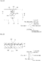
FIG. 6A and FIG. 6B , this variation demonstrates that astainless steel layer 5 and an insulating base layer 6 (seeFIG. 6B ) include aslit 56. InFIG. 6A , the insulatingbase layer 6 is omitted. As illustrated inFIG. 6B , theslit 56 is disposed around thebase opening 8. Theslit 56 penetrates thestainless steel layer 5 and the insulatingbase layer 6 in the thickness direction. This variation demonstrates that theslit 56 has an approximately arc shape. A plurality (four) of theslits 56 is disposed with a space therebetween in a circumferential direction of thebase opening 8. The plurality ofslits 56 intermittently forms an approximately ringed shape in the circumferential direction. The ratio of the area of theslits 56 to the opening area of the base opening 8 (the area of the first laser weld portion 22) is, for example, 0.1 or more and, for example, 0.9 or less. - The
first portion 2 includes a plurality (two) of the first laser weld portions 22 (thebase openings 8, seeFIG. 6B ). The firstlaser weld portions 22 are arranged in the second direction. The firstlaser weld portions 22 are separated with a space therebetween in the second direction. Each of the firstlaser weld portions 22 is provided with the above-described plurality (four) ofslits 56. - In the variation illustrated in
FIG. 6A and FIG. 6B , thestainless steel layer 5 and the insulatingbase layer 6 include theslits 56. Thus, when the firstlaser weld portions 22 are laser welded, deformation of thestainless steel layer 5 and insulatingbase layer 6 by the heat of the laser welding can be suppressed. The deformation includes, for example, a crease. - In the variation illustrated in
FIG. 7A and FIG. 7B , aslit 56 has an approximately straight line shape in the plan view. Theslits 56 extend in the first direction. Theslits 56 are separated with a space therebetween in the second direction. - As illustrated in
FIG. 7B , abase opening 8 is surrounded by theslits 56. This variation demonstrates that twobase openings 8 are provided among threeslits 56. - As illustrated in
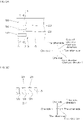
FIG. 8A and FIG. 8B , this variation demonstrates that astainless steel layer 5 includes aslit 56 in afirst portion 2. Aninsulating base layer 6 does not include aslit 56. As illustrated inFIG. 8B , a plurality ofslits 56 define the secondlaser weld portion 23. The secondlaser weld portion 23 is disposed inside a plurality ofslits 56. The plurality ofslits 56 intermittently forms an approximately ringed shape in the circumferential direction. The region of the secondlaser weld portion 23 is a region surrounded by the plurality ofslits 56. The ratio of the area of theslits 56 to the area of the secondlaser weld portion 23 is, for example, 0.1 or more and, for example, 0.9 or less. - The
first portion 2 includes a plurality (two) of secondlaser weld portions 23. The secondlaser weld portions 23 are arranged in the second direction. The secondlaser weld portions 23 are separated with a space therebetween in the second direction. Each of the secondlaser weld portions 23 is provided with the plurality (four) ofslits 56. - In the variation illustrated in
FIG. 8A and FIG. 8B , thestainless steel layer 5 includes theslits 56. Thus, when the secondlaser weld portions 23 are laser welded, deformation of thestainless steel layer 5 by the heat of the laser welding can be suppressed. The deformation includes, for example, a crease. - As illustrated in
FIG. 9A and FIG. 9B , the secondlaser weld portions 23 are surrounded by a plurality ofslits 56 having an approximately straight line shape in the plan view. While the illustrative embodiments of the present invention are provided in the above description, such is for illustrative purpose only and it is not to be construed as limiting in any manner. Modification and variation of the present invention that will be obvious to those skilled in the art is to be covered by the following claims. - 1
- wired circuit board for battery
- 4
- outer peripheral edge
- 5
- stainless steel layer
- 6
- insulating base layer
- 8
- base opening
- 7
- conductor layer
- 9
- outer peripheral edge
- 19
- terminal
- 20
- battery module
- 21
- battery
- 56
- slit
Claims (8)
- A wired circuit board for battery comprising:
a stainless steel layer; an insulating base layer; and a conductor layer sequentially toward one side in a thickness direction,wherein the stainless steel layer is electrically connected to the conductor layer,the stainless steel layer includes a laser weld portion that can be laser welded, andthe laser weld portion is exposed to the one side and the other side in the thickness direction. - The wired circuit board for battery according to Claim 1, wherein the insulating base layer includes an outer peripheral edge, and
the laser weld portion protrudes outward from the outer peripheral edge in a direction orthogonal to the thickness direction. - The wired circuit board for battery according to Claim 2, wherein the laser weld portion has a protrusion length of 5 µm or more and 5 mm or less.
- The wired circuit board for battery according to Claim 2 or 3, wherein the stainless steel layer has a slit disposed around the laser weld portion.
- The wired circuit board for battery according to Claim 1, wherein the insulating base layer has an opening penetrating the insulating base layer in the thickness direction, and
the laser weld portion is exposed from the opening to the one side in the thickness direction. - The wired circuit board for battery according to Claim 5, wherein the laser weld portion has an exposed area of 25 mm2 or less.
- The wired circuit board for battery according to Claim 5 or 6, wherein the stainless steel layer and the insulating base layer have a slit disposed around the opening.
- A battery module comprising:the wired circuit board for battery according to any one of Claims 1 to 7; anda battery including an electrode welded to the laser weld portion.
Applications Claiming Priority (2)
| Application Number | Priority Date | Filing Date | Title |
|---|---|---|---|
| JP2020200452 | 2020-12-02 | ||
| JP2021182750A JP2022088321A (en) | 2020-12-02 | 2021-11-09 | Battery wiring circuit board and battery module |
Publications (1)
| Publication Number | Publication Date |
|---|---|
| EP4009431A1 true EP4009431A1 (en) | 2022-06-08 |
Family
ID=78770457
Family Applications (1)
| Application Number | Title | Priority Date | Filing Date |
|---|---|---|---|
| EP21209868.5A Withdrawn EP4009431A1 (en) | 2020-12-02 | 2021-11-23 | Wired circuit board for battery and battery module |
Country Status (3)
| Country | Link |
|---|---|
| US (1) | US20220173442A1 (en) |
| EP (1) | EP4009431A1 (en) |
| CN (1) | CN114599147A (en) |
Families Citing this family (1)
| Publication number | Priority date | Publication date | Assignee | Title |
|---|---|---|---|---|
| CN118156736B (en) * | 2024-05-09 | 2024-07-09 | 蜂巢能源科技股份有限公司 | Battery monomer and battery pack |
Citations (5)
| Publication number | Priority date | Publication date | Assignee | Title |
|---|---|---|---|---|
| JP2002329491A (en) | 2001-04-27 | 2002-11-15 | Sanyo Electric Co Ltd | Terminal-attached battery |
| US20060127752A1 (en) * | 2004-12-09 | 2006-06-15 | Trw Automotive U.S. Llc | Battery with printed circuit |
| JP2012142170A (en) * | 2010-12-28 | 2012-07-26 | Hitachi Maxell Energy Ltd | Battery unit |
| EP2704231A1 (en) * | 2011-04-27 | 2014-03-05 | Hitachi Maxell, Ltd. | Battery unit |
| JP2018174123A (en) * | 2017-03-31 | 2018-11-08 | 日東電工株式会社 | Battery pack, wireless power transmission system and hearing aid |
-
2021
- 2021-11-23 EP EP21209868.5A patent/EP4009431A1/en not_active Withdrawn
- 2021-11-24 US US17/534,997 patent/US20220173442A1/en not_active Abandoned
- 2021-12-01 CN CN202111453107.8A patent/CN114599147A/en active Pending
Patent Citations (5)
| Publication number | Priority date | Publication date | Assignee | Title |
|---|---|---|---|---|
| JP2002329491A (en) | 2001-04-27 | 2002-11-15 | Sanyo Electric Co Ltd | Terminal-attached battery |
| US20060127752A1 (en) * | 2004-12-09 | 2006-06-15 | Trw Automotive U.S. Llc | Battery with printed circuit |
| JP2012142170A (en) * | 2010-12-28 | 2012-07-26 | Hitachi Maxell Energy Ltd | Battery unit |
| EP2704231A1 (en) * | 2011-04-27 | 2014-03-05 | Hitachi Maxell, Ltd. | Battery unit |
| JP2018174123A (en) * | 2017-03-31 | 2018-11-08 | 日東電工株式会社 | Battery pack, wireless power transmission system and hearing aid |
Also Published As
| Publication number | Publication date |
|---|---|
| US20220173442A1 (en) | 2022-06-02 |
| CN114599147A (en) | 2022-06-07 |
Similar Documents
| Publication | Publication Date | Title |
|---|---|---|
| CN109690857B (en) | Stacked electrode assembly and flexible rechargeable battery including the same | |
| JP2022540192A (en) | Electrode assembly and battery | |
| EP4009431A1 (en) | Wired circuit board for battery and battery module | |
| EP0662699A1 (en) | A helical induction coil, a device for forming and a method of making same | |
| JP2013114950A (en) | Connector | |
| JP2008270420A (en) | Wiring circuit board and fuel cell | |
| CN110226244A (en) | Secondary battery | |
| CN118249048A (en) | Current collectors, top cover components, batteries and electrical equipment | |
| KR20230018464A (en) | Battery assembly and medical capsule | |
| JP2010140875A (en) | Shield wire and terminal shield structure of shield wire | |
| US20230009006A1 (en) | Wiring circuit board and method for manufacturing same | |
| CN111971766A (en) | Capacitor and method for producing a capacitor | |
| JP2022088321A (en) | Battery wiring circuit board and battery module | |
| US20210408649A1 (en) | Rechargeable battery | |
| JP2010049859A (en) | Shield connector | |
| US4486810A (en) | Electrode lead tab for capacitor | |
| US10225926B2 (en) | Contact arrangement for a multi-layer circuit board | |
| JPH0927363A (en) | Connector structure for multilayered printed circuit board | |
| EP4170784A1 (en) | Rechargeable battery | |
| WO2021257358A1 (en) | Surface-mount-assembly z-shaped pin | |
| JPH04137380A (en) | Connecting device of crimp-style terminal | |
| US12063738B2 (en) | Multilayer substrate and method for manufacturing same | |
| EP4007056A1 (en) | Battery module and battery module with wired circuit board | |
| US20240244756A1 (en) | Assembly sheet | |
| US20230380058A1 (en) | Wiring circuit board |
Legal Events
| Date | Code | Title | Description |
|---|---|---|---|
| PUAI | Public reference made under article 153(3) epc to a published international application that has entered the european phase |
Free format text: ORIGINAL CODE: 0009012 |
|
| STAA | Information on the status of an ep patent application or granted ep patent |
Free format text: STATUS: THE APPLICATION HAS BEEN PUBLISHED |
|
| AK | Designated contracting states |
Kind code of ref document: A1 Designated state(s): AL AT BE BG CH CY CZ DE DK EE ES FI FR GB GR HR HU IE IS IT LI LT LU LV MC MK MT NL NO PL PT RO RS SE SI SK SM TR |
|
| STAA | Information on the status of an ep patent application or granted ep patent |
Free format text: STATUS: THE APPLICATION IS DEEMED TO BE WITHDRAWN |
|
| 18D | Application deemed to be withdrawn |
Effective date: 20221209 |