EP4009390A1 - Display apparatus - Google Patents
Display apparatus Download PDFInfo
- Publication number
- EP4009390A1 EP4009390A1 EP21218491.5A EP21218491A EP4009390A1 EP 4009390 A1 EP4009390 A1 EP 4009390A1 EP 21218491 A EP21218491 A EP 21218491A EP 4009390 A1 EP4009390 A1 EP 4009390A1
- Authority
- EP
- European Patent Office
- Prior art keywords
- area
- layer
- protective film
- display apparatus
- substrate
- Prior art date
- Legal status (The legal status is an assumption and is not a legal conclusion. Google has not performed a legal analysis and makes no representation as to the accuracy of the status listed.)
- Withdrawn
Links
Images


Classifications
-
- G—PHYSICS
- G09—EDUCATION; CRYPTOGRAPHY; DISPLAY; ADVERTISING; SEALS
- G09F—DISPLAYING; ADVERTISING; SIGNS; LABELS OR NAME-PLATES; SEALS
- G09F9/00—Indicating arrangements for variable information in which the information is built-up on a support by selection or combination of individual elements
- G09F9/30—Indicating arrangements for variable information in which the information is built-up on a support by selection or combination of individual elements in which the desired character or characters are formed by combining individual elements
- G09F9/301—Indicating arrangements for variable information in which the information is built-up on a support by selection or combination of individual elements in which the desired character or characters are formed by combining individual elements flexible foldable or roll-able electronic displays, e.g. thin LCD, OLED
-
- H—ELECTRICITY
- H10—SEMICONDUCTOR DEVICES; ELECTRIC SOLID-STATE DEVICES NOT OTHERWISE PROVIDED FOR
- H10K—ORGANIC ELECTRIC SOLID-STATE DEVICES
- H10K59/00—Integrated devices, or assemblies of multiple devices, comprising at least one organic light-emitting element covered by group H10K50/00
- H10K59/10—OLED displays
- H10K59/12—Active-matrix OLED [AMOLED] displays
-
- H—ELECTRICITY
- H10—SEMICONDUCTOR DEVICES; ELECTRIC SOLID-STATE DEVICES NOT OTHERWISE PROVIDED FOR
- H10K—ORGANIC ELECTRIC SOLID-STATE DEVICES
- H10K50/00—Organic light-emitting devices
- H10K50/80—Constructional details
- H10K50/84—Passivation; Containers; Encapsulations
- H10K50/844—Encapsulations
-
- H—ELECTRICITY
- H10—SEMICONDUCTOR DEVICES; ELECTRIC SOLID-STATE DEVICES NOT OTHERWISE PROVIDED FOR
- H10K—ORGANIC ELECTRIC SOLID-STATE DEVICES
- H10K59/00—Integrated devices, or assemblies of multiple devices, comprising at least one organic light-emitting element covered by group H10K50/00
- H10K59/10—OLED displays
- H10K59/12—Active-matrix OLED [AMOLED] displays
- H10K59/131—Interconnections, e.g. wiring lines or terminals
-
- H—ELECTRICITY
- H10—SEMICONDUCTOR DEVICES; ELECTRIC SOLID-STATE DEVICES NOT OTHERWISE PROVIDED FOR
- H10K—ORGANIC ELECTRIC SOLID-STATE DEVICES
- H10K59/00—Integrated devices, or assemblies of multiple devices, comprising at least one organic light-emitting element covered by group H10K50/00
- H10K59/80—Constructional details
- H10K59/87—Passivation; Containers; Encapsulations
- H10K59/873—Encapsulations
-
- H—ELECTRICITY
- H10—SEMICONDUCTOR DEVICES; ELECTRIC SOLID-STATE DEVICES NOT OTHERWISE PROVIDED FOR
- H10K—ORGANIC ELECTRIC SOLID-STATE DEVICES
- H10K77/00—Constructional details of devices covered by this subclass and not covered by groups H10K10/80, H10K30/80, H10K50/80 or H10K59/80
- H10K77/10—Substrates, e.g. flexible substrates
- H10K77/111—Flexible substrates
-
- H—ELECTRICITY
- H10—SEMICONDUCTOR DEVICES; ELECTRIC SOLID-STATE DEVICES NOT OTHERWISE PROVIDED FOR
- H10K—ORGANIC ELECTRIC SOLID-STATE DEVICES
- H10K2102/00—Constructional details relating to the organic devices covered by this subclass
- H10K2102/301—Details of OLEDs
- H10K2102/311—Flexible OLED
-
- Y—GENERAL TAGGING OF NEW TECHNOLOGICAL DEVELOPMENTS; GENERAL TAGGING OF CROSS-SECTIONAL TECHNOLOGIES SPANNING OVER SEVERAL SECTIONS OF THE IPC; TECHNICAL SUBJECTS COVERED BY FORMER USPC CROSS-REFERENCE ART COLLECTIONS [XRACs] AND DIGESTS
- Y02—TECHNOLOGIES OR APPLICATIONS FOR MITIGATION OR ADAPTATION AGAINST CLIMATE CHANGE
- Y02E—REDUCTION OF GREENHOUSE GAS [GHG] EMISSIONS, RELATED TO ENERGY GENERATION, TRANSMISSION OR DISTRIBUTION
- Y02E10/00—Energy generation through renewable energy sources
- Y02E10/50—Photovoltaic [PV] energy
- Y02E10/549—Organic PV cells
-
- Y—GENERAL TAGGING OF NEW TECHNOLOGICAL DEVELOPMENTS; GENERAL TAGGING OF CROSS-SECTIONAL TECHNOLOGIES SPANNING OVER SEVERAL SECTIONS OF THE IPC; TECHNICAL SUBJECTS COVERED BY FORMER USPC CROSS-REFERENCE ART COLLECTIONS [XRACs] AND DIGESTS
- Y02—TECHNOLOGIES OR APPLICATIONS FOR MITIGATION OR ADAPTATION AGAINST CLIMATE CHANGE
- Y02P—CLIMATE CHANGE MITIGATION TECHNOLOGIES IN THE PRODUCTION OR PROCESSING OF GOODS
- Y02P70/00—Climate change mitigation technologies in the production process for final industrial or consumer products
- Y02P70/50—Manufacturing or production processes characterised by the final manufactured product
Definitions
- One or more embodiments of the invention relate to a display apparatus capable of reducing manufacturing costs and a defective rate during manufacturing processes.
- a display apparatus includes a display unit on a substrate.
- at least a part of the display apparatus may be bent to improve visibility from various angles, and to reduce an area of a non-display area.
- defects may occur during manufacture of a display apparatus that is bent, or manufacturing costs may excessively increase to produce the display apparatus that is bent.
- One or more embodiments of the invention include a display apparatus capable of reducing a defect rate during manufacturing processes, and capable of reducing manufacturing costs.
- a display apparatus includes a substrate including a bent area between a first area and a second area, and bent about a bending axis, a display unit over an upper surface of the substrate at the first area, and a protective film over a lower surface of the substrate that is opposite to the upper surface, and including an opening corresponding to the bent area, wherein an inner side surface of the opening is inclined with respect to the lower surface of the substrate.
- the display apparatus may further include an adhesive layer integrally formed throughout the first area, the bent area, and the second area between the substrate and the protective film.
- a portion of the adhesive layer corresponding to the opening may have a thickness that is less than a thickness of a portion of the adhesive layer between the substrate and the protective film.
- a portion of the protective film that is adjacent the opening may have a gradually decreasing thickness in a direction toward the opening.
- the gradually decreasing thickness may decrease at an inconsistent rate.
- the gradually decreasing thickness may decrease at a decreasing rate in the direction toward the opening.
- the protective film may include a first portion having a constant thickness, a second portion adjacent the opening, and having a thickness that gradually decreases in a direction toward the opening, and a third portion between the first portion and the second portion, and having a thickness that is greater than the thickness of the first portion.
- the bent area may be in the opening.
- the opening may be in the bent area.
- a display apparatus includes a substrate including a bent area between a first area and a second area, and bent about a bending axis, a display unit over an upper surface of the substrate in the first area, and a protective film over a lower surface of the substrate that is opposite to the upper surface, and including a concave portion corresponding to the bent area.
- the concave portion of the protective film may have a first part where a thickness of the concave portion gradually decreases toward a center of the concave portion.
- the thickness of the concave portion in the first part may decrease toward the center of the concave portion at an inconsistent rate.
- the thickness of the concave portion in the first part may decrease toward the center of the concave portion at a decreasing rate.
- the concave portion of the protective film may have a second part where the thickness of the concave portion is constant.
- the second part may correspond to the center of the concave portion.
- the protective film may include a first portion having a constant thickness, and a third portion between the first portion and the concave portion having a thickness that is greater than the thickness of the first portion.
- the bent area may be in the concave portion.
- spatially relative terms such as “beneath,” “below,” “lower,” “under,” “above,” “upper,” and the like, may be used herein for ease of explanation to describe one element or feature's relationship to another element(s) or feature(s) as illustrated in the figures. It will be understood that the spatially relative terms are intended to encompass different orientations of the device in use or in operation, in addition to the orientation depicted in the figures. For example, if the device in the figures is turned over, elements described as “below” or “beneath” or “under” other elements or features would then be oriented “above” the other elements or features. Thus, the example terms “below” and “under” can encompass both an orientation of above and below. The device may be otherwise oriented (e.g., rotated 90 degrees or at other orientations) and the spatially relative descriptors used herein should be interpreted accordingly.
- the x-axis, the y-axis and the z-axis are not limited to three axes of a rectangular coordinate system, and may be interpreted in a broader sense.
- the x-axis, the y-axis, and the z-axis may be perpendicular to one another, or may represent different directions that are not perpendicular to one another.
- the term “substantially,” “about,” and similar terms are used as terms of approximation and not as terms of degree, and are intended to account for the inherent deviations in measured or calculated values that would be recognized by those of ordinary skill in the art. Further, the use of “may” when describing embodiments of the present invention refers to “one or more embodiments of the present invention.” As used herein, the terms “use,” “using,” and “used” may be considered synonymous with the terms “utilize,” “utilizing,” and “utilized,” respectively. Also, the term “exemplary” is intended to refer to an example or illustration.
- a specific process order may be performed differently from the described order.
- two consecutively described processes may be performed substantially at the same time or performed in an order opposite to the described order.
- the electronic or electric devices and/or any other relevant devices or components according to embodiments of the present invention described herein may be implemented utilizing any suitable hardware, firmware (e.g. an application-specific integrated circuit), software, or a combination of software, firmware, and hardware.
- the various components of these devices may be formed on one integrated circuit (IC) chip or on separate IC chips.
- the various components of these devices may be implemented on a flexible printed circuit film, a tape carrier package (TCP), a printed circuit board (PCB), or formed on one substrate.
- the various components of these devices may be a process or thread, running on one or more processors, in one or more computing devices, executing computer program instructions and interacting with other system components for performing the various functionalities described herein.
- the computer program instructions are stored in a memory which may be implemented in a computing device using a standard memory device, such as, for example, a random access memory (RAM).
- the computer program instructions may also be stored in other non-transitory computer readable media such as, for example, a CD-ROM, flash drive, or the like.
- a person of skill in the art should recognize that the functionality of various computing devices may be combined or integrated into a single computing device, or the functionality of a particular computing device may be distributed across one or more other computing devices without departing from the scope of the present invention.
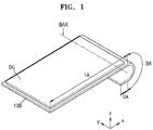
- FIG. 1 is a schematic perspective view of a part of a display apparatus according to an embodiment of the invention.
- a substrate 100 that is a part of the display apparatus is partially bent, and thus, the display apparatus also has a partially bent shape like the substrate 100.
- the substrate 100 of the display apparatus includes a bent area BA extending in a first direction (+y direction).
- the bent area BA is located between a first area 1A and a second area 2A in a second direction (+x direction) crossing the first direction.
- the substrate 100 is bent about a bending axis BAX that extends in the first direction (+y direction) as shown in FIG. 1 .
- tensile stress may be applied to an upper surface (an outer surface) of the substrate 100 and compressive stress may be applied to a lower surface (an inner surface) of the substrate 100.
- the substrate 100 may include various materials having flexible or bendable characteristics, e.g., polymer resins such as polyethersulphone (PES), polyacrylate (PAR), polyetherimide (PEI), polyethylene naphthalate (PEN), polyethyleneterephthalate (PET), polyphenylene sulfide (PPS), polyarylate, polyimide (PI), polycarbonate (PC), and cellulose acetate propionate (CAP).
- a display unit DU including a display device and a thin film transistor may be located at the first area 1A. If necessary, the display unit DU may be extended to the bent area BA or even to the second area 2A.
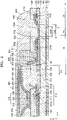
- FIGS. 2 to 4 are schematic cross-sectional views of processes of manufacturing the display apparatus of FIG. 1 .
- a display panel as shown in FIG. 2
- the first area 1A of the substrate 100 includes a display area DA.
- the first area 1A may further include a part of a non-display area at an outer portion of the display area DA, in addition to the display area DA, as shown in FIG. 2 .
- the second area 2A may also include the non-display area.
- a display unit including a display device, such as an organic light-emitting device 300, and also including a thin film transistor 210, may be located in the first area 1A.
- the substrate 100 includes the bent area BA between the first area 1A and the second area 2A so as to be bent at the bent area BA to have a shape as shown in FIG. 1 .
- the display panel includes a protective film 170 at a lower surface of the substrate 100, that is, in a direction (-z direction) that is opposite to a direction of the display unit (+z direction).
- the protective film 170 may be attached to the lower surface of the substrate 100 via an adhesive layer 180.
- the thin film transistor 210 to which the organic light-emitting device 300 is electrically connected, may be in the display area DA of the display panel, similarly to the display device such as the organic light-emitting device 300. Electric connection of the organic light-emitting device 300 to the thin film transistor 210 may be understood that a pixel electrode 310 is electrically connected to the thin film transistor 210.
- a thin film transistor may also be at a peripheral area on the outer portion of the display area DA on the substrate 100.
- the thin film transistor on the peripheral area may be, for example, a part of a circuit unit for controlling electric signals applied to the display area DA.
- the thin film transistor 210 may include a semiconductor layer 211 including amorphous silicon, polycrystalline silicon, or an organic semiconductor material.
- the thin film transistor 210 may also include a gate electrode 213, a source electrode 215a, and a drain electrode 215b.
- a gate insulating layer 120 may be between the semiconductor layer 211 and the gate electrode 213, the gate insulating layer 120 including an inorganic material, such as silicon oxide, silicon nitride, and/or silicon oxynitride.
- an interlayer insulating layer 130 may be on the gate electrode 213, and the source electrode 215a and the drain electrode 215b may be on the interlayer insulating layer 130, the interlayer insulating layer 130 including an inorganic material such as silicon oxide, silicon nitride, and/or silicon oxynitride.
- the insulating layers including the inorganic material may be formed through chemical vapor deposition (CVD) or atomic layer deposition (ALD). This will be applied to other embodiments and modifications thereof that will be described later.
- a buffer layer 110 may be between the thin film transistor 210 and the substrate 100.
- the buffer layer 110 may include an inorganic material, such as silicon oxide, silicon nitride, and/or silicon oxynitride.
- the buffer layer 110 may improve smoothness of the upper surface of the substrate 100, or may prevent or reduce infiltration of impurities from the substrate 100 into the semiconductor layer 211 of the thin film transistor 210.
- a planarization layer 140 may be arranged on the thin film transistor 210.
- the planarization layer 140 may planarize an upper portion of a protective layer that covers the thin film transistor 210, and the organic light-emitting device 300 may be arranged on the planarization layer 140.
- the planarization layer 140 may include, for example, an organic material such as acryl, benzocyclobutene (BCB), polyimide, and hexamethyldisiloxane (HMDSO).
- the planarization layer 140 has a single-layered structure, but the planarization layer 140 may be variously modified.
- the planarization layer 140 may have a multi-layered structure.
- the planarization layer 140 may have an opening at an outer portion of the display area DA, so that a part of the planarization layer 140 in the display area DA and another part of the planarization layer 140 in the second area 2A may be physically separate from each other. Then, external impurities may be unable to reach the display area DA via the planarization layer 140.
- the organic light-emitting device 300 may be on the planarization layer 140, the organic light-emitting device 300 including the pixel electrode 310, an opposite electrode 330, and an intermediate layer 320 that is between the pixel electrode 310 and the opposite electrode 330 and that includes an emission layer.
- the pixel electrode 310 may contact one of the source electrode 215a and the drain electrode 215b via an opening formed in the planarization layer 140, and may be electrically connected to the thin film transistor 210, as shown in FIG. 2 .
- a pixel defining layer 150 may be on the planarization layer 140.
- the pixel defining layer 150 includes openings respectively corresponding to sub-pixels, that is, includes at least an opening exposing a center portion of the pixel electrode 310, to define pixels. Also, in the example shown in FIG. 2 , the pixel defining layer 150 increases a distance between an edge of the pixel electrode 310 and the opposite electrode 330, which is above the pixel electrode 310, to prevent an arc, or electric short, from generating at the edge of the pixel electrode 310.
- the pixel defining layer 150 may include an organic material, for example, polyimide or HMDSO.
- the intermediate layer 320 of the organic light-emitting device 300 may include low-molecular weight organic materials or polymer organic materials.
- the intermediate layer 320 may include a hole injection layer (HIL), a hole transport layer (HTL), an emission layer (EML), an electron transport layer (ETL), and/or an electron injection layer (EIL) in a single or multiple-layered structure.
- HIL hole injection layer
- HTL hole transport layer
- EML emission layer
- ETL electron transport layer
- EIL electron injection layer
- the low-molecular weight organic materials may be deposited by a vacuum deposition method.
- the intermediate layer 320 may include a hole transport layer (HTL) and an emission layer (EML).
- HTL may include PEDOT
- EML may include a poly-phenylenevinylene (PPV)-based or polyfluorene-based polymer material.
- the intermediate layer 320 above may be formed by a screen printing method, an inkjet printing method, or a laser induced thermal imaging (LITI) method.
- LITI laser induced thermal imaging
- the intermediate layer 320 is not limited to the above example, and may have various structures.
- the intermediate layer 320 may include a layer that is integrally formed over a plurality of pixel electrodes 310, or may include a layer that is patterned to correspond to each of the plurality of pixel electrodes 310.
- the opposite electrode 330 is arranged above the display area DA, and as shown in FIG. 2 , may cover the display area DA. That is, the opposite electrode 330 may be integrally formed with respect to a plurality of organic light-emitting devices, so as to correspond to, or cover, a plurality of pixel electrodes 310.
- an encapsulation layer 400 may cover the organic light-emitting device 300 to protect the organic light-emitting device 300.
- the encapsulation layer 400 covers the display area DA, and may also extend outside the display area DA.
- the encapsulation layer 400 may include a first inorganic encapsulation layer 410, an organic encapsulation layer 420, and a second inorganic encapsulation layer 430, as shown in FIG. 2 .
- the first inorganic encapsulation layer 410 covers the opposite electrode 330, and may include silicon oxide, silicon nitride, and/or silicon oxynitride. If suitable, other layers, such as a capping layer, may be arranged between the first inorganic encapsulation layer 410 and the opposite electrode 330. Because the first inorganic encapsulation layer 410 is formed to have a shape corresponding to a structure thereunder, the first inorganic encapsulation layer 410 may have an uneven upper surface.
- the organic encapsulation layer 420 covers the first inorganic encapsulation layer 410, and unlike the first inorganic encapsulation layer 410, the organic encapsulation layer 420 may have an even, or planar, upper surface. In more detail, the organic encapsulation layer 420 may have a roughly, or substantially, even upper surface at a portion corresponding to the display area DA.
- the organic encapsulation layer 420 may include at least one material selected from the group consisting of polyethylene terephthalate, polyethylene naphthalate, polycarbonate, polyimide, polyethylene sulfonate, polyoxymethylene, polyarylate, and hexamethyldisiloxane.
- the second inorganic encapsulation layer 430 covers the organic encapsulation layer 420, and may include silicon oxide, silicon nitride, and/or silicon oxynitride.
- the second inorganic encapsulation layer 430 may contact the first inorganic encapsulation layer 410 at an edge thereof at an outer portion of the display area DA, thereby preventing exposure of the organic encapsulation layer 420 to the outside.
- the encapsulation layer 400 includes the first inorganic encapsulation layer 410, the organic encapsulation layer 420, and the second inorganic encapsulation layer 430, even if there is a crack in the encapsulation layer 400 in the above multi-layered structure, the crack may be disconnected, or may be stopped, between the first inorganic encapsulation layer 410 and the organic encapsulation layer 420, or between the organic encapsulation layer 420 and the second inorganic encapsulation layer 430. As such, forming of a path through which external moisture or oxygen may infiltrate into the display area DA may be prevented or reduced.
- processes of forming a touch electrode of various patterns for implementing a touch screen function, or of forming a touch protective layer for protecting the touch electrode on the encapsulation layer 400 may be further performed.
- the display panel includes the protective film 170 on the lower surface of the substrate 100, that is, the surface that is in an opposite direction (-z direction) to the direction of the surface on which the display unit is located (+z direction).
- the protective film 170 may include polyethylene terephthalate (PET).
- PET polyethylene terephthalate
- the protective film 170 may be adhered to the lower surface of the substrate 100 via the adhesive layer 180.
- the adhesive layer 180 may include, for example, a pressure sensitive adhesive (PSA). A point in time at which the protective film 170 is attached to the lower surface of the substrate 100 may vary depending on circumstances.
- PSA pressure sensitive adhesive
- a carrier substrate which is solid, may be located under the mother substrate to easily handle the mother substrate, which has flexible or bendable characteristics, during the manufacturing processes.
- the carrier substrate may be separated from the mother substrate.
- the carrier substrate may be separated from the mother substrate after forming a touch electrode and/or a touch protective layer for protecting the touch electrode on the encapsulation layers 400.
- the protective film 170 is attached to a surface of the mother substrate that contacted the carrier substrate. In this state, the mother substrate and the protective film 170 are cut to obtain a plurality of display panels.
- the substrate 100 may be understood as a substrate cut from the mother substrate.
- a polarization plate 520 is attached to the encapsulation layer 400 by an optically clear adhesive (OCA) 510, and if suitable, a printed circuit board or an electronic chip may be attached to the second area 2A. If there is a touch electrode or a touch protective layer on the encapsulation layer 400, the OCA 510 and the polarization plate 520 may be located over the above elements. In addition, a bending protection layer (BPL) 600 may be at an outer portion of the display area or at a portion outside the display area DA.
- OCA optically clear adhesive
- BPL bending protection layer
- a single display unit may be formed on one substrate 100.
- a carrier substrate that is solid may be located under the substrate 100 to easily handle the substrate 100 having flexible or bendable characteristics during the manufacturing processes.
- the carrier substrate may be separated from the substrate 100.
- the protective film 170 may be attached to the surface of the substrate 100 toward the carrier substrate.
- the polarization plate 520 may be attached to the encapsulation layer 400 or to the touch protective layer via the OCA 510, and if suitable, a printed circuit board or an electronic chip may be attached to the second area 2A.
- the BPL 600 may be formed on an outer portion of the display area DA.
- the polarization plate 520 may reduce reflection of external light. For example, when external light that passed through the polarization plate 520 is reflected by an upper surface of the opposite electrode 330, and that then passes through the polarization plate 520 again, the external light passes through the polarization plate 520 twice, and a phase of the external light may be changed. Therefore, a phase of reflected light is different from the phase of the external light entering the polarization plate 520 so that a destructive interference occurs. Accordingly, reflection of the external light may be reduced, and visibility of displayed images may be improved.
- the OCA 510 and the polarization plate 520 may cover the opening in the planarization layer 140, as shown in FIG. 2 .
- the method of manufacturing the display apparatus according to the embodiment need not include forming the polarization plate 520, and if suitable, the polarization plate 520 may be omitted or replaced with another component. For example, instead of attaching the polarization plate 520, a black matrix and a color filter may be formed to reduce the reflection of external light.
- the BPL 600 may be over a first conductive layer 215c, corresponding at least to the bent area BA.
- a stack structure When a stack structure is bent, there is a stress neutral plane in the stack structure. If there is no BPL 600, when the substrate 100 is bent, an excessive tensile stress may be applied to the first conductive layer 215c in the bent area BA, because the location of the first conductive layer 215c may not correspond to a stress neutral plane.
- a location of the stress neutral plane in the structure including the substrate 100, the first conductive layer 215c, and the BPL 600 may be adjusted. Therefore, the stress neutral plane may be adjusted to be around the first conductive layer 215c via the BPL 600, and thus, the tensile stress applied to the first conductive layer 215c may be reduced.
- the BPL 600 may extend to an end of the substrate 100 in the display apparatus, unlike the example of FIG. 2 .
- the first conductive layer 215c, a second conductive layer 213b, and/or other conductive layers electrically connected to the first and second conductive layers 215c and 213b might not be covered at least partially by the interlayer insulating layer 130 or the planarization layer 140, but may instead be electrically connected to various electronic devices or printed circuit boards.
- the first conductive layer 215c, the second conductive layer 213b, and/or the other conductive layers electrically connected to the first and second conductive layers 215c and 213b may have portions that are electrically connected to the various electronic devices or to the printed circuit boards.
- the electrically connected portions may be protected against external impurities such as moisture, and thus, the BPL 600 may cover the electrically connected portions to perform as a protective layer as well.
- the BPL 600 may extend to, for example, the end of the substrate 100 of the display apparatus.
- an upper surface of the BPL 600 in a direction toward the display area DA (-x direction) coincides with an upper surface of the polarization plate 520 (in +z direction), but one or more embodiments are not limited thereto.
- an end of the BPL 600 in a direction toward the display area DA (-x direction) may partially cover an upper surface of the polarization plate 520 at the edge of the polarization plate 520. Otherwise, the end of the BPL 600 in the direction toward the display area DA (-x direction) might not contact the polarization plate 520 and/or the OCA 510.
- a laser beam is irradiated to at least a portion of the protective film 170 corresponding to the bent area BA so that the protective film 170 may have an opening 170OP corresponding to the bent area BA, as shown in FIG. 4 .
- the laser beam is irradiated to the portion of the protective film 170, wherein the portion of the protective film 170 corresponds to an uneven surface 160a of an organic material layer 160, which will be described later.
- inner side surfaces 170a and 170b defining the opening 170OP are inclined with respect to the lower surface of the substrate 100.
- the opening 170OP may extend in the first direction (+y direction) such that a part of the protective film 170 corresponding to the first area 1A is separated from a part of the protective film 170 corresponding to the second area 2A.
- the substrate 100 may be bent at the bent area BA so that the display panel may have the shape shown in FIG. 1 .
- FIG. 5 is a schematic cross-sectional view of a part of the display apparatus of FIG. 1 , and shows the substrate 100, the protective film 170, and the adhesive layer 180.
- the substrate 100 may be bent at the bent area BA.
- the protective film 170 protects the lower surface of the substrate 100, and accordingly, may have a stiffness or rigidity of its own. Accordingly, when the substrate 100 is bent in a state where the protective film 170 has low flexibility, the protective film 170 may be otherwise separated from the substrate 100.
- the protective film 170 includes the opening 170OP corresponding to the bent area BA. Accordingly, the separation between the protective film 170 and the substrate 100 may be effectively prevented.
- the inner side surfaces 170a and 170b of the opening 170OP in the protective film 170 are inclined with respect to the lower surface of the substrate 100. Accordingly, the thickness of the protective film 170 may decrease toward the opening 170OP. Accordingly, even when stress is generated at the portion adjacent to the opening 170OP of the protective film 170 as the substrate 100 is bent at the bent area BA, the amount of stress generated from the portion may be reduced due to the decreasing thickness of the protective film 170 toward the opening 170OP. Accordingly, the separation of the protective film 170 from the substrate 100 may be effectively prevented.
- the bent area BA may be located within the opening 170OP of the protective film 170, and it may be understood that an area of the opening 170OP in the protective film 170 is greater than that of the bent area BA, as shown in FIG. 5 .
- FIG. 6 which is a schematic cross-sectional view of a part of a display apparatus according to an embodiment
- the opening 170OP of the protective film 170 may be located within the bent area BA, meaning that the area of the bent area BA may be greater than that of the opening 170OP in the protective film 170. Even in the embodiment shown in FIG.
- the thickness of the protective film 170 around the opening 170OP decreases toward the opening 170OP, as described above with respect to the embodiment shown in FIG. 5 , and the stress generated from the opening 170OP may be reduced. Accordingly, separation of the protective film 170 from the substrate 100 may be effectively prevented.
- the buffer layer 110, the gate insulating layer 120, and the interlayer insulating layer 130 including the inorganic material shown in FIGS. 2 to 4 may be referred to as a first inorganic insulating layer.
- the first inorganic insulating layer may include a first opening corresponding to the bent area BA, as shown in FIGS. 2 to 4 . That is, the buffer layer 110, the gate insulating layer 120, and the interlayer insulating layer 130 may respectively include openings 110a, 120a, and 130a corresponding to the bent area BA. That the first opening corresponds to the bent area BA may denote that the first opening overlaps with the bent area BA. Here, an area of the first opening may be greater than that of the bent area BA. To do this, in FIGS.
- a width OW of the first opening is greater than that of the bent area BA.
- the area of the first opening may be defined as an area of one of the openings 110a, 120a, and 130a respectively of the buffer layer 110, the gate insulating layer 120, and the interlayer insulating layer 130 that has a smallest area or width.
- the area of the first opening is described to be defined by an area of the opening 110a in the buffer layer 110.
- an inner side surface of the opening 110a of the buffer layer 110 and an inner side surface of the opening 120a in the gate insulating layer 120 are described to correspond to each other, but one or more embodiments are not limited thereto.
- an area of the opening 120a of the gate insulating layer 120 may be greater than that of the opening 110a in the buffer layer 110.
- the area of the first opening may be also defined as an area of the one among a smallest of the openings 110a, 120a, and 130a of the buffer layer 110, the gate insulating layer 120, and the interlayer insulating layer 130, respectively.
- the display unit when the display unit is formed, an organic material layer 160 that fills at least a part of the first opening of the first inorganic insulating layer is formed. In FIGS. 2 to 4 , the organic material layer 160 completely fills the first opening.
- the display unit includes the first conductive layer 215c that extends from the first area 1A toward the second area 2A through the bent area BA, and that is over the organic material layer 160.
- the first conductive layer 215c may be on one of the inorganic insulating layers, such as the interlayer insulating layer 130, if the organic material layer 160 does not exist.
- the first conductive layer 215c may be formed during a same process as (e.g., simultaneously with) a source electrode 215a or a drain electrode 215b by using the same material as that of the source electrode 215a or the drain electrode 215b.
- the display panel is bent at the bent area BA, as shown in FIG. 5 .
- the substrate 100 is bent at the bent area BA, although tensile stress may be applied to the first conductive layer 215c, occurrence of defects in the first conductive layer 215c during the bending process may be prevented or reduced in the display apparatus according to the embodiment.
- the first inorganic insulating layer including the buffer layer 110, the gate insulating layer 120, and/or the interlayer insulating layer 130 does not include the opening corresponding to the bent area BA, but instead continuously extends from the first area 1A to the second area 2A, and if the first conductive layer 215c is thereon, relatively large tensile stress is applied to the first conductive layer 215c during bending of the substrate 100.
- the first inorganic insulating layer has greater rigidity/stiffness than that of the organic material layer 160, cracks are more likely to form in the first inorganic insulating layer in the bent area BA, and when a crack occurs in the first inorganic insulating layer, the crack may also occur in the first conductive layer 215c on the first inorganic insulating layer, and thus the probability of generating defects, such as disconnection in the first conductive layer 215c increases greatly.
- the first inorganic insulating layer includes the first opening corresponding to the bent area BA, and the part of the first conductive layer 215c, which corresponds to the bent area BA, is on the organic material layer 160 that at least partially fills the first opening of the first inorganic insulating layer. Because the first inorganic insulating layer includes the first opening corresponding to the bent area BA, the possibility of cracks occurring in the first inorganic insulating layer is reduced, and the organic material layer 160 is less likely to have cracks due to characteristics of the organic material.
- the occurrence of cracks in the portion of the first conductive layer 215c on the organic material layer 160 may be prevented or reduced, wherein the portion of the first conductive layer 215c corresponds to the bent area BA. Because the organic material layer 160 has a lower hardness than that of an inorganic material layer, the organic material layer 160 may absorb the tensile stress generated due to the bending of the substrate 100 to reduce concentration of the tensile stress on the first conductive layer 215c.
- second conductive layers 213a and 213b may be formed, in addition to the first conductive layer 215c.
- the second conductive layers 213a and 213b may be formed in the first area 1A and/or the second area 2A (or respectively formed in the first and second areas 1A and 2A) at a different layer level than the first conductive layer 215c, and may be electrically connected to the first conductive layer 215c.
- the second conductive layers 213a and 213b may include the same material as that of the gate electrode 213 of the thin film transistor 210, and are at the same layer as the gate electrode 213 (i.e., on the gate insulating layer 120).
- first conductive layer 215c contacts the second conductive layers 213a and 213b via respective contact holes formed in the interlayer insulating layer 130.
- second conductive layer 213a is located in the first area 1A
- second conductive layer 213b is located in the second area 2A.
- the second conductive layer 213a in the first area 1A may be electrically connected to the thin film transistor 210 within the display area DA, and accordingly, the first conductive layer 215c may be electrically connected to the thin film transistor 210 of the display area DA via the second conductive layer 213a.
- the second conductive layer 213b in the second area 2A may also be electrically connected to the thin film transistor 210 of the display area DA via the first conductive layer 215c.
- the second conductive layers 213a and 213b that are at an outer portion of the display area DA may be electrically connected to the elements in the display area DA, or may extend toward the display area DA so that at least some parts of the second conductive layers 213a and 213b may be located in the display area DA.
- the display panel is bent at the bent area BA, as shown in FIG. 5 .
- the tensile stress may be applied to the elements in the bent area BA.
- the first conductive layer 215c crossing over the bent area BA includes a material having high flexibility, so that defects such as cracks in the first conductive layer 215c or disconnection of the first conductive layer 215c may be prevented.
- the second conductive layers 213a and 213b including a material having an elongation rate that is lower than that of the first conductive layer 215c, and including electrical/physical characteristics that are different from those of the first conductive layer 215c, are formed in the first area 1A and/or the second area 2A, and thus, an efficiency of transferring electric signals may be improved, or a defect rate during the manufacturing processes of the display apparatus may be reduced.
- the second conductive layers 213a and 213b may include molybdenum, and the first conductive layer 215c may include aluminum.
- the first conductive layer 215c and the second conductive layers 213a and 213b may have multi-layered structures, if suitable.
- At least a part of an upper portion of the second conductive layer 213b in the second area 2A may instead be uncovered by the planarization layer 140, and may instead be exposed to the outside to be electrically connected to various electronic devices or printed circuit boards.
- the organic material layer 160 may have the uneven surface 160a at least partially in an upper surface thereof (in +z direction). Because the organic material layer 160 includes the uneven surface 160a, the first conductive layer 215c on the organic material layer 160 may include an upper surface and/or a lower surface having a shape corresponding to the uneven surface 160a of the organic material layer 160.
- the tensile stress is applied to the first conductive layer 215c.
- an amount of the tensile stress applied to the first conductive layer 215c may be reduced. That is, the tensile stress that may occur during the bending process may be reduced through deformation of the organic material layer 160 having a low rigidity/stiffness.
- the shape of the first conductive layer 215c having the uneven shape at least before the bending process is deformed to correspond to the shape of the organic material layer 160 changed due to the bending, and thus, generation of a defect, such as disconnection in the first conductive layer 215c, may be effectively prevented.
- the uneven surface 160a is formed at least partially at the upper surface of the organic material layer 160 (in +z direction), and thus, a surface area of the upper surface of the organic material layer 160, and respective surface areas of the upper and lower surfaces of the first conductive layer 215c within the first opening, may be increased.
- a relatively large surface area of the upper surface of the organic material layer 160 and the upper and lower surfaces of the first conductive layer 215c may enable a large deformation margin for reducing the tensile stress caused by the bending of the substrate 100.
- the lower surface of the first conductive layer 215c has a shape corresponding to the uneven surface 160a of the organic material layer 160.
- the upper surface of the first conductive layer 215c may have an uneven surface that does not correspond to the shape of the uneven surface 160a of the organic material layer 160.
- the uneven surface 160a of the organic material layer 160 may be formed in various ways.
- a photoresist material may be used to form the organic material layer 160, and an exposure amount may vary depending on locations of the upper surface of the organic material layer 160, which is in a flat state during the manufacturing processes, by using a slit mask or a half-tone mask so that a certain part may be etched (removed) relatively more than other parts.
- the more etched part may be understood as a concave portion in the upper surface of the organic material layer 160.
- the forming of the organic material layer 160 in the display apparatus according to one or more embodiments is not limited to the above example. For example, after forming the organic material layer 160 having the upper surface that is flat, a certain portion may be removed by using a dry etching method.
- the organic material layer 160 may include a plurality of grooves extending in the first direction (+y direction) in the upper surface (in the +z direction) thereof.
- the shape of the upper surface of the first conductive layer 215c on the organic material layer 160 corresponds to the shape of the upper surface of the organic material layer 160.
- the organic material layer 160 may have the uneven surface 160a only within the first opening of the first inorganic insulating layer. In FIGS. 2 to 4 , a width UEW of the uneven surface 160a of the organic material layer 160 is less than a width OW of the first opening of the first inorganic insulating layer. If the organic material layer 160 has the uneven surface 160a both inside and outside the first opening in the first inorganic insulating layer, the organic material layer 160 has the uneven surface 160a near the internal surface of the opening 110a in the buffer layer 110, the internal surface of the opening 120a in the gate insulating layer 120, or the internal surface of the opening 130a in the interlayer insulating layer 130.
- the organic material layer 160 has a relatively smaller thickness on depressed portions than on protruding portions, and thus, when the depressed portions are located around the internal surface of the opening 110a in the buffer layer 110, the internal surface of the opening 120a in the gate insulating layer 120, or the internal surface of the opening 130a in the interlayer insulating layer 130, the organic material layer 160 may be disconnected. Therefore, the organic material layer 160 may have the uneven surface 160a only within the first opening of the first inorganic insulating layer, and accordingly, the disconnection of the organic material layer 160 around the internal surface of the opening 110a in the buffer layer 110, the internal surface of the opening 120a of the gate insulating layer 120, or the internal surface of the opening 130a in the interlayer insulating layer 130 may be prevented.
- the organic material layer 160 may have the uneven surface 160a in the bent area BA. Therefore, an area of the uneven surface 160a of the organic material layer 160 may be greater than an area of the bent area BA, and may be smaller than the area of the first opening. That is, as shown in FIGS. 2 to 4 , the width UEW of the uneven surface 160a of the organic material layer 160 is greater than the width of the bent area BA and smaller than the width OW of the first opening.
- the organic material layer 160 may be formed during a same process as (e.g., simultaneously with) the layer including the organic insulating material, and moreover, the layer including the organic insulating material and the organic material layer 160 may be integrally formed with each other.
- the organic insulating material may include polyethylene terephthalate, polyethylene naphthalate, polycarbonate, polyimide, polyethylene sulfonate, polyoxymethylene, polyarylate, and/or hexamethyldisiloxane.
- FIG. 7 is a schematic cross-sectional view of a part of a display apparatus according to an embodiment.
- the display apparatus of FIG. 7 is not bent.
- the display apparatus is not in a bent state (e.g., not yet in a bent state) for convenience of description.
- a width of the opening 170OP of the protective film 170 is equal to the width UEW of the uneven surface 160a in the organic material layer 160, but the embodiment is not limited thereto.
- the width of the opening 170OP of the protective film 170 may be less than the width UEW of the uneven surface 160a of the organic material layer 160.
- the adhesive layer 180 may remain in an area corresponding to the opening 170OP, as shown in FIGS. 4 to 7 .
- the display apparatus includes the adhesive layer 180 interposed between the substrate 100 and the protective film 170, and the adhesive layer 180 may be integrally formed throughout the first area 1A, the bent area BA, and the second area 2A.
- the substrate 100 When the opening 170OP is formed by irradiating the laser beam to the protective film 170, the substrate 100 is not supposed to be damaged. Therefore, damage to the substrate 100 may be avoided by forming the opening 170OP in the protective film 170, and by ensuring that the adhesive layer 180 remains in the opening 170OP, rather than by removing the adhesive layer 180 between the protective film 170 and the substrate 100. That is, the adhesive layer 180 may protect a portion of the substrate 100, which corresponds to the opening 170OP, during the manufacturing processes. In addition, if the adhesive layer 180 includes a PSA, the stress generated in the adhesive layer 180 within the bent area BA may be reduced due to characteristics of the PSA even when the substrate 100 is bent at the bent area BA.
- the adhesive layer 180 may have a constant or consistent thickness throughout the first area 1A, the bent area BA, and the second area 2A.
- FIG. 8 which is a schematic cross-sectional view of a part of a display apparatus according to an embodiment, the adhesive layer 180 corresponding to the opening 170OP may be partially removed (e.g., thinned) when the opening 170OP is formed in the protective film 170. Accordingly, a thickness t1 of the adhesive layer 180 at a portion corresponding to the opening 170OP may be less than a thickness t2 of the adhesive layer 180 at portions/areas between the substrate 100 and the protective film 170.
- the adhesive layer 180 also remains in the opening 170OP of the protective film 170, and thus, damage to the substrate 100 may be prevented during forming the opening 170OP, and the adhesive layer 180 may protect the substrate 100 corresponding to the opening 170OP during the manufacturing processes.
- the adhesive layer 180 may have an uneven surface 180EP (in the -z direction) corresponding to the opening 170OP.
- the uneven surface 180EP is irregular, that is, a width, a height, and an interval of peaks and/or valleys of the uneven surface 180EP are not constant.
- the adhesive layer 180 includes the uneven surface 180EP in the portion corresponding to the opening 170OP, the stress generated in the adhesive layer 180 when the substrate 100 is bent be dispersed instead of being concentrated at one point.
- the protective film 170 has the thickness around the opening 170OP, wherein the thickness is gradually smaller toward the opening 170OP at a constant rate.
- FIG. 10 which is a schematic cross-sectional view of a part of a display apparatus according to an embodiment
- a thickness of the protective film 170 might not decrease at a constant rate.
- a rate of reduction of the thickness may decrease toward the opening 170OP. In this case, as shown in FIG.
- inner side surfaces 170a and 170b at the opening 170OP in the protective film 170, along with the surface of the adhesive layer 180 within the opening 170OP, may form an entirely concave shape. Even in the structure shown in FIG. 10 , the surface of the adhesive layer 180 corresponding to the opening 170OP might not be flat, but may instead have an uneven surface. Alternatively, the adhesive layer 180 may have a constant thickness throughout the first area 1A, the bent area BA, and the second area 2A.
- the protective film 170 has a first portion(s) 171 having a constant thickness, a second portion(s) 172 that is adjacent the opening 170OP and has a thickness that decreases toward the opening 170OP, and a third portion(s) 173 located between the first portion 171 and the second portion 172 that is thicker than the first portion 171.
- the adhesive layer 180 may also have an uneven surface (e.g., 180EP) in the part corresponding to the opening 170OP as shown in FIG. 9 .
- a laser beam may be additionally irradiated to the third portion 173 to remove the particles, so that the third portion 173 is not present between the first portion 171 and the second portion 172. That is, the protective film 170 may have a constant thickness except at the second portion 172. In this case, because a bonding strength between particles, and a bonding strength between the particles and the surface of the protective film 170, are lower than a bonding strength between the elements in the protective film 170, only the particles may be removed without damaging the surface of the protective film 170.
- the protective film 170 may include a plurality of openings 171OP, 172OP, and 173OP respectively corresponding to the bent area BA.
- Each of the plurality of openings 171OP, 172OP, and 173OP may extend in the first direction (+y direction), and may be implemented by irradiating the laser beam only to their corresponding parts.
- the protective film 170 includes the plurality of openings 171OP, 172OP, and 173OP corresponding to the bent area BA, separation between the protective film 170 and the substrate 100 when the substrate 100 is bent may be prevented effectively.
- an inner side surface 170a of the opening 171OP that is the last opening in the direction toward the display area DA (the inner side surface 170a being in a direction toward the display area DA (-x direction) that is opposite to the second direction (+x direction)), may be inclined with respect to the lower surface of the substrate 100.
- the thickness t1 of the adhesive layer 180 corresponding to the plurality of openings 171OP, 172OP, and 173OP is less than the thickness t2 of the adhesive layer 180 between the substrate 100 and the protective film 170.
- the thickness of the adhesive layer 180 may be constant throughout the first area 1A, the bent area BA, and the second area 2A.
- the protective film 170 has been described to have the opening 170OP above, but one or more embodiments are not limited thereto.
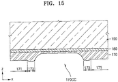
- the protective film 170 may include a concave portion 170CC corresponding to the bent area BA.
- the concave portion 170CC may be implemented by not completely removing the portion of the protective film 170 corresponding to the bent area BA.
- the concave portion 170CC may have a first part 170d where a thickness of the concave portion is gradually reduced toward a center of the concave portion 170CC.
- the thickness of the concave portion 170CC in the first part 170d may be gradually reduced toward the bending axis.
- the concave portion 170CC may have a second part 170c where the thickness of the concave portion is constant. In the latter case, the second part 170c may be located around the center of the concave portion 170CC.
- the protective film 170 protects the lower surface of the substrate 100
- the protective film 170 may have stiffness of its own (e.g., may be relatively rigid). Accordingly, if the protective film 170 has low flexibility, the protective film 170 may be separated from the substrate 100 when the substrate 100 is bent. However, according to the display apparatus of the embodiment, because the protective film 170 includes the concave portion 170CC corresponding to the bent area BA, the separation between the protective film 170 and the substrate 100 may be effectively prevented.
- the bent area BA may correspond to the concave portion 170CC as shown in FIG. 13 .
- the bent area BA may be at the second part 170c (e.g., width of the bent area BA is less than width of the second part 170c).
- the second part 170c may be located in the bent area BA, if suitable (e.g., width of the second part 170c is less than width of the bent area BA).
- a rate of reduction of the thickness toward the center of the concave portion 170CC may not be constant.
- the reduction rate of the thickness may decrease toward the center of the concave portion 170CC.
- the protective film 170 includes a first portion(s) 171 having a constant thickness, and a third portion(s) 173 located between the first portion 171 and the concave portion 170CC, and having a thickness that is greater than a thickness of the first portion 171.
- the third portion 173 that is relatively thick is located around the concave portion 170CC of the protective film 170, degradation in performances of the protective film 170 around the concave portion 170CC may be prevented.
- the laser beam may be additionally irradiated to the third portion 173 to remove the attached particles, and the third portion 173 may be omitted. That is, the protective film 170 may have the constant thickness at portions other than the concave portion 170CC. In this case, because a bonding strength between the attached particles, and a bonding strength between the attached particles and the protective film 170, are lower than a coupling strength between the elements in the protective film 170, the attached particles may be removed without damaging the surface of the protective film 170.
- Embodiments of the invention are described above, but the embodiments are not limited thereto.
- a method of manufacturing the above display apparatus may be also included in the scope of the one or more embodiments of the invention.
- the display apparatus capable of reducing manufacturing costs and a defect rate during the manufacturing processes may be implemented.
Landscapes
- Engineering & Computer Science (AREA)
- Microelectronics & Electronic Packaging (AREA)
- Physics & Mathematics (AREA)
- Optics & Photonics (AREA)
- General Physics & Mathematics (AREA)
- Theoretical Computer Science (AREA)
- Electroluminescent Light Sources (AREA)
- Devices For Indicating Variable Information By Combining Individual Elements (AREA)
- Nonlinear Science (AREA)
- Mathematical Physics (AREA)
- Chemical & Material Sciences (AREA)
- Crystallography & Structural Chemistry (AREA)
- Preparation Of Compounds By Using Micro-Organisms (AREA)
- Measuring Pulse, Heart Rate, Blood Pressure Or Blood Flow (AREA)
- Compounds Of Unknown Constitution (AREA)
Abstract
Description
- One or more embodiments of the invention relate to a display apparatus capable of reducing manufacturing costs and a defective rate during manufacturing processes.
- In general, a display apparatus includes a display unit on a substrate. In such a display apparatus, at least a part of the display apparatus may be bent to improve visibility from various angles, and to reduce an area of a non-display area.
- However, in the related art, defects may occur during manufacture of a display apparatus that is bent, or manufacturing costs may excessively increase to produce the display apparatus that is bent.
- One or more embodiments of the invention include a display apparatus capable of reducing a defect rate during manufacturing processes, and capable of reducing manufacturing costs.
- Additional aspects will be set forth in part in the description that follows and, in part, will be apparent from the description, or may be learned by practice of the presented embodiments.
- According to one or more embodiments of the invention, a display apparatus includes a substrate including a bent area between a first area and a second area, and bent about a bending axis, a display unit over an upper surface of the substrate at the first area, and a protective film over a lower surface of the substrate that is opposite to the upper surface, and including an opening corresponding to the bent area, wherein an inner side surface of the opening is inclined with respect to the lower surface of the substrate.
- The display apparatus may further include an adhesive layer integrally formed throughout the first area, the bent area, and the second area between the substrate and the protective film.
- A portion of the adhesive layer corresponding to the opening may have a thickness that is less than a thickness of a portion of the adhesive layer between the substrate and the protective film.
- A portion of the protective film that is adjacent the opening may have a gradually decreasing thickness in a direction toward the opening.
- The gradually decreasing thickness may decrease at an inconsistent rate.
- The gradually decreasing thickness may decrease at a decreasing rate in the direction toward the opening.
- The protective film may include a first portion having a constant thickness, a second portion adjacent the opening, and having a thickness that gradually decreases in a direction toward the opening, and a third portion between the first portion and the second portion, and having a thickness that is greater than the thickness of the first portion.
- The bent area may be in the opening.
- The opening may be in the bent area.
- According to one or more embodiments of the invention, a display apparatus includes a substrate including a bent area between a first area and a second area, and bent about a bending axis, a display unit over an upper surface of the substrate in the first area, and a protective film over a lower surface of the substrate that is opposite to the upper surface, and including a concave portion corresponding to the bent area.
- The concave portion of the protective film may have a first part where a thickness of the concave portion gradually decreases toward a center of the concave portion.
- The thickness of the concave portion in the first part may decrease toward the center of the concave portion at an inconsistent rate.
- The thickness of the concave portion in the first part may decrease toward the center of the concave portion at a decreasing rate.
- The concave portion of the protective film may have a second part where the thickness of the concave portion is constant.
- The second part may correspond to the center of the concave portion.
- The protective film may include a first portion having a constant thickness, and a third portion between the first portion and the concave portion having a thickness that is greater than the thickness of the first portion.
- The bent area may be in the concave portion.
- According to the invention there is provided a display apparatus as set out in
claim 1 or 10. Optional features of the invention are set out inclaims 2 to 9 and 11 to 16. - These and/or other aspects will become apparent and more readily appreciated from the following description of the embodiments, taken in conjunction with the accompanying drawings in which:
-
FIG. 1 is a schematic perspective view of a part of a display apparatus according to an embodiment of the invention; -
FIGS. 2 to 4 are schematic cross-sectional views of processes of manufacturing the display apparatus ofFIG. 1 ; -
FIG. 5 is a schematic cross-sectional view of a part of the display apparatus ofFIG. 1 ; -
FIG. 6 is a schematic cross-sectional view of a part of a display apparatus according to an embodiment of the invention; -
FIG. 7 is a schematic cross-sectional view of a part of a display apparatus according to an embodiment of the invention; -
FIG. 8 is a schematic cross-sectional view of a part of a display apparatus according to an embodiment of the invention; -
FIG. 9 is a schematic cross-sectional view of a part of a display apparatus according to an embodiment of the invention; -
FIG. 10 is a schematic cross-sectional view of a part of a display apparatus according to an embodiment of the invention; -
FIG. 11 is a schematic cross-sectional view of a part of a display apparatus according to an embodiment of the invention; -
FIG. 12 is a schematic cross-sectional view of a part of a display apparatus according to an embodiment of the invention; -
FIG. 13 is a schematic cross-sectional view of a part of a display apparatus according to an embodiment of the invention; -
FIG. 14 is a schematic cross-sectional view of a part of a display apparatus according to an embodiment of the invention; and -
FIG. 15 is a schematic cross-sectional view of a part of a display apparatus according to an embodiment of the invention. - Features of the inventive concept and methods of accomplishing the same may be understood more readily by reference to the following detailed description of embodiments thereof and the accompanying drawings. Hereinafter, example embodiments will be described in more detail with reference to the accompanying drawings, in which like reference numbers refer to like elements throughout. The present invention, however, may be embodied in various different forms, and should not be construed as being limited to only the illustrated embodiments herein. Rather, these embodiments are provided as examples so that this disclosure will be thorough, and will convey the aspects and features of the present invention to those skilled in the art. Accordingly, processes, elements, and techniques that are not suitable to those having ordinary skill in the art for a complete understanding of the aspects and features of the present invention may not be described. Unless otherwise noted, like reference numerals denote like elements throughout the attached drawings and the written description, and thus, descriptions thereof will not be repeated. In the drawings, the relative sizes of elements, layers, and regions may be exaggerated for clarity.
- It will be understood that, although the terms "first," "second," "third," etc., may be used herein to describe various elements, components, regions, layers and/or sections, these elements, components, regions, layers and/or sections should not be limited by these terms. These terms are used to distinguish one element, component, region, layer or section from another element, component, region, layer or section. Thus, a first element, component, region, layer or section described below could be termed a second element, component, region, layer or section, without departing from the spirit and scope of the present invention.
- Spatially relative terms, such as "beneath," "below," "lower," "under," "above," "upper," and the like, may be used herein for ease of explanation to describe one element or feature's relationship to another element(s) or feature(s) as illustrated in the figures. It will be understood that the spatially relative terms are intended to encompass different orientations of the device in use or in operation, in addition to the orientation depicted in the figures. For example, if the device in the figures is turned over, elements described as "below" or "beneath" or "under" other elements or features would then be oriented "above" the other elements or features. Thus, the example terms "below" and "under" can encompass both an orientation of above and below. The device may be otherwise oriented (e.g., rotated 90 degrees or at other orientations) and the spatially relative descriptors used herein should be interpreted accordingly.
- It will be understood that when an element, layer, region, or component is referred to as being "on," "connected to," or "coupled to" another element, layer, region, or component, it can be directly on, connected to, or coupled to the other element, layer, region, or component, or one or more intervening elements, layers, regions, or components may be present. In addition, it will also be understood that when an element or layer is referred to as being "between" two elements or layers, it can be the only element or layer between the two elements or layers, or one or more intervening elements or layers may also be present.
- In the following examples, the x-axis, the y-axis and the z-axis are not limited to three axes of a rectangular coordinate system, and may be interpreted in a broader sense. For example, the x-axis, the y-axis, and the z-axis may be perpendicular to one another, or may represent different directions that are not perpendicular to one another.
- The terminology used herein is for the purpose of describing particular embodiments only and is not intended to be limiting of the present invention. As used herein, the singular forms "a" and "an" are intended to include the plural forms as well, unless the context clearly indicates otherwise. It will be further understood that the terms "comprises," "comprising," "includes," and "including," when used in this specification, specify the presence of the stated features, integers, steps, operations, elements, and/or components, but do not preclude the presence or addition of one or more other features, integers, steps, operations, elements, components, and/or groups thereof. As used herein, the term "and/or" includes any and all combinations of one or more of the associated listed items. Expressions such as "at least one of," when preceding a list of elements, modify the entire list of elements and do not modify the individual elements of the list.
- As used herein, the term "substantially," "about," and similar terms are used as terms of approximation and not as terms of degree, and are intended to account for the inherent deviations in measured or calculated values that would be recognized by those of ordinary skill in the art. Further, the use of "may" when describing embodiments of the present invention refers to "one or more embodiments of the present invention." As used herein, the terms "use," "using," and "used" may be considered synonymous with the terms "utilize," "utilizing," and "utilized," respectively. Also, the term "exemplary" is intended to refer to an example or illustration.
- When a certain embodiment may be implemented differently, a specific process order may be performed differently from the described order. For example, two consecutively described processes may be performed substantially at the same time or performed in an order opposite to the described order.
- The electronic or electric devices and/or any other relevant devices or components according to embodiments of the present invention described herein may be implemented utilizing any suitable hardware, firmware (e.g. an application-specific integrated circuit), software, or a combination of software, firmware, and hardware. For example, the various components of these devices may be formed on one integrated circuit (IC) chip or on separate IC chips. Further, the various components of these devices may be implemented on a flexible printed circuit film, a tape carrier package (TCP), a printed circuit board (PCB), or formed on one substrate. Further, the various components of these devices may be a process or thread, running on one or more processors, in one or more computing devices, executing computer program instructions and interacting with other system components for performing the various functionalities described herein. The computer program instructions are stored in a memory which may be implemented in a computing device using a standard memory device, such as, for example, a random access memory (RAM). The computer program instructions may also be stored in other non-transitory computer readable media such as, for example, a CD-ROM, flash drive, or the like. Also, a person of skill in the art should recognize that the functionality of various computing devices may be combined or integrated into a single computing device, or the functionality of a particular computing device may be distributed across one or more other computing devices without departing from the scope of the present invention.
- Unless otherwise defined, all terms (including technical and scientific terms) used herein have the same meaning as commonly understood by one of ordinary skill in the art to which the present invention belongs. It will be further understood that terms, such as those defined in commonly used dictionaries, should be interpreted as having a meaning that is consistent with their meaning in the context of the relevant art and/or the present specification, and should not be interpreted in an idealized or overly formal sense, unless expressly so defined herein.
-
FIG. 1 is a schematic perspective view of a part of a display apparatus according to an embodiment of the invention. In the display apparatus according to the embodiment, asubstrate 100 that is a part of the display apparatus is partially bent, and thus, the display apparatus also has a partially bent shape like thesubstrate 100. - As shown in
FIG. 1 , thesubstrate 100 of the display apparatus according to the embodiment includes a bent area BA extending in a first direction (+y direction). The bent area BA is located between afirst area 1A and asecond area 2A in a second direction (+x direction) crossing the first direction. In addition, thesubstrate 100 is bent about a bending axis BAX that extends in the first direction (+y direction) as shown inFIG. 1 . In the bent area BA, tensile stress may be applied to an upper surface (an outer surface) of thesubstrate 100 and compressive stress may be applied to a lower surface (an inner surface) of thesubstrate 100. Thesubstrate 100 may include various materials having flexible or bendable characteristics, e.g., polymer resins such as polyethersulphone (PES), polyacrylate (PAR), polyetherimide (PEI), polyethylene naphthalate (PEN), polyethyleneterephthalate (PET), polyphenylene sulfide (PPS), polyarylate, polyimide (PI), polycarbonate (PC), and cellulose acetate propionate (CAP). A display unit DU including a display device and a thin film transistor may be located at thefirst area 1A. If necessary, the display unit DU may be extended to the bent area BA or even to thesecond area 2A. -
FIGS. 2 to 4 are schematic cross-sectional views of processes of manufacturing the display apparatus ofFIG. 1 . First, a display panel, as shown inFIG. 2 , is prepared. As shown inFIG. 2 , thefirst area 1A of thesubstrate 100 includes a display area DA. Thefirst area 1A may further include a part of a non-display area at an outer portion of the display area DA, in addition to the display area DA, as shown inFIG. 2 . Thesecond area 2A may also include the non-display area. A display unit including a display device, such as an organic light-emittingdevice 300, and also including athin film transistor 210, may be located in thefirst area 1A. Thesubstrate 100 includes the bent area BA between thefirst area 1A and thesecond area 2A so as to be bent at the bent area BA to have a shape as shown inFIG. 1 . - The display panel includes a
protective film 170 at a lower surface of thesubstrate 100, that is, in a direction (-z direction) that is opposite to a direction of the display unit (+z direction). Theprotective film 170 may be attached to the lower surface of thesubstrate 100 via anadhesive layer 180. A detailed structure of the display panel, to which theprotective film 170 is attached, will be described in more detail below. - The
thin film transistor 210, to which the organic light-emittingdevice 300 is electrically connected, may be in the display area DA of the display panel, similarly to the display device such as the organic light-emittingdevice 300. Electric connection of the organic light-emittingdevice 300 to thethin film transistor 210 may be understood that apixel electrode 310 is electrically connected to thethin film transistor 210. - If suitable, a thin film transistor may also be at a peripheral area on the outer portion of the display area DA on the
substrate 100. The thin film transistor on the peripheral area may be, for example, a part of a circuit unit for controlling electric signals applied to the display area DA. - The
thin film transistor 210 may include asemiconductor layer 211 including amorphous silicon, polycrystalline silicon, or an organic semiconductor material. Thethin film transistor 210 may also include agate electrode 213, asource electrode 215a, and adrain electrode 215b. To ensure an insulating property between thesemiconductor layer 211 and thegate electrode 213, agate insulating layer 120 may be between thesemiconductor layer 211 and thegate electrode 213, thegate insulating layer 120 including an inorganic material, such as silicon oxide, silicon nitride, and/or silicon oxynitride. - In addition, an
interlayer insulating layer 130 may be on thegate electrode 213, and thesource electrode 215a and thedrain electrode 215b may be on theinterlayer insulating layer 130, theinterlayer insulating layer 130 including an inorganic material such as silicon oxide, silicon nitride, and/or silicon oxynitride. The insulating layers including the inorganic material (e.g., thegate insulating layer 120 and the interlayer insulating layer 130) may be formed through chemical vapor deposition (CVD) or atomic layer deposition (ALD). This will be applied to other embodiments and modifications thereof that will be described later. - A
buffer layer 110 may be between thethin film transistor 210 and thesubstrate 100. Thebuffer layer 110 may include an inorganic material, such as silicon oxide, silicon nitride, and/or silicon oxynitride. Thebuffer layer 110 may improve smoothness of the upper surface of thesubstrate 100, or may prevent or reduce infiltration of impurities from thesubstrate 100 into thesemiconductor layer 211 of thethin film transistor 210. - A
planarization layer 140 may be arranged on thethin film transistor 210. For example, as shown inFIG. 2 , when the organic light-emittingdevice 300 is arranged over thethin film transistor 210, theplanarization layer 140 may planarize an upper portion of a protective layer that covers thethin film transistor 210, and the organic light-emittingdevice 300 may be arranged on theplanarization layer 140. Theplanarization layer 140 may include, for example, an organic material such as acryl, benzocyclobutene (BCB), polyimide, and hexamethyldisiloxane (HMDSO). InFIG. 2 , theplanarization layer 140 has a single-layered structure, but theplanarization layer 140 may be variously modified. For example, theplanarization layer 140 may have a multi-layered structure. - In addition, as shown in
FIG. 2 , theplanarization layer 140 may have an opening at an outer portion of the display area DA, so that a part of theplanarization layer 140 in the display area DA and another part of theplanarization layer 140 in thesecond area 2A may be physically separate from each other. Then, external impurities may be unable to reach the display area DA via theplanarization layer 140. - In the display area DA, the organic light-emitting
device 300 may be on theplanarization layer 140, the organic light-emittingdevice 300 including thepixel electrode 310, anopposite electrode 330, and anintermediate layer 320 that is between thepixel electrode 310 and theopposite electrode 330 and that includes an emission layer. Thepixel electrode 310 may contact one of thesource electrode 215a and thedrain electrode 215b via an opening formed in theplanarization layer 140, and may be electrically connected to thethin film transistor 210, as shown inFIG. 2 . - A
pixel defining layer 150 may be on theplanarization layer 140. Thepixel defining layer 150 includes openings respectively corresponding to sub-pixels, that is, includes at least an opening exposing a center portion of thepixel electrode 310, to define pixels. Also, in the example shown inFIG. 2 , thepixel defining layer 150 increases a distance between an edge of thepixel electrode 310 and theopposite electrode 330, which is above thepixel electrode 310, to prevent an arc, or electric short, from generating at the edge of thepixel electrode 310. Thepixel defining layer 150 may include an organic material, for example, polyimide or HMDSO. - The
intermediate layer 320 of the organic light-emittingdevice 300 may include low-molecular weight organic materials or polymer organic materials. When theintermediate layer 320 includes a low-molecular weight organic material, the intermediate layer may include a hole injection layer (HIL), a hole transport layer (HTL), an emission layer (EML), an electron transport layer (ETL), and/or an electron injection layer (EIL) in a single or multiple-layered structure. The low-molecular weight organic materials may be deposited by a vacuum deposition method. - When the
intermediate layer 320 includes a polymer material, theintermediate layer 320 may include a hole transport layer (HTL) and an emission layer (EML). Here, the HTL may include PEDOT, and the EML may include a poly-phenylenevinylene (PPV)-based or polyfluorene-based polymer material. Theintermediate layer 320 above may be formed by a screen printing method, an inkjet printing method, or a laser induced thermal imaging (LITI) method. - However, the
intermediate layer 320 is not limited to the above example, and may have various structures. In addition, theintermediate layer 320 may include a layer that is integrally formed over a plurality ofpixel electrodes 310, or may include a layer that is patterned to correspond to each of the plurality ofpixel electrodes 310. - The
opposite electrode 330 is arranged above the display area DA, and as shown inFIG. 2 , may cover the display area DA. That is, theopposite electrode 330 may be integrally formed with respect to a plurality of organic light-emitting devices, so as to correspond to, or cover, a plurality ofpixel electrodes 310. - Because the organic light-emitting
device 300 may be easily damaged by external moisture or oxygen, anencapsulation layer 400 may cover the organic light-emittingdevice 300 to protect the organic light-emittingdevice 300. Theencapsulation layer 400 covers the display area DA, and may also extend outside the display area DA. Theencapsulation layer 400 may include a firstinorganic encapsulation layer 410, anorganic encapsulation layer 420, and a secondinorganic encapsulation layer 430, as shown inFIG. 2 . - The first
inorganic encapsulation layer 410 covers theopposite electrode 330, and may include silicon oxide, silicon nitride, and/or silicon oxynitride. If suitable, other layers, such as a capping layer, may be arranged between the firstinorganic encapsulation layer 410 and theopposite electrode 330. Because the firstinorganic encapsulation layer 410 is formed to have a shape corresponding to a structure thereunder, the firstinorganic encapsulation layer 410 may have an uneven upper surface. - The
organic encapsulation layer 420 covers the firstinorganic encapsulation layer 410, and unlike the firstinorganic encapsulation layer 410, theorganic encapsulation layer 420 may have an even, or planar, upper surface. In more detail, theorganic encapsulation layer 420 may have a roughly, or substantially, even upper surface at a portion corresponding to the display area DA. Theorganic encapsulation layer 420 may include at least one material selected from the group consisting of polyethylene terephthalate, polyethylene naphthalate, polycarbonate, polyimide, polyethylene sulfonate, polyoxymethylene, polyarylate, and hexamethyldisiloxane. - The second
inorganic encapsulation layer 430 covers theorganic encapsulation layer 420, and may include silicon oxide, silicon nitride, and/or silicon oxynitride. The secondinorganic encapsulation layer 430 may contact the firstinorganic encapsulation layer 410 at an edge thereof at an outer portion of the display area DA, thereby preventing exposure of theorganic encapsulation layer 420 to the outside. - As described above, because the
encapsulation layer 400 includes the firstinorganic encapsulation layer 410, theorganic encapsulation layer 420, and the secondinorganic encapsulation layer 430, even if there is a crack in theencapsulation layer 400 in the above multi-layered structure, the crack may be disconnected, or may be stopped, between the firstinorganic encapsulation layer 410 and theorganic encapsulation layer 420, or between theorganic encapsulation layer 420 and the secondinorganic encapsulation layer 430. As such, forming of a path through which external moisture or oxygen may infiltrate into the display area DA may be prevented or reduced. - If suitable, processes of forming a touch electrode of various patterns for implementing a touch screen function, or of forming a touch protective layer for protecting the touch electrode on the
encapsulation layer 400, may be further performed. - The display panel includes the
protective film 170 on the lower surface of thesubstrate 100, that is, the surface that is in an opposite direction (-z direction) to the direction of the surface on which the display unit is located (+z direction). Theprotective film 170 may include polyethylene terephthalate (PET). As described above, theprotective film 170 may be adhered to the lower surface of thesubstrate 100 via theadhesive layer 180. Theadhesive layer 180 may include, for example, a pressure sensitive adhesive (PSA). A point in time at which theprotective film 170 is attached to the lower surface of thesubstrate 100 may vary depending on circumstances. - For example, when a plurality of display units are formed on one mother substrate, a carrier substrate, which is solid, may be located under the mother substrate to easily handle the mother substrate, which has flexible or bendable characteristics, during the manufacturing processes. After forming the plurality of display units and the encapsulation layers 400 for encapsulating the display units on the mother substrate, the carrier substrate may be separated from the mother substrate. Otherwise, the carrier substrate may be separated from the mother substrate after forming a touch electrode and/or a touch protective layer for protecting the touch electrode on the encapsulation layers 400. In either case, after separating the carrier substrate from the mother substrate, the
protective film 170 is attached to a surface of the mother substrate that contacted the carrier substrate. In this state, the mother substrate and theprotective film 170 are cut to obtain a plurality of display panels. Thesubstrate 100 may be understood as a substrate cut from the mother substrate. - After obtaining the plurality of panels by cutting the mother substrate and the
protective film 170, apolarization plate 520 is attached to theencapsulation layer 400 by an optically clear adhesive (OCA) 510, and if suitable, a printed circuit board or an electronic chip may be attached to thesecond area 2A. If there is a touch electrode or a touch protective layer on theencapsulation layer 400, theOCA 510 and thepolarization plate 520 may be located over the above elements. In addition, a bending protection layer (BPL) 600 may be at an outer portion of the display area or at a portion outside the display area DA. - Instead of obtaining the plurality of display panels at the same time from the mother substrate, a single display unit may be formed on one
substrate 100. In this case, a carrier substrate that is solid may be located under thesubstrate 100 to easily handle thesubstrate 100 having flexible or bendable characteristics during the manufacturing processes. After forming the display unit and theencapsulation layer 400 for encapsulating the display unit on thesubstrate 100, the carrier substrate may be separated from thesubstrate 100. Otherwise, if suitable, after forming the touch electrode and/or the touch protective layer for protecting the touch electrode on theencapsulation layer 400, the carrier substrate may be separated from thesubstrate 100. In either case, after separating the carrier substrate from thesubstrate 100, theprotective film 170 may be attached to the surface of thesubstrate 100 toward the carrier substrate. After that, thepolarization plate 520 may be attached to theencapsulation layer 400 or to the touch protective layer via theOCA 510, and if suitable, a printed circuit board or an electronic chip may be attached to thesecond area 2A. In addition, theBPL 600 may be formed on an outer portion of the display area DA. - The
polarization plate 520 may reduce reflection of external light. For example, when external light that passed through thepolarization plate 520 is reflected by an upper surface of theopposite electrode 330, and that then passes through thepolarization plate 520 again, the external light passes through thepolarization plate 520 twice, and a phase of the external light may be changed. Therefore, a phase of reflected light is different from the phase of the external light entering thepolarization plate 520 so that a destructive interference occurs. Accordingly, reflection of the external light may be reduced, and visibility of displayed images may be improved. TheOCA 510 and thepolarization plate 520 may cover the opening in theplanarization layer 140, as shown inFIG. 2 . - The method of manufacturing the display apparatus according to the embodiment need not include forming the
polarization plate 520, and if suitable, thepolarization plate 520 may be omitted or replaced with another component. For example, instead of attaching thepolarization plate 520, a black matrix and a color filter may be formed to reduce the reflection of external light. - The
BPL 600 may be over a firstconductive layer 215c, corresponding at least to the bent area BA. When a stack structure is bent, there is a stress neutral plane in the stack structure. If there is noBPL 600, when thesubstrate 100 is bent, an excessive tensile stress may be applied to the firstconductive layer 215c in the bent area BA, because the location of the firstconductive layer 215c may not correspond to a stress neutral plane. However, by forming theBPL 600 and adjusting a thickness and a modulus of theBPL 600, a location of the stress neutral plane in the structure including thesubstrate 100, the firstconductive layer 215c, and theBPL 600 may be adjusted. Therefore, the stress neutral plane may be adjusted to be around the firstconductive layer 215c via theBPL 600, and thus, the tensile stress applied to the firstconductive layer 215c may be reduced. - The
BPL 600 may extend to an end of thesubstrate 100 in the display apparatus, unlike the example ofFIG. 2 . For example, in thesecond area 2A, the firstconductive layer 215c, a secondconductive layer 213b, and/or other conductive layers electrically connected to the first and secondconductive layers interlayer insulating layer 130 or theplanarization layer 140, but may instead be electrically connected to various electronic devices or printed circuit boards. Accordingly, the firstconductive layer 215c, the secondconductive layer 213b, and/or the other conductive layers electrically connected to the first and secondconductive layers BPL 600 may cover the electrically connected portions to perform as a protective layer as well. To do this, theBPL 600 may extend to, for example, the end of thesubstrate 100 of the display apparatus. - In addition, in
FIG. 2 , an upper surface of theBPL 600 in a direction toward the display area DA (-x direction) coincides with an upper surface of the polarization plate 520 (in +z direction), but one or more embodiments are not limited thereto. For example, an end of theBPL 600 in a direction toward the display area DA (-x direction) may partially cover an upper surface of thepolarization plate 520 at the edge of thepolarization plate 520. Otherwise, the end of theBPL 600 in the direction toward the display area DA (-x direction) might not contact thepolarization plate 520 and/or theOCA 510. - Referring to
FIGS. 3 and4 , after attaching theprotective film 170 to the lower surface of thesubstrate 100, a laser beam is irradiated to at least a portion of theprotective film 170 corresponding to the bent area BA so that theprotective film 170 may have an opening 170OP corresponding to the bent area BA, as shown inFIG. 4 . InFIG. 4 , the laser beam is irradiated to the portion of theprotective film 170, wherein the portion of theprotective film 170 corresponds to anuneven surface 160a of anorganic material layer 160, which will be described later. Here,inner side surfaces substrate 100. The opening 170OP may extend in the first direction (+y direction) such that a part of theprotective film 170 corresponding to thefirst area 1A is separated from a part of theprotective film 170 corresponding to thesecond area 2A. As shown inFIG. 4 , after forming the opening 170OP in theprotective film 170, thesubstrate 100 may be bent at the bent area BA so that the display panel may have the shape shown inFIG. 1 . -
FIG. 5 is a schematic cross-sectional view of a part of the display apparatus ofFIG. 1 , and shows thesubstrate 100, theprotective film 170, and theadhesive layer 180. As shown inFIG. 5 , thesubstrate 100 may be bent at the bent area BA. Theprotective film 170 protects the lower surface of thesubstrate 100, and accordingly, may have a stiffness or rigidity of its own. Accordingly, when thesubstrate 100 is bent in a state where theprotective film 170 has low flexibility, theprotective film 170 may be otherwise separated from thesubstrate 100. However, according to the display apparatus of the embodiment, theprotective film 170 includes the opening 170OP corresponding to the bent area BA. Accordingly, the separation between theprotective film 170 and thesubstrate 100 may be effectively prevented. - In particular, in the display apparatus according to the embodiment, the
inner side surfaces protective film 170 are inclined with respect to the lower surface of thesubstrate 100. Accordingly, the thickness of theprotective film 170 may decrease toward the opening 170OP. Accordingly, even when stress is generated at the portion adjacent to the opening 170OP of theprotective film 170 as thesubstrate 100 is bent at the bent area BA, the amount of stress generated from the portion may be reduced due to the decreasing thickness of theprotective film 170 toward the opening 170OP. Accordingly, the separation of theprotective film 170 from thesubstrate 100 may be effectively prevented. - To reduce the stress applied to the
protective film 170, the bent area BA may be located within the opening 170OP of theprotective film 170, and it may be understood that an area of the opening 170OP in theprotective film 170 is greater than that of the bent area BA, as shown inFIG. 5 . However, one or more embodiments are not limited thereto. That is, as shown inFIG. 6 , which is a schematic cross-sectional view of a part of a display apparatus according to an embodiment, the opening 170OP of theprotective film 170 may be located within the bent area BA, meaning that the area of the bent area BA may be greater than that of the opening 170OP in theprotective film 170. Even in the embodiment shown inFIG. 6 , the thickness of theprotective film 170 around the opening 170OP decreases toward the opening 170OP, as described above with respect to the embodiment shown inFIG. 5 , and the stress generated from the opening 170OP may be reduced. Accordingly, separation of theprotective film 170 from thesubstrate 100 may be effectively prevented. - In addition, the
buffer layer 110, thegate insulating layer 120, and the interlayer insulatinglayer 130 including the inorganic material shown inFIGS. 2 to 4 may be referred to as a first inorganic insulating layer. The first inorganic insulating layer may include a first opening corresponding to the bent area BA, as shown inFIGS. 2 to 4 . That is, thebuffer layer 110, thegate insulating layer 120, and the interlayer insulatinglayer 130 may respectively includeopenings FIGS. 2 to 4 , a width OW of the first opening is greater than that of the bent area BA. Here, the area of the first opening may be defined as an area of one of theopenings buffer layer 110, thegate insulating layer 120, and the interlayer insulatinglayer 130 that has a smallest area or width. In addition, inFIGS. 2 to 4 , the area of the first opening is described to be defined by an area of theopening 110a in thebuffer layer 110. - In
FIGS. 2 to 4 , an inner side surface of theopening 110a of thebuffer layer 110 and an inner side surface of theopening 120a in thegate insulating layer 120 are described to correspond to each other, but one or more embodiments are not limited thereto. For example, an area of theopening 120a of thegate insulating layer 120 may be greater than that of theopening 110a in thebuffer layer 110. In this case, the area of the first opening may be also defined as an area of the one among a smallest of theopenings buffer layer 110, thegate insulating layer 120, and the interlayer insulatinglayer 130, respectively. - As described above, when the display unit is formed, an
organic material layer 160 that fills at least a part of the first opening of the first inorganic insulating layer is formed. InFIGS. 2 to 4 , theorganic material layer 160 completely fills the first opening. In addition, the display unit includes the firstconductive layer 215c that extends from thefirst area 1A toward thesecond area 2A through the bent area BA, and that is over theorganic material layer 160. The firstconductive layer 215c may be on one of the inorganic insulating layers, such as theinterlayer insulating layer 130, if theorganic material layer 160 does not exist. The firstconductive layer 215c may be formed during a same process as (e.g., simultaneously with) asource electrode 215a or adrain electrode 215b by using the same material as that of thesource electrode 215a or thedrain electrode 215b. - As described above, after forming the opening 170OP in the
protective film 170, as shown inFIG. 4 , the display panel is bent at the bent area BA, as shown inFIG. 5 . Here, while thesubstrate 100 is bent at the bent area BA, although tensile stress may be applied to the firstconductive layer 215c, occurrence of defects in the firstconductive layer 215c during the bending process may be prevented or reduced in the display apparatus according to the embodiment. - If the first inorganic insulating layer including the
buffer layer 110, thegate insulating layer 120, and/or the interlayer insulatinglayer 130 does not include the opening corresponding to the bent area BA, but instead continuously extends from thefirst area 1A to thesecond area 2A, and if the firstconductive layer 215c is thereon, relatively large tensile stress is applied to the firstconductive layer 215c during bending of thesubstrate 100. In particular, because the first inorganic insulating layer has greater rigidity/stiffness than that of theorganic material layer 160, cracks are more likely to form in the first inorganic insulating layer in the bent area BA, and when a crack occurs in the first inorganic insulating layer, the crack may also occur in the firstconductive layer 215c on the first inorganic insulating layer, and thus the probability of generating defects, such as disconnection in the firstconductive layer 215c increases greatly. - However, according to the display apparatus of the embodiment, the first inorganic insulating layer includes the first opening corresponding to the bent area BA, and the part of the first
conductive layer 215c, which corresponds to the bent area BA, is on theorganic material layer 160 that at least partially fills the first opening of the first inorganic insulating layer. Because the first inorganic insulating layer includes the first opening corresponding to the bent area BA, the possibility of cracks occurring in the first inorganic insulating layer is reduced, and theorganic material layer 160 is less likely to have cracks due to characteristics of the organic material. Therefore, the occurrence of cracks in the portion of the firstconductive layer 215c on theorganic material layer 160 may be prevented or reduced, wherein the portion of the firstconductive layer 215c corresponds to the bent area BA. Because theorganic material layer 160 has a lower hardness than that of an inorganic material layer, theorganic material layer 160 may absorb the tensile stress generated due to the bending of thesubstrate 100 to reduce concentration of the tensile stress on the firstconductive layer 215c. - In addition, when the display unit is formed, second
conductive layers conductive layer 215c. The secondconductive layers first area 1A and/or thesecond area 2A (or respectively formed in the first andsecond areas conductive layer 215c, and may be electrically connected to the firstconductive layer 215c. InFIGS. 2 to 4 , the secondconductive layers gate electrode 213 of thethin film transistor 210, and are at the same layer as the gate electrode 213 (i.e., on the gate insulating layer 120). In addition, the firstconductive layer 215c contacts the secondconductive layers interlayer insulating layer 130. In addition, the secondconductive layer 213a is located in thefirst area 1A, and the secondconductive layer 213b is located in thesecond area 2A. - The second
conductive layer 213a in thefirst area 1A may be electrically connected to thethin film transistor 210 within the display area DA, and accordingly, the firstconductive layer 215c may be electrically connected to thethin film transistor 210 of the display area DA via the secondconductive layer 213a. The secondconductive layer 213b in thesecond area 2A may also be electrically connected to thethin film transistor 210 of the display area DA via the firstconductive layer 215c. As such, the secondconductive layers conductive layers - As described above, after the opening 170OP is formed in the
protective film 170, as shown inFIG. 4 , the display panel is bent at the bent area BA, as shown inFIG. 5 . Here, because thesubstrate 100 is bent at the bent area BA, the tensile stress may be applied to the elements in the bent area BA. - Therefore, the first
conductive layer 215c crossing over the bent area BA includes a material having high flexibility, so that defects such as cracks in the firstconductive layer 215c or disconnection of the firstconductive layer 215c may be prevented. In addition, the secondconductive layers conductive layer 215c, and including electrical/physical characteristics that are different from those of the firstconductive layer 215c, are formed in thefirst area 1A and/or thesecond area 2A, and thus, an efficiency of transferring electric signals may be improved, or a defect rate during the manufacturing processes of the display apparatus may be reduced. For example, the secondconductive layers conductive layer 215c may include aluminum. The firstconductive layer 215c and the secondconductive layers - Unlike the example of
FIGS. 2 to 4 , at least a part of an upper portion of the secondconductive layer 213b in thesecond area 2A may instead be uncovered by theplanarization layer 140, and may instead be exposed to the outside to be electrically connected to various electronic devices or printed circuit boards. - In addition, as shown in
FIGS. 2 to 4 , theorganic material layer 160 may have theuneven surface 160a at least partially in an upper surface thereof (in +z direction). Because theorganic material layer 160 includes theuneven surface 160a, the firstconductive layer 215c on theorganic material layer 160 may include an upper surface and/or a lower surface having a shape corresponding to theuneven surface 160a of theorganic material layer 160. - As described above, because the
substrate 100 is bent at the bent area BA during the manufacturing processes, the tensile stress is applied to the firstconductive layer 215c. Thus, when the upper surface and/or the lower surface of the firstconductive layer 215c has the shape corresponding to theuneven surface 160a of theorganic material layer 160, an amount of the tensile stress applied to the firstconductive layer 215c may be reduced. That is, the tensile stress that may occur during the bending process may be reduced through deformation of theorganic material layer 160 having a low rigidity/stiffness. At this time, the shape of the firstconductive layer 215c having the uneven shape at least before the bending process is deformed to correspond to the shape of theorganic material layer 160 changed due to the bending, and thus, generation of a defect, such as disconnection in the firstconductive layer 215c, may be effectively prevented. - Also, the
uneven surface 160a is formed at least partially at the upper surface of the organic material layer 160 (in +z direction), and thus, a surface area of the upper surface of theorganic material layer 160, and respective surface areas of the upper and lower surfaces of the firstconductive layer 215c within the first opening, may be increased. In addition, a relatively large surface area of the upper surface of theorganic material layer 160 and the upper and lower surfaces of the firstconductive layer 215c may enable a large deformation margin for reducing the tensile stress caused by the bending of thesubstrate 100. - Because the first
conductive layer 215c is on theorganic material layer 160, the lower surface of the firstconductive layer 215c has a shape corresponding to theuneven surface 160a of theorganic material layer 160. However, the upper surface of the firstconductive layer 215c may have an uneven surface that does not correspond to the shape of theuneven surface 160a of theorganic material layer 160. - The
uneven surface 160a of the organic material layer 160 (in the +z direction) may be formed in various ways. For example, a photoresist material may be used to form theorganic material layer 160, and an exposure amount may vary depending on locations of the upper surface of theorganic material layer 160, which is in a flat state during the manufacturing processes, by using a slit mask or a half-tone mask so that a certain part may be etched (removed) relatively more than other parts. Here, the more etched part may be understood as a concave portion in the upper surface of theorganic material layer 160. However, the forming of theorganic material layer 160 in the display apparatus according to one or more embodiments is not limited to the above example. For example, after forming theorganic material layer 160 having the upper surface that is flat, a certain portion may be removed by using a dry etching method. - For the
organic material layer 160 to have theuneven surface 160a (in the +z direction), theorganic material layer 160 may include a plurality of grooves extending in the first direction (+y direction) in the upper surface (in the +z direction) thereof. Here, the shape of the upper surface of the firstconductive layer 215c on theorganic material layer 160 corresponds to the shape of the upper surface of theorganic material layer 160. - The
organic material layer 160 may have theuneven surface 160a only within the first opening of the first inorganic insulating layer. InFIGS. 2 to 4 , a width UEW of theuneven surface 160a of theorganic material layer 160 is less than a width OW of the first opening of the first inorganic insulating layer. If theorganic material layer 160 has theuneven surface 160a both inside and outside the first opening in the first inorganic insulating layer, theorganic material layer 160 has theuneven surface 160a near the internal surface of theopening 110a in thebuffer layer 110, the internal surface of theopening 120a in thegate insulating layer 120, or the internal surface of theopening 130a in theinterlayer insulating layer 130. Because theorganic material layer 160 has a relatively smaller thickness on depressed portions than on protruding portions, and thus, when the depressed portions are located around the internal surface of theopening 110a in thebuffer layer 110, the internal surface of theopening 120a in thegate insulating layer 120, or the internal surface of theopening 130a in theinterlayer insulating layer 130, theorganic material layer 160 may be disconnected. Therefore, theorganic material layer 160 may have theuneven surface 160a only within the first opening of the first inorganic insulating layer, and accordingly, the disconnection of theorganic material layer 160 around the internal surface of theopening 110a in thebuffer layer 110, the internal surface of theopening 120a of thegate insulating layer 120, or the internal surface of theopening 130a in theinterlayer insulating layer 130 may be prevented. - As described above, to reduce the likelihood of generation of a disconnection in the first
conductive layer 215c at the bent area BA, theorganic material layer 160 may have theuneven surface 160a in the bent area BA. Therefore, an area of theuneven surface 160a of theorganic material layer 160 may be greater than an area of the bent area BA, and may be smaller than the area of the first opening. That is, as shown inFIGS. 2 to 4 , the width UEW of theuneven surface 160a of theorganic material layer 160 is greater than the width of the bent area BA and smaller than the width OW of the first opening. - If at least one of the
buffer layer 110, thegate insulating layer 120, and the interlayer insulatinglayer 130 includes an organic insulating material, theorganic material layer 160 may be formed during a same process as (e.g., simultaneously with) the layer including the organic insulating material, and moreover, the layer including the organic insulating material and theorganic material layer 160 may be integrally formed with each other. Examples of the organic insulating material may include polyethylene terephthalate, polyethylene naphthalate, polycarbonate, polyimide, polyethylene sulfonate, polyoxymethylene, polyarylate, and/or hexamethyldisiloxane. - The above-described structures with reference to
FIGS. 2 to 4 may be applied to one or more embodiments that will be described later, and may be applied to modifications thereof. -
FIG. 7 is a schematic cross-sectional view of a part of a display apparatus according to an embodiment. For convenience of description, the display apparatus ofFIG. 7 is not bent. In the cross-sectional views or plan views illustrating one or more embodiments that will be described later, the display apparatus is not in a bent state (e.g., not yet in a bent state) for convenience of description. In a case of the display apparatus described above with reference toFIG. 4 , a width of the opening 170OP of theprotective film 170 is equal to the width UEW of theuneven surface 160a in theorganic material layer 160, but the embodiment is not limited thereto. For example, as shown inFIG. 7 , the width of the opening 170OP of theprotective film 170 may be less than the width UEW of theuneven surface 160a of theorganic material layer 160. - As shown in
FIGS. 3 and4 , when the opening 170OP is formed in theprotective film 170 by irradiating a laser beam to a portion of theprotective film 170 corresponding to the bent area BA, theadhesive layer 180 may remain in an area corresponding to the opening 170OP, as shown inFIGS. 4 to 7 . Accordingly, the display apparatus includes theadhesive layer 180 interposed between thesubstrate 100 and theprotective film 170, and theadhesive layer 180 may be integrally formed throughout thefirst area 1A, the bent area BA, and thesecond area 2A. - When the opening 170OP is formed by irradiating the laser beam to the
protective film 170, thesubstrate 100 is not supposed to be damaged. Therefore, damage to thesubstrate 100 may be avoided by forming the opening 170OP in theprotective film 170, and by ensuring that theadhesive layer 180 remains in the opening 170OP, rather than by removing theadhesive layer 180 between theprotective film 170 and thesubstrate 100. That is, theadhesive layer 180 may protect a portion of thesubstrate 100, which corresponds to the opening 170OP, during the manufacturing processes. In addition, if theadhesive layer 180 includes a PSA, the stress generated in theadhesive layer 180 within the bent area BA may be reduced due to characteristics of the PSA even when thesubstrate 100 is bent at the bent area BA. - Here, the
adhesive layer 180 may have a constant or consistent thickness throughout thefirst area 1A, the bent area BA, and thesecond area 2A. Otherwise, as shown inFIG. 8 , which is a schematic cross-sectional view of a part of a display apparatus according to an embodiment, theadhesive layer 180 corresponding to the opening 170OP may be partially removed (e.g., thinned) when the opening 170OP is formed in theprotective film 170. Accordingly, a thickness t1 of theadhesive layer 180 at a portion corresponding to the opening 170OP may be less than a thickness t2 of theadhesive layer 180 at portions/areas between thesubstrate 100 and theprotective film 170. However, in this case, theadhesive layer 180, or at least a portion thereof, also remains in the opening 170OP of theprotective film 170, and thus, damage to thesubstrate 100 may be prevented during forming the opening 170OP, and theadhesive layer 180 may protect thesubstrate 100 corresponding to the opening 170OP during the manufacturing processes. - Also, as shown in
FIG. 9 , which is a schematic cross-sectional view of a part of a display apparatus according to an embodiment, theadhesive layer 180 may have an uneven surface 180EP (in the -z direction) corresponding to the opening 170OP. Here, the uneven surface 180EP is irregular, that is, a width, a height, and an interval of peaks and/or valleys of the uneven surface 180EP are not constant. As described above, because theadhesive layer 180 includes the uneven surface 180EP in the portion corresponding to the opening 170OP, the stress generated in theadhesive layer 180 when thesubstrate 100 is bent be dispersed instead of being concentrated at one point. - In
FIGS. 7 to 9 , theprotective film 170 has the thickness around the opening 170OP, wherein the thickness is gradually smaller toward the opening 170OP at a constant rate. However, one or more embodiments are not limited thereto. As shown inFIG. 10 , which is a schematic cross-sectional view of a part of a display apparatus according to an embodiment, in a part(s) 170d of theprotective film 170 adjacent to the opening 170OP in theprotective film 170, a thickness of theprotective film 170 might not decrease at a constant rate. In particular, in the part(s) 170d, a rate of reduction of the thickness may decrease toward the opening 170OP. In this case, as shown inFIG. 10 ,inner side surfaces protective film 170, along with the surface of theadhesive layer 180 within the opening 170OP, may form an entirely concave shape. Even in the structure shown inFIG. 10 , the surface of theadhesive layer 180 corresponding to the opening 170OP might not be flat, but may instead have an uneven surface. Alternatively, theadhesive layer 180 may have a constant thickness throughout thefirst area 1A, the bent area BA, and thesecond area 2A. - In addition, as shown in
FIG. 3 , when the opening 170OP is formed by irradiating the laser beam to theprotective film 170, particles may be generated from a portion where theprotective film 170 is removed, and the particles may be attached onto theprotective film 170 around the opening 170OP. In this case, as shown inFIG. 11 , which is a schematic cross-sectional view of a part of a display apparatus according to an embodiment, theprotective film 170 has a first portion(s) 171 having a constant thickness, a second portion(s) 172 that is adjacent the opening 170OP and has a thickness that decreases toward the opening 170OP, and a third portion(s) 173 located between thefirst portion 171 and thesecond portion 172 that is thicker than thefirst portion 171. As described above, because the relatively thickthird portion 173 is located around the opening 170OP of theprotective film 170, degradation in the performance of theprotective film 170 around the opening 170OP may be reduced or prevented. In this case, theadhesive layer 180 may also have an uneven surface (e.g., 180EP) in the part corresponding to the opening 170OP as shown inFIG. 9 . - If suitable, a laser beam may be additionally irradiated to the
third portion 173 to remove the particles, so that thethird portion 173 is not present between thefirst portion 171 and thesecond portion 172. That is, theprotective film 170 may have a constant thickness except at thesecond portion 172. In this case, because a bonding strength between particles, and a bonding strength between the particles and the surface of theprotective film 170, are lower than a bonding strength between the elements in theprotective film 170, only the particles may be removed without damaging the surface of theprotective film 170. - So far, a case in which the
protective film 170 includes one opening 170OP corresponding to the bent area BA has been described, but one or more embodiments are not limited thereto. For example, as shown inFIG. 12 , which is a schematic cross-sectional view of a part of a display apparatus according to an embodiment, theprotective film 170 may include a plurality of openings 171OP, 172OP, and 173OP respectively corresponding to the bent area BA. Each of the plurality of openings 171OP, 172OP, and 173OP may extend in the first direction (+y direction), and may be implemented by irradiating the laser beam only to their corresponding parts. - In the display apparatus according to the embodiment, because the
protective film 170 includes the plurality of openings 171OP, 172OP, and 173OP corresponding to the bent area BA, separation between theprotective film 170 and thesubstrate 100 when thesubstrate 100 is bent may be prevented effectively. In this case, aninner side surface 170b in the second direction (+x direction) of the opening 173OP that is the last opening in the second direction (+x direction), and aninner side surface 170a of the opening 171OP that is the last opening in the direction toward the display area DA (theinner side surface 170a being in a direction toward the display area DA (-x direction) that is opposite to the second direction (+x direction)), may be inclined with respect to the lower surface of thesubstrate 100. - In
FIG. 12 , the thickness t1 of theadhesive layer 180 corresponding to the plurality of openings 171OP, 172OP, and 173OP is less than the thickness t2 of theadhesive layer 180 between thesubstrate 100 and theprotective film 170. However, one or more embodiments are not limited thereto, and the thickness of theadhesive layer 180 may be constant throughout thefirst area 1A, the bent area BA, and thesecond area 2A. - The
protective film 170 has been described to have the opening 170OP above, but one or more embodiments are not limited thereto. For example, as shown inFIG. 13 , which is a schematic cross-sectional view of a part of a display apparatus according to an embodiment, theprotective film 170 may include a concave portion 170CC corresponding to the bent area BA. The concave portion 170CC may be implemented by not completely removing the portion of theprotective film 170 corresponding to the bent area BA. The concave portion 170CC may have afirst part 170d where a thickness of the concave portion is gradually reduced toward a center of the concave portion 170CC. For example, the thickness of the concave portion 170CC in thefirst part 170d may be gradually reduced toward the bending axis. Alternatively, the concave portion 170CC may have asecond part 170c where the thickness of the concave portion is constant. In the latter case, thesecond part 170c may be located around the center of the concave portion 170CC. - Because the
protective film 170 protects the lower surface of thesubstrate 100, theprotective film 170 may have stiffness of its own (e.g., may be relatively rigid). Accordingly, if theprotective film 170 has low flexibility, theprotective film 170 may be separated from thesubstrate 100 when thesubstrate 100 is bent. However, according to the display apparatus of the embodiment, because theprotective film 170 includes the concave portion 170CC corresponding to the bent area BA, the separation between theprotective film 170 and thesubstrate 100 may be effectively prevented. - Here, the bent area BA may correspond to the concave portion 170CC as shown in
FIG. 13 . In particular, when the concave portion 170CC has thesecond part 170c having constant thickness around the center of the concave portion 170CC, the bent area BA may be at thesecond part 170c (e.g., width of the bent area BA is less than width of thesecond part 170c). Otherwise, as shown inFIG. 14 , which is a schematic cross-sectional view of a part of a display apparatus according to an embodiment, thesecond part 170c may be located in the bent area BA, if suitable (e.g., width of thesecond part 170c is less than width of the bent area BA). - In the first part(s) 170d adjacent the
second part 170c of the concave portion 170CC, a rate of reduction of the thickness toward the center of the concave portion 170CC may not be constant. In detail, in thefirst part 170d, the reduction rate of the thickness may decrease toward the center of the concave portion 170CC. - In addition, when the laser beam is irradiated to the
protective film 170 to form the concave portion 170CC, particles may be generated from the portion where theprotective film 170 is removed, and the particles may be attached onto theprotective film 170 around the concave portion 170CC. In this case, as shown inFIG. 15 , which is a schematic cross-sectional view of a part of a display apparatus according to an embodiment, theprotective film 170 includes a first portion(s) 171 having a constant thickness, and a third portion(s) 173 located between thefirst portion 171 and the concave portion 170CC, and having a thickness that is greater than a thickness of thefirst portion 171. As described above, because thethird portion 173 that is relatively thick is located around the concave portion 170CC of theprotective film 170, degradation in performances of theprotective film 170 around the concave portion 170CC may be prevented. - If suitable, the laser beam may be additionally irradiated to the
third portion 173 to remove the attached particles, and thethird portion 173 may be omitted. That is, theprotective film 170 may have the constant thickness at portions other than the concave portion 170CC. In this case, because a bonding strength between the attached particles, and a bonding strength between the attached particles and theprotective film 170, are lower than a coupling strength between the elements in theprotective film 170, the attached particles may be removed without damaging the surface of theprotective film 170. - Embodiments of the invention are described above, but the embodiments are not limited thereto. For example, a method of manufacturing the above display apparatus may be also included in the scope of the one or more embodiments of the invention.
- According to the one or more embodiments of the invention, the display apparatus capable of reducing manufacturing costs and a defect rate during the manufacturing processes may be implemented.
- It should be understood that of the invention embodiments of the invention described herein should be considered in a descriptive sense only and not for purposes of limitation. Descriptions of features or aspects within each embodiment should typically be considered as available for other similar features or aspects in other embodiments.
- While one or more embodiments of the invention have been described with reference to the figures, it will be understood by those of ordinary skill in the art that various changes in form and details may be made therein without departing from the scope as defined by the following claims.
- Further details of embodiments of the invention are provided by reference to the following numbered clauses:
- 1. A display apparatus comprising:
- a substrate comprising a bent area between a first area and a second area, and bent about a bending axis;
- a display unit over an upper surface of the substrate at the first area; and
- a protective film over a lower surface of the substrate that is opposite to the upper surface, and comprising an opening corresponding to the bent area, wherein an inner side surface of the opening is inclined with respect to the lower surface of the substrate.
- 2. A display apparatus according to
clause 1, further comprising an adhesive layer integrally formed throughout the first area, the bent area, and the second area between the substrate and the protective film. - 3. A display apparatus according to
clause 2, wherein a portion of the adhesive layer corresponding to the opening has a thickness that is less than a thickness of a portion of the adhesive layer between the substrate and the protective film. - 4. A display apparatus according to any preceding clause, wherein a portion of the protective film that is adjacent the opening has a gradually decreasing thickness in a direction toward the opening.
- 5. A display apparatus according to clause 4, wherein the gradually decreasing thickness decreases at an inconsistent rate.
- 6. A display apparatus according to clause 4, wherein the gradually decreasing thickness decreases at a decreasing rate in the direction toward the opening.
- 7. A display apparatus according to any preceding clause, wherein the protective film comprises:
- a first portion having a constant thickness;
- a second portion adjacent the opening, and having a thickness that gradually decreases in a direction toward the opening; and
- a third portion between the first portion and the second portion, and having a thickness that is greater than the thickness of the first portion.
- 8. A display apparatus according to any preceding clause, wherein the bent area is in the opening.
- 9. A display apparatus according to one of
clauses 1 to 7, wherein the opening is in the bent area. - 10. A display apparatus comprising:
- a substrate comprising a bent area between a first area and a second area, and bent about a bending axis;
- a display unit over an upper surface of the substrate at the first area; and
- a protective film over a lower surface of the substrate that is opposite to the upper surface, and comprising a concave portion corresponding to the bent area.
- 11. A display apparatus according to clause 10, wherein the concave portion of the protective film has a first part where a thickness of the concave portion gradually decreases toward a center of the concave portion.
- 12. A display apparatus according to clause 11, wherein the thickness of the concave portion in the first part decreases toward the center of the concave portion at an inconsistent rate.
- 13. A display apparatus according to clause 11, wherein the thickness of the concave portion in the first part portion decreases toward the center of the concave portion at a decreasing rate.
- 14. A display apparatus according to clause 11, wherein the concave portion of the protective film has a second part where the thickness of the concave portion is constant.
- 15. A display apparatus according to clause 14, wherein the second part corresponds to the center of the concave portion.
- 16. A display apparatus according to clause 10, wherein the protective film comprises:
- a first portion having a constant thickness; and
- a third portion between the first portion and the concave portion having a thickness that is greater than the thickness of the first portion.
- 17. A display apparatus according to clause 10, wherein the bent area is in the concave portion.
Claims (20)
- A display apparatus comprising:a substrate comprising a bent area between a first area and a second area;a display unit over a first surface of the substrate at the first area; anda protective film over a second surface of the substrate that is opposite to the first surface, and defining an opening corresponding to the bent area,wherein the protective film comprises:a first portion having a first thickness;a second portion adjacent to the opening, and having a second thickness that decreases in a direction toward the opening; anda third portion between the first portion and the second portion, and having a third thickness that is greater than the first thickness.
- A display apparatus according to claim 1, wherein the third thickness is greater than the second thickness.
- A display apparatus according to claim 1, wherein an inner surface of the opening is inclined with respect to the second surface of the substrate.
- A display apparatus according to claim 1, further comprising an adhesive layer integrally formed throughout the first area, the bent area, and the second area between the substrate and the protective film.
- A display apparatus according to claim 1, further comprising an adhesive layer between the substrate and the protective film, wherein a portion of the adhesive layer corresponding to the opening has a thickness that is less than a thickness of a portion of the adhesive layer between the substrate and the protective film.
- A display apparatus according to any preceding claim, wherein the second thickness of the protective film gradually decreases in a direction toward the opening.
- A display apparatus according to claim 1, wherein the second thickness of the protective film decreases at an inconsistent rate in a direction toward the opening.
- A display apparatus according to claim 1, wherein the second thickness of the protective film decreases at a decreasing rate in a direction toward the opening.
- A display apparatus according to any preceding claim, wherein the bent area is in the opening.
- A display apparatus according to one of claims 1 to 8, wherein the opening is in the bent area.
- A display apparatus comprising:a substrate comprising a bent area between a first area and a second area;a display unit over a first surface of the substrate at the first area; anda protective film over a second surface of the substrate that is opposite to the first surface,wherein the protective film comprises:a first portion having a first thickness;a concave portion corresponding to the bent area and having a second thickness; anda third portion between the first portion and the second portion, and having a third thickness that is greater than the first thickness.
- A display apparatus according to claim 11, wherein the third thickness is greater than the second thickness.
- A display apparatus according to claim 11, wherein the concave portion of the protective film has a first part where a thickness of the concave portion gradually decreases toward a center of the concave portion.
- A display apparatus according to claim 11, wherein the concave portion of the protective film has a first part where a thickness of the concave portion decreases toward the center of the concave portion at an inconsistent rate.
- A display apparatus according to claim 11, wherein the concave portion of the protective film has a second part where the thickness of the concave portion is constant.
- A display apparatus according to claim 14, wherein the second part corresponds to the center of the concave portion.
- A display apparatus according to claim 11, wherein the concave portion of the protective film comprising:a first part where a thickness of the concave portion decreases toward a center of the concave portion; anda second part closer to the center of the concave portion than the first part.
- A display apparatus according to claim 11, the thickness of the first part is greater than the thickness of the second part.
- A display apparatus according to claim 11, wherein the bent area is in the concave portion.
- A display apparatus according to claim 11, further comprising an adhesive layer integrally formed throughout the first area, the bent area, and the second area between the substrate and the protective film.
Applications Claiming Priority (2)
| Application Number | Priority Date | Filing Date | Title |
|---|---|---|---|
| KR1020160029691A KR101797728B1 (en) | 2016-03-11 | 2016-03-11 | Display apparatus |
| EP17160194.1A EP3217447B1 (en) | 2016-03-11 | 2017-03-09 | Display apparatus |
Related Parent Applications (1)
| Application Number | Title | Priority Date | Filing Date |
|---|---|---|---|
| EP17160194.1A Division EP3217447B1 (en) | 2016-03-11 | 2017-03-09 | Display apparatus |
Publications (1)
| Publication Number | Publication Date |
|---|---|
| EP4009390A1 true EP4009390A1 (en) | 2022-06-08 |
Family
ID=58314117
Family Applications (2)
| Application Number | Title | Priority Date | Filing Date |
|---|---|---|---|
| EP21218491.5A Withdrawn EP4009390A1 (en) | 2016-03-11 | 2017-03-09 | Display apparatus |
| EP17160194.1A Active EP3217447B1 (en) | 2016-03-11 | 2017-03-09 | Display apparatus |
Family Applications After (1)
| Application Number | Title | Priority Date | Filing Date |
|---|---|---|---|
| EP17160194.1A Active EP3217447B1 (en) | 2016-03-11 | 2017-03-09 | Display apparatus |
Country Status (5)
| Country | Link |
|---|---|
| US (3) | US10615366B2 (en) |
| EP (2) | EP4009390A1 (en) |
| KR (1) | KR101797728B1 (en) |
| CN (2) | CN112735268B (en) |
| TW (2) | TWI737689B (en) |
Families Citing this family (77)
| Publication number | Priority date | Publication date | Assignee | Title |
|---|---|---|---|---|
| US9811120B2 (en) * | 2013-11-28 | 2017-11-07 | Samsung Display Co., Ltd. | Flexible display device |
| US10361385B2 (en) | 2016-02-12 | 2019-07-23 | Samsung Display Co., Ltd. | Display device |
| KR101797728B1 (en) | 2016-03-11 | 2017-11-16 | 삼성디스플레이 주식회사 | Display apparatus |
| KR102505879B1 (en) * | 2016-03-24 | 2023-03-06 | 삼성디스플레이 주식회사 | Display apparatus |
| KR102572720B1 (en) | 2016-05-03 | 2023-08-31 | 삼성디스플레이 주식회사 | Display apparatus and method of manufacturing the same |
| KR102559837B1 (en) | 2016-06-02 | 2023-07-27 | 삼성디스플레이 주식회사 | Display apparatus |
| KR102636680B1 (en) * | 2016-09-30 | 2024-02-14 | 엘지디스플레이 주식회사 | Backplane Substrate and Flexible Display Using the Same |
| KR102327991B1 (en) * | 2016-12-16 | 2021-11-18 | 삼성디스플레이 주식회사 | Method of manufacturing display apparatus |
| KR102354920B1 (en) * | 2017-06-30 | 2022-01-21 | 엘지디스플레이 주식회사 | Display device with integrated touch screen and its manufacturing method |
| CN107104133B (en) * | 2017-06-30 | 2019-11-08 | 上海天马微电子有限公司 | An organic light emitting display panel and electronic device |
| KR102411537B1 (en) | 2017-09-06 | 2022-06-22 | 삼성디스플레이 주식회사 | Method of manufacturing display apparatus and display apparatus |
| KR102423192B1 (en) * | 2017-09-06 | 2022-07-21 | 삼성디스플레이 주식회사 | Foldable display apparatus and the manufacturing method thereof |
| KR102401414B1 (en) | 2017-10-31 | 2022-05-23 | 엘지디스플레이 주식회사 | Display apparatus |
| KR101844432B1 (en) * | 2017-11-08 | 2018-04-03 | 삼성디스플레이 주식회사 | Display apparatus |
| US10777776B2 (en) | 2017-11-10 | 2020-09-15 | Wuhan China Star Optoelectronics Semiconductor Display Technology Co., Ltd. | Flexible display apparatus and method for fabricating flexible display apparatus |
| CN107610598A (en) * | 2017-11-10 | 2018-01-19 | 武汉华星光电半导体显示技术有限公司 | The preparation method of Foldable display device and Foldable display device |
| KR102508668B1 (en) * | 2017-11-24 | 2023-03-13 | 삼성디스플레이 주식회사 | Display apparatus and method of manufacturing the same |
| JP6917873B2 (en) * | 2017-11-24 | 2021-08-11 | 株式会社ジャパンディスプレイ | Display device |
| KR102471758B1 (en) * | 2017-12-11 | 2022-11-29 | 삼성디스플레이 주식회사 | Display device |
| KR102508326B1 (en) | 2017-12-13 | 2023-03-09 | 삼성디스플레이 주식회사 | Display device |
| KR102576772B1 (en) | 2018-01-09 | 2023-09-08 | 삼성디스플레이 주식회사 | Film for display device, display device including the same, and manufacturing method therefor |
| KR102590965B1 (en) | 2018-02-09 | 2023-10-18 | 삼성디스플레이 주식회사 | Film for display devices, display devices containing the same, and method of manufacturing the same |
| KR102530471B1 (en) | 2018-02-13 | 2023-05-09 | 삼성디스플레이 주식회사 | Foldable display device |
| CN108198516B (en) * | 2018-02-23 | 2021-01-26 | 京东方科技集团股份有限公司 | Display device and method of manufacturing display device |
| KR102583231B1 (en) * | 2018-03-06 | 2023-09-26 | 삼성디스플레이 주식회사 | Display device and manufacturing method thereof |
| KR102481384B1 (en) * | 2018-03-08 | 2022-12-27 | 삼성디스플레이 주식회사 | Foldable display apparatus and the manufacturing method thereof |
| KR102567096B1 (en) * | 2018-04-03 | 2023-08-17 | 삼성디스플레이 주식회사 | Display device and manufacturing method thereof |
| KR102531828B1 (en) | 2018-04-13 | 2023-05-17 | 삼성디스플레이 주식회사 | Display device |
| KR102640726B1 (en) * | 2018-04-18 | 2024-02-27 | 삼성디스플레이 주식회사 | Organic light emitting display device |
| US11081660B2 (en) * | 2018-05-03 | 2021-08-03 | Samsung Display Co., Ltd. | Display device and support film structure for display device |
| KR102562373B1 (en) | 2018-05-31 | 2023-08-02 | 삼성디스플레이 주식회사 | Display apparatus and manufacturing method of the same |
| KR102601569B1 (en) * | 2018-06-08 | 2023-11-15 | 삼성디스플레이 주식회사 | Display device |
| TWI666492B (en) * | 2018-07-09 | 2019-07-21 | 友達光電股份有限公司 | Active device substrate |
| CN108766246A (en) | 2018-07-18 | 2018-11-06 | 昆山国显光电有限公司 | Display panel and display device |
| KR102568726B1 (en) * | 2018-09-18 | 2023-08-22 | 삼성디스플레이 주식회사 | Display device |
| CN109273503B (en) * | 2018-09-27 | 2021-01-22 | 京东方科技集团股份有限公司 | Array substrate, display panel and display device |
| KR102670077B1 (en) * | 2018-10-05 | 2024-05-28 | 삼성디스플레이 주식회사 | Display device and manufacturing method therof |
| CN109494241B (en) * | 2018-10-08 | 2020-11-24 | 武汉华星光电半导体显示技术有限公司 | Flexible OLED display panel and preparation method thereof |
| KR102586636B1 (en) * | 2018-10-11 | 2023-10-11 | 삼성디스플레이 주식회사 | Foldable display device |
| KR102712302B1 (en) * | 2018-10-15 | 2024-10-04 | 삼성디스플레이 주식회사 | Display device |
| KR102704677B1 (en) * | 2018-10-24 | 2024-09-06 | 엘지디스플레이 주식회사 | Display device |
| KR102645189B1 (en) * | 2018-11-20 | 2024-03-08 | 삼성디스플레이 주식회사 | Display device |
| KR102748388B1 (en) * | 2018-11-28 | 2025-01-02 | 삼성디스플레이 주식회사 | Display apparatus and method of manufacturing the same |
| KR102787822B1 (en) * | 2018-12-10 | 2025-04-01 | 삼성디스플레이 주식회사 | Manufacturing method of display apparatus |
| CN109638052B (en) * | 2018-12-15 | 2021-05-07 | 武汉华星光电半导体显示技术有限公司 | Flexible substrate, flexible display panel and manufacturing method thereof |
| KR20200129230A (en) * | 2019-05-07 | 2020-11-18 | 삼성디스플레이 주식회사 | Display component, display device and manufacturing method of the same |
| CN110058444B (en) * | 2019-05-08 | 2022-04-12 | 武汉天马微电子有限公司 | Display module and display device |
| KR102932778B1 (en) * | 2019-07-26 | 2026-03-03 | 삼성디스플레이 주식회사 | Display device |
| US11264579B2 (en) * | 2019-09-05 | 2022-03-01 | Wuhan China Star Optoelectronics Semiconductor Display Technology Co., Ltd. | Flexible display panel and preparation method thereof |
| KR102794950B1 (en) | 2019-10-18 | 2025-04-16 | 삼성디스플레이 주식회사 | Display device |
| KR102774851B1 (en) * | 2019-11-05 | 2025-02-28 | 삼성디스플레이 주식회사 | Display device |
| KR20210055845A (en) * | 2019-11-07 | 2021-05-18 | 삼성디스플레이 주식회사 | Display device |
| CN111063260B (en) * | 2019-12-27 | 2021-12-24 | 武汉天马微电子有限公司 | Display device and bending method thereof |
| KR102823806B1 (en) * | 2019-12-31 | 2025-06-20 | 엘지디스플레이 주식회사 | Display apparatus |
| CN111443770A (en) * | 2020-03-24 | 2020-07-24 | 维沃移动通信有限公司 | Display and electronic equipment |
| CN111416056A (en) * | 2020-03-27 | 2020-07-14 | 武汉华星光电半导体显示技术有限公司 | Display panel and display device |
| KR20210132272A (en) * | 2020-04-24 | 2021-11-04 | 삼성디스플레이 주식회사 | Display deviced and method for manufacturing thereof |
| CN111599845B (en) * | 2020-05-29 | 2024-04-09 | 京东方科技集团股份有限公司 | A flexible display panel and its manufacturing method and display device |
| KR102892879B1 (en) * | 2020-06-22 | 2025-11-28 | 삼성디스플레이 주식회사 | Display apparatus |
| JP2022008093A (en) * | 2020-06-26 | 2022-01-13 | 東洋紡株式会社 | Electronic display apparatus |
| CN111653199A (en) * | 2020-06-28 | 2020-09-11 | 武汉华星光电技术有限公司 | Display device |
| CN111785758B (en) * | 2020-07-17 | 2024-12-06 | 武汉华星光电半导体显示技术有限公司 | Display panel and display device |
| KR20220021056A (en) * | 2020-08-12 | 2022-02-22 | 삼성디스플레이 주식회사 | Display device and a manufacturing method of the same |
| KR102925180B1 (en) * | 2020-09-04 | 2026-02-09 | 삼성디스플레이 주식회사 | Display device |
| CN111999166B (en) * | 2020-09-15 | 2024-03-22 | 昆山国显光电有限公司 | Method for measuring resilience of flexible display panel after bending and testing device |
| CN112164712A (en) * | 2020-09-29 | 2021-01-01 | 京东方科技集团股份有限公司 | Display panel, manufacturing method of display panel and display device |
| CN114419987B (en) * | 2020-10-28 | 2025-03-07 | 群创光电股份有限公司 | Display Panel |
| KR102923312B1 (en) * | 2020-12-10 | 2026-02-05 | 삼성디스플레이 주식회사 | Display device and method of manufacturing the display device |
| US12041738B2 (en) * | 2021-01-13 | 2024-07-16 | Apple Inc. | Electronic devices with durable folding displays |
| CN114822227B (en) * | 2021-01-21 | 2025-04-08 | 京东方科技集团股份有限公司 | Flexible support plate and display device |
| CN114823783B (en) * | 2021-01-27 | 2025-06-13 | 京东方科技集团股份有限公司 | Display module and manufacturing method thereof, and display device |
| CN113053971B (en) * | 2021-03-10 | 2022-07-26 | 武汉天马微电子有限公司 | Display module and display device |
| KR20230007598A (en) * | 2021-07-05 | 2023-01-13 | 삼성디스플레이 주식회사 | Display device and method of manufacturing the same |
| KR20230139826A (en) * | 2022-03-22 | 2023-10-06 | 삼성디스플레이 주식회사 | Display device and manufacturing method thereof |
| TWI835464B (en) | 2022-12-15 | 2024-03-11 | 元太科技工業股份有限公司 | Foldable display device |
| TWI835632B (en) * | 2023-04-19 | 2024-03-11 | 瀚宇彩晶股份有限公司 | Display panel and method of fabricating the same |
| KR20250008658A (en) * | 2023-07-07 | 2025-01-15 | 삼성디스플레이 주식회사 | Display device |
Citations (9)
| Publication number | Priority date | Publication date | Assignee | Title |
|---|---|---|---|---|
| US20110050657A1 (en) * | 2009-08-25 | 2011-03-03 | Seiko Epson Corporation | Electro-optical device and electronic apparatus |
| US20140042406A1 (en) * | 2012-08-07 | 2014-02-13 | Apple Inc. | Flexible Displays |
| US20140183473A1 (en) * | 2012-12-28 | 2014-07-03 | Lg Display Co., Ltd. | Flexible display device and method of manufacturing the same |
| EP2806475A2 (en) * | 2013-05-21 | 2014-11-26 | Samsung Display Co., Ltd. | Organic light emitting diode display and method of manufacturing the same |
| EP2840460A1 (en) * | 2013-08-19 | 2015-02-25 | Samsung Display Co., Ltd. | Foldable display device |
| US20150102298A1 (en) * | 2013-10-14 | 2015-04-16 | Samsung Display Co., Ltd. | Flexible display panel and manufacturing method thereof |
| US20150131237A1 (en) * | 2013-11-12 | 2015-05-14 | Industrial Technology Research Institute | Foldable package structure |
| US20150146386A1 (en) * | 2013-11-28 | 2015-05-28 | Samsung Display Co., Ltd. | Flexible display device |
| US20150147532A1 (en) * | 2013-11-28 | 2015-05-28 | Samsung Display Co., Ltd. | Flexible display device |
Family Cites Families (29)
| Publication number | Priority date | Publication date | Assignee | Title |
|---|---|---|---|---|
| US5293025A (en) * | 1991-08-01 | 1994-03-08 | E. I. Du Pont De Nemours And Company | Method for forming vias in multilayer circuits |
| JPH11123583A (en) * | 1997-10-27 | 1999-05-11 | Hitachi Constr Mach Co Ltd | Laser cutting device and method therefor |
| JP3767821B2 (en) * | 2003-01-22 | 2006-04-19 | 松下電器産業株式会社 | Semiconductor device design method |
| SG142140A1 (en) | 2003-06-27 | 2008-05-28 | Semiconductor Energy Lab | Display device and method of manufacturing thereof |
| GB2404280B (en) | 2003-07-03 | 2006-09-27 | Xsil Technology Ltd | Die bonding |
| JP4537702B2 (en) | 2003-12-26 | 2010-09-08 | ルネサスエレクトロニクス株式会社 | Semiconductor device and manufacturing method thereof |
| JP2007283748A (en) | 2006-03-23 | 2007-11-01 | Fujifilm Corp | Optical recording medium and visible information recording method |
| CN101449324A (en) * | 2006-03-23 | 2009-06-03 | 富士胶片株式会社 | Optical recording medium and visible information recording method |
| JP2010077168A (en) * | 2008-09-24 | 2010-04-08 | Sekisui Chem Co Ltd | Surface protection film |
| CN104597651B (en) * | 2009-05-02 | 2017-12-05 | 株式会社半导体能源研究所 | Display device |
| US8804317B2 (en) * | 2009-07-01 | 2014-08-12 | Sharp Kabushiki Kaisha | Display device |
| US10061356B2 (en) * | 2011-06-30 | 2018-08-28 | Samsung Display Co., Ltd. | Flexible display panel and display apparatus including the flexible display panel |
| KR101876540B1 (en) | 2011-12-28 | 2018-07-10 | 삼성디스플레이 주식회사 | Flexible display apparatus and the method of manufacturing the same |
| JP5881464B2 (en) * | 2012-02-27 | 2016-03-09 | 株式会社ディスコ | Wafer laser processing method |
| DE202012102188U1 (en) * | 2012-06-14 | 2013-09-26 | Polifilm Protection Gmbh | Particle-containing adhesive film for temporary protection of a workpiece surface, in particular in laser processing, and composite with such a film |
| CN103317298A (en) * | 2013-05-08 | 2013-09-25 | 孙树峰 | Method for assisted restraining formation of burr on micro cutting part by femtosecond laser |
| KR102046426B1 (en) | 2013-07-12 | 2019-12-03 | 삼성디스플레이 주식회사 | Display device and method of manufacturing the same |
| KR20150017819A (en) * | 2013-08-07 | 2015-02-23 | 삼성디스플레이 주식회사 | Window member and display apparatus having the same |
| KR102183086B1 (en) * | 2013-10-15 | 2020-11-26 | 삼성디스플레이 주식회사 | Organic light emitting device and manufacturing method thereof |
| JP6389044B2 (en) * | 2013-12-26 | 2018-09-12 | 株式会社Joled | Display device, display device manufacturing method, and display device design method |
| KR102235703B1 (en) * | 2014-02-12 | 2021-04-05 | 삼성디스플레이 주식회사 | Display device and method of manufacturing a display device |
| JP2015169711A (en) * | 2014-03-05 | 2015-09-28 | 株式会社ジャパンディスプレイ | Display device and manufacturing method thereof |
| CN204278636U (en) * | 2014-11-21 | 2015-04-22 | 江苏立霸实业股份有限公司 | A kind of one side embossing precoating plate |
| CN104460101A (en) * | 2014-12-03 | 2015-03-25 | 京东方科技集团股份有限公司 | Colored film substrate as well as preparation method, display panel and display device thereof |
| CN104617230A (en) * | 2015-01-29 | 2015-05-13 | 合肥鑫晟光电科技有限公司 | Packaging adhesive structure, manufacturing method thereof, and packaging method of display substrate |
| KR102393791B1 (en) | 2015-03-17 | 2022-05-02 | 엘지디스플레이 주식회사 | Back plate member for flexible display, display apparatus comprising the same, and method for manufacturing thereof |
| US9933870B2 (en) | 2015-03-17 | 2018-04-03 | Lg Display Co., Ltd. | Back plate member for flexible display, display apparatus including the same, and method of manufacturing the same |
| US10557004B2 (en) * | 2016-02-26 | 2020-02-11 | Zeon Corporation | Long film |
| KR101797728B1 (en) * | 2016-03-11 | 2017-11-16 | 삼성디스플레이 주식회사 | Display apparatus |
-
2016
- 2016-03-11 KR KR1020160029691A patent/KR101797728B1/en active Active
- 2016-12-21 US US15/387,570 patent/US10615366B2/en active Active
-
2017
- 2017-03-03 CN CN202011576051.0A patent/CN112735268B/en active Active
- 2017-03-03 CN CN201710123751.6A patent/CN107180595B/en active Active
- 2017-03-09 EP EP21218491.5A patent/EP4009390A1/en not_active Withdrawn
- 2017-03-09 EP EP17160194.1A patent/EP3217447B1/en active Active
- 2017-03-10 TW TW106107868A patent/TWI737689B/en active
- 2017-03-10 TW TW110127602A patent/TWI788925B/en active
-
2020
- 2020-04-06 US US16/841,347 patent/US11672141B2/en active Active
-
2023
- 2023-06-05 US US18/329,457 patent/US12185568B2/en active Active
Patent Citations (9)
| Publication number | Priority date | Publication date | Assignee | Title |
|---|---|---|---|---|
| US20110050657A1 (en) * | 2009-08-25 | 2011-03-03 | Seiko Epson Corporation | Electro-optical device and electronic apparatus |
| US20140042406A1 (en) * | 2012-08-07 | 2014-02-13 | Apple Inc. | Flexible Displays |
| US20140183473A1 (en) * | 2012-12-28 | 2014-07-03 | Lg Display Co., Ltd. | Flexible display device and method of manufacturing the same |
| EP2806475A2 (en) * | 2013-05-21 | 2014-11-26 | Samsung Display Co., Ltd. | Organic light emitting diode display and method of manufacturing the same |
| EP2840460A1 (en) * | 2013-08-19 | 2015-02-25 | Samsung Display Co., Ltd. | Foldable display device |
| US20150102298A1 (en) * | 2013-10-14 | 2015-04-16 | Samsung Display Co., Ltd. | Flexible display panel and manufacturing method thereof |
| US20150131237A1 (en) * | 2013-11-12 | 2015-05-14 | Industrial Technology Research Institute | Foldable package structure |
| US20150146386A1 (en) * | 2013-11-28 | 2015-05-28 | Samsung Display Co., Ltd. | Flexible display device |
| US20150147532A1 (en) * | 2013-11-28 | 2015-05-28 | Samsung Display Co., Ltd. | Flexible display device |
Also Published As
| Publication number | Publication date |
|---|---|
| US20200235339A1 (en) | 2020-07-23 |
| US11672141B2 (en) | 2023-06-06 |
| EP3217447B1 (en) | 2022-01-26 |
| TW202203453A (en) | 2022-01-16 |
| US10615366B2 (en) | 2020-04-07 |
| TWI737689B (en) | 2021-09-01 |
| KR101797728B1 (en) | 2017-11-16 |
| US20230320129A1 (en) | 2023-10-05 |
| CN112735268A (en) | 2021-04-30 |
| TW201736913A (en) | 2017-10-16 |
| EP3217447A1 (en) | 2017-09-13 |
| CN107180595B (en) | 2021-01-15 |
| CN112735268B (en) | 2023-06-02 |
| TWI788925B (en) | 2023-01-01 |
| CN107180595A (en) | 2017-09-19 |
| US12185568B2 (en) | 2024-12-31 |
| KR20170106590A (en) | 2017-09-21 |
| US20170263887A1 (en) | 2017-09-14 |
Similar Documents
| Publication | Publication Date | Title |
|---|---|---|
| US12185568B2 (en) | Display apparatus | |
| US12345972B2 (en) | Display apparatus and method of manufacturing the same | |
| US12133452B2 (en) | Display device | |
| EP3223325B1 (en) | Display device | |
| US10963076B2 (en) | Display device | |
| KR102559838B1 (en) | Display apparatus | |
| KR101844432B1 (en) | Display apparatus | |
| KR102550695B1 (en) | Display apparatus |
Legal Events
| Date | Code | Title | Description |
|---|---|---|---|
| PUAI | Public reference made under article 153(3) epc to a published international application that has entered the european phase |
Free format text: ORIGINAL CODE: 0009012 |
|
| STAA | Information on the status of an ep patent application or granted ep patent |
Free format text: STATUS: REQUEST FOR EXAMINATION WAS MADE |
|
| 17P | Request for examination filed |
Effective date: 20211231 |
|
| AC | Divisional application: reference to earlier application |
Ref document number: 3217447 Country of ref document: EP Kind code of ref document: P |
|
| AK | Designated contracting states |
Kind code of ref document: A1 Designated state(s): AL AT BE BG CH CY CZ DE DK EE ES FI FR GB GR HR HU IE IS IT LI LT LU LV MC MK MT NL NO PL PT RO RS SE SI SK SM TR |
|
| P01 | Opt-out of the competence of the unified patent court (upc) registered |
Effective date: 20230516 |
|
| STAA | Information on the status of an ep patent application or granted ep patent |
Free format text: STATUS: EXAMINATION IS IN PROGRESS |
|
| 17Q | First examination report despatched |
Effective date: 20241119 |
|
| STAA | Information on the status of an ep patent application or granted ep patent |
Free format text: STATUS: THE APPLICATION IS DEEMED TO BE WITHDRAWN |
|
| 18D | Application deemed to be withdrawn |
Effective date: 20250320 |