EP4009327A1 - Memory with fuse pins shared by multiple-type repairs - Google Patents
Memory with fuse pins shared by multiple-type repairs Download PDFInfo
- Publication number
- EP4009327A1 EP4009327A1 EP21210776.7A EP21210776A EP4009327A1 EP 4009327 A1 EP4009327 A1 EP 4009327A1 EP 21210776 A EP21210776 A EP 21210776A EP 4009327 A1 EP4009327 A1 EP 4009327A1
- Authority
- EP
- European Patent Office
- Prior art keywords
- repair
- column
- row
- memory
- address
- Prior art date
- Legal status (The legal status is an assumption and is not a legal conclusion. Google has not performed a legal analysis and makes no representation as to the accuracy of the status listed.)
- Pending
Links
Images




Classifications
-
- G—PHYSICS
- G11—INFORMATION STORAGE
- G11C—STATIC STORES
- G11C29/00—Checking stores for correct operation ; Subsequent repair; Testing stores during standby or offline operation
- G11C29/02—Detection or location of defective auxiliary circuits, e.g. defective refresh counters
- G11C29/027—Detection or location of defective auxiliary circuits, e.g. defective refresh counters in fuses
-
- G—PHYSICS
- G11—INFORMATION STORAGE
- G11C—STATIC STORES
- G11C29/00—Checking stores for correct operation ; Subsequent repair; Testing stores during standby or offline operation
- G11C29/70—Masking faults in memories by using spares or by reconfiguring
- G11C29/78—Masking faults in memories by using spares or by reconfiguring using programmable devices
- G11C29/80—Masking faults in memories by using spares or by reconfiguring using programmable devices with improved layout
- G11C29/802—Masking faults in memories by using spares or by reconfiguring using programmable devices with improved layout by encoding redundancy signals
-
- G—PHYSICS
- G06—COMPUTING OR CALCULATING; COUNTING
- G06F—ELECTRIC DIGITAL DATA PROCESSING
- G06F3/00—Input arrangements for transferring data to be processed into a form capable of being handled by the computer; Output arrangements for transferring data from processing unit to output unit, e.g. interface arrangements
- G06F3/06—Digital input from, or digital output to, record carriers, e.g. RAID, emulated record carriers or networked record carriers
- G06F3/0601—Interfaces specially adapted for storage systems
- G06F3/0668—Interfaces specially adapted for storage systems adopting a particular infrastructure
- G06F3/0671—In-line storage system
- G06F3/0673—Single storage device
-
- G—PHYSICS
- G11—INFORMATION STORAGE
- G11C—STATIC STORES
- G11C29/00—Checking stores for correct operation ; Subsequent repair; Testing stores during standby or offline operation
-
- G—PHYSICS
- G11—INFORMATION STORAGE
- G11C—STATIC STORES
- G11C29/00—Checking stores for correct operation ; Subsequent repair; Testing stores during standby or offline operation
- G11C29/04—Detection or location of defective memory elements, e.g. cell constructio details, timing of test signals
- G11C29/08—Functional testing, e.g. testing during refresh, power-on self testing [POST] or distributed testing
- G11C29/12—Built-in arrangements for testing, e.g. built-in self testing [BIST] or interconnection details
- G11C29/18—Address generation devices; Devices for accessing memories, e.g. details of addressing circuits
-
- G—PHYSICS
- G11—INFORMATION STORAGE
- G11C—STATIC STORES
- G11C29/00—Checking stores for correct operation ; Subsequent repair; Testing stores during standby or offline operation
- G11C29/04—Detection or location of defective memory elements, e.g. cell constructio details, timing of test signals
- G11C29/08—Functional testing, e.g. testing during refresh, power-on self testing [POST] or distributed testing
- G11C29/12—Built-in arrangements for testing, e.g. built-in self testing [BIST] or interconnection details
- G11C29/36—Data generation devices, e.g. data inverters
-
- G—PHYSICS
- G11—INFORMATION STORAGE
- G11C—STATIC STORES
- G11C29/00—Checking stores for correct operation ; Subsequent repair; Testing stores during standby or offline operation
- G11C29/04—Detection or location of defective memory elements, e.g. cell constructio details, timing of test signals
- G11C29/08—Functional testing, e.g. testing during refresh, power-on self testing [POST] or distributed testing
- G11C29/12—Built-in arrangements for testing, e.g. built-in self testing [BIST] or interconnection details
- G11C29/44—Indication or identification of errors, e.g. for repair
-
- G—PHYSICS
- G11—INFORMATION STORAGE
- G11C—STATIC STORES
- G11C29/00—Checking stores for correct operation ; Subsequent repair; Testing stores during standby or offline operation
- G11C29/70—Masking faults in memories by using spares or by reconfiguring
- G11C29/78—Masking faults in memories by using spares or by reconfiguring using programmable devices
- G11C29/785—Masking faults in memories by using spares or by reconfiguring using programmable devices with redundancy programming schemes
-
- G—PHYSICS
- G11—INFORMATION STORAGE
- G11C—STATIC STORES
- G11C29/00—Checking stores for correct operation ; Subsequent repair; Testing stores during standby or offline operation
- G11C29/70—Masking faults in memories by using spares or by reconfiguring
- G11C29/78—Masking faults in memories by using spares or by reconfiguring using programmable devices
- G11C29/84—Masking faults in memories by using spares or by reconfiguring using programmable devices with improved access time or stability
- G11C29/848—Masking faults in memories by using spares or by reconfiguring using programmable devices with improved access time or stability by adjacent switching
-
- G—PHYSICS
- G11—INFORMATION STORAGE
- G11C—STATIC STORES
- G11C29/00—Checking stores for correct operation ; Subsequent repair; Testing stores during standby or offline operation
- G11C29/04—Detection or location of defective memory elements, e.g. cell constructio details, timing of test signals
- G11C29/08—Functional testing, e.g. testing during refresh, power-on self testing [POST] or distributed testing
- G11C29/12—Built-in arrangements for testing, e.g. built-in self testing [BIST] or interconnection details
- G11C29/18—Address generation devices; Devices for accessing memories, e.g. details of addressing circuits
- G11C2029/1804—Manipulation of word size
-
- G—PHYSICS
- G11—INFORMATION STORAGE
- G11C—STATIC STORES
- G11C29/00—Checking stores for correct operation ; Subsequent repair; Testing stores during standby or offline operation
- G11C29/04—Detection or location of defective memory elements, e.g. cell constructio details, timing of test signals
- G11C29/08—Functional testing, e.g. testing during refresh, power-on self testing [POST] or distributed testing
- G11C29/12—Built-in arrangements for testing, e.g. built-in self testing [BIST] or interconnection details
- G11C29/18—Address generation devices; Devices for accessing memories, e.g. details of addressing circuits
- G11C2029/1806—Address conversion or mapping, i.e. logical to physical address
-
- G—PHYSICS
- G11—INFORMATION STORAGE
- G11C—STATIC STORES
- G11C29/00—Checking stores for correct operation ; Subsequent repair; Testing stores during standby or offline operation
- G11C29/04—Detection or location of defective memory elements, e.g. cell constructio details, timing of test signals
- G11C29/08—Functional testing, e.g. testing during refresh, power-on self testing [POST] or distributed testing
- G11C29/12—Built-in arrangements for testing, e.g. built-in self testing [BIST] or interconnection details
- G11C29/36—Data generation devices, e.g. data inverters
- G11C2029/3602—Pattern generator
-
- G—PHYSICS
- G11—INFORMATION STORAGE
- G11C—STATIC STORES
- G11C29/00—Checking stores for correct operation ; Subsequent repair; Testing stores during standby or offline operation
- G11C29/04—Detection or location of defective memory elements, e.g. cell constructio details, timing of test signals
- G11C29/08—Functional testing, e.g. testing during refresh, power-on self testing [POST] or distributed testing
- G11C29/12—Built-in arrangements for testing, e.g. built-in self testing [BIST] or interconnection details
- G11C29/44—Indication or identification of errors, e.g. for repair
- G11C29/4401—Indication or identification of errors, e.g. for repair for self repair
Definitions
- the invention relates to a memory circuit that is reconfigurable to replace defective memory cells with redundant memory cells.
- Memory circuits are prone to faults that may occur during the fabrication process. For example, process variation may be one of the factors that cause defects in memory cells. A defective memory cell may be unable to hold its content, unstable with respect to memory operations, or cannot be accessed. Defective memory cells may be distributed randomly and along any direction on a chip. Memory defects adversely impact the total chip yield.
- a memory test is conducted to identify faulty regions in the memory.
- the memory can be tested by external test hardware or by on-chip dedicated hardware.
- a system-on-a-chip (SOC) platform may include a memory cell array coupled to a memory built-in self-test (MBIST) circuit.
- MBIST memory built-in self-test
- the MBIST circuit generates test patterns, identifies faulty memory regions from test results, and outputs repair signals to the memory.
- the memory is then reconfigured to replace defective memory cells with redundant memory cells within certain limits.
- a random-access memory (RAM) with redundant memory cells and reconfiguration circuitry is called a repairable RAM.
- a higher degree of redundancy typically means more memory cells can be repaired. However, the redundancy not only increases the memory cell area, but also increases wires and pins that route the repair signals to the memory.
- a memory circuit is provided to perform self-repair.
- the memory circuit includes a cell array, a controller, a row repair decoder, and a column repair decoder.
- the cell array includes multiple rows and multiple columns of memory cells.
- the controller receives an input indicating row repair or column repair, and a repair address shared by the row repair and the column repair of the cell array.
- the row repair decoder maps the repair address of a defective row to a redundant row of the cell array when the input indicates the row repair.
- the column repair decoder maps the repair address of a defective column to another column of the cell array when the input indicates the column repair.
- a system to perform self-repair.
- the system includes a test circuit to generate test patterns and to identify defective memory cells.
- the system further includes a memory circuit coupled to the test circuit.
- the memory circuit includes a cell array, a controller, a row repair decoder, and a column repair decoder.
- the cell array includes multiple rows and multiple columns of memory cells.
- the controller receives an input indicating row repair or column repair, and a repair address shared by the row repair and the column repair of the cell array.
- the row repair decoder maps the repair address of a defective row to a redundant row of the cell array when the input indicates the row repair.
- the column repair decoder maps the repair address of a defective column to another column of the cell array when the input indicates the column repair.
- a method for self-repairing a memory circuit.
- the method includes the step of receiving an input indicating row repair or column repair, and a repair address shared by the row repair and the column repair of a cell array.
- the cell array includes multiple rows and multiple columns of memory cells.
- the method further includes the steps of mapping the repair address of a defective row to a redundant row of the cell array when the input indicates the row repair; and mapping the repair address of a defective column to another column when the input indicates the column repair.
- Embodiments of the invention provide a memory circuit coupled to a shared fuse bus that carries repair information of a row or a column.
- the memory circuit can perform self-repair according to the repair information.
- the memory circuit may be any type of random-access memory (RAM); a non-limiting example is a static RAM (SRAM) circuit.
- the memory circuit includes a cell array organized in multiple rows and multiple columns, including a redundant row and a redundant column.
- the fuse bus is shared between row repair and column repair; more specifically, the repair information carried on the fuse bus indicates either row repair or column repair. Memory repair is made by replacing a defective row or column with a working row or column as will be described in detail below.
- the memory circuit may be part of an SOC, and may be coupled to an on-chip test circuit (e.g., an MBIST circuit) via the fuse bus.
- the memory circuit may be coupled to the fuse bus through a set of fuse pins.
- the test circuit generates tests patterns and identifies defective memory cells.
- the test circuit then sends a fuse signal via the fuse bus to the memory circuit indicating the faulty memory region.
- the defective memory cells may extend along the row dimension or the column dimension of the memory cell array.
- the test circuit informs the memory circuit of row or column repair using the fuse bus.
- the memory circuit then self-repairs the defects in the identified row or column using the row or column redundancy.
- the memory circuit may switch between multiple types of repairs (e.g., row repair and column repair) depending on the fault pattern.
- This on-demand switch between row and column is more flexible than a one-dimensional (1-D) design where the reparability of either a row or a column is fixed in hardware.
- the flexibility in the repair types improves the repair coverage of the memory and increases the overall chip yield.
- Sharing a common set of fuse bus and fuse pins between rows and columns significantly reduces the wiring footprint (e.g., the number of pins and wires for routing the fuse signal) as compared with a two-dimensional (2-D) design.
- a 2-D design can repair both a row and a column at the same time, but requires much larger routing areas to accommodate two separate sets of fuse buses and pins for row repair and column repair.
- connection In the following description, the terms “connect,” “couple” and their derivatives, are used to indicate that two or more elements, which may or may not be in direct physical contact, have an electrical connection between or among them.
- connection and “coupled” hereinafter are used equivalently to “electrically connected” and “electrically coupled,” respectively.
- Figure 1 illustrates a defect scenario that may occur in a memory circuit 100 according to one embodiment.
- the memory circuit 100 includes a cell array 120, which further includes memory cells 106 arranged in multiple rows and multiple columns.
- the cell array 120 may include any number of multiple rows and any number of multiple columns.
- Each memory cell 106 is located at the intersection of a word line (represented by a horizontal line) and a data line (represented by a vertical line).
- the cell array 120 includes a redundant row and a redundant column. Memory cells in the redundant row and the redundant column are referred to as redundant cells 107.
- Each redundant cell 107 is represented in Figure 1 by a square filled with a slanting-line pattern.
- redundant cells the memory cells 106 that are not in the redundant row and column are referred to as "regular cells.” It is understood that a redundant cell has the same structure and function as a regular cell. Each column of regular cells is connected to a memory I/O port. Thus, access to the columns is also referred to as I/O access.
- the cell array 120 may be tested for defects by the chip manufacturer.
- Figure 1 shows one defect scenario where defective cells 108 lie in a row. Each defective cell 108 is represented in Figure 1 by a darkened square.
- the memory circuit 100 receives from a test circuit (not shown) a repair address indicating the row containing the defective cells 108, the memory circuit 100 performs self-repair by disabling the defective row and enabling the redundant row.
- a re-mapping of row addresses is configured to replace the defective row with the redundant row.
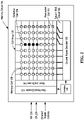
- Figure 2 illustrates another defect scenario that may occur in the memory circuit 100 according to one embodiment.
- defective cells 109 lie in a column of the cell array 120.
- the memory circuit 100 receives from a test circuit a repair address indicating the column containing the defective cells 109, the memory circuit 100 performs self-repair by disabling the defective column and enabling the redundant column.
- a re-mapping of column addresses is configured to replace the defective column with another column.
- the memory circuit includes a controller 130 to receive the repair address from the test circuit and to generate control signals accordingly to enable row repair or column repair, when memory self-repair is needed.
- the repair address is also referred to as a shared repair address, as it can be used to indicate either a row repair address or a column repair address.
- the memory circuit 100 also receives a row repair enable (RR_EN) signal and a column repair enable (CR_EN) signal from the test circuit.
- RR_EN row repair enable
- CR_EN column repair enable
- a row repair decoder 140 decodes the repair address to identify the defective row, and signals word line drivers 145 to replace the defective row with the redundant row.
- Each row of memory cells 106 is coupled to a word line driven by a corresponding word line driver 145.
- the corresponding word line driver 145 is disabled, and the word line driver 145 coupled to the redundant row is enabled.
- access to the defective row is re-routed to the redundant row.
- Figure 1 illustrates an example in which the 7 th row from the top is disabled and access to the 7 th row is re-routed or re-mapped to the redundant row.
- each multiplexer may be set to a default state (indicated by a straight line) or a "shifted state" (indicated by a bent line as shown in Figure 2 ).
- a multiplexer in the default state connects a memory I/O port to a data line of regular cells in the same column.
- a multiplexer in the shifted state connects a memory I/O port to a data line in the next column.
- the column repair decoder 150 decodes the repair address to identify the defective column, and signals the column shift circuit 155 to change the setting of its multiplexers starting from the defective column.
- Figure 2 illustrates an example in which the 6 th column from the left (as shown in the example) is found to contain defective cells.
- the column shift circuit 155 sets the multiplexers of the 6 th , 7 th , and 8 th columns to the shifted state. That is, these multiplexers are configured to select their respective next columns, which are the 7 th column, the 8 th column, and the redundant column, respectively.
- the redundant column is selected to replace the last column of regular cells.
- the mapping between the memory I/O ports and the data lines is shifted by one column for those columns with column addresses (i.e., column indices) equal to or higher than that of the defective column. In this example, access to the rows remains unchanged.
- Figure 3 illustrates a system 300 including the memory circuit 100 ( Figures 1 and 2 ) and a test circuit according to one embodiment.
- a non-limiting example of the test circuit is an MBIST circuit 310.
- the system 300 maybe part of an SOC.
- the MBIST circuit 310 sends test patterns to the memory circuit 100 via an interface circuit 350. From the output of the memory circuit 100, the MBIST circuit 310 determines a repair signature, such as the repair address of a row or a column.
- the repair signature is loaded into a fuse register 320 to test whether the memory circuit 100 is repairable. If it is confirmed that the memory circuit 100 can be repaired by the repair signature, the repair signature is burned into a fuse memory, such as an electronic fuse (EFUSE) 330.
- An EFUSE controller 340 controls the access to the EFUSE 330. On a chip reset, the EFUSE controller 340 reads out the content of the EFUSE 330, which is then loaded into the fuse register 320 and sent to the memory circuit 100.
- the memory circuit 100 is coupled to a fuse bus 360 that includes wires (indicated by the wires in a dotted circle) to carry RR_EN, CR_EN, and a repair address.
- the wires of the fuse bus 360 connect to a set of fuse pins 370 of the memory circuit 100 (only one is labeled for simplicity). It is understood that the memory circuit 100 includes additional pins (not shown) for receiving signals from the MBIST circuit 310, the interface circuit 350, and other circuits.
- the shared repair address according to the disclosure reduces not only the wiring footprint of the fuse bus 360 coupled to the memory circuit 100, but also the routing areas taken by the wires represented by double-ended arrows in Figure 3 .
- the fuse bus 360 provides flexibility with only one additional enable signal.
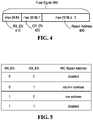
- Figure 4 illustrates an example of a fuse signal 400 according to one embodiment.
- the fuse signal 400 is received by the memory circuit 100 through the fuse pins 370 of Figure 3 .
- the fuse signal 400 includes a total of (max(M,N)+1) bits.
- the fuse signal 400 may include a first bit indicating RR_EN 410, a second bit indicating CR_EN 420, and the remaining bits (max(M,N)-2 : 0) indicating a repair address 430 of either a row or a column.
- the number of fuse pins used for the repair address 430 is equal to the greater of the row address width ((M-1) bits) and the column address width ((N-1) bits) for addressing a row and a column, respectively, in a cell array.
- Each bit of the fuse signal 400 is carried by a wire of the fuse bus 360 and received by the memory circuit 100 through a corresponding fuse pin 370.
- the number of fuse pins 370 and fuse bus 360 wires can be significantly reduced when compared with having both repair addresses for rows and columns at the same time.
- Figure 5 illustrates logics for determining row repair or column repair according to one embodiment.
- both CR_EN and RR_EN are de-asserted (e.g., logic low as represented by 0)
- both the row repair and the column repair are disabled. That is, no self-repair is performed.
- both CR_EN and RR_EN are asserted (e.g., logic high as represented by 1)
- both the row repair and the column repair are disabled. That is, no self-repair is performed.
- RR_EN is de-asserted and CR_EN is asserted
- row repair is disabled and column repair is enabled. That is, the repair address indicates a defective column address.
- RR_EN is asserted and CR_EN is de-asserted
- row repair is enabled and column repair is disabled. That is, the repair address indicates a defective row address.
- Figure 6 illustrates further details of the memory circuit 100 according to one embodiment. Components that are the same as those in Figures 1 and 2 are labeled with the same numerals.
- the controller 130 in the memory circuit 100 receives the fuse signal 400 ( Figure 4 ).
- the controller 130 may apply the logic shown in Figure 5 to the fuse signal 400 to determine whether a row repair or a column repair is to be performed.
- the controller 130 then passes the repair address to either the row repair decoder 140 or the column repair decoder 150 according to the determination.
- the controller 630 does not forward the fuse signal 400 when both RR_EN and CR_EN are asserted or de-asserted.
- both the row repair decoder 140 and the column repair decoder 150 may receive the fuse signal 400 and apply the logic shown in Figure 5 to determine whether a row repair or a column repair is to be performed.
- the row repair decoder 140 when the row repair decoder 140 receives a repair address for row repair, the row repair decoder 140 configures a mapping of the repair address to the redundant row.
- the repair address in this case is the defective row address.
- the row repair decoder 140 maps the defective row address to the redundant row.
- the column repair decoder 150 when the column repair decoder 150 receives a repair address for column repair, the column repair decoder 150 generates a shift control signal to set each multiplexer 652 in the column shift circuit 155 to either the default state or the shifted state as described before in connection with Figures 1 and 2 .
- the repair address in this case is the defective column address.
- Figure 7 is a flow diagram illustrating a method 700 for self-repair of a memory circuit according to one embodiment.
- Method 700 may be performed by a memory circuit, such as the memory circuit 100 in Figures 1 , 2 , and 6 .
- the memory circuit has fuse pins and a fuse bus shared by row repair and column repair.
- the memory circuit receives an input indicating row repair or column repair, and a repair address shared by the row repair and the column repair of a cell array.
- the cell array includes multiple rows and multiple columns of memory cells.
- the memory circuit maps the repair address of a defective row to a redundant row when the input indicates the row repair.
- the memory circuit maps the repair address of a defective column to another column when the input indicates the column repair.
Landscapes
- Engineering & Computer Science (AREA)
- Theoretical Computer Science (AREA)
- Human Computer Interaction (AREA)
- Physics & Mathematics (AREA)
- General Engineering & Computer Science (AREA)
- General Physics & Mathematics (AREA)
- For Increasing The Reliability Of Semiconductor Memories (AREA)
- Computer Security & Cryptography (AREA)
- Techniques For Improving Reliability Of Storages (AREA)
- Static Random-Access Memory (AREA)
Abstract
Description
- This application claims the benefit of
U.S. Provisional Application No. 63/120,272 filed on December 2, 2020 - The invention relates to a memory circuit that is reconfigurable to replace defective memory cells with redundant memory cells.
- Memory circuits are prone to faults that may occur during the fabrication process. For example, process variation may be one of the factors that cause defects in memory cells. A defective memory cell may be unable to hold its content, unstable with respect to memory operations, or cannot be accessed. Defective memory cells may be distributed randomly and along any direction on a chip. Memory defects adversely impact the total chip yield.
- One solution for the defective memory problem is to add redundant memory cells to the memory. Typically, a memory test is conducted to identify faulty regions in the memory. The memory can be tested by external test hardware or by on-chip dedicated hardware. For example, a system-on-a-chip (SOC) platform may include a memory cell array coupled to a memory built-in self-test (MBIST) circuit. The MBIST circuit generates test patterns, identifies faulty memory regions from test results, and outputs repair signals to the memory. The memory is then reconfigured to replace defective memory cells with redundant memory cells within certain limits.
- A random-access memory (RAM) with redundant memory cells and reconfiguration circuitry is called a repairable RAM. A higher degree of redundancy typically means more memory cells can be repaired. However, the redundancy not only increases the memory cell area, but also increases wires and pins that route the repair signals to the memory.
- Therefore, there is a need for a memory repair mechanism that can provide a needed repair coverage with minimal overhead.
- A memory circuit, a system operative to perform self-repair, and a method for self-repair of a memory circuit according to the invention are defined in the independent claims. The dependent claims define preferred embodiments thereof. In one embodiment, a memory circuit is provided to perform self-repair. The memory circuit includes a cell array, a controller, a row repair decoder, and a column repair decoder. The cell array includes multiple rows and multiple columns of memory cells. The controller receives an input indicating row repair or column repair, and a repair address shared by the row repair and the column repair of the cell array. The row repair decoder maps the repair address of a defective row to a redundant row of the cell array when the input indicates the row repair. The column repair decoder maps the repair address of a defective column to another column of the cell array when the input indicates the column repair.
- In another embodiment, a system is provided to perform self-repair. The system includes a test circuit to generate test patterns and to identify defective memory cells. The system further includes a memory circuit coupled to the test circuit. The memory circuit includes a cell array, a controller, a row repair decoder, and a column repair decoder. The cell array includes multiple rows and multiple columns of memory cells. The controller receives an input indicating row repair or column repair, and a repair address shared by the row repair and the column repair of the cell array. The row repair decoder maps the repair address of a defective row to a redundant row of the cell array when the input indicates the row repair. The column repair decoder maps the repair address of a defective column to another column of the cell array when the input indicates the column repair.
- In yet another embodiment, a method is provided for self-repairing a memory circuit. The method includes the step of receiving an input indicating row repair or column repair, and a repair address shared by the row repair and the column repair of a cell array. The cell array includes multiple rows and multiple columns of memory cells. The method further includes the steps of mapping the repair address of a defective row to a redundant row of the cell array when the input indicates the row repair; and mapping the repair address of a defective column to another column when the input indicates the column repair.
- Advantages of the invention will be explained in detail in the following description.
- The invention is illustrated by way of example, and not by way of limitation, in the figures of the accompanying drawings in which like references indicate similar elements. It should be noted that different references to "an" or "one" embodiment in this disclosure are not necessarily to the same embodiment, and such references mean at least one. Further, when a particular feature, structure, or characteristic is described in connection with an embodiment, it is submitted that it is within the knowledge of one skilled in the art to effect such feature, structure, or characteristic in connection with other embodiments whether or not explicitly described.
-
Figure 1 illustrates a defect scenario that may occur in a memory circuit according to one embodiment. -
Figure 2 illustrates another defect scenario that may occur in a memory circuit according to one embodiment. -
Figure 3 illustrates a system including a memory circuit and a test circuit according to one embodiment. -
Figure 4 illustrates an example of a fuse signal according to one embodiment. -
Figure 5 illustrates logics for determining row repair or column repair according to one embodiment. -
Figure 6 illustrates a memory circuit that performs self-repair according to one embodiment. -
Figure 7 is a flow diagram illustrating a method for self-repair of a memory circuit according to one embodiment. - In the following description, numerous specific details are set forth. However, it is understood that embodiments of the invention may be practiced without these specific details. In other instances, well-known circuits, structures, and techniques have not been shown in detail in order not to obscure the understanding of this description. It will be appreciated, however, by one skilled in the art, that the invention may be practiced without such specific details. Those of ordinary skill in the art, with the included descriptions, will be able to implement appropriate functionality without undue experimentation.
- Embodiments of the invention provide a memory circuit coupled to a shared fuse bus that carries repair information of a row or a column. The memory circuit can perform self-repair according to the repair information. The memory circuit may be any type of random-access memory (RAM); a non-limiting example is a static RAM (SRAM) circuit. Preferably, the memory circuit includes a cell array organized in multiple rows and multiple columns, including a redundant row and a redundant column. The fuse bus is shared between row repair and column repair; more specifically, the repair information carried on the fuse bus indicates either row repair or column repair. Memory repair is made by replacing a defective row or column with a working row or column as will be described in detail below.
- In one embodiment, the memory circuit may be part of an SOC, and may be coupled to an on-chip test circuit (e.g., an MBIST circuit) via the fuse bus. The memory circuit may be coupled to the fuse bus through a set of fuse pins. The test circuit generates tests patterns and identifies defective memory cells. The test circuit then sends a fuse signal via the fuse bus to the memory circuit indicating the faulty memory region. The defective memory cells may extend along the row dimension or the column dimension of the memory cell array. The test circuit informs the memory circuit of row or column repair using the fuse bus. The memory circuit then self-repairs the defects in the identified row or column using the row or column redundancy.
- According to embodiments of the invention, the memory circuit may switch between multiple types of repairs (e.g., row repair and column repair) depending on the fault pattern. This on-demand switch between row and column is more flexible than a one-dimensional (1-D) design where the reparability of either a row or a column is fixed in hardware. The flexibility in the repair types (e.g., row or column) improves the repair coverage of the memory and increases the overall chip yield.
- Moreover, flexibility is achieved with negligible overhead because of the shared fuse bus and the shared fuse pins. Sharing a common set of fuse bus and fuse pins between rows and columns significantly reduces the wiring footprint (e.g., the number of pins and wires for routing the fuse signal) as compared with a two-dimensional (2-D) design. A 2-D design can repair both a row and a column at the same time, but requires much larger routing areas to accommodate two separate sets of fuse buses and pins for row repair and column repair.
- In the following description, the terms "connect," "couple" and their derivatives, are used to indicate that two or more elements, which may or may not be in direct physical contact, have an electrical connection between or among them. Thus, the terms "connected" and "coupled" hereinafter are used equivalently to "electrically connected" and "electrically coupled," respectively.
-
Figure 1 illustrates a defect scenario that may occur in amemory circuit 100 according to one embodiment. Thememory circuit 100 includes acell array 120, which further includesmemory cells 106 arranged in multiple rows and multiple columns. Thecell array 120 may include any number of multiple rows and any number of multiple columns. Eachmemory cell 106 is located at the intersection of a word line (represented by a horizontal line) and a data line (represented by a vertical line). Thecell array 120 includes a redundant row and a redundant column. Memory cells in the redundant row and the redundant column are referred to asredundant cells 107. Eachredundant cell 107 is represented inFigure 1 by a square filled with a slanting-line pattern. In this disclosure, thememory cells 106 that are not in the redundant row and column are referred to as "regular cells." It is understood that a redundant cell has the same structure and function as a regular cell. Each column of regular cells is connected to a memory I/O port. Thus, access to the columns is also referred to as I/O access. - The
cell array 120 may be tested for defects by the chip manufacturer.Figure 1 shows one defect scenario wheredefective cells 108 lie in a row. Eachdefective cell 108 is represented inFigure 1 by a darkened square. When thememory circuit 100 receives from a test circuit (not shown) a repair address indicating the row containing thedefective cells 108, thememory circuit 100 performs self-repair by disabling the defective row and enabling the redundant row. A re-mapping of row addresses is configured to replace the defective row with the redundant row. -
Figure 2 illustrates another defect scenario that may occur in thememory circuit 100 according to one embodiment. In this defect scenario, defective cells 109 lie in a column of thecell array 120. When thememory circuit 100 receives from a test circuit a repair address indicating the column containing the defective cells 109, thememory circuit 100 performs self-repair by disabling the defective column and enabling the redundant column. A re-mapping of column addresses is configured to replace the defective column with another column. - Preferably, the memory circuit includes a
controller 130 to receive the repair address from the test circuit and to generate control signals accordingly to enable row repair or column repair, when memory self-repair is needed. The repair address is also referred to as a shared repair address, as it can be used to indicate either a row repair address or a column repair address. - In addition to the repair address, the
memory circuit 100 also receives a row repair enable (RR_EN) signal and a column repair enable (CR_EN) signal from the test circuit. When only RR_EN is asserted, arow repair decoder 140 decodes the repair address to identify the defective row, and signalsword line drivers 145 to replace the defective row with the redundant row. Each row ofmemory cells 106 is coupled to a word line driven by a correspondingword line driver 145. When one or more memory cells in a given row are found to be defective, the correspondingword line driver 145 is disabled, and theword line driver 145 coupled to the redundant row is enabled. Furthermore, access to the defective row is re-routed to the redundant row.Figure 1 illustrates an example in which the 7th row from the top is disabled and access to the 7th row is re-routed or re-mapped to the redundant row. - In the example of
Figure 1 , access to the columns (i.e., I/O access) remains unchanged. This is indicated by the straight lines in acolumn shift circuit 155, which may include a multiplexer for each column of regular cells (i.e., each column of memory cells not including the redundant column). According to the output of acolumn repair decoder 150, each multiplexer may be set to a default state (indicated by a straight line) or a "shifted state" (indicated by a bent line as shown inFigure 2 ). A multiplexer in the default state connects a memory I/O port to a data line of regular cells in the same column. A multiplexer in the shifted state connects a memory I/O port to a data line in the next column. When all of the multiplexers are set to the default state, the redundant column is unused. - Referring to
Figure 2 , when only CR_EN is asserted, thecolumn repair decoder 150 decodes the repair address to identify the defective column, and signals thecolumn shift circuit 155 to change the setting of its multiplexers starting from the defective column.Figure 2 illustrates an example in which the 6th column from the left (as shown in the example) is found to contain defective cells. Thecolumn shift circuit 155 sets the multiplexers of the 6th, 7th, and 8th columns to the shifted state. That is, these multiplexers are configured to select their respective next columns, which are the 7th column, the 8th column, and the redundant column, respectively. The redundant column is selected to replace the last column of regular cells. Thus, the mapping between the memory I/O ports and the data lines is shifted by one column for those columns with column addresses (i.e., column indices) equal to or higher than that of the defective column. In this example, access to the rows remains unchanged. -
Figure 3 illustrates asystem 300 including the memory circuit 100 (Figures 1 and2 ) and a test circuit according to one embodiment. A non-limiting example of the test circuit is anMBIST circuit 310. In one embodiment, thesystem 300 maybe part of an SOC. TheMBIST circuit 310 sends test patterns to thememory circuit 100 via aninterface circuit 350. From the output of thememory circuit 100, theMBIST circuit 310 determines a repair signature, such as the repair address of a row or a column. The repair signature is loaded into a fuse register 320 to test whether thememory circuit 100 is repairable. If it is confirmed that thememory circuit 100 can be repaired by the repair signature, the repair signature is burned into a fuse memory, such as an electronic fuse (EFUSE) 330. An EFUSE controller 340 controls the access to theEFUSE 330. On a chip reset, the EFUSE controller 340 reads out the content of theEFUSE 330, which is then loaded into the fuse register 320 and sent to thememory circuit 100. - The
memory circuit 100 is coupled to a fuse bus 360 that includes wires (indicated by the wires in a dotted circle) to carry RR_EN, CR_EN, and a repair address. The wires of the fuse bus 360 connect to a set of fuse pins 370 of the memory circuit 100 (only one is labeled for simplicity). It is understood that thememory circuit 100 includes additional pins (not shown) for receiving signals from theMBIST circuit 310, theinterface circuit 350, and other circuits. Compared with a 2-D design (where both a row and a column can be repaired at the same time), the shared repair address according to the disclosure reduces not only the wiring footprint of the fuse bus 360 coupled to thememory circuit 100, but also the routing areas taken by the wires represented by double-ended arrows inFigure 3 . Compared with a 1-D design (where the reparability of a row or a column is fixed in hardware), the fuse bus 360 provides flexibility with only one additional enable signal. -
Figure 4 illustrates an example of a fuse signal 400 according to one embodiment. The fuse signal 400 is received by thememory circuit 100 through the fuse pins 370 ofFigure 3 . For a cell array with M rows (including one redundant row) and N columns (including one redundant column), the fuse signal 400 includes a total of (max(M,N)+1) bits. For example, the fuse signal 400 may include a firstbit indicating RR_EN 410, a secondbit indicating CR_EN 420, and the remaining bits (max(M,N)-2 : 0) indicating arepair address 430 of either a row or a column. That is, the number of fuse pins used for therepair address 430 is equal to the greater of the row address width ((M-1) bits) and the column address width ((N-1) bits) for addressing a row and a column, respectively, in a cell array. Each bit of the fuse signal 400 is carried by a wire of the fuse bus 360 and received by thememory circuit 100 through a corresponding fuse pin 370. By using a shared repair address, the number of fuse pins 370 and fuse bus 360 wires can be significantly reduced when compared with having both repair addresses for rows and columns at the same time. -
Figure 5 illustrates logics for determining row repair or column repair according to one embodiment. When both CR_EN and RR_EN are de-asserted (e.g., logic low as represented by 0), both the row repair and the column repair are disabled. That is, no self-repair is performed. Similarly, when both CR_EN and RR_EN are asserted (e.g., logic high as represented by 1), both the row repair and the column repair are disabled. That is, no self-repair is performed. When RR_EN is de-asserted and CR_EN is asserted, row repair is disabled and column repair is enabled. That is, the repair address indicates a defective column address. When RR_EN is asserted and CR_EN is de-asserted, row repair is enabled and column repair is disabled. That is, the repair address indicates a defective row address. -
Figure 6 illustrates further details of thememory circuit 100 according to one embodiment. Components that are the same as those inFigures 1 and2 are labeled with the same numerals. Preferably, thecontroller 130 in thememory circuit 100 receives the fuse signal 400 (Figure 4 ). Thecontroller 130 may apply the logic shown inFigure 5 to the fuse signal 400 to determine whether a row repair or a column repair is to be performed. Thecontroller 130 then passes the repair address to either therow repair decoder 140 or thecolumn repair decoder 150 according to the determination. The controller 630 does not forward the fuse signal 400 when both RR_EN and CR_EN are asserted or de-asserted. Alternatively, both therow repair decoder 140 and thecolumn repair decoder 150 may receive the fuse signal 400 and apply the logic shown inFigure 5 to determine whether a row repair or a column repair is to be performed. - Preferably, when the
row repair decoder 140 receives a repair address for row repair, therow repair decoder 140 configures a mapping of the repair address to the redundant row. The repair address in this case is the defective row address. When thememory circuit 100 receives the defective row address for read or write operations, therow repair decoder 140 maps the defective row address to the redundant row. - Preferably, when the
column repair decoder 150 receives a repair address for column repair, thecolumn repair decoder 150 generates a shift control signal to set eachmultiplexer 652 in thecolumn shift circuit 155 to either the default state or the shifted state as described before in connection withFigures 1 and2 . The repair address in this case is the defective column address. -
Figure 7 is a flow diagram illustrating amethod 700 for self-repair of a memory circuit according to one embodiment.Method 700 may be performed by a memory circuit, such as thememory circuit 100 inFigures 1 ,2 , and6 . The memory circuit has fuse pins and a fuse bus shared by row repair and column repair. - At
step 710, the memory circuit receives an input indicating row repair or column repair, and a repair address shared by the row repair and the column repair of a cell array. The cell array includes multiple rows and multiple columns of memory cells. Atstep 720, the memory circuit maps the repair address of a defective row to a redundant row when the input indicates the row repair. Atstep 730, the memory circuit maps the repair address of a defective column to another column when the input indicates the column repair. - The operations of the flow diagram of
Figure 7 have been described with reference to the exemplary embodiments ofFigures 1 ,2 , and6 . However, it should be understood that the operations of the flow diagram ofFigure 7 can be performed by embodiments of the invention other than those discussed with reference toFigures 1 ,2 , and6 , and the embodiments discussed with reference toFigures 1 ,2 and6 can perform operations different than those discussed with reference to the flow diagram. While the flow diagram ofFigures 7 shows a particular order of operations performed by certain embodiments of the invention, it should be understood that such order is exemplary (e.g., alternative embodiments may perform the operations in a different order, combine certain operations, overlap certain operations, etc.). - While the invention has been described in terms of several embodiments, those skilled in the art will recognize that the invention is not limited to the embodiments described, and can be practiced with modification and alteration within the scope of the appended claims. The description is thus to be regarded as illustrative instead of limiting.
Claims (15)
- A memory circuit (100) operative to perform self-repair, comprising:a cell array (120) including a plurality of rows and a plurality of columns of memory cells (106);a controller (130) to receive an input indicating row repair or column repair, and a repair address shared by the row repair and the column repair of the cell array (120);a row repair decoder (140) to map the repair address of a defective row to a redundant row of the cell array (120) when the input indicates the row repair; anda column repair decoder (150) to map the repair address of a defective column to another column of the cell array (120) when the input indicates the column repair.
- The memory circuit (100) of claim 1, wherein the input includes one bit indicating row repair enable, in the following also referred to as RR_EN, another bit indicating column repair enable, in the following also referred to as CR_EN, and a set of bits indicating the repair address of either a row or a column.
- The memory circuit (100) of claim 2, wherein and the self-repair is performed when only one of the RR_EN and the CR_EN is asserted.
- The memory circuit (100) of any one of claims 1 to 3, further comprising:
a number of fuse pins (370) through which to receive the repair address, wherein the number is equal to the greater of a row address width and a column address width. - The memory circuit (100) of any one of claims 1 to 4, wherein the row repair decoder (140) is operative to replace a defective row with the redundant row, and the column repair decoder (150) is operative to shift the defective column and subsequent columns by one column.
- The memory circuit (100) of any one of claims 1 to 5, wherein the cell array (120) includes one redundant row and one redundant column of memory cells (106).
- A system (300) operative to perform self-repair, comprising:a test circuit (310) to generate test patterns and to identify defective memory cells (106); anda memory circuit (100) according to any one of claims 1 to 6, wherein the memory circuit (100) is coupled to the test circuit (310) and the controller (130) receives the input from the test circuit (310).
- The system (300) of claim 7, further comprising:
a fuse bus (360) to carry the input to the memory circuit (100), wherein the fuse bus (360) carries one-bit indicating row repair enable, in the following also referred to as RR_EN, another bit indicating column repair enable, in the following also referred to as CR_EN, and a set of bits indicating the repair address of either a row or a column. - The system (300) of claim 7 or 8, wherein the memory circuit (100) receives the repair address from the test circuit through the number of fuse pins (370).
- The system (300) of any one of claims 7 to 9, wherein the test circuit (310) is a memory built-in self-test, in the following also referred to as MBIST, circuit.
- A method for self-repair of a memory circuit, comprising:receiving an input indicating row repair or column repair, and a repair address shared by the row repair and the column repair of a cell array that includes a plurality of rows and a plurality of columns of memory cells (710);mapping the repair address of a defective row to a redundant row of the cell array when the input indicates the row repair (720); andmapping the repair address of a defective column to another column when the input indicates the column repair (730).
- The method of claim 11, wherein the input includes one bit indicating row repair enable, in the following also referred to as RR_EN, another bit indicating column repair enable, in the following also referred to as CR_EN, and a set of bits indicating the repair address of either a row or a column.
- The method of claim 12, wherein and the self-repair is performed when only one of the RR_EN and the CR_EN is asserted.
- The method of any one of claims 11 to 13, wherein the cell array includes one redundant row and one redundant column of memory cells.
- The memory circuit of any one of claims 1 to 6, the system of any one of claims 7 to 10, or the method of any one of claims 11 to 14, wherein the cell array (120) is a static random access memory, in the following also referred to as SRAM, cell array.
Applications Claiming Priority (2)
| Application Number | Priority Date | Filing Date | Title |
|---|---|---|---|
| US202063120272P | 2020-12-02 | 2020-12-02 | |
| US17/528,248 US11880607B2 (en) | 2020-12-02 | 2021-11-17 | Memory with fuse pins shared by multiple-type repairs |
Publications (1)
| Publication Number | Publication Date |
|---|---|
| EP4009327A1 true EP4009327A1 (en) | 2022-06-08 |
Family
ID=78806358
Family Applications (1)
| Application Number | Title | Priority Date | Filing Date |
|---|---|---|---|
| EP21210776.7A Pending EP4009327A1 (en) | 2020-12-02 | 2021-11-26 | Memory with fuse pins shared by multiple-type repairs |
Country Status (4)
| Country | Link |
|---|---|
| US (1) | US11880607B2 (en) |
| EP (1) | EP4009327A1 (en) |
| CN (1) | CN114596908A (en) |
| TW (1) | TWI777867B (en) |
Families Citing this family (1)
| Publication number | Priority date | Publication date | Assignee | Title |
|---|---|---|---|---|
| CN115881202B (en) * | 2023-02-09 | 2023-05-12 | 长鑫存储技术有限公司 | Repair circuit and method, memory and electronic equipment |
Citations (7)
| Publication number | Priority date | Publication date | Assignee | Title |
|---|---|---|---|---|
| US20020006064A1 (en) * | 1995-11-28 | 2002-01-17 | Mitsubishi Denki Kabushiki Kaisha | Semiconductor memory device and method of checking same for defect |
| US6507524B1 (en) * | 2000-11-30 | 2003-01-14 | Lsi Logic Corporation | Integrated circuit memory having column redundancy |
| US7216277B1 (en) * | 2003-11-18 | 2007-05-08 | Xilinx, Inc. | Self-repairing redundancy for memory blocks in programmable logic devices |
| US20100318843A1 (en) * | 2009-06-11 | 2010-12-16 | Stmicroelectronics Pvt., Ltd. | Shared fuse wrapper architecture for memory repair |
| US20120314520A1 (en) * | 2010-02-23 | 2012-12-13 | Rambus Inc. | Memory Architecture With Redundant Resources |
| US20130010538A1 (en) * | 1998-08-28 | 2013-01-10 | Mosaid Technologies Incorporated | Memory device and method for repairing a semiconductor memory |
| US10755799B1 (en) * | 2019-04-15 | 2020-08-25 | Micron Technology, Inc. | Apparatuses and methods for fuse latch redundancy |
Family Cites Families (9)
| Publication number | Priority date | Publication date | Assignee | Title |
|---|---|---|---|---|
| US5577050A (en) * | 1994-12-28 | 1996-11-19 | Lsi Logic Corporation | Method and apparatus for configurable build-in self-repairing of ASIC memories design |
| US5835425A (en) * | 1997-09-04 | 1998-11-10 | Siemens Aktiengesellschaft | Dimension programmable fusebanks and methods for making the same |
| JP2000348498A (en) * | 1999-06-08 | 2000-12-15 | Mitsubishi Electric Corp | Semiconductor test equipment |
| KR100327590B1 (en) * | 1999-10-20 | 2002-03-15 | 박종섭 | Fuse box for repairing memory device |
| US7734966B1 (en) * | 2002-12-26 | 2010-06-08 | Marvell International Ltd. | Method and system for memory testing and test data reporting during memory testing |
| US7116590B2 (en) * | 2004-08-23 | 2006-10-03 | Micron Technology, Inc. | Memory address repair without enable fuses |
| US7219275B2 (en) * | 2005-02-08 | 2007-05-15 | International Business Machines Corporation | Method and apparatus for providing flexible modular redundancy allocation for memory built in self test of SRAM with redundancy |
| KR20160148347A (en) * | 2015-06-16 | 2016-12-26 | 에스케이하이닉스 주식회사 | Self repair device and method |
| US10134483B2 (en) * | 2015-12-29 | 2018-11-20 | Texas Instruments Incorporated | Centralized built-in soft-repair architecture for integrated circuits with embedded memories |
-
2021
- 2021-11-17 US US17/528,248 patent/US11880607B2/en active Active
- 2021-11-19 CN CN202111402797.4A patent/CN114596908A/en not_active Withdrawn
- 2021-11-26 EP EP21210776.7A patent/EP4009327A1/en active Pending
- 2021-11-29 TW TW110144324A patent/TWI777867B/en active
Patent Citations (7)
| Publication number | Priority date | Publication date | Assignee | Title |
|---|---|---|---|---|
| US20020006064A1 (en) * | 1995-11-28 | 2002-01-17 | Mitsubishi Denki Kabushiki Kaisha | Semiconductor memory device and method of checking same for defect |
| US20130010538A1 (en) * | 1998-08-28 | 2013-01-10 | Mosaid Technologies Incorporated | Memory device and method for repairing a semiconductor memory |
| US6507524B1 (en) * | 2000-11-30 | 2003-01-14 | Lsi Logic Corporation | Integrated circuit memory having column redundancy |
| US7216277B1 (en) * | 2003-11-18 | 2007-05-08 | Xilinx, Inc. | Self-repairing redundancy for memory blocks in programmable logic devices |
| US20100318843A1 (en) * | 2009-06-11 | 2010-12-16 | Stmicroelectronics Pvt., Ltd. | Shared fuse wrapper architecture for memory repair |
| US20120314520A1 (en) * | 2010-02-23 | 2012-12-13 | Rambus Inc. | Memory Architecture With Redundant Resources |
| US10755799B1 (en) * | 2019-04-15 | 2020-08-25 | Micron Technology, Inc. | Apparatuses and methods for fuse latch redundancy |
Also Published As
| Publication number | Publication date |
|---|---|
| US20220171543A1 (en) | 2022-06-02 |
| CN114596908A (en) | 2022-06-07 |
| TW202223902A (en) | 2022-06-16 |
| TWI777867B (en) | 2022-09-11 |
| US11880607B2 (en) | 2024-01-23 |
Similar Documents
| Publication | Publication Date | Title |
|---|---|---|
| US6940765B2 (en) | Repair apparatus and method for semiconductor memory device to be selectively programmed for wafer-level test or post package test | |
| JP2588692B2 (en) | Redundant register programming method and column redundant integrated circuit | |
| KR100270005B1 (en) | Data processing system having memory sub-array redundancy and method therefor | |
| GB2129585A (en) | Memory system including a faulty rom array | |
| KR20020062206A (en) | Semiconductor storage device formed to optimize test technique and redundancy technology | |
| US6397349B2 (en) | Built-in self-test and self-repair methods and devices for computer memories comprising a reconfiguration memory device | |
| US6037799A (en) | Circuit and method for selecting a signal | |
| US8717838B1 (en) | Method and apparatus for memory redundancy | |
| US6552937B2 (en) | Memory device having programmable column segmentation to increase flexibility in bit repair | |
| US11880607B2 (en) | Memory with fuse pins shared by multiple-type repairs | |
| CN114333969A (en) | Memory controller with BISR logic circuit, operation method thereof and memory system | |
| US6055611A (en) | Method and apparatus for enabling redundant memory | |
| CN1954390B (en) | Repair of memory cells | |
| US20220277800A1 (en) | Memory system with redundant operation | |
| US6535436B2 (en) | Redundant circuit and method for replacing defective memory cells in a memory device | |
| US20040153732A1 (en) | Semiconductor memory device having a test circuit | |
| JPH0652697A (en) | Semiconductor memory with error correction function | |
| US5666312A (en) | Column redundancy scheme for a random access memory incorporating multiplexers and demultiplexers for replacing defective columns in any memory array | |
| JP2002025298A (en) | Integrated circuit | |
| JPH06203594A (en) | Semiconductor memory device | |
| US8289792B2 (en) | Memory test circuit, semiconductor integrated circuit and memory test method | |
| US20040184328A1 (en) | Semiconductor integrated circuit capable of testing with small scale circuit configuration | |
| GB2366890A (en) | Testing a memory with redundant cells | |
| KR100539296B1 (en) | Semiconductor Memory Arrays with Shared Column Redundancy | |
| KR100924579B1 (en) | Redundant memory cell access circuit, semiconductor memory device comprising same, and test method of semiconductor memory device |
Legal Events
| Date | Code | Title | Description |
|---|---|---|---|
| PUAI | Public reference made under article 153(3) epc to a published international application that has entered the european phase |
Free format text: ORIGINAL CODE: 0009012 |
|
| STAA | Information on the status of an ep patent application or granted ep patent |
Free format text: STATUS: THE APPLICATION HAS BEEN PUBLISHED |
|
| AK | Designated contracting states |
Kind code of ref document: A1 Designated state(s): AL AT BE BG CH CY CZ DE DK EE ES FI FR GB GR HR HU IE IS IT LI LT LU LV MC MK MT NL NO PL PT RO RS SE SI SK SM TR |
|
| STAA | Information on the status of an ep patent application or granted ep patent |
Free format text: STATUS: REQUEST FOR EXAMINATION WAS MADE |
|
| 17P | Request for examination filed |
Effective date: 20221201 |
|
| RBV | Designated contracting states (corrected) |
Designated state(s): AL AT BE BG CH CY CZ DE DK EE ES FI FR GB GR HR HU IE IS IT LI LT LU LV MC MK MT NL NO PL PT RO RS SE SI SK SM TR |
|
| P01 | Opt-out of the competence of the unified patent court (upc) registered |
Effective date: 20230627 |