EP4009326A1 - Data path interface circuit, memory and storage system - Google Patents
Data path interface circuit, memory and storage system Download PDFInfo
- Publication number
- EP4009326A1 EP4009326A1 EP21859353.1A EP21859353A EP4009326A1 EP 4009326 A1 EP4009326 A1 EP 4009326A1 EP 21859353 A EP21859353 A EP 21859353A EP 4009326 A1 EP4009326 A1 EP 4009326A1
- Authority
- EP
- European Patent Office
- Prior art keywords
- delay
- module
- memory
- data
- interface circuit
- Prior art date
- Legal status (The legal status is an assumption and is not a legal conclusion. Google has not performed a legal analysis and makes no representation as to the accuracy of the status listed.)
- Granted
Links
Images




Classifications
-
- G—PHYSICS
- G11—INFORMATION STORAGE
- G11C—STATIC STORES
- G11C11/00—Digital stores characterised by the use of particular electric or magnetic storage elements; Storage elements therefor
- G11C11/21—Digital stores characterised by the use of particular electric or magnetic storage elements; Storage elements therefor using electric elements
- G11C11/34—Digital stores characterised by the use of particular electric or magnetic storage elements; Storage elements therefor using electric elements using semiconductor devices
- G11C11/40—Digital stores characterised by the use of particular electric or magnetic storage elements; Storage elements therefor using electric elements using semiconductor devices using transistors
- G11C11/401—Digital stores characterised by the use of particular electric or magnetic storage elements; Storage elements therefor using electric elements using semiconductor devices using transistors forming cells needing refreshing or charge regeneration, i.e. dynamic cells
- G11C11/4063—Auxiliary circuits, e.g. for addressing, decoding, driving, writing, sensing or timing
- G11C11/407—Auxiliary circuits, e.g. for addressing, decoding, driving, writing, sensing or timing for memory cells of the field-effect type
- G11C11/409—Read-write [R-W] circuits
- G11C11/4093—Input/output [I/O] data interface arrangements, e.g. data buffers
-
- G—PHYSICS
- G11—INFORMATION STORAGE
- G11C—STATIC STORES
- G11C7/00—Arrangements for writing information into, or reading information out from, a digital store
- G11C7/22—Read-write [R-W] timing or clocking circuits; Read-write [R-W] control signal generators or management
-
- G—PHYSICS
- G06—COMPUTING OR CALCULATING; COUNTING
- G06F—ELECTRIC DIGITAL DATA PROCESSING
- G06F3/00—Input arrangements for transferring data to be processed into a form capable of being handled by the computer; Output arrangements for transferring data from processing unit to output unit, e.g. interface arrangements
- G06F3/06—Digital input from, or digital output to, record carriers, e.g. RAID, emulated record carriers or networked record carriers
-
- G—PHYSICS
- G06—COMPUTING OR CALCULATING; COUNTING
- G06F—ELECTRIC DIGITAL DATA PROCESSING
- G06F3/00—Input arrangements for transferring data to be processed into a form capable of being handled by the computer; Output arrangements for transferring data from processing unit to output unit, e.g. interface arrangements
- G06F3/06—Digital input from, or digital output to, record carriers, e.g. RAID, emulated record carriers or networked record carriers
- G06F3/0601—Interfaces specially adapted for storage systems
- G06F3/0602—Interfaces specially adapted for storage systems specifically adapted to achieve a particular effect
- G06F3/061—Improving I/O performance
- G06F3/0611—Improving I/O performance in relation to response time
-
- G—PHYSICS
- G06—COMPUTING OR CALCULATING; COUNTING
- G06F—ELECTRIC DIGITAL DATA PROCESSING
- G06F3/00—Input arrangements for transferring data to be processed into a form capable of being handled by the computer; Output arrangements for transferring data from processing unit to output unit, e.g. interface arrangements
- G06F3/06—Digital input from, or digital output to, record carriers, e.g. RAID, emulated record carriers or networked record carriers
- G06F3/0601—Interfaces specially adapted for storage systems
- G06F3/0628—Interfaces specially adapted for storage systems making use of a particular technique
- G06F3/0638—Organizing or formatting or addressing of data
- G06F3/064—Management of blocks
-
- G—PHYSICS
- G11—INFORMATION STORAGE
- G11C—STATIC STORES
- G11C11/00—Digital stores characterised by the use of particular electric or magnetic storage elements; Storage elements therefor
- G11C11/21—Digital stores characterised by the use of particular electric or magnetic storage elements; Storage elements therefor using electric elements
- G11C11/34—Digital stores characterised by the use of particular electric or magnetic storage elements; Storage elements therefor using electric elements using semiconductor devices
- G11C11/40—Digital stores characterised by the use of particular electric or magnetic storage elements; Storage elements therefor using electric elements using semiconductor devices using transistors
- G11C11/401—Digital stores characterised by the use of particular electric or magnetic storage elements; Storage elements therefor using electric elements using semiconductor devices using transistors forming cells needing refreshing or charge regeneration, i.e. dynamic cells
- G11C11/4063—Auxiliary circuits, e.g. for addressing, decoding, driving, writing, sensing or timing
-
- G—PHYSICS
- G11—INFORMATION STORAGE
- G11C—STATIC STORES
- G11C11/00—Digital stores characterised by the use of particular electric or magnetic storage elements; Storage elements therefor
- G11C11/21—Digital stores characterised by the use of particular electric or magnetic storage elements; Storage elements therefor using electric elements
- G11C11/34—Digital stores characterised by the use of particular electric or magnetic storage elements; Storage elements therefor using electric elements using semiconductor devices
- G11C11/40—Digital stores characterised by the use of particular electric or magnetic storage elements; Storage elements therefor using electric elements using semiconductor devices using transistors
- G11C11/401—Digital stores characterised by the use of particular electric or magnetic storage elements; Storage elements therefor using electric elements using semiconductor devices using transistors forming cells needing refreshing or charge regeneration, i.e. dynamic cells
- G11C11/4063—Auxiliary circuits, e.g. for addressing, decoding, driving, writing, sensing or timing
- G11C11/407—Auxiliary circuits, e.g. for addressing, decoding, driving, writing, sensing or timing for memory cells of the field-effect type
- G11C11/4076—Timing circuits
-
- G—PHYSICS
- G11—INFORMATION STORAGE
- G11C—STATIC STORES
- G11C16/00—Erasable programmable read-only memories
- G11C16/02—Erasable programmable read-only memories electrically programmable
- G11C16/06—Auxiliary circuits, e.g. for writing into memory
- G11C16/10—Programming or data input circuits
-
- G—PHYSICS
- G11—INFORMATION STORAGE
- G11C—STATIC STORES
- G11C29/00—Checking stores for correct operation ; Subsequent repair; Testing stores during standby or offline operation
- G11C29/02—Detection or location of defective auxiliary circuits, e.g. defective refresh counters
- G11C29/023—Detection or location of defective auxiliary circuits, e.g. defective refresh counters in clock generator or timing circuitry
-
- G—PHYSICS
- G11—INFORMATION STORAGE
- G11C—STATIC STORES
- G11C29/00—Checking stores for correct operation ; Subsequent repair; Testing stores during standby or offline operation
- G11C29/02—Detection or location of defective auxiliary circuits, e.g. defective refresh counters
- G11C29/028—Detection or location of defective auxiliary circuits, e.g. defective refresh counters with adaption or trimming of parameters
-
- G—PHYSICS
- G11—INFORMATION STORAGE
- G11C—STATIC STORES
- G11C7/00—Arrangements for writing information into, or reading information out from, a digital store
- G11C7/10—Input/output [I/O] data interface arrangements, e.g. I/O data control circuits, I/O data buffers
- G11C7/1051—Data output circuits, e.g. read-out amplifiers, data output buffers, data output registers, data output level conversion circuits
- G11C7/1066—Output synchronization
-
- G—PHYSICS
- G11—INFORMATION STORAGE
- G11C—STATIC STORES
- G11C7/00—Arrangements for writing information into, or reading information out from, a digital store
- G11C7/10—Input/output [I/O] data interface arrangements, e.g. I/O data control circuits, I/O data buffers
- G11C7/1078—Data input circuits, e.g. write amplifiers, data input buffers, data input registers, data input level conversion circuits
- G11C7/1093—Input synchronization
-
- G—PHYSICS
- G06—COMPUTING OR CALCULATING; COUNTING
- G06F—ELECTRIC DIGITAL DATA PROCESSING
- G06F13/00—Interconnection of, or transfer of information or other signals between, memories, input/output devices or central processing units
- G06F13/14—Handling requests for interconnection or transfer
- G06F13/16—Handling requests for interconnection or transfer for access to memory bus
- G06F13/1668—Details of memory controller
- G06F13/1689—Synchronisation and timing concerns
-
- G—PHYSICS
- G11—INFORMATION STORAGE
- G11C—STATIC STORES
- G11C2207/00—Indexing scheme relating to arrangements for writing information into, or reading information out from, a digital store
- G11C2207/22—Control and timing of internal memory operations
- G11C2207/2254—Calibration
-
- G—PHYSICS
- G11—INFORMATION STORAGE
- G11C—STATIC STORES
- G11C7/00—Arrangements for writing information into, or reading information out from, a digital store
- G11C7/10—Input/output [I/O] data interface arrangements, e.g. I/O data control circuits, I/O data buffers
- G11C7/1051—Data output circuits, e.g. read-out amplifiers, data output buffers, data output registers, data output level conversion circuits
- G11C7/1069—I/O lines read out arrangements
Definitions
- the present application relates to the field of integrated circuits, and more particularly, to a data path interface circuit, a memory and a memory system.
- a semiconductor memory is a memory that accesses through semiconductor circuits, and a Dynamic Random Access Memory (DRAM) is widely applied to various fields because of its high storage speed and high integration.
- DRAM Dynamic Random Access Memory
- Multiple memory blocks are generally arranged in the memory to achieve a greater memory space.
- data transmission speeds of the different memory blocks are different, which leads to timings of the different memory blocks are inconsistent, and transmission synchronization of stored data is not good.
- An aspect of the present application provides a data path interface circuit, which includes a writing path module, a reading path module, a first delay module and a delay control module.
- the writing path module is connected to an internal port and an external port respectively, and is configured to transmit stored data to the internal port from the external port.
- the reading path module is connected to the internal port and the external port respectively, and is configured to transmit the stored data to the external port from the internal port.
- the first delay module is connected to the external port and the internal port respectively, and is configured to obtain the stored data from the external port or the internal port, perform delay processing on the stored data, and transmit the delayed stored data to the writing path module and/or the reading path module.
- the delay control module is connected to the first delay module and is configured to receive a signal instruction from external and control delay time for the first delay module to perform the delay processing according to the signal instruction.
- Another aspect of the present application provides a memory, which includes the data path interface circuit, a data processing module and a memory block.
- the data processing module is connected to the external port of the data interface circuit, and is configured to process the stored data.
- the memory block is connected to the internal port of the data interface circuit, and is configured to store the stored data.
- Another aspect of the present application provides a memory system, which includes the memory, an electronic device and a processing module controller.
- the processing module controller is connected to the memory and the electronic device respectively, and is configured to enable a corresponding number of the data processing modules in the memory according to system information of the electronic device.
- orientation or position relationships indicated by terms “upper”, “lower”, “vertical”, “horizontal”, “inner”, “outer”, and the like are orientation or position relationships shown in the drawings, are adopted not to indicate or imply that indicated devices or components must be in specific orientations or structured and operated in specific orientations but only to conveniently describe the embodiments of the present application and simplify descriptions and thus should not be understood as limits to the embodiments of the present application.
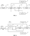
- FIG. 1 is a structural schematic diagram of a data path interface circuit 10 in a first embodiment.
- the data path interface circuit 10 includes a writing path module 100, a reading path module 200, a first delay module 300 and a delay control module 400.
- the data path interface circuit 10 is configured with an internal port 11 and an external port 12.
- the internal port 11 is configured to connect with a memory block 30 inside a memory, transmit stored data to be written to the memory block 30 or read the stored data from the memory block.
- the external port 12 is configured to receive the stored data to be written sent from an external electronic device or send the stored data read in the memory block 30 to the external electronic device.
- the writing path module 100 is connected to the internal port 11 and the external port 12 respectively, and is configured to transmit the stored data to the internal port 11 from the external port 12.
- An input end of the writing path module 100 is indirectly connected to the external port 12, specifically, the input end of the writing path module 100 is indirectly connected to the external port 12 through the first delay module 300, and an output end of the writing path module 100 is directly connected to the internal port 11. That is, the stored data to be written is input from the external electronic device, and reaches the memory block 30 through the external port 12, the first delay module 300, the writing path module 100 and the internal port 11 of the data path interface circuit, so that writing of the stored data is realized.
- the reading path module 200 is connected to the internal port 11 and the external port 12 respectively, and is configured to transmit the stored data to the external port 12 from the internal port 11.
- An input end of the reading path module 200 is indirectly connected to the internal port 11, specifically, the input end of the reading path module 200 is indirectly connected to the internal port 11 through the first delay module 300, and an output end of the reading path module 200 is directly connected to the external port 12. That is, the stored data is read from the memory block 30, and reaches the external electronic device through the internal port 11, the first delay module 300, the reading path module 200 and the external port 12 of the data path interface circuit, so that reading of the stored data is realized.
- the data path interface circuit 10 only executes one of writing operation and reading operation at the same time. As a result, the writing path module 100 and the reading path module 200 output the stored data in a time-sharing mode.
- the first delay module 300 is connected to the external port 12 and the internal port 11 respectively, and is configured to obtain the stored data from the external port 12 or the internal port 11, perform delay processing on the stored data, and transmit the delayed stored data to the writing path module 100 and/or the reading path module 200.
- the first delay module 300 obtains the stored data from the external port 11, performs delay processing on the stored data and transmits the delayed data to the writing path module 100.
- the stored data to be written are written from data pins of the memory.
- Each of the data pins is connected to multiple memory blocks 30, and is configured to transmit the stored data to the connected multiple memory blocks 30. It should be understood that length of transmission paths between the external port 12 of each data path interface circuit 10 and the data pins is not the same. As a result, even if the data reaches the data pins simultaneously, the stored data cannot reach each memory block 30 simultaneously based on similar data transmission speed and different lengths of the transmission paths.
- the first delay module 300 may perform delay processing on the received stored data for proper delay time, so that the stored data reaches the internal port 11 within a preset target time. In such a manner, the time that the stored data reaches the internal port 11 in each data path interface circuit 10 is the same or the time errors are within a bearable error range of the data path interface circuit 10, so that the unsynchronized transmission phenomenon of the stored data is solved.
- the first delay module 300 is configured with an output end.
- the output end is connected to a writing path module 100 and a reading path module 200 respectively.
- the first delay module 300 outputs the delayed stored data to the wiring path module 100 and the reading path module 200 simultaneously.
- one of the writing path module 100 and the reading path module 200 may be controlled to be enabled for outputting stored data.
- the first delay module 300 also may be configured with two output ends. The two output ends are respectively connected to a writing path module 100 and a reading path module 200 in a one-to-one correspondence. One of the two output ends of the first delay module 300 may be controlled to output stored data, so that only one of the writing path module 100 and the reading path module 200 may receive the stored data and output the stored data.
- a delay control module 400 is connected to the first delay module 300 and is configured to receive a signal instruction from external and control delay time for the first delay module 300 to perform the delay processing according to the signal instruction.
- the signal instruction is an instruction that is configured to indicate the data path interface circuit 10 to execute corresponding operation, for example, at least one of a write instruction, a read instruction or a mode selection coding instruction.
- the write instruction is configured to indicate the data path interface circuit 10 to execute corresponding writing operation.
- the delay control module 400 may be configured with one or more input ends, and may be configured to generate a control signal of the first delay module 300 according to a signal instruction from the input end. For example, if the delay control module 400 is configured with an input end, a control signal may be generated in response to one of the write instruction, the read instruction and the mode selection coding instruction. If the delay control module 400 is configured with two input ends, a control signal may be generated in response to two of the write instruction, the read instruction and the mode selection coding instruction. It should be understood that the more the types of signal instruction needed for the delay control module 400, the more complex the logistics of generating the control signal, and correspondingly the more reliable and comprehensive the control function. In such a manner, the reliability and the completeness of the data path interface circuit 10 may be improved, i.e., the transmission synchronization of the stored data is improved to a greater extent.
- the data path interface circuit 10 includes a writing path module 100, a reading path module 200, a first delay module 300 and a delay control module 400.
- the writing path module 100 is connected to an internal port 11 and an external port 12 respectively, and is configured to transmit stored data to the internal port 11 from the external port 12.
- the reading path module 200 is connected to the internal port 11 and the external port 12 respectively, and is configured to transmit the stored data to the external port 12 from the internal port 11.
- the first delay module 300 is connected to the external port 12 and the internal port 11 respectively, and is configured to obtain the stored data from the external port 12 or the internal port 11, perform delay processing on the stored data, and transmit the delayed stored data to the writing path module 100 and/or the reading path module 200.
- the delay control module 400 is connected to the first delay module 300 and is configured to receive a signal instruction from external and control delay time for the first delay module to perform the delay processing according to the signal instruction. Based on a control signal from the delay control module 400, the first delay module 300 may perform delay processing on the received stored data for proper delay time, so that the stored data reaches the internal port 11 or the external port 12 within a preset target time. In such a manner, the transmission time of the stored data in each data path interface circuit 10 between the internal port 11 and the external port 12 is the same, or transmission time errors are within a bearable error range of the data path interface circuit 10, so that the data path interface circuit 10 with better transmission synchronization on the stored data is realized.
- FIG. 2 is a schematic structural diagram of a data path interface circuit 10 in a second embodiment.
- the first delay module 300 includes a selection unit 310 and a temporary storage unit 320.
- a setting mode of the writing path module 100, the reading path module 200 and the delay control module 400 is the same with the setting mode in the embodiment in FIG. 1 , which is not detailed again herein.
- Input ends of the selection unit 310 are connected to the external port 12 and the internal port 11 respectively, and a control end of the selection unit 310 is configured to receive the signal instruction.
- the selection unit 310 is configured with two input ends, and the two input ends of the selection unit 310 are respectively connected to the internal port 11 and the external port 12 in a one-to-one correspondence to obtain stored data from the two ports respectively.
- the selection unit 310 is further configured with a control end, and the control end of the selection unit 310 is configured to receive a signal instruction to selectively output one of the received two stored data according to the signal instruction.
- the signal instruction may be a write instruction, so the selection unit 310 selectively outputs the stored data from the external port 12, so that writing of the data is realized.
- the selection unit 310 is a one-of-two multiplexer.
- the selection unit 310 also may be a one-of-three multiplexer and the like, that is, three input ends may be configured to realize a more complex selection function and transmission function.
- a data input end of the temporary storage unit 320 is connected to an output end of the selection unit 310, and a control end of the temporary storage unit 320 is connected to an output end of the delay control module 400.
- the temporary storage unit 320 includes at least one of a latch, a flip-flop or a register.
- a control end of the temporary storage unit 320 includes at least one of a clock drive end, a set end or a reset end.
- the temporary storage unit 320 may include a trigger, which is a D trigger.
- An input end of the D trigger is connected to the output end of the selection unit 310, the clock drive end of the D trigger is connected to the output end of the delay control module 400, and an output end of the D trigger is connected to the writing path module 100 and the reading path module 200 respectively.
- the D trigger samples a signal from the input end responsive to a control signal from the clock drive end.
- sampling time of the D trigger may be controlled, so that the stored data reaches the internal port 11 or the external port 12 within a target time through the writing path module 100 or the reading path module 200.
- a data path interface circuit 10 with better timing synchronization is realized.
- a preset enabling signal is output to the set end and/or the reset end, so that stable output of the temporary storage unit 320 may be ensured, and the reliability of the output signal of the data path interface circuit 10 is improved.
- the temporary storage unit 320 also may be other devices with signal temporary storage functions such as a JK trigger and a RS trigger.
- control signal includes at least one of a pulse signal, a signal rising edge or a signal falling edge. If the temporary storage unit 320 is a latch, it may be controlled through the pulse signal. If the temporary storage unit 320 is a flip-flop, it may be triggered through the signal rising edge or the signal falling edge. It should be understood that edge trigger may provide a greater timing margin, so as to improve the accuracy of sampling timing of the temporary storage unit 320, and then improve the reliability of the data path interface circuit 10.
- FIG. 3 is a schematic structural diagram of a data path interface circuit 10 in a third embodiment.
- the writing path module 100 includes a writing buffer unit 100
- the reading path module 200 includes a reading buffer unit 210.
- a setting mode of the selection unit 310, the temporary storage unit 320 and the delay control module 400 is the same with the setting mode in the embodiment in FIG. 2 , which is not detailed again herein.
- An input end of the writing buffer unit 110 is connected to an output end of the temporary storage unit 320, an output end of the writing buffer unit 100 is connected to the internal port 11, and a control end of the writing buffer unit 110 is configured to receive the signal instruction.
- the writing buffer unit 110 buffers and outputs the delayed stored data from the input end responsive to the signal instruction received at the control end, so that further adjustment of timing is realized to provide a writing path module 100 with better timing accuracy during writing of the stored data and a data path interface circuit 10.
- An input end of the reading buffer unit 210 is connected to an output end of the temporary storage unit 320, an output end of the reading buffer unit 210 is connected to the external port 12, and a control end of the reading buffer unit 210 is configured to receive the signal instruction. Similar to the writing buffer unit 110, the reading buffer unit 210 may be set to provide a reading path module 200 with better timing accuracy during reading of the stored data and a data path interface circuit 10.
- FIG. 4 is a schematic structural diagram of a data path interface circuit 10 in a fourth embodiment.
- the delay control module 400 includes a delay chain 410 and a control signal generation circuit 420.
- a setting mode of the selection unit 310, the temporary storage unit 320, the writing buffer unit 110 and the reading buffer unit 210 is the same with the setting mode in the embodiment in FIG. 3 , which is not detailed again herein.
- An input end of the delay chain 410 is configured to receive the signal instruction, and the delay chain is configured to delay and output the signal instruction.
- the delay chain 410 may be a fixed delay chain 410.
- the fixed delay chain 410 may include multiple transmission grates connected in series. Each of the transmission gates is configured with a fixed delay time. Thus, a corresponding number of transmission gates may be set according to the preset delay time needed for the delay chain 410, so that a target preset delay time is generated.
- the fixed delay chain 410 may include an even number of inverters connected in series. By setting the even number of inverters, it may be ensured that an output delay signal corresponds to an electric level state of the input signal instruction, and there is only a difference in timing. Similar to the fixed delay chain 410 consisting of the aforementioned transmission gates, a corresponding number of inverters may be set according to the preset delay time needed for the delay chain 410, so that a target preset delay time is generated.
- the delay chain 410 may be a programmable delay chain 410. It should be understood that properties such as signal transmission speed in the data path interface circuit 10 may change with a temperature and other conditions of use environment. As a result, if conditions of the use environment change, there will be a risk of timing abnormality and even transmitted signal error.
- condition changes of the use environment of the data path interface circuit 10 may be detected by the detection structure, and the delay time of the programmable delay chain 410 may be adjusted according to the detected results, so that timing errors are avoided and a data path interface circuit with better reliability is provided.
- the detection structure may be a sensor which detects the use environment, so as to adjust the delay time according to changes of the environment.
- the detection structure also may be a feedback circuit, i.e., the input is fed back according to the timing of the signal output from the data path interface circuit 10, so that accuracy of the timing is improved through a closed-loop adjustment.
- the programmable delay chain 410 may include multiple delay units. Each of the delay units is configured to generate delay with a set step length, and realize adjustment on the delay time through a coding group.
- the coding group includes multiple control coding bits which are in one-to-one correspondence to the delay units.
- the programmable delay chain 410 includes 8 delay units, and the coding group includes 8 control coding bits. When a value of the coding group is 10000000, a first delay unit is controlled to turn on and other delay units are controlled to turn off, so that a delay with a set step length is generated.
- the programmable delay chain 410 may be controlled by changing the value of the coding group. It should be noted that the examples are only used for description, and not used to limit the programmable delay chain 410 and the coding group specifically.
- control signal generation circuit 420 is connected to an output end of the delay chain 410, and an output end of the control signal generation circuit 420 is connected to the control end of the temporary storage unit 320.
- the control signal generation circuit 420 is configured to generate a control signal according to a signal output from the delay chain 410.
- the control signal from the control signal generation circuit 420 is a pulse signal, a signal rising edge or a signal falling edge
- the control signal may realize a more reliable timing control function on the temporary storage unit 320.
- the signal instruction and the delayed signal instruction may not certainly in an expected control signal form.
- a control signal which may be matched with the timing of the delayed signal instruction and is in a target form may be generated through the control signal generation circuit 420, so that accurate control on the temporary storage unit 320 is realized.
- the first delay module 300 and the delay control module 400 are configured with two operating modes.
- the two operating modes include a delay mode and a quick mode.
- the delay mode the first delay module 300 and the delay control module 400 are valid.
- the quick mode the delay control module 400 is invalid, and transmission delay on the stored data by the first delay module 300 is zero.
- the first delay module 300 and the delay control module 400 are valid, which means that a delay function of the first delay module 300 is enabled, and the delay control module 400 may delay the stored data correspondingly by generating a control signal according to the signal instruction.
- the first delay module 300 and the delay control module 400 are invalid, which means that the first delay module 300 only enables a transmission function of the stored data, and does not enable the delay function, so that the stored data pass through quickly, thereby increasing the operating speed of the data path interface circuit 10.
- the aforementioned "transmission delay is zero" means that the first delay module 300 does not set extra delay time for the stored data, but the wires and other structures in the first delay module 300 have a certain inherent delay. The delay time of the inherent delay is very short, i.e., the inherent delay may be ignored.
- FIG. 5 is a structural schematic diagram of a data path interface circuit 10 in a fifth embodiment.
- the data path interface circuit 10 further includes a mode selection module 500.
- the mode selection module 500 is connected to the first delay module 300 and the delay control module 400 respectively, and is configured to receive the signal instruction, and control the operating modes of the first delay module 300 and the delay control module 400 according to the signal instruction. It should be understood that path lengths of receiving the stored data by the each of memory blocks 30 are different for different operating modes and different positions of the memory blocks 30. Thus, the data path interface circuit 10 corresponding to the memory block 30 with the longest data transmission path is set as the quick mode, so that the stored data passes through with highest speed.
- Data path interface circuits 10 of other memory blocks 30 are set as the delay mode, and the data path interface circuit 10 corresponding to each memory block 30 is controlled to generate corresponding delay, so that sum of transmission time consumed of the stored data on a transmission path and delay time are a set value, so that data transmission time corresponding each of the memory blocks 30 is the same.
- the set value may be transmission time corresponding the longest data transmission path.
- FIG. 6 is a structural schematic diagram of a memory in an embodiment.
- the memory includes a data path interface circuit 10, a data processing module 20 and a memory block 30.
- the data path interface circuit 10 is connected to the data processing module 20 and the memory block 30 respectively, so that timing processing on the transmitted stored data is realized.
- the data processing module 20 is connected to the external port of the data interface circuit 10, and is configured to process the stored data.
- the processing on the stored data by the data processing module 20 may be serial/parallel converting for stored data transmission. It should be understood that the data processing module 20 may also execute other types of processing on the stored data to achieve the purpose of improving the transmission speed of the stored data and the like.
- the memory block 30 is connected to the internal port 11 of the data interface circuit 10, and is configured to store the stored data.
- the memory block 30 may include at least two memory sub blocks 31, which are connected to a same memory block control circuit.
- the control circuit includes at least one of a row decoding circuit, a column decoding circuit or a redundant circuit.
- the control circuit may be shared to reduce the number of wirings in the memory, so that integral integration of the memory is improved. It should be understood that the control complexity also may be improved by sharing the control circuit. A proper circuit may be selected to share according to practical wiring needs, so that balance between integration and control difficulty is realized.
- FIG. 6 shows multiple bidirectional drivers 40, which are arranged on a transmission path of stored data.
- the bidirectional drivers 40 in FIG. 6 are only used to schematically illustrate the length of the transmission path and data transmission speed. Specifically, it means that the data transmission path provided with the bidirectional drivers 40 is relatively long, and the data transmission speed is relatively slow.
- the bidirectional drivers shown in FIG. 6 are not used to limit the specific structure of the data transmission path in the embodiments of the present application.
- the bidirectional drivers 40 on each transmission path are not limited to the number and the set positions shown in FIG. 6 .
- the memory includes the multiple data path interface circuits 10 and the multiple memory blocks 30, and the data path interface circuits 10 and the memory blocks 30 are set in one-to-one correspondence.
- the external ports 12 of the multiple data path interface circuits 10 are connected to the same data processing module 20.
- the internal ports 11 of the data path interface circuits 10 are connected to the multiple memory sub blocks 31.
- Read stored data may reach the data processing module 20 from the memory sub blocks 31 through the internal ports 11 and the external ports 12 of the interface circuits, so that reading of the data is realized.
- the written-in stored data may reach the memory sub blocks 31 from the data processing module 20 through the external ports 12 and the internal ports 11 of the interface circuits, so that written-in of the data is realized.
- transmission time matching includes that the data transmission time corresponding to each of the memory sub blocks 31 is completely the same, and errors among the data transmission time corresponding to different memory sub blocks 31 are within an acceptable range, i.e., accuracy of the stored data is not affected.
- two data processing modules 20 are configured to adapt to electronic devices with different configurations.
- the data processing modules 20 are connected to the multiple data path interface circuits 10 respectively.
- the data processing module 20 is controlled to enable for transmitting data.
- a set number of the data processing modules 20 are controlled to enable for synchronously transmitting data to the different memory blocks 30.
- the memory is applied to a computer with a 64-bit system, computation speed and addressing ability of the computer are relatively strong, and therefore, the two data processing modules 20 may be enabled simultaneously to realize higher data transmission speed.
- the memory When the memory is applied to a computer with a 32-bit system, only one data processing module 20 may be enabled, so that the stored data are ensured to be stably and reliably transmitted.
- the memory in the embodiment may select to enable a corresponding number of the data processing modules according to an external electronic device, so that application flexibility and universality of the memory are improved.
- FIG. 7 is a schematic diagram showing a operating mode in which two data processing modules are valid in an embodiment.
- the embodiment of FIG. 7 takes the access to a memory sub block BOL and a memory sub block BOH as an example.
- a data transmission path 202 is longer, so that the stored data needs to pass through a data path interface circuit 10 with a highest speed and reaches to the second data processing module 20H at a far end through a bidirectional driver 40 between circuits of the two data processing modules 20.
- a data transmission path 201 is shorter, so that the stored data are delayed for a time in the data path interface circuit 10, and are output to the corresponding drivers according to a direction of reading-writing operation.
- the delay time of the interface circuit is configured to match the bidirectional driver 40 in the middle and the length of the corresponding transmission path.
- data timings corresponding to the two memory sub blocks 31 may be kept consistent.
- An adjusting way for the delay time of other memory blocks 30 is the same with the adjusting way of the memory sub block BOL and the memory sub block B0H, which is not detailed again herein.
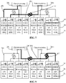
- FIG. 8 to FIG. 11 show a schematic diagram of a operating mode in which one data processing module 20 is valid of four embodiments.
- the access to a memory sub block B0L, a memory sub block B0H, a memory sub block B3L and a memory sub block B3H is taken as an example respectively to illuminate for a operating mode in which one data processing module 20 is valid.
- the longest transmission path is a data transmission path 203 (in black bold) from the first data processing module 20L to the memory sub block B3H.
- the data transmission path 203 is named as a timing datum path herein.
- the timing datum path includes wirings and the data path interface circuit 10.
- one bidirectional driver 40 and part of wirings are reduced on the data transmission path during access to the memory sub block B3L, and the transmission path is as shown in 204 in FIG. 9 (in black bold).
- a delay time circuit in the data path interface circuit 10 of the memory sub block B3L is operating, and the delay time is set to be matched with extra bidirectional driver 40 and related wirings on the data transmission path of the memory sub block B3H.
- delay time generated by the delay time circuit in the data path interface circuit 10 is limited if access to the memory sub block BOL and the memory sub block BOH is reading operation.
- a signal instruction for the memory sub block BOL and the memory sub block BOH needs to be delayed for the delay time, and then sends to the memory sub block BOL and the memory sub block BOH respectively.
- the delay time may be matched with delay time introduced through the middle bidirectional driver 40 on the data transmission path of the memory sub block B3L and the memory sub block B3H.
- a transmission path from the data processing module 20L to the memory sub block BOH is denoted by 205 in FIG. 10 (in black bold).
- a transmission path from the data processing module 20L to the memory sub block BOL is denoted by 201 in FIG. 11 (in black bold).
- FIG. 12 is a structural schematic diagram of a memory in another embodiment.
- FIG. 12 is a simplified drawing only showing a memory sub block BOL and a memory sub block B0H.
- the memory further includes a second delay module 50.
- the second delay module 50 may generate memory block control signal delay on the memory sub block BOL and the memory sub block BOH to further match with the delay time on the transmission path.
- the second delay module 50 is connected to a memory block 30, and is configured to receive the signal instruction and generate a control signal for the memory block 30 according to the signal instruction.
- the control signal of the memory block 30 is configured to control time when the stored data enters the memory block 30.
- the delay time generated on the memory block control signal by the second delay module 50 is matched with the delay time generated on the stored data by the data path interface circuit 10.
- the first delay module 300 and the second delay module 50 act simultaneously, so that transmission synchronization of the stored data among multiple memory sub blocks 31 may be further improved.
- delay time of the timing datum path 203 is recorded as T1
- delay time on wirings of the transmission path 204 is recorded as T2A
- delay time on the data path interface circuit 10 of the transmission path 204 is recorded as T2B
- delay time on wirings of the transmission path 205 is recorded as T3A
- delay time on the data path interface circuit 10 of the transmission path 205 is recorded as T3B
- delay time on wirings of the transmission path 201 in FIG.
- T4A delay time on the data path interface circuit 10 of the transmission path 201 (in FIG. 11 ) is recorded as T4B
- T4C delay time that the signal instruction passes through the second delay module 50 to generate the memory block control signal
- the embodiments of the present application further provide a memory system, which includes the memory such as above, an electronic device and a processing module controller.
- the processing module controller is connected to the memory and the electronic device respectively, and is configured to enable a corresponding number of the data processing modules in the memory according to system information of the electronic device.
- a memory system with higher stored data transmission synchronization is realized through the above structure.
- the specific setting mode of the memory may be referred to the above illustration, which is not detailed again herein
Landscapes
- Engineering & Computer Science (AREA)
- Theoretical Computer Science (AREA)
- Physics & Mathematics (AREA)
- General Engineering & Computer Science (AREA)
- General Physics & Mathematics (AREA)
- Computer Hardware Design (AREA)
- Microelectronics & Electronic Packaging (AREA)
- Human Computer Interaction (AREA)
- Memory System (AREA)
- Information Transfer Systems (AREA)
- Dram (AREA)
- Communication Control (AREA)
- Static Random-Access Memory (AREA)
Abstract
Description
- This application claims priority to
Chinese Patent Application No. 202011006722.X filed on September 23, 2020 - The present application relates to the field of integrated circuits, and more particularly, to a data path interface circuit, a memory and a memory system.
- A semiconductor memory is a memory that accesses through semiconductor circuits, and a Dynamic Random Access Memory (DRAM) is widely applied to various fields because of its high storage speed and high integration. Multiple memory blocks are generally arranged in the memory to achieve a greater memory space. However, when the current memory is running, data transmission speeds of the different memory blocks are different, which leads to timings of the different memory blocks are inconsistent, and transmission synchronization of stored data is not good.
- An aspect of the present application provides a data path interface circuit, which includes a writing path module, a reading path module, a first delay module and a delay control module.
- The writing path module is connected to an internal port and an external port respectively, and is configured to transmit stored data to the internal port from the external port.
- The reading path module is connected to the internal port and the external port respectively, and is configured to transmit the stored data to the external port from the internal port.
- The first delay module is connected to the external port and the internal port respectively, and is configured to obtain the stored data from the external port or the internal port, perform delay processing on the stored data, and transmit the delayed stored data to the writing path module and/or the reading path module.
- The delay control module is connected to the first delay module and is configured to receive a signal instruction from external and control delay time for the first delay module to perform the delay processing according to the signal instruction.
- Another aspect of the present application provides a memory, which includes the data path interface circuit, a data processing module and a memory block.
- The data processing module is connected to the external port of the data interface circuit, and is configured to process the stored data.
- The memory block is connected to the internal port of the data interface circuit, and is configured to store the stored data.
- Another aspect of the present application provides a memory system, which includes the memory, an electronic device and a processing module controller.
- The processing module controller is connected to the memory and the electronic device respectively, and is configured to enable a corresponding number of the data processing modules in the memory according to system information of the electronic device.
- Details of each of the embodiments of the disclosure are set forth in the following drawings and description. According to the record in the specification, the drawings and the claims, a person skilled in the art will easily understand other features, problems to be solved and advantageous effects of the disclosure.
- One or more drawings may be refereed for a better description and illustration of the embodiments of the present application, but additional details or examples for describing the drawings should not be considered as limiting to any one of the disclosure, the described embodiments or preferred embodiments of the present application.
-
FIG. 1 is a structural schematic diagram of a data path interface circuit in a first embodiment. -
FIG. 2 is a structural schematic diagram of a data path interface circuit in a second embodiment. -
FIG. 3 is a structural schematic diagram of a data path interface circuit in a third embodiment. -
FIG. 4 is a structural schematic diagram of a data path interface circuit in a fourth embodiment. -
FIG. 5 is a structural schematic diagram of a data path interface circuit in a fifth embodiment. -
FIG. 6 is a structural schematic diagram of a memory in an embodiment. -
FIG. 7 is a schematic diagram showing a operating mode in which two data processing modules are valid in an embodiment. -
FIG. 8 is a schematic diagram showing a operating mode in which one data processing module is valid in a first embodiment. -
FIG. 9 is a schematic diagram showing a operating mode in which one data processing module is valid in a second embodiment. -
FIG. 10 is a schematic diagram showing a operating mode in which one data processing module is valid in a third embodiment. -
FIG. 11 is a schematic diagram showing a operating mode in which one data processing module is valid in a fourth embodiment. -
FIG. 12 is a structural schematic diagram of a memory in another embodiment. - To better understand the embodiments of the present application, the embodiments of the present application will be described more comprehensively with reference to the accompanying drawings. The preferred embodiment of the present application is shown in the accompanying drawings. However, the embodiments of the present application may be implemented in many different forms and should not be construed as limited to the embodiments set forth herein. On the contrary, the purpose of providing these embodiments is to make the disclosure of the embodiments of the present application more thorough and comprehensive.
- Unless defined otherwise, all technical and scientific terms used herein have the same meaning as commonly understood by those skilled in the art to which the embodiments of the present application belong. The terms used in the specification of the embodiments of the present application are only for describing the specific embodiments, and are not intended to limit the present application. The term "and/or" used herein include any and all combinations of one or more related listed items.
- In the descriptions of the embodiments of the present application, it is to be understood that orientation or position relationships indicated by terms "upper", "lower", "vertical", "horizontal", "inner", "outer", and the like are orientation or position relationships shown in the drawings, are adopted not to indicate or imply that indicated devices or components must be in specific orientations or structured and operated in specific orientations but only to conveniently describe the embodiments of the present application and simplify descriptions and thus should not be understood as limits to the embodiments of the present application.
-
FIG. 1 is a structural schematic diagram of a datapath interface circuit 10 in a first embodiment. Referring toFIG. 1 , in the embodiment, the datapath interface circuit 10 includes awriting path module 100, areading path module 200, afirst delay module 300 and adelay control module 400. The datapath interface circuit 10 is configured with aninternal port 11 and anexternal port 12. Theinternal port 11 is configured to connect with amemory block 30 inside a memory, transmit stored data to be written to thememory block 30 or read the stored data from the memory block. Theexternal port 12 is configured to receive the stored data to be written sent from an external electronic device or send the stored data read in thememory block 30 to the external electronic device. - The
writing path module 100 is connected to theinternal port 11 and theexternal port 12 respectively, and is configured to transmit the stored data to theinternal port 11 from theexternal port 12. An input end of thewriting path module 100 is indirectly connected to theexternal port 12, specifically, the input end of thewriting path module 100 is indirectly connected to theexternal port 12 through thefirst delay module 300, and an output end of thewriting path module 100 is directly connected to theinternal port 11. That is, the stored data to be written is input from the external electronic device, and reaches thememory block 30 through theexternal port 12, thefirst delay module 300, thewriting path module 100 and theinternal port 11 of the data path interface circuit, so that writing of the stored data is realized. - The
reading path module 200 is connected to theinternal port 11 and theexternal port 12 respectively, and is configured to transmit the stored data to theexternal port 12 from theinternal port 11. An input end of thereading path module 200 is indirectly connected to theinternal port 11, specifically, the input end of thereading path module 200 is indirectly connected to theinternal port 11 through thefirst delay module 300, and an output end of thereading path module 200 is directly connected to theexternal port 12. That is, the stored data is read from thememory block 30, and reaches the external electronic device through theinternal port 11, thefirst delay module 300, thereading path module 200 and theexternal port 12 of the data path interface circuit, so that reading of the stored data is realized. It should be understood that the datapath interface circuit 10 only executes one of writing operation and reading operation at the same time. As a result, thewriting path module 100 and thereading path module 200 output the stored data in a time-sharing mode. - The
first delay module 300 is connected to theexternal port 12 and theinternal port 11 respectively, and is configured to obtain the stored data from theexternal port 12 or theinternal port 11, perform delay processing on the stored data, and transmit the delayed stored data to thewriting path module 100 and/or thereading path module 200. - Specifically, when the stored data are written through the data
path interface circuit 10, thefirst delay module 300 obtains the stored data from theexternal port 11, performs delay processing on the stored data and transmits the delayed data to thewriting path module 100. The stored data to be written are written from data pins of the memory. Each of the data pins is connected tomultiple memory blocks 30, and is configured to transmit the stored data to the connectedmultiple memory blocks 30. It should be understood that length of transmission paths between theexternal port 12 of each datapath interface circuit 10 and the data pins is not the same. As a result, even if the data reaches the data pins simultaneously, the stored data cannot reach eachmemory block 30 simultaneously based on similar data transmission speed and different lengths of the transmission paths. In such a manner, an unsynchronized transmission phenomenon of the stored data recorded in the background art is caused. When the datapath interface circuit 10 reading the stored data, the unsynchronized transmission phenomenon of the stored data also exists due to reasons similar to the reasons of unsynchronized writing data, which are not detailed again herein. In the embodiment, thefirst delay module 300 may perform delay processing on the received stored data for proper delay time, so that the stored data reaches theinternal port 11 within a preset target time. In such a manner, the time that the stored data reaches theinternal port 11 in each datapath interface circuit 10 is the same or the time errors are within a bearable error range of the datapath interface circuit 10, so that the unsynchronized transmission phenomenon of the stored data is solved. - Optionally, a function that the
writing path module 100 and thereading path module 200 output the stored data in a time-sharing mode through various hardware structures may be realized. Illustratively, in the embodiment as shown inFIG. 1 , thefirst delay module 300 is configured with an output end. The output end is connected to awriting path module 100 and areading path module 200 respectively. Thefirst delay module 300 outputs the delayed stored data to thewiring path module 100 and thereading path module 200 simultaneously. In addition, one of thewriting path module 100 and thereading path module 200 may be controlled to be enabled for outputting stored data. In other embodiments, thefirst delay module 300 also may be configured with two output ends. The two output ends are respectively connected to awriting path module 100 and areading path module 200 in a one-to-one correspondence. One of the two output ends of thefirst delay module 300 may be controlled to output stored data, so that only one of thewriting path module 100 and thereading path module 200 may receive the stored data and output the stored data. - A
delay control module 400 is connected to thefirst delay module 300 and is configured to receive a signal instruction from external and control delay time for thefirst delay module 300 to perform the delay processing according to the signal instruction. The signal instruction is an instruction that is configured to indicate the datapath interface circuit 10 to execute corresponding operation, for example, at least one of a write instruction, a read instruction or a mode selection coding instruction. Illustratively, the write instruction is configured to indicate the datapath interface circuit 10 to execute corresponding writing operation. - Specifically, the
delay control module 400 may be configured with one or more input ends, and may be configured to generate a control signal of thefirst delay module 300 according to a signal instruction from the input end. For example, if thedelay control module 400 is configured with an input end, a control signal may be generated in response to one of the write instruction, the read instruction and the mode selection coding instruction. If thedelay control module 400 is configured with two input ends, a control signal may be generated in response to two of the write instruction, the read instruction and the mode selection coding instruction. It should be understood that the more the types of signal instruction needed for thedelay control module 400, the more complex the logistics of generating the control signal, and correspondingly the more reliable and comprehensive the control function. In such a manner, the reliability and the completeness of the datapath interface circuit 10 may be improved, i.e., the transmission synchronization of the stored data is improved to a greater extent. - In the embodiment, the data
path interface circuit 10 includes awriting path module 100, areading path module 200, afirst delay module 300 and adelay control module 400. Thewriting path module 100 is connected to aninternal port 11 and anexternal port 12 respectively, and is configured to transmit stored data to theinternal port 11 from theexternal port 12. Thereading path module 200 is connected to theinternal port 11 and theexternal port 12 respectively, and is configured to transmit the stored data to theexternal port 12 from theinternal port 11. Thefirst delay module 300 is connected to theexternal port 12 and theinternal port 11 respectively, and is configured to obtain the stored data from theexternal port 12 or theinternal port 11, perform delay processing on the stored data, and transmit the delayed stored data to thewriting path module 100 and/or thereading path module 200. Thedelay control module 400 is connected to thefirst delay module 300 and is configured to receive a signal instruction from external and control delay time for the first delay module to perform the delay processing according to the signal instruction. Based on a control signal from thedelay control module 400, thefirst delay module 300 may perform delay processing on the received stored data for proper delay time, so that the stored data reaches theinternal port 11 or theexternal port 12 within a preset target time. In such a manner, the transmission time of the stored data in each datapath interface circuit 10 between theinternal port 11 and theexternal port 12 is the same, or transmission time errors are within a bearable error range of the datapath interface circuit 10, so that the datapath interface circuit 10 with better transmission synchronization on the stored data is realized. -
FIG. 2 is a schematic structural diagram of a datapath interface circuit 10 in a second embodiment. Referring toFIG. 2 , in the embodiment, thefirst delay module 300 includes aselection unit 310 and atemporary storage unit 320. In the embodiment, a setting mode of thewriting path module 100, thereading path module 200 and thedelay control module 400 is the same with the setting mode in the embodiment inFIG. 1 , which is not detailed again herein. - Input ends of the
selection unit 310 are connected to theexternal port 12 and theinternal port 11 respectively, and a control end of theselection unit 310 is configured to receive the signal instruction. - Specifically, the
selection unit 310 is configured with two input ends, and the two input ends of theselection unit 310 are respectively connected to theinternal port 11 and theexternal port 12 in a one-to-one correspondence to obtain stored data from the two ports respectively. Theselection unit 310 is further configured with a control end, and the control end of theselection unit 310 is configured to receive a signal instruction to selectively output one of the received two stored data according to the signal instruction. Illustratively, the signal instruction may be a write instruction, so theselection unit 310 selectively outputs the stored data from theexternal port 12, so that writing of the data is realized. In the embodiment as shown inFIG. 2 , theselection unit 310 is a one-of-two multiplexer. In other embodiments, theselection unit 310 also may be a one-of-three multiplexer and the like, that is, three input ends may be configured to realize a more complex selection function and transmission function. - A data input end of the
temporary storage unit 320 is connected to an output end of theselection unit 310, and a control end of thetemporary storage unit 320 is connected to an output end of thedelay control module 400. Thetemporary storage unit 320 includes at least one of a latch, a flip-flop or a register. A control end of thetemporary storage unit 320 includes at least one of a clock drive end, a set end or a reset end. - Specifically, in the embodiment as shown in
FIG. 2 , thetemporary storage unit 320 may include a trigger, which is a D trigger. An input end of the D trigger is connected to the output end of theselection unit 310, the clock drive end of the D trigger is connected to the output end of thedelay control module 400, and an output end of the D trigger is connected to thewriting path module 100 and thereading path module 200 respectively. The D trigger samples a signal from the input end responsive to a control signal from the clock drive end. Thus, by adjusting the delay time of the control signal, sampling time of the D trigger may be controlled, so that the stored data reaches theinternal port 11 or theexternal port 12 within a target time through thewriting path module 100 or thereading path module 200. In such a manner, a datapath interface circuit 10 with better timing synchronization is realized. Optionally, by configuring a set end and /or a reset end, and when thetemporary storage unit 320 does not execute signal sampling, a preset enabling signal is output to the set end and/or the reset end, so that stable output of thetemporary storage unit 320 may be ensured, and the reliability of the output signal of the datapath interface circuit 10 is improved. In other embodiments, thetemporary storage unit 320 also may be other devices with signal temporary storage functions such as a JK trigger and a RS trigger. - Further, the control signal includes at least one of a pulse signal, a signal rising edge or a signal falling edge. If the
temporary storage unit 320 is a latch, it may be controlled through the pulse signal. If thetemporary storage unit 320 is a flip-flop, it may be triggered through the signal rising edge or the signal falling edge. It should be understood that edge trigger may provide a greater timing margin, so as to improve the accuracy of sampling timing of thetemporary storage unit 320, and then improve the reliability of the datapath interface circuit 10. -
FIG. 3 is a schematic structural diagram of a datapath interface circuit 10 in a third embodiment. Referring toFIG. 3 , in the embodiment, thewriting path module 100 includes a writingbuffer unit 100, and thereading path module 200 includes areading buffer unit 210. In the embodiment, a setting mode of theselection unit 310, thetemporary storage unit 320 and thedelay control module 400 is the same with the setting mode in the embodiment inFIG. 2 , which is not detailed again herein. - An input end of the writing
buffer unit 110 is connected to an output end of thetemporary storage unit 320, an output end of the writingbuffer unit 100 is connected to theinternal port 11, and a control end of the writingbuffer unit 110 is configured to receive the signal instruction. The writingbuffer unit 110 buffers and outputs the delayed stored data from the input end responsive to the signal instruction received at the control end, so that further adjustment of timing is realized to provide awriting path module 100 with better timing accuracy during writing of the stored data and a datapath interface circuit 10. An input end of the readingbuffer unit 210 is connected to an output end of thetemporary storage unit 320, an output end of the readingbuffer unit 210 is connected to theexternal port 12, and a control end of the readingbuffer unit 210 is configured to receive the signal instruction. Similar to thewriting buffer unit 110, the readingbuffer unit 210 may be set to provide areading path module 200 with better timing accuracy during reading of the stored data and a datapath interface circuit 10. -
FIG. 4 is a schematic structural diagram of a datapath interface circuit 10 in a fourth embodiment. Referring toFIG. 4 , in the embodiment, thedelay control module 400 includes adelay chain 410 and a controlsignal generation circuit 420. In the embodiment, a setting mode of theselection unit 310, thetemporary storage unit 320, the writingbuffer unit 110 and thereading buffer unit 210 is the same with the setting mode in the embodiment inFIG. 3 , which is not detailed again herein. - An input end of the
delay chain 410 is configured to receive the signal instruction, and the delay chain is configured to delay and output the signal instruction. - In one embodiment, the
delay chain 410 may be a fixeddelay chain 410. Illustratively, the fixeddelay chain 410 may include multiple transmission grates connected in series. Each of the transmission gates is configured with a fixed delay time. Thus, a corresponding number of transmission gates may be set according to the preset delay time needed for thedelay chain 410, so that a target preset delay time is generated. Illustratively, the fixeddelay chain 410 may include an even number of inverters connected in series. By setting the even number of inverters, it may be ensured that an output delay signal corresponds to an electric level state of the input signal instruction, and there is only a difference in timing. Similar to the fixeddelay chain 410 consisting of the aforementioned transmission gates, a corresponding number of inverters may be set according to the preset delay time needed for thedelay chain 410, so that a target preset delay time is generated. - In another embodiment, the
delay chain 410 may be aprogrammable delay chain 410. It should be understood that properties such as signal transmission speed in the datapath interface circuit 10 may change with a temperature and other conditions of use environment. As a result, if conditions of the use environment change, there will be a risk of timing abnormality and even transmitted signal error. In the embodiment, by setting thedelay chain 410 consisting of theprogrammable delay chain 410 and setting a corresponding detection structure, condition changes of the use environment of the datapath interface circuit 10 may be detected by the detection structure, and the delay time of theprogrammable delay chain 410 may be adjusted according to the detected results, so that timing errors are avoided and a data path interface circuit with better reliability is provided. The detection structure may be a sensor which detects the use environment, so as to adjust the delay time according to changes of the environment. The detection structure also may be a feedback circuit, i.e., the input is fed back according to the timing of the signal output from the datapath interface circuit 10, so that accuracy of the timing is improved through a closed-loop adjustment. - Further, the
programmable delay chain 410 may include multiple delay units. Each of the delay units is configured to generate delay with a set step length, and realize adjustment on the delay time through a coding group. Specifically, the coding group includes multiple control coding bits which are in one-to-one correspondence to the delay units. Illustratively, theprogrammable delay chain 410 includes 8 delay units, and the coding group includes 8 control coding bits. When a value of the coding group is 10000000, a first delay unit is controlled to turn on and other delay units are controlled to turn off, so that a delay with a set step length is generated. When the value of the coding group is 10000001, the first delay unit and an 8th delay unit are controlled to turn on, and other delay units are controlled to turn off, so that two delays with set step length are generated. As a result, theprogrammable delay chain 410 may be controlled by changing the value of the coding group. It should be noted that the examples are only used for description, and not used to limit theprogrammable delay chain 410 and the coding group specifically. - An input end of the control
signal generation circuit 420 is connected to an output end of thedelay chain 410, and an output end of the controlsignal generation circuit 420 is connected to the control end of thetemporary storage unit 320. The controlsignal generation circuit 420 is configured to generate a control signal according to a signal output from thedelay chain 410. Specifically, according to the description, when the control signal from the controlsignal generation circuit 420 is a pulse signal, a signal rising edge or a signal falling edge, the control signal may realize a more reliable timing control function on thetemporary storage unit 320. It should be understood that the signal instruction and the delayed signal instruction may not certainly in an expected control signal form. Thus, a control signal which may be matched with the timing of the delayed signal instruction and is in a target form may be generated through the controlsignal generation circuit 420, so that accurate control on thetemporary storage unit 320 is realized. - In one embodiment, the
first delay module 300 and thedelay control module 400 are configured with two operating modes. The two operating modes include a delay mode and a quick mode. In a case of the delay mode, thefirst delay module 300 and thedelay control module 400 are valid. In a case of the quick mode, thedelay control module 400 is invalid, and transmission delay on the stored data by thefirst delay module 300 is zero. Thefirst delay module 300 and thedelay control module 400 are valid, which means that a delay function of thefirst delay module 300 is enabled, and thedelay control module 400 may delay the stored data correspondingly by generating a control signal according to the signal instruction. Thefirst delay module 300 and thedelay control module 400 are invalid, which means that thefirst delay module 300 only enables a transmission function of the stored data, and does not enable the delay function, so that the stored data pass through quickly, thereby increasing the operating speed of the datapath interface circuit 10. It should be noted that the aforementioned "transmission delay is zero" means that thefirst delay module 300 does not set extra delay time for the stored data, but the wires and other structures in thefirst delay module 300 have a certain inherent delay. The delay time of the inherent delay is very short, i.e., the inherent delay may be ignored. -
FIG. 5 is a structural schematic diagram of a datapath interface circuit 10 in a fifth embodiment. Referring toFIG. 5 , in the embodiment, the datapath interface circuit 10 further includes amode selection module 500. - The
mode selection module 500 is connected to thefirst delay module 300 and thedelay control module 400 respectively, and is configured to receive the signal instruction, and control the operating modes of thefirst delay module 300 and thedelay control module 400 according to the signal instruction. It should be understood that path lengths of receiving the stored data by the each of memory blocks 30 are different for different operating modes and different positions of the memory blocks 30. Thus, the datapath interface circuit 10 corresponding to thememory block 30 with the longest data transmission path is set as the quick mode, so that the stored data passes through with highest speed. Datapath interface circuits 10 of other memory blocks 30 are set as the delay mode, and the datapath interface circuit 10 corresponding to eachmemory block 30 is controlled to generate corresponding delay, so that sum of transmission time consumed of the stored data on a transmission path and delay time are a set value, so that data transmission time corresponding each of the memory blocks 30 is the same. The set value may be transmission time corresponding the longest data transmission path. -
FIG. 6 is a structural schematic diagram of a memory in an embodiment. Referring toFIG. 6 , in the embodiment, the memory includes a datapath interface circuit 10, adata processing module 20 and amemory block 30. - The data
path interface circuit 10 is connected to thedata processing module 20 and thememory block 30 respectively, so that timing processing on the transmitted stored data is realized. - The
data processing module 20 is connected to the external port of thedata interface circuit 10, and is configured to process the stored data. Illustratively, the processing on the stored data by thedata processing module 20 may be serial/parallel converting for stored data transmission. It should be understood that thedata processing module 20 may also execute other types of processing on the stored data to achieve the purpose of improving the transmission speed of the stored data and the like. - The
memory block 30 is connected to theinternal port 11 of thedata interface circuit 10, and is configured to store the stored data. Thememory block 30 may include at least two memory sub blocks 31, which are connected to a same memory block control circuit. The control circuit includes at least one of a row decoding circuit, a column decoding circuit or a redundant circuit. The control circuit may be shared to reduce the number of wirings in the memory, so that integral integration of the memory is improved. It should be understood that the control complexity also may be improved by sharing the control circuit. A proper circuit may be selected to share according to practical wiring needs, so that balance between integration and control difficulty is realized. - It should be noted that
FIG. 6 shows multiplebidirectional drivers 40, which are arranged on a transmission path of stored data. Thebidirectional drivers 40 inFIG. 6 are only used to schematically illustrate the length of the transmission path and data transmission speed. Specifically, it means that the data transmission path provided with thebidirectional drivers 40 is relatively long, and the data transmission speed is relatively slow. However, the bidirectional drivers shown inFIG. 6 are not used to limit the specific structure of the data transmission path in the embodiments of the present application. Thebidirectional drivers 40 on each transmission path are not limited to the number and the set positions shown inFIG. 6 . - Further, continuously referring to
FIG. 6 , the memory includes the multiple datapath interface circuits 10 and the multiple memory blocks 30, and the datapath interface circuits 10 and the memory blocks 30 are set in one-to-one correspondence. Theexternal ports 12 of the multiple datapath interface circuits 10 are connected to the samedata processing module 20. Theinternal ports 11 of the datapath interface circuits 10 are connected to the multiple memory sub blocks 31. Read stored data may reach thedata processing module 20 from the memory sub blocks 31 through theinternal ports 11 and theexternal ports 12 of the interface circuits, so that reading of the data is realized. The written-in stored data may reach the memory sub blocks 31 from thedata processing module 20 through theexternal ports 12 and theinternal ports 11 of the interface circuits, so that written-in of the data is realized. The transmission time of the stored data from an output end of thedata processing module 20 to any of the memory sub blocks 31 is matched with each other, and/or the transmission time of the stored data from any of the memory sub blocks 31 to thedata processing module 20 is matched with each other. It should be noted that transmission time matching includes that the data transmission time corresponding to each of the memory sub blocks 31 is completely the same, and errors among the data transmission time corresponding to different memory sub blocks 31 are within an acceptable range, i.e., accuracy of the stored data is not affected. - Further, in the embodiment shown in
FIG. 6 , twodata processing modules 20 are configured to adapt to electronic devices with different configurations. Specifically, thedata processing modules 20 are connected to the multiple datapath interface circuits 10 respectively. When the memory is in a mode that onedata processing module 20 is valid, thedata processing module 20 is controlled to enable for transmitting data. When the memory is in a mode that multipledata processing modules 20 are valid, a set number of thedata processing modules 20 are controlled to enable for synchronously transmitting data to the different memory blocks 30. Illustratively, when the memory is applied to a computer with a 64-bit system, computation speed and addressing ability of the computer are relatively strong, and therefore, the twodata processing modules 20 may be enabled simultaneously to realize higher data transmission speed. When the memory is applied to a computer with a 32-bit system, only onedata processing module 20 may be enabled, so that the stored data are ensured to be stably and reliably transmitted. The memory in the embodiment may select to enable a corresponding number of the data processing modules according to an external electronic device, so that application flexibility and universality of the memory are improved. - Specifically,
FIG. 7 is a schematic diagram showing a operating mode in which two data processing modules are valid in an embodiment. The embodiment ofFIG. 7 takes the access to a memory sub block BOL and a memory sub block BOH as an example. Referring toFIG. 7 , for the memory sub block BOH connected to a seconddata processing module 20H (High Byte) at the right side inFIG. 7 , adata transmission path 202 is longer, so that the stored data needs to pass through a datapath interface circuit 10 with a highest speed and reaches to the seconddata processing module 20H at a far end through abidirectional driver 40 between circuits of the twodata processing modules 20. For the memory sub module BOL connected to a firstdata processing module 20L (Low Byte) at the left side inFIG. 7 , adata transmission path 201 is shorter, so that the stored data are delayed for a time in the datapath interface circuit 10, and are output to the corresponding drivers according to a direction of reading-writing operation. The delay time of the interface circuit is configured to match thebidirectional driver 40 in the middle and the length of the corresponding transmission path. In the embodiment, data timings corresponding to the two memory sub blocks 31 (the memory sub block BOL and the memory sub block B0H) may be kept consistent. An adjusting way for the delay time of other memory blocks 30 is the same with the adjusting way of the memory sub block BOL and the memory sub block B0H, which is not detailed again herein. -
FIG. 8 to FIG. 11 show a schematic diagram of a operating mode in which onedata processing module 20 is valid of four embodiments. Referring toFIG. 8 to FIG. 11 , the access to a memory sub block B0L, a memory sub block B0H, a memory sub block B3L and a memory sub block B3H is taken as an example respectively to illuminate for a operating mode in which onedata processing module 20 is valid. - As shown in
FIG. 8 , for a operating mode in which onedata processing module 20L is valid, the longest transmission path is a data transmission path 203 (in black bold) from the firstdata processing module 20L to the memory sub block B3H. As a result, a data transmission path accessing to other positions needs to match with adata transmission path 203 accessing to the memory sub block B3H. Thedata transmission path 203 is named as a timing datum path herein. The timing datum path includes wirings and the datapath interface circuit 10. When the memory sub block B3H is accessed, the data passes through thebidirectional driver 40 twice, one is abidirectional driver 401 between the twodata processing modules 20, and the other is abidirectional driver 402 below thedata processing module 20H. For the datapath interface circuit 10, delay time control is skipped, i.e., the data path interface circuit operates in a quick mode and data is transmitted with a highest speed. - Referring to
FIG. 9 , compared with the access to the memory sub block B3H, onebidirectional driver 40 and part of wirings are reduced on the data transmission path during access to the memory sub block B3L, and the transmission path is as shown in 204 inFIG. 9 (in black bold). As a result, a delay time circuit in the datapath interface circuit 10 of the memory sub block B3L is operating, and the delay time is set to be matched with extrabidirectional driver 40 and related wirings on the data transmission path of the memory sub block B3H. - Referring to
FIG. 10 andFIG. 11 , delay time generated by the delay time circuit in the datapath interface circuit 10 is limited if access to the memory sub block BOL and the memory sub block BOH is reading operation. As a result, a signal instruction for the memory sub block BOL and the memory sub block BOH needs to be delayed for the delay time, and then sends to the memory sub block BOL and the memory sub block BOH respectively. In addition, the delay time may be matched with delay time introduced through the middlebidirectional driver 40 on the data transmission path of the memory sub block B3L and the memory sub block B3H. A transmission path from thedata processing module 20L to the memory sub block BOH is denoted by 205 inFIG. 10 (in black bold). A transmission path from thedata processing module 20L to the memory sub block BOL is denoted by 201 inFIG. 11 (in black bold). -
FIG. 12 is a structural schematic diagram of a memory in another embodiment.FIG. 12 is a simplified drawing only showing a memory sub block BOL and a memory sub block B0H. Referring toFIG. 12 , in the embodiment, the memory further includes asecond delay module 50. Thesecond delay module 50 may generate memory block control signal delay on the memory sub block BOL and the memory sub block BOH to further match with the delay time on the transmission path. Specifically, thesecond delay module 50 is connected to amemory block 30, and is configured to receive the signal instruction and generate a control signal for thememory block 30 according to the signal instruction. The control signal of thememory block 30 is configured to control time when the stored data enters thememory block 30. Based on the above structure, the delay time generated on the memory block control signal by thesecond delay module 50 is matched with the delay time generated on the stored data by the datapath interface circuit 10. In the embodiment, thefirst delay module 300 and thesecond delay module 50 act simultaneously, so that transmission synchronization of the stored data among multiple memory sub blocks 31 may be further improved. - Continuously referring to
FIG. 8 ,FIG. 9 ,FIG. 10 ,FIG. 11 and FIG. 12 , delay time of the timing datum path 203 (inFIG. 8 ) is recorded as T1, delay time on wirings of the transmission path 204 (inFIG. 9 ) is recorded as T2A, delay time on the datapath interface circuit 10 of the transmission path 204 (inFIG. 9 ) is recorded as T2B, delay time on wirings of the transmission path 205 (inFIG. 10 ) is recorded as T3A, delay time on the datapath interface circuit 10 of the transmission path 205 (inFIG. 10 ) is recorded as T3B, delay time on wirings of the transmission path 201 (inFIG. 11 ) is recorded as T4A, delay time on the datapath interface circuit 10 of the transmission path 201 (inFIG. 11 ) is recorded as T4B, and delay time that the signal instruction passes through thesecond delay module 50 to generate the memory block control signal is recorded as T4C. Sum of T2A and T2B, sum of T3A and T3B, and sum of T4A, T4B and T4C all should be matched with T1. The matching refers to equivalence or substantially equivalence or errors within an acceptable range. - The embodiments of the present application further provide a memory system, which includes the memory such as above, an electronic device and a processing module controller. The processing module controller is connected to the memory and the electronic device respectively, and is configured to enable a corresponding number of the data processing modules in the memory according to system information of the electronic device. In the embodiment, a memory system with higher stored data transmission synchronization is realized through the above structure. The specific setting mode of the memory may be referred to the above illustration, which is not detailed again herein
- The technical features of the above embodiments may be combined arbitrarily. For the sake of brevity, all possible combinations of the technical features therein are not described. However, as long as there is no contradiction in the combinations, all technical features should be considered within the range described in this specification.
- The above embodiments only express several implementation manners of the present application, and descriptions thereof are relatively specific and detailed, but should not be understood as limiting the scope of the disclosure. It should be noted that modifications and improvements made by those of ordinary skill in the art without departing from the concept of the present application shall be within the protective scope of the present application. Therefore, the protective scope of the embodiments of present application shall be subject to the attached claims.
Claims (19)
- A data path interface circuit, comprising:a writing path module, connected to an internal port and an external port respectively, and configured to transmit stored data to the internal port from the external port;a reading path module, connected to the internal port and the external port respectively, and configured to transmit the stored data to the external port from the internal port;a first delay module, connected to the external port and the internal port respectively, and configured to obtain the stored data from the external port or the internal port, perform delay processing on the stored data, and transmit the delayed stored data to the writing path module and/or the reading path module; anda delay control module, connected to the first delay module and configured to receive a signal instruction from external and control, according to the signal instruction, delay time for the first delay module to perform the delay processing.
- The data path interface circuit of claim 1, wherein the first delay module comprises:a selection unit, input ends of the selection unit being connected to the external port and the internal port respectively, and a control end of the selection unit being configured to receive the signal instruction; anda temporary storage unit, a data input end of the temporary storage unit being connected to an output end of the selection unit, and a control end of the temporary storage unit being connected to an output end of the delay control module.
- The data path interface circuit of claim 2, wherein the temporary storage unit comprises at least one of a latch, a flip-flop or a register; and a control end of the temporary storage unit comprises at least one of a clock drive end, a set end or a reset end.
- The data path interface circuit of claim 2, wherein the writing path module comprises:a writing buffer unit, an input end of the writing buffer unit being connected to an output end of the temporary storage unit, an output end of the writing buffer unit being connected to the internal port, and a control end of the writing buffer unit being configured to receive the signal instruction; andwherein the reading path module comprises:
a reading buffer unit, an input end of the reading buffer unit being connected to the output end of the temporary storage unit, an output end of the reading buffer unit being connected to the external port, and a control end of the reading buffer unit being configured to receive the signal instruction. - The data path interface circuit of claim 2, wherein the delay control module comprises:a delay chain, an input end of the delay chain being configured to receive the signal instruction, the delay chain being configured to delay and output the signal instruction; anda control signal generation circuit, an input end of the control signal generation circuit being connected to an output end of the delay chain, an output end of the control signal generation circuit being connected to the control end of the temporary storage unit, and the control signal generation circuit being configured to generate a control signal according to a signal output from the delay chain.
- The data path interface circuit of claim 5, wherein the delay chain is a programmable delay chain.
- The data path interface circuit of claim 5, wherein the control signal comprises at least one of a pulse signal, a signal rising edge or a signal falling edge.
- The data path interface circuit of claim 1, wherein the first delay module and the delay control module are configured with two operating modes comprising a delay mode and a quick mode; wherein in a case of the delay mode, the first delay module and the delay control module are valid; in a case of the quick mode, the delay control module is invalid, and transmission delay on the stored data by the first delay module is zero; and wherein the data path interface circuit further comprises:
a mode selection module, connected to the first delay module and the delay control module respectively, and configured to receive the signal instruction, and control the operating modes of the first delay module and the delay control module according to the signal instruction. - The data path interface circuit of claim 8, wherein the signal instruction comprises at least one of a write instruction, a read instruction or a mode selection coding instruction.
- A memory, comprising:the data path interface circuit of any one of claims 1 to 9;a data processing module, connected to the external port of the data path interface circuit, and configured to process the stored data; anda memory block, connected to the internal port of the data path interface circuit, and configured to store the stored data.
- The memory of claim 10, further comprising:
a second delay module, connected to the memory block, and configured to receive the signal instruction and generate a memory block control signal according to the signal instruction, wherein the memory block control signal is configured to control time when the stored data enters the memory block. - The memory of claim 11, wherein delay time generated on the memory block control signal by the second delay module is matched with the delay time generated on the stored data by the data path interface circuit.
- The memory of claim 10, wherein the memory block comprises at least two memory sub blocks connected to a same memory block control circuit.
- The memory of claim 13, wherein the memory block control circuit comprises at least one of a row decoding circuit, a column decoding circuit or a redundancy circuit.
- The memory of claim 13, wherein the memory comprises a plurality of data path interface circuits and a plurality of memory blocks, the data path interface circuits being arranged in one-to-one correspondence to the memory blocks;
wherein external ports of the plurality of data path interface circuits are connected to a same data processing module, and internal ports of the plurality of data path interface circuits are connected to a plurality of the memory sub blocks. - The memory of claim 15, wherein transmission time of the stored data from an output end of the data processing module to any of the memory sub blocks is matched with each other.
- The memory of claim 15, wherein transmission time of the stored data from any of the memory sub blocks to the data processing module is matched with each other.
- The memory of claim 15, wherein the memory comprises two data processing modules connected to the plurality of data path interface circuits respectively;
wherein when the memory is in a mode that one data processing module is valid, the data processing module is controlled to enable for transmitting data; and when the memory is in a mode that multiple data processing modules are valid, a set number of the data processing modules are controlled to enable for synchronously transmitting data to the different memory blocks. - A memory system, comprising:the memory of any one of claims 10 to 18;an electronic device; anda processing module controller, connected to the memory and the electronic device respectively, and configured to enable a corresponding number of the data processing modules in the memory according to system information of the electronic device.
Applications Claiming Priority (2)
| Application Number | Priority Date | Filing Date | Title |
|---|---|---|---|
| CN202011006722.XA CN114255806B (en) | 2020-09-23 | 2020-09-23 | Datapath interface circuits, memory and storage systems |
| PCT/CN2021/100794 WO2022062497A1 (en) | 2020-09-23 | 2021-06-18 | Data path interface circuit, memory and storage system |
Publications (3)
| Publication Number | Publication Date |
|---|---|
| EP4009326A1 true EP4009326A1 (en) | 2022-06-08 |
| EP4009326A4 EP4009326A4 (en) | 2022-12-07 |
| EP4009326B1 EP4009326B1 (en) | 2024-06-05 |
Family
ID=80740458
Family Applications (1)
| Application Number | Title | Priority Date | Filing Date |
|---|---|---|---|
| EP21859353.1A Active EP4009326B1 (en) | 2020-09-23 | 2021-06-18 | Data path interface circuit, memory and storage system |
Country Status (4)
| Country | Link |
|---|---|
| US (1) | US11847073B2 (en) |
| EP (1) | EP4009326B1 (en) |
| JP (1) | JP7376728B2 (en) |
| KR (1) | KR102686157B1 (en) |
Cited By (1)
| Publication number | Priority date | Publication date | Assignee | Title |
|---|---|---|---|---|
| US11928341B2 (en) | 2022-02-24 | 2024-03-12 | Changxin Memory Technologies, Inc. | Sleep control method and sleep control circuit |
Families Citing this family (3)
| Publication number | Priority date | Publication date | Assignee | Title |
|---|---|---|---|---|
| CN115525585B (en) * | 2022-09-27 | 2025-11-14 | 展讯通信(深圳)有限公司 | A trigger circuit, chip, and electronic device |
| CN118916311B (en) * | 2024-10-09 | 2025-03-28 | 长鑫科技集团股份有限公司 | In-memory processing chip |
| CN120049730B (en) * | 2025-02-21 | 2026-03-20 | 北京玄戒技术有限公司 | Power switch control circuit, power switch control method, chip and electronic equipment |
Family Cites Families (23)
| Publication number | Priority date | Publication date | Assignee | Title |
|---|---|---|---|---|
| US5349683A (en) * | 1992-07-16 | 1994-09-20 | Mosel-Vitelic | Bidirectional FIFO with parity generator/checker |
| US6020760A (en) * | 1997-07-16 | 2000-02-01 | Altera Corporation | I/O buffer circuit with pin multiplexing |
| KR100261215B1 (en) * | 1997-07-29 | 2000-07-01 | 윤종용 | Clock buffer and merged memory & logic semiconductor device |
| KR100374638B1 (en) | 2000-10-25 | 2003-03-04 | 삼성전자주식회사 | Memory device having circuits for minimizing the paths and the differences between paths of input/output data |
| US6784889B1 (en) * | 2000-12-13 | 2004-08-31 | Micron Technology, Inc. | Memory system and method for improved utilization of read and write bandwidth of a graphics processing system |
| US6603706B1 (en) * | 2002-12-18 | 2003-08-05 | Lsi Logic Corporation | Method and apparatus for synchronization of read data in a read data synchronization circuit |
| KR100604864B1 (en) | 2004-06-03 | 2006-07-26 | 삼성전자주식회사 | Semiconductor device and signal characteristic control method for controlling characteristics of signal transmitted through input / output pin |
| JP2005346908A (en) * | 2004-06-03 | 2005-12-15 | Samsung Electronics Co Ltd | Apparatus and system associated with a method for changing operating characteristics of a memory device using control bits received through data pins |
| DE102004038590A1 (en) * | 2004-08-06 | 2006-03-16 | Robert Bosch Gmbh | Method for delaying access to data and / or commands of a dual-computer system and corresponding delay unit |
| US7292067B2 (en) | 2005-05-13 | 2007-11-06 | Itt Manufacturing Enterprises, Inc. | Method and apparatus for buffering bi-directional open drain signal lines |
| US7433262B2 (en) | 2006-08-22 | 2008-10-07 | Atmel Corporation | Circuits to delay a signal from DDR-SDRAM memory device including an automatic phase error correction |
| US7610453B1 (en) * | 2006-09-27 | 2009-10-27 | Xilinx, Inc. | Reordering each array in a sequence of arrays |
| US7577056B2 (en) | 2007-04-14 | 2009-08-18 | Taiwan Semiconductor Manufacturing Co., Ltd. | System and method for using a DLL for signal timing control in a eDRAM |
| US7613055B2 (en) | 2007-08-09 | 2009-11-03 | Altera Corporation | Programmable control block for dual port SRAM application |
| US7764565B2 (en) | 2008-03-14 | 2010-07-27 | Promos Technologies Pte.Ltd. | Multi-bank block architecture for integrated circuit memory devices having non-shared sense amplifier bands between banks |
| KR20100117345A (en) | 2009-04-24 | 2010-11-03 | 삼성전자주식회사 | Semiconductor memory device |
| JP5365336B2 (en) | 2009-05-01 | 2013-12-11 | ソニー株式会社 | Memory control device and memory control method |
| JP5314612B2 (en) | 2010-02-04 | 2013-10-16 | ルネサスエレクトロニクス株式会社 | Semiconductor memory device |
| CN103700393B (en) * | 2012-09-28 | 2016-08-03 | 国际商业机器公司 | Intermediate circuit and method for DRAM |
| KR102029025B1 (en) * | 2012-11-28 | 2019-10-07 | 에스케이하이닉스 주식회사 | Semiconductor memory device |
| US9570195B2 (en) | 2014-02-28 | 2017-02-14 | Texas Instruments Incorporated | On chip characterization of timing parameters for memory ports |
| TWI719684B (en) * | 2019-10-24 | 2021-02-21 | 瑞昱半導體股份有限公司 | Communication system and operation method |
| CN111028873B (en) | 2019-12-19 | 2022-03-01 | 西安紫光国芯半导体有限公司 | Adaptive read path delay calculation method and circuit for DRAM physical interface |
-
2021
- 2021-06-18 KR KR1020227027597A patent/KR102686157B1/en active Active
- 2021-06-18 EP EP21859353.1A patent/EP4009326B1/en active Active
- 2021-06-18 JP JP2022548061A patent/JP7376728B2/en active Active
- 2021-08-31 US US17/446,571 patent/US11847073B2/en active Active
Cited By (1)
| Publication number | Priority date | Publication date | Assignee | Title |
|---|---|---|---|---|
| US11928341B2 (en) | 2022-02-24 | 2024-03-12 | Changxin Memory Technologies, Inc. | Sleep control method and sleep control circuit |
Also Published As
| Publication number | Publication date |
|---|---|
| US20220092007A1 (en) | 2022-03-24 |
| US11847073B2 (en) | 2023-12-19 |
| EP4009326B1 (en) | 2024-06-05 |
| KR20220127855A (en) | 2022-09-20 |
| KR102686157B1 (en) | 2024-07-19 |
| JP2023513682A (en) | 2023-04-03 |
| EP4009326A4 (en) | 2022-12-07 |
| JP7376728B2 (en) | 2023-11-08 |
Similar Documents
| Publication | Publication Date | Title |
|---|---|---|
| EP4009326B1 (en) | Data path interface circuit, memory and storage system | |
| US12135644B2 (en) | Memory module with local synchronization and method of operation | |
| KR101108297B1 (en) | Integrated circuit with bi-modal data strobe | |
| KR100626506B1 (en) | Read Timing Synchronization Method in High-Speed Memory Systems | |
| US6646953B1 (en) | Single-clock, strobeless signaling system | |
| US6715096B2 (en) | Interface circuit device for performing data sampling at optimum strobe timing by using stored data window information to determine the strobe timing | |
| US6680866B2 (en) | Clock synchronous semiconductor memory device | |
| US7872937B2 (en) | Data driver circuit for a dynamic random access memory (DRAM) controller or the like and method therefor | |
| US8209560B2 (en) | Transmission system where a first device generates information for controlling transmission and latch timing for a second device | |
| US8406080B2 (en) | Data output control circuit of a double data rate (DDR) synchronous semiconductor memory device responsive to a delay locked loop (DLL) clock and method thereof | |
| KR100355229B1 (en) | Semiconductor memory device capable of operating delay performace of CAS command | |
| US20190198131A1 (en) | Semiconductor apparatus and system relating to performing a high speed test in a low speed operation environment | |
| CN114255806B (en) | Datapath interface circuits, memory and storage systems | |
| US8095747B2 (en) | Memory system and method | |
| US7411862B2 (en) | Control signal training | |
| RU2796362C1 (en) | Data path interface diagram, memory and storage system | |
| JP2001176269A (en) | Address lapping function of addressable memory element | |
| JPH10340222A (en) | Input circuit and output circuit of memory device | |
| USRE35978E (en) | Control circuit of dynamic random access memory |
Legal Events
| Date | Code | Title | Description |
|---|---|---|---|
| STAA | Information on the status of an ep patent application or granted ep patent |
Free format text: STATUS: UNKNOWN |
|
| STAA | Information on the status of an ep patent application or granted ep patent |
Free format text: STATUS: THE INTERNATIONAL PUBLICATION HAS BEEN MADE |
|
| PUAI | Public reference made under article 153(3) epc to a published international application that has entered the european phase |
Free format text: ORIGINAL CODE: 0009012 |
|
| STAA | Information on the status of an ep patent application or granted ep patent |
Free format text: STATUS: REQUEST FOR EXAMINATION WAS MADE |
|
| 17P | Request for examination filed |
Effective date: 20220302 |
|
| AK | Designated contracting states |
Kind code of ref document: A1 Designated state(s): AL AT BE BG CH CY CZ DE DK EE ES FI FR GB GR HR HU IE IS IT LI LT LU LV MC MK MT NL NO PL PT RO RS SE SI SK SM TR |
|
| A4 | Supplementary search report drawn up and despatched |
Effective date: 20221109 |
|
| RIC1 | Information provided on ipc code assigned before grant |
Ipc: G11C 7/22 20060101ALI20221103BHEP Ipc: G11C 7/10 20060101ALI20221103BHEP Ipc: G11C 11/4063 20060101AFI20221103BHEP |
|
| DAV | Request for validation of the european patent (deleted) | ||
| DAX | Request for extension of the european patent (deleted) | ||
| GRAP | Despatch of communication of intention to grant a patent |
Free format text: ORIGINAL CODE: EPIDOSNIGR1 |
|
| STAA | Information on the status of an ep patent application or granted ep patent |
Free format text: STATUS: GRANT OF PATENT IS INTENDED |
|
| INTG | Intention to grant announced |
Effective date: 20240105 |
|
| P01 | Opt-out of the competence of the unified patent court (upc) registered |
Effective date: 20240214 |
|
| GRAS | Grant fee paid |
Free format text: ORIGINAL CODE: EPIDOSNIGR3 |
|
| GRAA | (expected) grant |
Free format text: ORIGINAL CODE: 0009210 |
|
| STAA | Information on the status of an ep patent application or granted ep patent |
Free format text: STATUS: THE PATENT HAS BEEN GRANTED |
|
| AK | Designated contracting states |
Kind code of ref document: B1 Designated state(s): AL AT BE BG CH CY CZ DE DK EE ES FI FR GB GR HR HU IE IS IT LI LT LU LV MC MK MT NL NO PL PT RO RS SE SI SK SM TR |
|
| REG | Reference to a national code |
Ref country code: CH Ref legal event code: EP |
|
| REG | Reference to a national code |
Ref country code: DE Ref legal event code: R096 Ref document number: 602021014188 Country of ref document: DE |
|
| REG | Reference to a national code |
Ref country code: IE Ref legal event code: FG4D |
|
| REG | Reference to a national code |
Ref country code: LT Ref legal event code: MG9D |
|
| PG25 | Lapsed in a contracting state [announced via postgrant information from national office to epo] |
Ref country code: BG Free format text: LAPSE BECAUSE OF FAILURE TO SUBMIT A TRANSLATION OF THE DESCRIPTION OR TO PAY THE FEE WITHIN THE PRESCRIBED TIME-LIMIT Effective date: 20240605 |
|
| REG | Reference to a national code |
Ref country code: NL Ref legal event code: MP Effective date: 20240605 |
|
| PG25 | Lapsed in a contracting state [announced via postgrant information from national office to epo] |
Ref country code: HR Free format text: LAPSE BECAUSE OF FAILURE TO SUBMIT A TRANSLATION OF THE DESCRIPTION OR TO PAY THE FEE WITHIN THE PRESCRIBED TIME-LIMIT Effective date: 20240605 Ref country code: FI Free format text: LAPSE BECAUSE OF FAILURE TO SUBMIT A TRANSLATION OF THE DESCRIPTION OR TO PAY THE FEE WITHIN THE PRESCRIBED TIME-LIMIT Effective date: 20240605 |
|
| PG25 | Lapsed in a contracting state [announced via postgrant information from national office to epo] |
Ref country code: GR Free format text: LAPSE BECAUSE OF FAILURE TO SUBMIT A TRANSLATION OF THE DESCRIPTION OR TO PAY THE FEE WITHIN THE PRESCRIBED TIME-LIMIT Effective date: 20240906 |
|
| PG25 | Lapsed in a contracting state [announced via postgrant information from national office to epo] |
Ref country code: ES Free format text: LAPSE BECAUSE OF FAILURE TO SUBMIT A TRANSLATION OF THE DESCRIPTION OR TO PAY THE FEE WITHIN THE PRESCRIBED TIME-LIMIT Effective date: 20240605 |
|
| PG25 | Lapsed in a contracting state [announced via postgrant information from national office to epo] |
Ref country code: LV Free format text: LAPSE BECAUSE OF FAILURE TO SUBMIT A TRANSLATION OF THE DESCRIPTION OR TO PAY THE FEE WITHIN THE PRESCRIBED TIME-LIMIT Effective date: 20240605 |
|
| PG25 | Lapsed in a contracting state [announced via postgrant information from national office to epo] |
Ref country code: NO Free format text: LAPSE BECAUSE OF FAILURE TO SUBMIT A TRANSLATION OF THE DESCRIPTION OR TO PAY THE FEE WITHIN THE PRESCRIBED TIME-LIMIT Effective date: 20240905 Ref country code: LV Free format text: LAPSE BECAUSE OF FAILURE TO SUBMIT A TRANSLATION OF THE DESCRIPTION OR TO PAY THE FEE WITHIN THE PRESCRIBED TIME-LIMIT Effective date: 20240605 Ref country code: HR Free format text: LAPSE BECAUSE OF FAILURE TO SUBMIT A TRANSLATION OF THE DESCRIPTION OR TO PAY THE FEE WITHIN THE PRESCRIBED TIME-LIMIT Effective date: 20240605 Ref country code: GR Free format text: LAPSE BECAUSE OF FAILURE TO SUBMIT A TRANSLATION OF THE DESCRIPTION OR TO PAY THE FEE WITHIN THE PRESCRIBED TIME-LIMIT Effective date: 20240906 Ref country code: FI Free format text: LAPSE BECAUSE OF FAILURE TO SUBMIT A TRANSLATION OF THE DESCRIPTION OR TO PAY THE FEE WITHIN THE PRESCRIBED TIME-LIMIT Effective date: 20240605 Ref country code: ES Free format text: LAPSE BECAUSE OF FAILURE TO SUBMIT A TRANSLATION OF THE DESCRIPTION OR TO PAY THE FEE WITHIN THE PRESCRIBED TIME-LIMIT Effective date: 20240605 Ref country code: BG Free format text: LAPSE BECAUSE OF FAILURE TO SUBMIT A TRANSLATION OF THE DESCRIPTION OR TO PAY THE FEE WITHIN THE PRESCRIBED TIME-LIMIT Effective date: 20240605 Ref country code: RS Free format text: LAPSE BECAUSE OF FAILURE TO SUBMIT A TRANSLATION OF THE DESCRIPTION OR TO PAY THE FEE WITHIN THE PRESCRIBED TIME-LIMIT Effective date: 20240905 |
|
| PG25 | Lapsed in a contracting state [announced via postgrant information from national office to epo] |
Ref country code: NL Free format text: LAPSE BECAUSE OF FAILURE TO SUBMIT A TRANSLATION OF THE DESCRIPTION OR TO PAY THE FEE WITHIN THE PRESCRIBED TIME-LIMIT Effective date: 20240605 |
|
| REG | Reference to a national code |
Ref country code: AT Ref legal event code: MK05 Ref document number: 1693059 Country of ref document: AT Kind code of ref document: T Effective date: 20240605 |
|
| PG25 | Lapsed in a contracting state [announced via postgrant information from national office to epo] |
Ref country code: NL Free format text: LAPSE BECAUSE OF FAILURE TO SUBMIT A TRANSLATION OF THE DESCRIPTION OR TO PAY THE FEE WITHIN THE PRESCRIBED TIME-LIMIT Effective date: 20240605 |
|
| PG25 | Lapsed in a contracting state [announced via postgrant information from national office to epo] |
Ref country code: PT Free format text: LAPSE BECAUSE OF FAILURE TO SUBMIT A TRANSLATION OF THE DESCRIPTION OR TO PAY THE FEE WITHIN THE PRESCRIBED TIME-LIMIT Effective date: 20241007 |
|
| PG25 | Lapsed in a contracting state [announced via postgrant information from national office to epo] |
Ref country code: PT Free format text: LAPSE BECAUSE OF FAILURE TO SUBMIT A TRANSLATION OF THE DESCRIPTION OR TO PAY THE FEE WITHIN THE PRESCRIBED TIME-LIMIT Effective date: 20241007 |
|
| PG25 | Lapsed in a contracting state [announced via postgrant information from national office to epo] |
Ref country code: PL Free format text: LAPSE BECAUSE OF FAILURE TO SUBMIT A TRANSLATION OF THE DESCRIPTION OR TO PAY THE FEE WITHIN THE PRESCRIBED TIME-LIMIT Effective date: 20240605 |
|
| PG25 | Lapsed in a contracting state [announced via postgrant information from national office to epo] |
Ref country code: EE Free format text: LAPSE BECAUSE OF FAILURE TO SUBMIT A TRANSLATION OF THE DESCRIPTION OR TO PAY THE FEE WITHIN THE PRESCRIBED TIME-LIMIT Effective date: 20240605 |
|
| PG25 | Lapsed in a contracting state [announced via postgrant information from national office to epo] |
Ref country code: IS Free format text: LAPSE BECAUSE OF FAILURE TO SUBMIT A TRANSLATION OF THE DESCRIPTION OR TO PAY THE FEE WITHIN THE PRESCRIBED TIME-LIMIT Effective date: 20241005 Ref country code: AT Free format text: LAPSE BECAUSE OF FAILURE TO SUBMIT A TRANSLATION OF THE DESCRIPTION OR TO PAY THE FEE WITHIN THE PRESCRIBED TIME-LIMIT Effective date: 20240605 |
|
| PG25 | Lapsed in a contracting state [announced via postgrant information from national office to epo] |
Ref country code: CZ Free format text: LAPSE BECAUSE OF FAILURE TO SUBMIT A TRANSLATION OF THE DESCRIPTION OR TO PAY THE FEE WITHIN THE PRESCRIBED TIME-LIMIT Effective date: 20240605 |
|
| PG25 | Lapsed in a contracting state [announced via postgrant information from national office to epo] |
Ref country code: SK Free format text: LAPSE BECAUSE OF FAILURE TO SUBMIT A TRANSLATION OF THE DESCRIPTION OR TO PAY THE FEE WITHIN THE PRESCRIBED TIME-LIMIT Effective date: 20240605 Ref country code: RO Free format text: LAPSE BECAUSE OF FAILURE TO SUBMIT A TRANSLATION OF THE DESCRIPTION OR TO PAY THE FEE WITHIN THE PRESCRIBED TIME-LIMIT Effective date: 20240605 |
|
| PG25 | Lapsed in a contracting state [announced via postgrant information from national office to epo] |
Ref country code: SM Free format text: LAPSE BECAUSE OF FAILURE TO SUBMIT A TRANSLATION OF THE DESCRIPTION OR TO PAY THE FEE WITHIN THE PRESCRIBED TIME-LIMIT Effective date: 20240605 |
|
| PG25 | Lapsed in a contracting state [announced via postgrant information from national office to epo] |
Ref country code: SM Free format text: LAPSE BECAUSE OF FAILURE TO SUBMIT A TRANSLATION OF THE DESCRIPTION OR TO PAY THE FEE WITHIN THE PRESCRIBED TIME-LIMIT Effective date: 20240605 Ref country code: SK Free format text: LAPSE BECAUSE OF FAILURE TO SUBMIT A TRANSLATION OF THE DESCRIPTION OR TO PAY THE FEE WITHIN THE PRESCRIBED TIME-LIMIT Effective date: 20240605 Ref country code: RO Free format text: LAPSE BECAUSE OF FAILURE TO SUBMIT A TRANSLATION OF THE DESCRIPTION OR TO PAY THE FEE WITHIN THE PRESCRIBED TIME-LIMIT Effective date: 20240605 Ref country code: PL Free format text: LAPSE BECAUSE OF FAILURE TO SUBMIT A TRANSLATION OF THE DESCRIPTION OR TO PAY THE FEE WITHIN THE PRESCRIBED TIME-LIMIT Effective date: 20240605 Ref country code: IS Free format text: LAPSE BECAUSE OF FAILURE TO SUBMIT A TRANSLATION OF THE DESCRIPTION OR TO PAY THE FEE WITHIN THE PRESCRIBED TIME-LIMIT Effective date: 20241005 Ref country code: EE Free format text: LAPSE BECAUSE OF FAILURE TO SUBMIT A TRANSLATION OF THE DESCRIPTION OR TO PAY THE FEE WITHIN THE PRESCRIBED TIME-LIMIT Effective date: 20240605 Ref country code: CZ Free format text: LAPSE BECAUSE OF FAILURE TO SUBMIT A TRANSLATION OF THE DESCRIPTION OR TO PAY THE FEE WITHIN THE PRESCRIBED TIME-LIMIT Effective date: 20240605 Ref country code: AT Free format text: LAPSE BECAUSE OF FAILURE TO SUBMIT A TRANSLATION OF THE DESCRIPTION OR TO PAY THE FEE WITHIN THE PRESCRIBED TIME-LIMIT Effective date: 20240605 |
|
| REG | Reference to a national code |
Ref country code: CH Ref legal event code: PL |
|
| PG25 | Lapsed in a contracting state [announced via postgrant information from national office to epo] |
Ref country code: IT Free format text: LAPSE BECAUSE OF FAILURE TO SUBMIT A TRANSLATION OF THE DESCRIPTION OR TO PAY THE FEE WITHIN THE PRESCRIBED TIME-LIMIT Effective date: 20240605 |
|
| PG25 | Lapsed in a contracting state [announced via postgrant information from national office to epo] |
Ref country code: LU Free format text: LAPSE BECAUSE OF NON-PAYMENT OF DUE FEES Effective date: 20240618 |
|
| REG | Reference to a national code |
Ref country code: DE Ref legal event code: R097 Ref document number: 602021014188 Country of ref document: DE |
|
| PG25 | Lapsed in a contracting state [announced via postgrant information from national office to epo] |
Ref country code: MC Free format text: LAPSE BECAUSE OF FAILURE TO SUBMIT A TRANSLATION OF THE DESCRIPTION OR TO PAY THE FEE WITHIN THE PRESCRIBED TIME-LIMIT Effective date: 20240605 |
|
| PG25 | Lapsed in a contracting state [announced via postgrant information from national office to epo] |
Ref country code: MC Free format text: LAPSE BECAUSE OF FAILURE TO SUBMIT A TRANSLATION OF THE DESCRIPTION OR TO PAY THE FEE WITHIN THE PRESCRIBED TIME-LIMIT Effective date: 20240605 |
|
| PLBE | No opposition filed within time limit |
Free format text: ORIGINAL CODE: 0009261 |
|
| STAA | Information on the status of an ep patent application or granted ep patent |
Free format text: STATUS: NO OPPOSITION FILED WITHIN TIME LIMIT |
|
| PG25 | Lapsed in a contracting state [announced via postgrant information from national office to epo] |
Ref country code: DK Free format text: LAPSE BECAUSE OF FAILURE TO SUBMIT A TRANSLATION OF THE DESCRIPTION OR TO PAY THE FEE WITHIN THE PRESCRIBED TIME-LIMIT Effective date: 20240605 |
|
| PG25 | Lapsed in a contracting state [announced via postgrant information from national office to epo] |
Ref country code: IE Free format text: LAPSE BECAUSE OF NON-PAYMENT OF DUE FEES Effective date: 20240618 |
|
| PG25 | Lapsed in a contracting state [announced via postgrant information from national office to epo] |
Ref country code: BE Free format text: LAPSE BECAUSE OF NON-PAYMENT OF DUE FEES Effective date: 20240630 Ref country code: CH Free format text: LAPSE BECAUSE OF NON-PAYMENT OF DUE FEES Effective date: 20240630 |
|
| REG | Reference to a national code |
Ref country code: BE Ref legal event code: MM Effective date: 20240630 |
|
| 26N | No opposition filed |
Effective date: 20250306 |
|
| PGFP | Annual fee paid to national office [announced via postgrant information from national office to epo] |
Ref country code: DE Payment date: 20250618 Year of fee payment: 5 |
|
| PGFP | Annual fee paid to national office [announced via postgrant information from national office to epo] |
Ref country code: GB Payment date: 20250618 Year of fee payment: 5 |
|
| PGFP | Annual fee paid to national office [announced via postgrant information from national office to epo] |
Ref country code: FR Payment date: 20250627 Year of fee payment: 5 |
|
| PG25 | Lapsed in a contracting state [announced via postgrant information from national office to epo] |
Ref country code: SE Free format text: LAPSE BECAUSE OF FAILURE TO SUBMIT A TRANSLATION OF THE DESCRIPTION OR TO PAY THE FEE WITHIN THE PRESCRIBED TIME-LIMIT Effective date: 20240605 |
|
| PG25 | Lapsed in a contracting state [announced via postgrant information from national office to epo] |
Ref country code: CY Free format text: LAPSE BECAUSE OF FAILURE TO SUBMIT A TRANSLATION OF THE DESCRIPTION OR TO PAY THE FEE WITHIN THE PRESCRIBED TIME-LIMIT; INVALID AB INITIO Effective date: 20210618 |
|
| PG25 | Lapsed in a contracting state [announced via postgrant information from national office to epo] |
Ref country code: HU Free format text: LAPSE BECAUSE OF FAILURE TO SUBMIT A TRANSLATION OF THE DESCRIPTION OR TO PAY THE FEE WITHIN THE PRESCRIBED TIME-LIMIT; INVALID AB INITIO Effective date: 20210618 |