EP4008469A1 - Terminal fixing method - Google Patents
Terminal fixing method Download PDFInfo
- Publication number
- EP4008469A1 EP4008469A1 EP21211663.6A EP21211663A EP4008469A1 EP 4008469 A1 EP4008469 A1 EP 4008469A1 EP 21211663 A EP21211663 A EP 21211663A EP 4008469 A1 EP4008469 A1 EP 4008469A1
- Authority
- EP
- European Patent Office
- Prior art keywords
- lands
- land
- dummy
- terminal
- terminal installation
- Prior art date
- Legal status (The legal status is an assumption and is not a legal conclusion. Google has not performed a legal analysis and makes no representation as to the accuracy of the status listed.)
- Granted
Links
Images


Classifications
-
- H—ELECTRICITY
- H01—ELECTRIC ELEMENTS
- H01R—ELECTRICALLY-CONDUCTIVE CONNECTIONS; STRUCTURAL ASSOCIATIONS OF A PLURALITY OF MUTUALLY-INSULATED ELECTRICAL CONNECTING ELEMENTS; COUPLING DEVICES; CURRENT COLLECTORS
- H01R43/00—Apparatus or processes specially adapted for manufacturing, assembling, maintaining, or repairing of line connectors or current collectors or for joining electric conductors
- H01R43/02—Apparatus or processes specially adapted for manufacturing, assembling, maintaining, or repairing of line connectors or current collectors or for joining electric conductors for soldered or welded connections
- H01R43/0221—Laser welding
-
- B—PERFORMING OPERATIONS; TRANSPORTING
- B23—MACHINE TOOLS; METAL-WORKING NOT OTHERWISE PROVIDED FOR
- B23K—SOLDERING OR UNSOLDERING; WELDING; CLADDING OR PLATING BY SOLDERING OR WELDING; CUTTING BY APPLYING HEAT LOCALLY, e.g. FLAME CUTTING; WORKING BY LASER BEAM
- B23K1/00—Soldering, e.g. brazing, or unsoldering
- B23K1/0008—Soldering, e.g. brazing, or unsoldering specially adapted for particular articles or work
- B23K1/0016—Soldering of electronic components
-
- B—PERFORMING OPERATIONS; TRANSPORTING
- B23—MACHINE TOOLS; METAL-WORKING NOT OTHERWISE PROVIDED FOR
- B23K—SOLDERING OR UNSOLDERING; WELDING; CLADDING OR PLATING BY SOLDERING OR WELDING; CUTTING BY APPLYING HEAT LOCALLY, e.g. FLAME CUTTING; WORKING BY LASER BEAM
- B23K1/00—Soldering, e.g. brazing, or unsoldering
- B23K1/005—Soldering by means of radiant energy
- B23K1/0056—Soldering by means of radiant energy soldering by means of beams, e.g. lasers, electron beams [EB]
-
- B—PERFORMING OPERATIONS; TRANSPORTING
- B23—MACHINE TOOLS; METAL-WORKING NOT OTHERWISE PROVIDED FOR
- B23K—SOLDERING OR UNSOLDERING; WELDING; CLADDING OR PLATING BY SOLDERING OR WELDING; CUTTING BY APPLYING HEAT LOCALLY, e.g. FLAME CUTTING; WORKING BY LASER BEAM
- B23K26/00—Working by laser beam, e.g. welding, cutting or boring
- B23K26/009—Working by laser beam, e.g. welding, cutting or boring using a non-absorbing, e.g. transparent, reflective or refractive, layer on the workpiece
-
- B—PERFORMING OPERATIONS; TRANSPORTING
- B23—MACHINE TOOLS; METAL-WORKING NOT OTHERWISE PROVIDED FOR
- B23K—SOLDERING OR UNSOLDERING; WELDING; CLADDING OR PLATING BY SOLDERING OR WELDING; CUTTING BY APPLYING HEAT LOCALLY, e.g. FLAME CUTTING; WORKING BY LASER BEAM
- B23K26/00—Working by laser beam, e.g. welding, cutting or boring
- B23K26/02—Positioning or observing the workpiece, e.g. with respect to the point of impact; Aligning, aiming or focusing the laser beam
- B23K26/06—Shaping the laser beam, e.g. by masks or multi-focusing
- B23K26/067—Dividing the beam into multiple beams, e.g. multi-focusing
-
- H—ELECTRICITY
- H01—ELECTRIC ELEMENTS
- H01R—ELECTRICALLY-CONDUCTIVE CONNECTIONS; STRUCTURAL ASSOCIATIONS OF A PLURALITY OF MUTUALLY-INSULATED ELECTRICAL CONNECTING ELEMENTS; COUPLING DEVICES; CURRENT COLLECTORS
- H01R43/00—Apparatus or processes specially adapted for manufacturing, assembling, maintaining, or repairing of line connectors or current collectors or for joining electric conductors
- H01R43/02—Apparatus or processes specially adapted for manufacturing, assembling, maintaining, or repairing of line connectors or current collectors or for joining electric conductors for soldered or welded connections
- H01R43/0249—Apparatus or processes specially adapted for manufacturing, assembling, maintaining, or repairing of line connectors or current collectors or for joining electric conductors for soldered or welded connections for simultaneous welding or soldering of a plurality of wires to contact elements
-
- H—ELECTRICITY
- H01—ELECTRIC ELEMENTS
- H01R—ELECTRICALLY-CONDUCTIVE CONNECTIONS; STRUCTURAL ASSOCIATIONS OF A PLURALITY OF MUTUALLY-INSULATED ELECTRICAL CONNECTING ELEMENTS; COUPLING DEVICES; CURRENT COLLECTORS
- H01R43/00—Apparatus or processes specially adapted for manufacturing, assembling, maintaining, or repairing of line connectors or current collectors or for joining electric conductors
- H01R43/02—Apparatus or processes specially adapted for manufacturing, assembling, maintaining, or repairing of line connectors or current collectors or for joining electric conductors for soldered or welded connections
- H01R43/0256—Apparatus or processes specially adapted for manufacturing, assembling, maintaining, or repairing of line connectors or current collectors or for joining electric conductors for soldered or welded connections for soldering or welding connectors to a printed circuit board
-
- H—ELECTRICITY
- H05—ELECTRIC TECHNIQUES NOT OTHERWISE PROVIDED FOR
- H05K—PRINTED CIRCUITS; CASINGS OR CONSTRUCTIONAL DETAILS OF ELECTRIC APPARATUS; MANUFACTURE OF ASSEMBLAGES OF ELECTRICAL COMPONENTS
- H05K3/00—Apparatus or processes for manufacturing printed circuits
- H05K3/30—Assembling printed circuits with electric components, e.g. with resistors
- H05K3/32—Assembling printed circuits with electric components, e.g. with resistors electrically connecting electric components or wires to printed circuits
- H05K3/34—Assembling printed circuits with electric components, e.g. with resistors electrically connecting electric components or wires to printed circuits by soldering
- H05K3/3447—Lead-in-hole components
-
- H—ELECTRICITY
- H05—ELECTRIC TECHNIQUES NOT OTHERWISE PROVIDED FOR
- H05K—PRINTED CIRCUITS; CASINGS OR CONSTRUCTIONAL DETAILS OF ELECTRIC APPARATUS; MANUFACTURE OF ASSEMBLAGES OF ELECTRICAL COMPONENTS
- H05K3/00—Apparatus or processes for manufacturing printed circuits
- H05K3/30—Assembling printed circuits with electric components, e.g. with resistors
- H05K3/32—Assembling printed circuits with electric components, e.g. with resistors electrically connecting electric components or wires to printed circuits
- H05K3/34—Assembling printed circuits with electric components, e.g. with resistors electrically connecting electric components or wires to printed circuits by soldering
- H05K3/3494—Heating processes for reflow soldering
-
- B—PERFORMING OPERATIONS; TRANSPORTING
- B23—MACHINE TOOLS; METAL-WORKING NOT OTHERWISE PROVIDED FOR
- B23K—SOLDERING OR UNSOLDERING; WELDING; CLADDING OR PLATING BY SOLDERING OR WELDING; CUTTING BY APPLYING HEAT LOCALLY, e.g. FLAME CUTTING; WORKING BY LASER BEAM
- B23K2101/00—Articles made by soldering, welding or cutting
- B23K2101/36—Electric or electronic devices
- B23K2101/38—Conductors
-
- B—PERFORMING OPERATIONS; TRANSPORTING
- B23—MACHINE TOOLS; METAL-WORKING NOT OTHERWISE PROVIDED FOR
- B23K—SOLDERING OR UNSOLDERING; WELDING; CLADDING OR PLATING BY SOLDERING OR WELDING; CUTTING BY APPLYING HEAT LOCALLY, e.g. FLAME CUTTING; WORKING BY LASER BEAM
- B23K2101/00—Articles made by soldering, welding or cutting
- B23K2101/36—Electric or electronic devices
- B23K2101/42—Printed circuits
-
- H—ELECTRICITY
- H01—ELECTRIC ELEMENTS
- H01R—ELECTRICALLY-CONDUCTIVE CONNECTIONS; STRUCTURAL ASSOCIATIONS OF A PLURALITY OF MUTUALLY-INSULATED ELECTRICAL CONNECTING ELEMENTS; COUPLING DEVICES; CURRENT COLLECTORS
- H01R12/00—Structural associations of a plurality of mutually-insulated electrical connecting elements, specially adapted for printed circuits, e.g. printed circuit boards [PCB], flat or ribbon cables, or like generally planar structures, e.g. terminal strips, terminal blocks; Coupling devices specially adapted for printed circuits, flat or ribbon cables, or like generally planar structures; Terminals specially adapted for contact with, or insertion into, printed circuits, flat or ribbon cables, or like generally planar structures
- H01R12/50—Fixed connections
- H01R12/51—Fixed connections for rigid printed circuits or like structures
- H01R12/55—Fixed connections for rigid printed circuits or like structures characterised by the terminals
- H01R12/58—Fixed connections for rigid printed circuits or like structures characterised by the terminals terminals for insertion into holes
-
- H—ELECTRICITY
- H01—ELECTRIC ELEMENTS
- H01R—ELECTRICALLY-CONDUCTIVE CONNECTIONS; STRUCTURAL ASSOCIATIONS OF A PLURALITY OF MUTUALLY-INSULATED ELECTRICAL CONNECTING ELEMENTS; COUPLING DEVICES; CURRENT COLLECTORS
- H01R12/00—Structural associations of a plurality of mutually-insulated electrical connecting elements, specially adapted for printed circuits, e.g. printed circuit boards [PCB], flat or ribbon cables, or like generally planar structures, e.g. terminal strips, terminal blocks; Coupling devices specially adapted for printed circuits, flat or ribbon cables, or like generally planar structures; Terminals specially adapted for contact with, or insertion into, printed circuits, flat or ribbon cables, or like generally planar structures
- H01R12/50—Fixed connections
- H01R12/59—Fixed connections for flexible printed circuits, flat or ribbon cables or like structures
- H01R12/65—Fixed connections for flexible printed circuits, flat or ribbon cables or like structures characterised by the terminal
- H01R12/67—Fixed connections for flexible printed circuits, flat or ribbon cables or like structures characterised by the terminal insulation penetrating terminals
-
- H—ELECTRICITY
- H05—ELECTRIC TECHNIQUES NOT OTHERWISE PROVIDED FOR
- H05K—PRINTED CIRCUITS; CASINGS OR CONSTRUCTIONAL DETAILS OF ELECTRIC APPARATUS; MANUFACTURE OF ASSEMBLAGES OF ELECTRICAL COMPONENTS
- H05K1/00—Printed circuits
- H05K1/02—Details
- H05K1/03—Use of materials for the substrate
- H05K1/0393—Flexible materials
-
- H—ELECTRICITY
- H05—ELECTRIC TECHNIQUES NOT OTHERWISE PROVIDED FOR
- H05K—PRINTED CIRCUITS; CASINGS OR CONSTRUCTIONAL DETAILS OF ELECTRIC APPARATUS; MANUFACTURE OF ASSEMBLAGES OF ELECTRICAL COMPONENTS
- H05K1/00—Printed circuits
- H05K1/02—Details
- H05K1/11—Printed elements for providing electric connections to or between printed circuits
- H05K1/118—Printed elements for providing electric connections to or between printed circuits specially for flexible printed circuits, e.g. using folded portions
-
- H—ELECTRICITY
- H05—ELECTRIC TECHNIQUES NOT OTHERWISE PROVIDED FOR
- H05K—PRINTED CIRCUITS; CASINGS OR CONSTRUCTIONAL DETAILS OF ELECTRIC APPARATUS; MANUFACTURE OF ASSEMBLAGES OF ELECTRICAL COMPONENTS
- H05K2201/00—Indexing scheme relating to printed circuits covered by H05K1/00
- H05K2201/09—Shape and layout
- H05K2201/09209—Shape and layout details of conductors
- H05K2201/09372—Pads and lands
- H05K2201/094—Array of pads or lands differing from one another, e.g. in size, pitch or thickness; Using different connections on the pads
-
- H—ELECTRICITY
- H05—ELECTRIC TECHNIQUES NOT OTHERWISE PROVIDED FOR
- H05K—PRINTED CIRCUITS; CASINGS OR CONSTRUCTIONAL DETAILS OF ELECTRIC APPARATUS; MANUFACTURE OF ASSEMBLAGES OF ELECTRICAL COMPONENTS
- H05K2201/00—Indexing scheme relating to printed circuits covered by H05K1/00
- H05K2201/09—Shape and layout
- H05K2201/09209—Shape and layout details of conductors
- H05K2201/09372—Pads and lands
- H05K2201/09409—Multiple rows of pads, lands, terminals or dummy patterns; Multiple rows of mounted components
-
- H—ELECTRICITY
- H05—ELECTRIC TECHNIQUES NOT OTHERWISE PROVIDED FOR
- H05K—PRINTED CIRCUITS; CASINGS OR CONSTRUCTIONAL DETAILS OF ELECTRIC APPARATUS; MANUFACTURE OF ASSEMBLAGES OF ELECTRICAL COMPONENTS
- H05K2201/00—Indexing scheme relating to printed circuits covered by H05K1/00
- H05K2201/09—Shape and layout
- H05K2201/09209—Shape and layout details of conductors
- H05K2201/09654—Shape and layout details of conductors covering at least two types of conductors provided for in H05K2201/09218 - H05K2201/095
- H05K2201/09781—Dummy conductors, i.e. not used for normal transport of current; Dummy electrodes of components
-
- H—ELECTRICITY
- H05—ELECTRIC TECHNIQUES NOT OTHERWISE PROVIDED FOR
- H05K—PRINTED CIRCUITS; CASINGS OR CONSTRUCTIONAL DETAILS OF ELECTRIC APPARATUS; MANUFACTURE OF ASSEMBLAGES OF ELECTRICAL COMPONENTS
- H05K2201/00—Indexing scheme relating to printed circuits covered by H05K1/00
- H05K2201/10—Details of components or other objects attached to or integrated in a printed circuit board
- H05K2201/10227—Other objects, e.g. metallic pieces
- H05K2201/10295—Metallic connector elements partly mounted in a hole of the PCB
- H05K2201/10303—Pin-in-hole mounted pins
-
- H—ELECTRICITY
- H05—ELECTRIC TECHNIQUES NOT OTHERWISE PROVIDED FOR
- H05K—PRINTED CIRCUITS; CASINGS OR CONSTRUCTIONAL DETAILS OF ELECTRIC APPARATUS; MANUFACTURE OF ASSEMBLAGES OF ELECTRICAL COMPONENTS
- H05K2203/00—Indexing scheme relating to apparatus or processes for manufacturing printed circuits covered by H05K3/00
- H05K2203/10—Using electric, magnetic and electromagnetic fields; Using laser light
- H05K2203/107—Using laser light
-
- H—ELECTRICITY
- H05—ELECTRIC TECHNIQUES NOT OTHERWISE PROVIDED FOR
- H05K—PRINTED CIRCUITS; CASINGS OR CONSTRUCTIONAL DETAILS OF ELECTRIC APPARATUS; MANUFACTURE OF ASSEMBLAGES OF ELECTRICAL COMPONENTS
- H05K5/00—Casings, cabinets or drawers for electric apparatus
- H05K5/0026—Casings, cabinets or drawers for electric apparatus provided with connectors and printed circuit boards [PCB], e.g. automotive electronic control units
- H05K5/0069—Casings, cabinets or drawers for electric apparatus provided with connectors and printed circuit boards [PCB], e.g. automotive electronic control units having connector relating features for connecting the connector pins with the PCB or for mounting the connector body with the housing
Definitions
- the present invention relates to a terminal fixing method.
- the FPC is joined to the connector by using the connector terminals.
- the connector terminals (connector terminal pins) are joined to the lands of the FPC by laser soldering (laser welding). That is, the solder is temporarily melted by the laser beam, and then the solder is solidified to fix the connector terminals to the lands of the FPC.
- the laser irradiation method by the laser soldering may be changed from the single method to the prism method.
- Patent Document 1 JP 2009 - 019975 A is exemplified as a document related to the conventional technology.
- An object or the present invention is to provide a terminal fixing method for fixing a terminal to each of a plurality of lands of a substrate by laser welding, which prevents a defect from being generated in the substrate by a laser beam while improving productivity.
- a terminal fixing method is a terminal fixing method for fixing one ore more terminals to a plurality of lands provided on a substrate by laser welding, and includes: constructing the plurality of lands by one or more terminal installation lands on which the terminals are installed and one or more dummy lands each larger than each of the terminal installation lands; and irradiating each of divided laser beams emitted from a laser oscillator toward a corresponding land of two or more lands in the plurality of lands so as executing the laser welding, wherein the two or more lands are constructed by two or more terminal installation lands in the terminal installation lands, or one or more terminal installation lands in the terminal installation lands and the one or more dummy lands.
- a terminal fixing method for fixing a terminal to each of a plurality of lands of a substrate by laser welding which has the effect of preventing the substrate from being damaged by laser light while improving productivity.
- a terminal-connected substrate e.g., a terminal-connected FPC 1 according to an embodiment is used, for example, for detecting voltage of a battery mounted on a vehicle.
- the terminal-connected FPC 1 is connected to a connector 5 by using terminals (connector terminals) 3 provided on the terminal-connected FPC 1.
- the connector 5 is connected to an ECU (Electronic Control Unit) 7.
- the terminal-connected substrate 1 includes a substrate (e.g., FPC) 9, a plurality of lands, and a plurality of terminals 3.
- the plurality of lands are constituted of terminal installation lands 11 and dummy lands 13.
- the FPC 9 includes a plate-like substrate body portion made of an insulating synthetic resin or the like, and a circuit portion (not illustrated) provided on the substrate body portion.
- FPC refers to the substrate body portion excluding the circuit portion.
- a predetermined direction in space is referred to as a X direction
- a predetermined direction orthogonal to the X direction is referred to as a Y direction
- a direction orthogonal to the X direction and the Y direction is referred to as a Z direction.
- the terminal installation lands 11, the dummy lands 13, and the terminals 3 are made of conductive materials such as metals.
- the terminal installation lands 11 are appropriately connected to the circuit portion (not illustrated).
- the dummy lands 13 are separated from the circuit portion (not illustrated).
- Each of the terminal installation lands 11 and the dummy lands 13 is formed in a thin film shape and is provided on the surface of the FPC 9 so that the thickness direction coincides with the thickness direction of the FPC 9.
- the thickness direction of the FPC 9, the thickness direction of the terminal installation lands 11, and the thickness direction of the dummy lands 13 are in the Z direction.
- Each of the terminal installation lands 11 is formed, for example, in a rectangular shape when viewed in the Z direction.
- An odd number of the plurality of terminal installation lands 11 are provided on the FPC 9 so as to be adjacent to each other in the X direction with a fixed interval therebetween.
- the shapes of the terminal installation lands 11 are identical to each other.
- Each of the dummy lands 13 is formed in, for example, a rectangular shape or a deformed rectangular shape when viewed in the Z direction, formed larger than the terminal installation lands 11, and provided with an odd number (e.g., one).
- One dummy land 13 is provided in the FPC 9 adjacent to the terminal installation land 11.
- the plurality of terminal installation lands 11 and the one dummy land 13 are provided on the FPC 9 so as to be spaced apart from each other and adjacent to each other in the X direction.
- the pitch of the plurality of terminal installation lands 11 and the one dummy land 13 in the X direction is constant.
- the one dummy land 13 is adjacent to, for example, a terminal installation land 11 located at the most end of the plurality of terminal installation lands 11.
- the total number of the plurality of terminal installation lands 11 and the number of the one dummy land 13 is an even number.
- Each of the terminals 3 is fixed to each of the plurality of terminal installation lands 11 by solder (e.g., soft solder) 15.
- solder e.g., soft solder
- the lands consisting of the terminal installation lands 11 and the dummy lands 13 are provided as a plurality of groups, for example, as illustrated in FIG. 1 . That is, a land group 10A of a group A consisting of eight lands, and a land group 10B of a group B, a land group 10C of a group C, a land group 10D of a group D, and a land group 10E of a group E each consisting of a plurality of even numbered lands constitute a plurality of groups.
- a plurality of terminal installation lands 11 or one terminal installation land 11, and one dummy land 13 are arranged at a fixed interval in the X direction.
- each of the terminals 3 is formed in a columnar shape such as a cylindrical shape.
- the terminal installation lands 11 are provided, for example, on a front surface and a rear surface of the FPC 9.
- the terminal installation land 11 provided on the front surface of the FPC 9 and the terminal installation land 11 provided on the rear surface of the FPC 9 are formed in the same shape, for example.
- all of the terminal installation lands 11 provided on the front surface of the FPC 9 and all of the terminal installation lands 11 provided on the rear surface of the FPC 9 overlap each other.
- the terminal installation lands 11 provided on the front surface of the FPC 9 and the terminal installation lands 11 provided on the rear surface of the FPC 9 may be formed in different shapes and sizes. When viewed in the Z direction, a part of the terminal installation land 11 provided on the front surface of the FPC 9 and a part of the terminal installation land 11 provided on the rear surface of the FPC 9 may overlap each other. Further, when viewed in the Z direction, all of the terminal installation lands 11 provided on the rear surface of the FPC 9 may be housed inside the terminal installation lands 11 provided on the front surface of the FPC 9, or all of the terminal installation lands 11 provided on the front surface of the FPC 9 may be housed inside the terminal installation lands 11 provided on the rear surface of the FPC 9.
- the FPC 9 and the terminal installation lands 11 are provided with, for example, through holes 17 each formed in a cylindrical shape.
- the inner diameter of the through hole 17 is slightly larger than the outer diameter of the terminal 3.
- the central axis of the through hole 17 and the central axis of the terminal installation land 11 extend in the Z direction and are substantially coincident with each other.
- the terminal 3 passes through the through hole 17.
- the front side part of the solder 15 is provided for fixing the terminal 3 to the terminal installation land 11 of the FPC 9.
- the front side portion of the solder 15 is in contact with the surface of the terminal installation land 11 provided on the front surface of the FPC 9 and the portion of the terminal 3 projecting from the surface of the terminal installation land 11.
- the rear side portion of the solder 15 is in contact with the surface of the terminal installation land 11 provided on the rear surface of the FPC 9 and the portion of the terminal 3 protruding from the surface of the terminal installation land 11.
- solder 15 enters a gap between the terminal 3 and the through hole 17.
- the front side portion of the solder 15 and the rear side portion of the solder 15 are connected to each other by such an entered part of the solder 15.
- the dummy lands 13 are also provided, for example, on the front surface and the rear surface of the FPC 9.
- the dummy lands 13 provided on the front surface of the FPC 9 and the dummy lands 13 provided on the rear surface of the FPC 9 are formed in the same shape.
- all of the dummy lands 13 provided on the front surface of the FPC 9 and all of the dummy lands 13 provided on the rear surface of the FPC 9 overlap each other.
- the dummy lands 13 provided on the front surface of the FPC 9 and the dummy lands 13 provided on the rear surface of the FPC 9 may be formed in different shapes and sizes. When viewed in the Z direction, a part of the dummy land 13 provided on the front surface of the FPC 9 and a part of the dummy land 13 provided on the rear surface of the FPC 9 may overlap each other.
- all of the dummy lands 13 provided on the front surface of the FPC 9 may be housed inside the dummy lands 13 provided on the rear surface of the FPC 9, or all of the dummy lands 13 provided on the rear surface of the FPC 9 may be housed inside the dummy lands 13 provided on the front surface of the FPC 9.
- solder 15 is also provided on the surface of the dummy land 13 provided on the front surface of the FPC 9.
- the dummy land 13 is larger than the terminal installation land 11, for example, because the heat capacity of one dummy land 13 is larger than the heat capacity of one terminal installation land 11.
- the volume of one dummy land 13 is larger than the volume of one terminal installation land 11.
- the area of the dummy land 13 (13a) provided on the front surface of the FPC 9 is larger than the area of the terminal installation land 11 provided on the front surface of the FPC 9.
- the area of the dummy land 13 (13b) provided on the rear surface of the FPC 9 is larger than the area of the terminal installation land 11 provided on the rear surface of the FPC 9.
- the heat capacity of the dummy land 13 is larger than the heat capacity of the terminal installation land 11, it is not necessary to maintain the above-mentioned relationship with respect to the area of the terminal installation land 11 on the front and rear surfaces of the FPC 9 and the area of the dummy land 13 on the front and rear surfaces of the FPC 9.
- the value of the thermal conductivity of the FPC 9 is smaller than the values of the thermal conductivity of the terminal installation land 11 and the dummy land 13
- the area of the terminal installation land 11 and the area of the dummy land 13 on the front and rear surfaces of the FPC 9 should be determined in consideration of the relationship of the thermal conductivity.
- the terminal installation land 11 is provided with the solder 15 (15A) and the terminal 3, and the dummy land 13 is provided with the solder 15 (15B).
- the heat capacity of the terminal installation land 11 and the heat capacity of the dummy land 13 can be determined in consideration of the installation of the solder 15 and the terminal 3.
- the sum of the heat capacity of the terminal installation land 11, the heat capacity of the solder 15A, and the heat capacity of the terminal 3 may be made approximately equal to the sum of the heat capacity of the dummy land 13 and the heat capacity of the solder 15B.
- the heat capacity of the solder 15 includes the heat of fusion of the solder 15.
- the terminal fixing method may be a method of installing the terminal, a method of connecting the terminal, or a method of fixing the terminal to the substrate.
- a case where the terminals 3 are fixed to the land group 10A of the group A illustrated in FIG. 1 will be described as an example.
- the terminals 3 are fixed to the land group 10B of the group B or the like, the same operation is performed as when the terminals 3 are fixed to the land group 10A of the group A.
- the terminal fixing method is a method in which a plurality of terminals 3 are fixed to the land group (lands of the first group) 10A of the group A provided in the FPC 9 to be integrally provided by laser welding.
- the land group 10A of the first group (group A) consists of an odd number of a plurality of terminal installation lands 11 on which the terminals 3 are installed, and an odd number of dummy lands (e.g., one dummy land) 13.
- Laser welding is performed by using a laser irradiator 21 for executing a prism method.
- a split laser beam 19 (19A, 19B) emitted from one laser oscillator of the laser irradiator 21 and divided into a plurality of parts (e.g., two parts) by a prism is used.
- the split laser beams 19A, 19B have equal intensities and different traveling directions.
- the intensities of the split laser beams 19A, 19B cannot be properly adjusted, and the intensities of the split laser beams 19A, 19B are always equal to each other, for example.
- each of the split laser beams 19A, 19B is simultaneously irradiated toward each of a plurality of lands (lands of a second group, e.g., two lands) of a part of the land group 10A of the first group.
- the lands of the second group consist of only of the terminal installation lands (e.g., two terminal installation lands) 11.
- lands of the second group is composed of terminal installation lands (e.g., one terminal installation land) 11 and dummy lands (e.g., one dummy land) 13.
- solder e.g., thread solder
- solder before melting is similarly supplied to the dummy land 13.
- the supplied solder 15 is temporarily melted by irradiation of split laser beams 19A, 19B, and as illustrated in FIG. 2B , the terminal 3 is fixed to the terminal installation land 11 by the solder 15A, and the solder 15B is installed on the dummy land 13.
- the term “laser welding” may not be applied when welding is used in a narrow sense, but it is considered that the term “laser welding” can be used when welding is used in a broad sense even though only the solder 15 is melted.
- the laser welding is repeated a plurality of times while appropriately moving and positioning the laser irradiator 21 with respect to the FPC 9 or the like, so that divided laser beams 19A, 19B are irradiated one time at a time toward all of the plurality of lands 11, 13.
- the split laser beams 19A, 19B are formed into two beams, and as illustrated in FIG. 1 , the land group 10A is provided with seven terminal installation lands 11 and one dummy land 13.
- each of the two split laser beams 19A, 19B is simultaneously irradiated toward the first land 11A for terminal installation and the second land 11B for terminal installation adjacent to each other.
- each of the two split laser beams 19A, 19B is simultaneously irradiated toward the third terminal installation land 11C and the fourth terminal installation land 11D adjacent to each other.
- each of the two split laser beams 19A, 19B is simultaneously irradiated toward the fifth terminal installation land 11E and the sixth terminal installation land 11F adjacent to each other.
- each of the two split laser beams 19A, 19B is simultaneously irradiated toward the seventh terminal installation land 11G and one dummy land 13 adjacent to each other.
- the third laser welding is performed by the laser irradiator 21 at the position indicated by reference numeral P1 in FIG. 2B .
- the fourth laser welding is performed by the laser irradiator 21 at the position indicated by reference numeral P2 in FIG. 2B .
- the dummy land 13 consists of a front surface dummy land 13a provided on the front surface as one surface of the thickness direction of the FPC 9 and a rear surface dummy land 13b provided on the rear surface as other surface of the thickness direction of the FPC 9.
- the area of the front dummy land 13a and the area of the rear dummy land 13b are different from each other.
- the area of the rear dummy land 13b is larger than the area of the front dummy land 13a.
- Each of the shape of the front dummy land 13a and the shape of the rear dummy land 13b illustrated in FIGS. 3A and 3B includes a wide portion (a portion having a large value in the X direction) and a narrow portion (a portion having a small value in the X direction), and is elongated in the Y direction. This is because the circuit portion (not illustrated) of the FPC 9 is avoided.
- the dummy land 13 may have a shape other than those illustrated in FIGS. 3A and 3B .
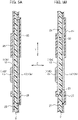
- a connecting portion (through hole) 23 may be provided as illustrated in FIG. 5B . That is, the front dummy land 13a and the rear dummy land 13b may be connected to each other by the connecting portion 23 penetrating the FPC 9.
- the connecting portion 23 is also made of a conductive material such as metal similarly as the lands.
- the solder 15 is also arranged on the dummy land 13, and the divided laser beam 19B is irradiated toward the dummy land 13, and the solder 15 is temporarily melted and fixed to the dummy land 13.
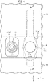
- the dummy land 13 may be covered with a cover lay 25 provided integrally with the FPC 9.
- the cover lay 25 is formed in a plate shape and has a thickness direction in the Z direction.
- the cover lay 25 covers both ends of the dummy land 13 in the longitudinal direction (Y direction). In other words, both ends of the dummy land 13 in the longitudinal direction are interposed between the FPC 9 and the cover lay 25.
- the plurality of lands are composed of odd number of terminal installation lands 11 and one dummy land 13.
- each of the two split laser beams 19A, 19B is irradiated toward each of the two lands 11 (11, 13).
- the two lands 11 (11, 13) are composed of two terminal installation lands 11, or one terminal installation land 11 and one dummy land 13.
- the terminal 3 when the terminal 3 is fixed to each of the plurality of lands 11 of the FPC 9 by repeating laser welding using the two split laser beams 19A, 19B a plurality of times, productivity can be improved.
- the occurrence of a failure in the FPC 9 by the laser beam 19 can be prevented. That is, since the total number of the terminal installation lands 11 and the dummy lands 13 is an even number, the two split laser beams 19A, 19B are not irradiated to the part of the FPC 9 where the lands are not provided. Then, it is prevented that a failure such as burning of a part of the FPC 9 irradiated with the split laser beams 19A, 19B occurs.
- the dummy land 13 is larger than the terminal installation land 11. Thus, damage to the FPC 9 is prevented when the divided laser beam 19A is irradiated toward the terminal installation land 11 and the divided laser beam 19B is irradiated toward the dummy land 13.
- the dummy lands 13 illustrated in FIG. 1 are not provided. Therefore, when the split laser beam 19A is irradiated toward one terminal installation land 11, the split laser beam 19B is irradiated to a portion of the FPC 9 where the land is not provided.
- the dummy land 13 is provided on both sides in the thickness direction of the FPC 9, the adjustment range of the heat capacity of the dummy lands 13 can be widened, and the value of the heat capacity of the dummy lands 13 can be easily increased.
- the terminal fixing method since the area of the front dummy land 13a and the area of the rear dummy land 13b are different from each other, it is possible to widen the adjustment range of the heat capacity of the dummy land 13 by effectively utilizing the vacant portions of the front and rear surfaces of the FPC 9.
- the front dummy land 13a and the rear dummy land 13b may be connected to each other by the through hole 23.
- heat conduction between the front dummy land 13a and the rear dummy land 13b is made smoother, and the size of the dummy land 13 can be reduced.
- solder solder for the dummy land
- the solder for the dummy land 13 also contributes to increasing the value of the heat capacity, and the size of the dummy land 13 can be reduced.
- the terminal fixing method since the terminal is not installed on the dummy land 13, there is a possibility that the dummy land 13 is peeled off from the FPC 9 due to the impact of the solder weight.
- the cover lay 25 provided integrally with the FPC 9
- the dummy land 13 is suppressed by the cover lay 25.
- peeling of the dummy land 13 from the FPC 9 can be prevented.
- the substrate 9 can be prevented from being damaged by the laser beam 19. More specifically, when the substrate 9 is a rigid substrate, the thickness thereof is about 0.3 mm to 1.6 mm. Therefore, even if the dummy land 13 is not provided, the rigid substrate itself is hardly damaged by the irradiation of the laser beam 19, such as by burning.
- FPC flexible printed circuit
- the thickness is about 12 ⁇ m to 50 ⁇ m. Therefore, if the dummy land 13 is not provided, the FPC 9 itself is highly likely to suffer damage such as burning due to irradiation of the laser beam 19. However, since the dummy land 13 and the like are provided, the heat of the irradiation of the laser beam 19 can be absorbed, and the occurrence of damage such as burning can be avoided.
- the FPC 9 When irradiating the laser beam 19 toward the terminal installation land 11 and the dummy land 13, positioning of the FPC 9 with respect to the laser irradiator 21 is naturally required. Therefore, as illustrated in FIG. 1 , the FPC 9 is positioned with respect to the connector 5 by positioning pins 31. The laser irradiator 21 is appropriately moved and positioned with respect to the connector 5 which is hardly elastic and can be regarded as almost rigid, and the irradiation of the laser beam 19 is directed to the terminal installation land 11 and the dummy land 13. Although the FPC 9 is flexible, it hardly deforms in the X direction and the Y direction illustrated in FIG. 1 , and can be regarded as a substantially rigid body for the forces in the X direction and the Y direction.
- the embodiment has been described above, the embodiment is not limited thereto, and various modifications can be made within the scope of the gist of the embodiment.
- the laser beam is divided into two, but the laser beam may be divided into N pieces, where "N" is any natural number equal to or greater than 3.
- the number of lands of the land group 10A is a multiple of "N".
Landscapes
- Engineering & Computer Science (AREA)
- Physics & Mathematics (AREA)
- Optics & Photonics (AREA)
- Manufacturing & Machinery (AREA)
- Mechanical Engineering (AREA)
- Plasma & Fusion (AREA)
- Microelectronics & Electronic Packaging (AREA)
- Electric Connection Of Electric Components To Printed Circuits (AREA)
- Manufacturing Of Electrical Connectors (AREA)
- Printing Elements For Providing Electric Connections Between Printed Circuits (AREA)
- Combinations Of Printed Boards (AREA)
Abstract
Description
- The present invention relates to a terminal fixing method.
- In order to detect voltage of a battery, it is necessary to join a voltage detection wiring member (FPC: Flexible Printed Circuits) to a connector. Therefore, there is known a terminal-connected FPC in which lands are set in the FPC and connector terminals are projected from the lands.
- In the terminal-connected FPC, the FPC is joined to the connector by using the connector terminals. In the terminal-connected FPC, the connector terminals (connector terminal pins) are joined to the lands of the FPC by laser soldering (laser welding). That is, the solder is temporarily melted by the laser beam, and then the solder is solidified to fix the connector terminals to the lands of the FPC.
- Here, in order to improve the productivity of the terminal-connected FPC, the laser irradiation method by the laser soldering may be changed from the single method to the prism method.
- That is, the two connector terminals are fixed to the lands of the FPC by simultaneously irradiating the two laser beams emitted from one laser oscillator and divided into two by the prism toward the two lands. Patent Document 1 (
JP 2009 - 019975 A - By the way, in the case where the prism method is employed, if the pin arrangement of the connector terminals is an odd number, a situation occurs in which a laser beam is irradiated to a portion where a connector terminal is not present. As a result, the FPC is burned down and the appearance of the insulation (such as measling) is defective.
- That is, when the number of lands adjacent to each other is an odd number, two laser beams are applied to each of the plurality of lands and the connector terminal, so that the last land and one connector terminal fixed to the land remain.
- When one laser beam out of the two laser beams is irradiated toward the remaining one land, the other laser beam out of the two laser beams is irradiated to the FPC, and the part of the FPC irradiated with the other laser beam is burnt. This problem also occurs when the terminals are installed on a substrate other than the FPC.
- An object or the present invention is to provide a terminal fixing method for fixing a terminal to each of a plurality of lands of a substrate by laser welding, which prevents a defect from being generated in the substrate by a laser beam while improving productivity.
- A terminal fixing method according to the invention is a terminal fixing method for fixing one ore more terminals to a plurality of lands provided on a substrate by laser welding, and includes: constructing the plurality of lands by one or more terminal installation lands on which the terminals are installed and one or more dummy lands each larger than each of the terminal installation lands; and irradiating each of divided laser beams emitted from a laser oscillator toward a corresponding land of two or more lands in the plurality of lands so as executing the laser welding, wherein the two or more lands are constructed by two or more terminal installation lands in the terminal installation lands, or one or more terminal installation lands in the terminal installation lands and the one or more dummy lands.
- According to the present invention, there is provided a terminal fixing method for fixing a terminal to each of a plurality of lands of a substrate by laser welding, which has the effect of preventing the substrate from being damaged by laser light while improving productivity.
-
-
FIG. 1 is a plan view (viewed in the Z direction) illustrating a state in which a terminal-connected FPC manufactured using a terminal fixing method according to an embodiment is installed in a connector. -
FIG. 2A is an enlarged view of a portion of IIA inFIG. 1 . -
FIG. 2B illustrates a cross-sectional view of IIB-IIB inFIG. 2A . -
FIG. 3A is a plan view of a dummy land as viewed from a front side. -
Figure 3B is a plan view of the dummy land as viewed from a rear side. -
FIG. 4 is a plan view of a terminal installation land and the dummy land provided with a cover lay. -
FIG. 5A illustrates a cross-sectional view of VA-VA inFIG. 4 . -
FIG. 5B is a view illustrating a structure in which a through hole is provided inFIG. 5A . - A terminal-connected substrate (e.g., a terminal-connected FPC) 1 according to an embodiment is used, for example, for detecting voltage of a battery mounted on a vehicle. As illustrated in
FIG. 1 , the terminal-connected FPC 1 is connected to aconnector 5 by using terminals (connector terminals) 3 provided on the terminal-connectedFPC 1. Theconnector 5 is connected to an ECU (Electronic Control Unit) 7. - The terminal-connected
substrate 1 includes a substrate (e.g., FPC) 9, a plurality of lands, and a plurality ofterminals 3. The plurality of lands are constituted ofterminal installation lands 11 anddummy lands 13. The FPC 9 includes a plate-like substrate body portion made of an insulating synthetic resin or the like, and a circuit portion (not illustrated) provided on the substrate body portion. Hereinafter, when "FPC" is referred to, the "FPC" refers to the substrate body portion excluding the circuit portion. - Here, for convenience of explanation, a predetermined direction in space is referred to as a X direction, a predetermined direction orthogonal to the X direction is referred to as a Y direction, and a direction orthogonal to the X direction and the Y direction is referred to as a Z direction.
- The terminal installation lands 11, the
dummy lands 13, and theterminals 3 are made of conductive materials such as metals. Theterminal installation lands 11 are appropriately connected to the circuit portion (not illustrated). Thedummy lands 13 are separated from the circuit portion (not illustrated). - Each of the
terminal installation lands 11 and thedummy lands 13 is formed in a thin film shape and is provided on the surface of the FPC 9 so that the thickness direction coincides with the thickness direction of the FPC 9. The thickness direction of theFPC 9, the thickness direction of theterminal installation lands 11, and the thickness direction of thedummy lands 13 are in the Z direction. - Each of the
terminal installation lands 11 is formed, for example, in a rectangular shape when viewed in the Z direction. An odd number of the plurality ofterminal installation lands 11 are provided on the FPC 9 so as to be adjacent to each other in the X direction with a fixed interval therebetween. The shapes of theterminal installation lands 11 are identical to each other. - Each of the
dummy lands 13 is formed in, for example, a rectangular shape or a deformed rectangular shape when viewed in the Z direction, formed larger than theterminal installation lands 11, and provided with an odd number (e.g., one). Onedummy land 13 is provided in the FPC 9 adjacent to theterminal installation land 11. - More specifically, the plurality of
terminal installation lands 11 and the onedummy land 13 are provided on the FPC 9 so as to be spaced apart from each other and adjacent to each other in the X direction. The pitch of the plurality ofterminal installation lands 11 and the onedummy land 13 in the X direction is constant. Further, the onedummy land 13 is adjacent to, for example, aterminal installation land 11 located at the most end of the plurality ofterminal installation lands 11. The total number of the plurality ofterminal installation lands 11 and the number of the onedummy land 13 is an even number. - Each of the
terminals 3 is fixed to each of the plurality ofterminal installation lands 11 by solder (e.g., soft solder) 15. Thedummy land 13 is not provided with a terminal. - The lands consisting of the
terminal installation lands 11 and thedummy lands 13 are provided as a plurality of groups, for example, as illustrated inFIG. 1 . That is, aland group 10A of a group A consisting of eight lands, and aland group 10B of a group B, a land group 10C of a group C, aland group 10D of a group D, and aland group 10E of a group E each consisting of a plurality of even numbered lands constitute a plurality of groups. In any of theland groups 10A to 10E, a plurality ofterminal installation lands 11 or oneterminal installation land 11, and onedummy land 13 are arranged at a fixed interval in the X direction. - Here, a mode of fixing the terminal 3 (a mode of installation on the FPC 9) will be described in detail.
- As illustrated in
FIGS. 2A and 2B , each of theterminals 3 is formed in a columnar shape such as a cylindrical shape. The terminal installation lands 11 are provided, for example, on a front surface and a rear surface of theFPC 9. Theterminal installation land 11 provided on the front surface of theFPC 9 and theterminal installation land 11 provided on the rear surface of theFPC 9 are formed in the same shape, for example. When viewed in the Z direction, all of the terminal installation lands 11 provided on the front surface of theFPC 9 and all of the terminal installation lands 11 provided on the rear surface of theFPC 9 overlap each other. - The terminal installation lands 11 provided on the front surface of the
FPC 9 and the terminal installation lands 11 provided on the rear surface of theFPC 9 may be formed in different shapes and sizes. When viewed in the Z direction, a part of theterminal installation land 11 provided on the front surface of theFPC 9 and a part of theterminal installation land 11 provided on the rear surface of theFPC 9 may overlap each other. Further, when viewed in the Z direction, all of the terminal installation lands 11 provided on the rear surface of theFPC 9 may be housed inside the terminal installation lands 11 provided on the front surface of theFPC 9, or all of the terminal installation lands 11 provided on the front surface of theFPC 9 may be housed inside the terminal installation lands 11 provided on the rear surface of theFPC 9. - The
FPC 9 and the terminal installation lands 11 are provided with, for example, throughholes 17 each formed in a cylindrical shape. The inner diameter of the throughhole 17 is slightly larger than the outer diameter of theterminal 3. The central axis of the throughhole 17 and the central axis of theterminal installation land 11 extend in the Z direction and are substantially coincident with each other. The terminal 3 passes through the throughhole 17. - The front side part of the
solder 15 is provided for fixing theterminal 3 to theterminal installation land 11 of theFPC 9. The front side portion of thesolder 15 is in contact with the surface of theterminal installation land 11 provided on the front surface of theFPC 9 and the portion of theterminal 3 projecting from the surface of theterminal installation land 11. - The rear side portion of the
solder 15 is in contact with the surface of theterminal installation land 11 provided on the rear surface of theFPC 9 and the portion of theterminal 3 protruding from the surface of theterminal installation land 11. - Further, the
solder 15 enters a gap between the terminal 3 and the throughhole 17. The front side portion of thesolder 15 and the rear side portion of thesolder 15 are connected to each other by such an entered part of thesolder 15. - The dummy lands 13 are also provided, for example, on the front surface and the rear surface of the
FPC 9. For example, the dummy lands 13 provided on the front surface of theFPC 9 and the dummy lands 13 provided on the rear surface of theFPC 9 are formed in the same shape. When viewed in the Z direction, all of the dummy lands 13 provided on the front surface of theFPC 9 and all of the dummy lands 13 provided on the rear surface of theFPC 9 overlap each other. - As illustrated in
FIGS. 3A and 3B , the dummy lands 13 provided on the front surface of theFPC 9 and the dummy lands 13 provided on the rear surface of theFPC 9 may be formed in different shapes and sizes. When viewed in the Z direction, a part of thedummy land 13 provided on the front surface of theFPC 9 and a part of thedummy land 13 provided on the rear surface of theFPC 9 may overlap each other. Further, when viewed in the Z direction, all of the dummy lands 13 provided on the front surface of theFPC 9 may be housed inside the dummy lands 13 provided on the rear surface of theFPC 9, or all of the dummy lands 13 provided on the rear surface of theFPC 9 may be housed inside the dummy lands 13 provided on the front surface of theFPC 9. - In addition, as illustrated in
FIGS. 2A and 2B ,solder 15 is also provided on the surface of thedummy land 13 provided on the front surface of theFPC 9. - Here, the fact that the
dummy land 13 is larger than theterminal installation land 11 will be described in more detail. - The
dummy land 13 is larger than theterminal installation land 11, for example, because the heat capacity of onedummy land 13 is larger than the heat capacity of oneterminal installation land 11. When the specific heat of thedummy land 13 and theterminal installation land 11 is equal to each other, the volume of onedummy land 13 is larger than the volume of oneterminal installation land 11. - The fact that the specific heat of the
dummy land 13 and theterminal installation land 11 is equal to each other will be described in more specifically. It is assumed that the value of the thickness dimension of theterminal installation land 11 is equal to the value of the thickness dimension of thedummy land 13. When viewed in the Z direction, the area of onedummy land 13 is larger than the area of oneterminal installation land 11. - Further, the area of the dummy land 13 (13a) provided on the front surface of the
FPC 9 is larger than the area of theterminal installation land 11 provided on the front surface of theFPC 9. The area of the dummy land 13 (13b) provided on the rear surface of theFPC 9 is larger than the area of theterminal installation land 11 provided on the rear surface of theFPC 9. - If the heat capacity of the
dummy land 13 is larger than the heat capacity of theterminal installation land 11, it is not necessary to maintain the above-mentioned relationship with respect to the area of theterminal installation land 11 on the front and rear surfaces of theFPC 9 and the area of thedummy land 13 on the front and rear surfaces of theFPC 9. However, when the value of the thermal conductivity of theFPC 9 is smaller than the values of the thermal conductivity of theterminal installation land 11 and thedummy land 13, the area of theterminal installation land 11 and the area of thedummy land 13 on the front and rear surfaces of theFPC 9 should be determined in consideration of the relationship of the thermal conductivity. - The
terminal installation land 11 is provided with the solder 15 (15A) and theterminal 3, and thedummy land 13 is provided with the solder 15 (15B). The heat capacity of theterminal installation land 11 and the heat capacity of thedummy land 13 can be determined in consideration of the installation of thesolder 15 and theterminal 3. - That is, the sum of the heat capacity of the
terminal installation land 11, the heat capacity of thesolder 15A, and the heat capacity of theterminal 3 may be made approximately equal to the sum of the heat capacity of thedummy land 13 and the heat capacity of thesolder 15B. The heat capacity of thesolder 15 includes the heat of fusion of thesolder 15. - Next, a terminal fixing method will be described. The terminal fixing method may be a method of installing the terminal, a method of connecting the terminal, or a method of fixing the terminal to the substrate. A case where the
terminals 3 are fixed to theland group 10A of the group A illustrated inFIG. 1 will be described as an example. When theterminals 3 are fixed to theland group 10B of the group B or the like, the same operation is performed as when theterminals 3 are fixed to theland group 10A of the group A. - The terminal fixing method is a method in which a plurality of
terminals 3 are fixed to the land group (lands of the first group) 10A of the group A provided in theFPC 9 to be integrally provided by laser welding. - As described above, the
land group 10A of the first group (group A) consists of an odd number of a plurality of terminal installation lands 11 on which theterminals 3 are installed, and an odd number of dummy lands (e.g., one dummy land) 13. - Further, since one
terminal 3 is installed on oneterminal installation land 11, no terminal is installed on thedummy land 13. - Laser welding is performed by using a
laser irradiator 21 for executing a prism method. In laser welding, a split laser beam 19 (19A, 19B) emitted from one laser oscillator of thelaser irradiator 21 and divided into a plurality of parts (e.g., two parts) by a prism is used. Thesplit laser beams laser irradiator 21, the intensities of thesplit laser beams split laser beams - In laser welding, each of the
split laser beams land group 10A of the first group. - In the irradiation with the
split laser beams split laser beams - In a state before the laser welding, the
terminal 3 is appropriately inserted into the through-hole 17 provided at theterminal installation land 11. In the state before laser welding, solder (e.g., thread solder) before melting is supplied to theterminal installation land 11 and theterminal 3 by a solder supply device (not illustrated). In the state before laser welding, solder before melting (e.g., thread solder) is similarly supplied to thedummy land 13. - The supplied
solder 15 is temporarily melted by irradiation ofsplit laser beams FIG. 2B , theterminal 3 is fixed to theterminal installation land 11 by thesolder 15A, and thesolder 15B is installed on thedummy land 13. - Since only the
solder 15 is melted by thesplit laser beams solder 15 is melted. - The laser welding is repeated a plurality of times while appropriately moving and positioning the
laser irradiator 21 with respect to theFPC 9 or the like, so that dividedlaser beams lands - It will be explained further with an example. As illustrated in
FIGS. 2A and 2B , thesplit laser beams FIG. 1 , theland group 10A is provided with seven terminal installation lands 11 and onedummy land 13. - In the first laser welding, each of the two
split laser beams first land 11A for terminal installation and thesecond land 11B for terminal installation adjacent to each other. - In the second laser welding, each of the two
split laser beams terminal installation land 11C and the fourthterminal installation land 11D adjacent to each other. - In the third laser welding, each of the two
split laser beams terminal installation land 11E and the sixthterminal installation land 11F adjacent to each other. - In the fourth laser welding, each of the two
split laser beams terminal installation land 11G and onedummy land 13 adjacent to each other. - The third laser welding is performed by the
laser irradiator 21 at the position indicated by reference numeral P1 inFIG. 2B . The fourth laser welding is performed by thelaser irradiator 21 at the position indicated by reference numeral P2 inFIG. 2B . - As described above, the
dummy land 13 consists of a frontsurface dummy land 13a provided on the front surface as one surface of the thickness direction of theFPC 9 and a rearsurface dummy land 13b provided on the rear surface as other surface of the thickness direction of theFPC 9. - The area of the
front dummy land 13a and the area of therear dummy land 13b are different from each other. For example, as illustrated inFIGS. 3A and 3B , the area of therear dummy land 13b is larger than the area of thefront dummy land 13a. - Each of the shape of the
front dummy land 13a and the shape of therear dummy land 13b illustrated inFIGS. 3A and 3B includes a wide portion (a portion having a large value in the X direction) and a narrow portion (a portion having a small value in the X direction), and is elongated in the Y direction. This is because the circuit portion (not illustrated) of theFPC 9 is avoided. Thedummy land 13 may have a shape other than those illustrated inFIGS. 3A and 3B . - Further, although the
front dummy land 13a and therear dummy land 13b are disconnected by theFPC 9 between them as illustrated inFIG. 5A , a connecting portion (through hole) 23 may be provided as illustrated inFIG. 5B . That is, thefront dummy land 13a and therear dummy land 13b may be connected to each other by the connectingportion 23 penetrating theFPC 9. The connectingportion 23 is also made of a conductive material such as metal similarly as the lands. - In the laser welding, as described above, the
solder 15 is also arranged on thedummy land 13, and the dividedlaser beam 19B is irradiated toward thedummy land 13, and thesolder 15 is temporarily melted and fixed to thedummy land 13. - As illustrated in
FIGS. 4 ,5A, and 5B , in the terminal-connectedFPC 1, at least a part of thedummy land 13 may be covered with a cover lay 25 provided integrally with theFPC 9. The cover lay 25 is formed in a plate shape and has a thickness direction in the Z direction. The cover lay 25 covers both ends of thedummy land 13 in the longitudinal direction (Y direction). In other words, both ends of thedummy land 13 in the longitudinal direction are interposed between theFPC 9 and the cover lay 25. - In the terminal fixing method according to the embodiment, the plurality of lands are composed of odd number of terminal installation lands 11 and one
dummy land 13. In the laser welding, each of the twosplit laser beams terminal installation land 11 and onedummy land 13. - Thus, when the
terminal 3 is fixed to each of the plurality oflands 11 of theFPC 9 by repeating laser welding using the twosplit laser beams split laser beams FPC 9 by thelaser beam 19 can be prevented. That is, since the total number of the terminal installation lands 11 and the dummy lands 13 is an even number, the twosplit laser beams FPC 9 where the lands are not provided. Then, it is prevented that a failure such as burning of a part of theFPC 9 irradiated with thesplit laser beams - The
dummy land 13 is larger than theterminal installation land 11. Thus, damage to theFPC 9 is prevented when the dividedlaser beam 19A is irradiated toward theterminal installation land 11 and the dividedlaser beam 19B is irradiated toward thedummy land 13. - In a terminal fixing method according to a comparative example, for example, the dummy lands 13 illustrated in
FIG. 1 are not provided. Therefore, when thesplit laser beam 19A is irradiated toward oneterminal installation land 11, thesplit laser beam 19B is irradiated to a portion of theFPC 9 where the land is not provided. - Further, in the terminal fixing method according to the embodiment, since the
dummy land 13 is provided on both sides in the thickness direction of theFPC 9, the adjustment range of the heat capacity of the dummy lands 13 can be widened, and the value of the heat capacity of the dummy lands 13 can be easily increased. - Further, in the terminal fixing method according to the embodiment, since the area of the
front dummy land 13a and the area of therear dummy land 13b are different from each other, it is possible to widen the adjustment range of the heat capacity of thedummy land 13 by effectively utilizing the vacant portions of the front and rear surfaces of theFPC 9. - In the terminal fixing method according to the embodiment, the
front dummy land 13a and therear dummy land 13b may be connected to each other by the throughhole 23. Thus, heat conduction between thefront dummy land 13a and therear dummy land 13b is made smoother, and the size of thedummy land 13 can be reduced. - Further, in the terminal fixing method according to the embodiment, when the laser welding is performed, solder (solder for the dummy land) is arranged on the
dummy land 13, and the divided laser beam is irradiated toward thedummy land 13. Thus, the solder for thedummy land 13 also contributes to increasing the value of the heat capacity, and the size of thedummy land 13 can be reduced. - Further, in the terminal fixing method according to the embodiment, since the terminal is not installed on the
dummy land 13, there is a possibility that thedummy land 13 is peeled off from theFPC 9 due to the impact of the solder weight. However, by covering at least a part of thedummy land 13 with the cover lay 25 provided integrally with theFPC 9, thedummy land 13 is suppressed by the cover lay 25. Thus, peeling of thedummy land 13 from theFPC 9 can be prevented. - Further, even when the
substrate 9 is a flexible printed circuit (FPC) by the terminal fixing method according to the embodiment, thesubstrate 9 can be prevented from being damaged by thelaser beam 19. More specifically, when thesubstrate 9 is a rigid substrate, the thickness thereof is about 0.3 mm to 1.6 mm. Therefore, even if thedummy land 13 is not provided, the rigid substrate itself is hardly damaged by the irradiation of thelaser beam 19, such as by burning. - When the
substrate 9 is an FPC, the thickness is about 12 µm to 50 µm. Therefore, if thedummy land 13 is not provided, theFPC 9 itself is highly likely to suffer damage such as burning due to irradiation of thelaser beam 19. However, since thedummy land 13 and the like are provided, the heat of the irradiation of thelaser beam 19 can be absorbed, and the occurrence of damage such as burning can be avoided. - When irradiating the
laser beam 19 toward theterminal installation land 11 and thedummy land 13, positioning of theFPC 9 with respect to thelaser irradiator 21 is naturally required. Therefore, as illustrated inFIG. 1 , theFPC 9 is positioned with respect to theconnector 5 by positioning pins 31. Thelaser irradiator 21 is appropriately moved and positioned with respect to theconnector 5 which is hardly elastic and can be regarded as almost rigid, and the irradiation of thelaser beam 19 is directed to theterminal installation land 11 and thedummy land 13. Although theFPC 9 is flexible, it hardly deforms in the X direction and the Y direction illustrated inFIG. 1 , and can be regarded as a substantially rigid body for the forces in the X direction and the Y direction. - Although the embodiment has been described above, the embodiment is not limited thereto, and various modifications can be made within the scope of the gist of the embodiment. For example, in the above description, the laser beam is divided into two, but the laser beam may be divided into N pieces, where "N" is any natural number equal to or greater than 3. In this case, for example, the number of lands of the
land group 10A is a multiple of "N".
Claims (7)
- A terminal fixing method for fixing one ore more terminals (3) to a plurality of lands (11, 13) provided on a substrate (9) by laser welding, comprising:constructing the plurality of lands (11, 13) by one ore more terminal installation lands (11) on which the terminals (3) are installed and one or more dummy lands (13) each larger than each of the terminal installation lands (11); andirradiating each of divided laser beams (19; 19A, 19B) emitted from a laser oscillator (21) toward a corresponding land of two or more lands in the plurality of lands (11, 13) so as executing the laser welding, whereinthe two or more lands are constructed by two or more terminal installation lands in the terminal installation lands (11), or one or more terminal installation lands in the terminal installation lands (11) and the one or more dummy lands (13).
- The terminal fixing method of claim 1, wherein
each of the dummy lands (13) comprises a front surface dummy land (13a) provided on one surface in a thickness direction of the substrate (9) and a rear surface dummy land (13b) provided on other surface in the thickness direction of the substrate (9). - The terminal fixing method of claim 2, wherein
an area of the front surface dummy land (13a) and an area of the rear surface dummy land (13b) are different from each other. - The terminal fixing method of claim 2 or 3, wherein
the front surface dummy land (13a) and the rear surface dummy land (13b) are mutually connected by a connection part (23) penetrating the substrate (9). - The terminal fixing method of any one of claims 1 to 4, wherein
in the laser welding, a solder (15B) is arranged on each of the one or more dummy lands (13), and the laser beams (19B) are irradiated toward the one or more dummy lands (13). - The terminal fixing method of any one of claims 1 to 5, wherein
at least a part of a dummy land in the one or more dummy lands (13) is covered with a cover lay (25) provided on the substrate (9). - The terminal fixing method of any one of claims 1 to 6, wherein
the substrate (9) is a flexible printed circuit.
Applications Claiming Priority (1)
| Application Number | Priority Date | Filing Date | Title |
|---|---|---|---|
| JP2020201601A JP7315523B2 (en) | 2020-12-04 | 2020-12-04 | Terminal fixing method |
Publications (2)
| Publication Number | Publication Date |
|---|---|
| EP4008469A1 true EP4008469A1 (en) | 2022-06-08 |
| EP4008469B1 EP4008469B1 (en) | 2023-01-18 |
Family
ID=78820298
Family Applications (1)
| Application Number | Title | Priority Date | Filing Date |
|---|---|---|---|
| EP21211663.6A Active EP4008469B1 (en) | 2020-12-04 | 2021-12-01 | Terminal fixing method |
Country Status (4)
| Country | Link |
|---|---|
| US (1) | US12592533B2 (en) |
| EP (1) | EP4008469B1 (en) |
| JP (1) | JP7315523B2 (en) |
| CN (1) | CN114597727B (en) |
Cited By (1)
| Publication number | Priority date | Publication date | Assignee | Title |
|---|---|---|---|---|
| US20240408701A1 (en) * | 2022-07-26 | 2024-12-12 | BOE MLED Technology Co., Ltd. | Welding-pad repair device and pad repair method |
Families Citing this family (1)
| Publication number | Priority date | Publication date | Assignee | Title |
|---|---|---|---|---|
| JP2025030373A (en) | 2023-08-23 | 2025-03-07 | 矢崎総業株式会社 | Circuit body and circuit body with connector |
Citations (5)
| Publication number | Priority date | Publication date | Assignee | Title |
|---|---|---|---|---|
| US6333483B1 (en) * | 1997-04-04 | 2001-12-25 | Taiyo Yuden Co., Ltd. | Method of manufacturing circuit modules |
| US20070097309A1 (en) * | 2005-10-31 | 2007-05-03 | Tomohiro Matsumoto | Display device |
| US20090015276A1 (en) * | 2007-07-11 | 2009-01-15 | Kabushiki Kaisha Nihon Micronics | Probe assembly and method for producing it |
| US7677905B2 (en) * | 2006-12-13 | 2010-03-16 | Denso Corporation | Electronic device and manufacturing method of the same |
| JP2016085163A (en) * | 2014-10-28 | 2016-05-19 | 京セラ株式会社 | Circuit board and circuit device |
Family Cites Families (17)
| Publication number | Priority date | Publication date | Assignee | Title |
|---|---|---|---|---|
| US3586813A (en) * | 1967-08-31 | 1971-06-22 | Western Electric Co | Simultaneous multiple lead bonding |
| JPS62104194A (en) * | 1985-10-31 | 1987-05-14 | キヤノン株式会社 | Double-sided printed wiring board for laser soldering |
| DE3831743A1 (en) | 1988-09-17 | 1990-03-29 | Philips Patentverwaltung | DEVICE FOR MACHINING A WORKPIECE WITH LASER LIGHT AND USE OF THIS DEVICE |
| JPH0521515A (en) * | 1991-07-15 | 1993-01-29 | Seiko Epson Corp | Liquid crystal display device and manufacturing method thereof |
| US5495089A (en) * | 1993-06-04 | 1996-02-27 | Digital Equipment Corporation | Laser soldering surface mount components of a printed circuit board |
| JP3395621B2 (en) * | 1997-02-03 | 2003-04-14 | イビデン株式会社 | Printed wiring board and manufacturing method thereof |
| JPH10335806A (en) * | 1997-04-04 | 1998-12-18 | Taiyo Yuden Co Ltd | Method and apparatus for manufacturing circuit module |
| JP2003069163A (en) * | 2001-08-22 | 2003-03-07 | Olympus Optical Co Ltd | Flexible printed circuit board |
| JP2005050603A (en) | 2003-07-31 | 2005-02-24 | Yazaki Corp | Terminal fixing method |
| JP2007265962A (en) | 2006-02-28 | 2007-10-11 | Hitachi Ltd | Laser welding method, control unit manufacturing method, and vehicle control unit |
| KR100912037B1 (en) * | 2007-12-03 | 2009-08-12 | (주)엘지하우시스 | Method for manufacturing a solar cell module and an equipment therefor |
| JP4433058B2 (en) * | 2008-01-30 | 2010-03-17 | 株式会社デンソー | Electronic device and manufacturing method thereof |
| JP5535408B1 (en) | 2012-07-09 | 2014-07-02 | 古河電気工業株式会社 | Crimp terminal, connection structure and connector |
| JP6329027B2 (en) * | 2014-08-04 | 2018-05-23 | ミネベアミツミ株式会社 | Flexible printed circuit board |
| JP6390354B2 (en) | 2014-11-06 | 2018-09-19 | オムロン株式会社 | Terminal fixing device and terminal fixing method |
| JP2017010984A (en) * | 2015-06-17 | 2017-01-12 | 日本電産サンキョー株式会社 | Circuit board |
| JP2025104194A (en) | 2023-12-27 | 2025-07-09 | 株式会社ユピテル | Systems and programs |
-
2020
- 2020-12-04 JP JP2020201601A patent/JP7315523B2/en active Active
-
2021
- 2021-12-01 EP EP21211663.6A patent/EP4008469B1/en active Active
- 2021-12-02 CN CN202111460088.1A patent/CN114597727B/en active Active
- 2021-12-02 US US17/541,005 patent/US12592533B2/en active Active
Patent Citations (6)
| Publication number | Priority date | Publication date | Assignee | Title |
|---|---|---|---|---|
| US6333483B1 (en) * | 1997-04-04 | 2001-12-25 | Taiyo Yuden Co., Ltd. | Method of manufacturing circuit modules |
| US20070097309A1 (en) * | 2005-10-31 | 2007-05-03 | Tomohiro Matsumoto | Display device |
| US7677905B2 (en) * | 2006-12-13 | 2010-03-16 | Denso Corporation | Electronic device and manufacturing method of the same |
| US20090015276A1 (en) * | 2007-07-11 | 2009-01-15 | Kabushiki Kaisha Nihon Micronics | Probe assembly and method for producing it |
| JP2009019975A (en) | 2007-07-11 | 2009-01-29 | Micronics Japan Co Ltd | Probe assembly and manufacturing method thereof |
| JP2016085163A (en) * | 2014-10-28 | 2016-05-19 | 京セラ株式会社 | Circuit board and circuit device |
Cited By (2)
| Publication number | Priority date | Publication date | Assignee | Title |
|---|---|---|---|---|
| US20240408701A1 (en) * | 2022-07-26 | 2024-12-12 | BOE MLED Technology Co., Ltd. | Welding-pad repair device and pad repair method |
| US12491580B2 (en) * | 2022-07-26 | 2025-12-09 | BOE MLED Technology Co., Ltd. | Welding-pad repair device and pad repair method |
Also Published As
| Publication number | Publication date |
|---|---|
| US12592533B2 (en) | 2026-03-31 |
| JP2022089301A (en) | 2022-06-16 |
| CN114597727B (en) | 2023-08-15 |
| US20220181832A1 (en) | 2022-06-09 |
| JP7315523B2 (en) | 2023-07-26 |
| EP4008469B1 (en) | 2023-01-18 |
| CN114597727A (en) | 2022-06-07 |
Similar Documents
| Publication | Publication Date | Title |
|---|---|---|
| JP6966046B2 (en) | FPCB assembly for battery module, its manufacturing method and battery module including it | |
| EP4008469B1 (en) | Terminal fixing method | |
| US6295210B1 (en) | Chassis grounding ring for a printed wiring board mounting aperture | |
| US12176640B2 (en) | Forming connections to flexible interconnect circuits | |
| US9780468B2 (en) | Connector comprising shell and two additional members | |
| EP1753281A2 (en) | Double ended guide pin assembly | |
| US20200020919A1 (en) | Circuit body and battery module | |
| WO2020071069A1 (en) | Flexible printed circuit board, and wiring module | |
| US10833373B2 (en) | Battery module | |
| US6955551B2 (en) | Card edge connector jig and card edge connector connection mechanism | |
| GB2422491A (en) | Printed circuit board | |
| DE3536963A1 (en) | ASSEMBLY ARRANGEMENT | |
| JP2004304172A (en) | Method and structure for reinforcing interconnection performance between land-grid-array (lga) module, and printed wiring board | |
| US20190006777A1 (en) | Printed Circuit Board Solder Joints | |
| US7311241B2 (en) | Method of mounting terminal on printed board, terminal mounted printed board and electric connection box accommodating the terminal mounted printed board, which are formed by the method | |
| US20070107935A1 (en) | Method and apparatus for electrically connecting printed circuit boards or other panels | |
| JP2008091610A (en) | Printed-circuit board | |
| WO2021075165A1 (en) | Wiring module | |
| US6657137B2 (en) | Connection structure and connection method of for connecting two circuit boards | |
| CN116357916B (en) | Vehicle headlamp module | |
| US10225926B2 (en) | Contact arrangement for a multi-layer circuit board | |
| JP2017157669A (en) | Electronic device and manufacturing method thereof | |
| JP2024037253A (en) | Connectors and electronic boards | |
| CN219959471U (en) | Switching FPC, display module assembly, display device and electronic equipment | |
| WO2022071015A1 (en) | Printed circuit board assembly and method for manufacturing printed circuit board assembly |
Legal Events
| Date | Code | Title | Description |
|---|---|---|---|
| PUAI | Public reference made under article 153(3) epc to a published international application that has entered the european phase |
Free format text: ORIGINAL CODE: 0009012 |
|
| STAA | Information on the status of an ep patent application or granted ep patent |
Free format text: STATUS: REQUEST FOR EXAMINATION WAS MADE |
|
| 17P | Request for examination filed |
Effective date: 20211201 |
|
| AK | Designated contracting states |
Kind code of ref document: A1 Designated state(s): AL AT BE BG CH CY CZ DE DK EE ES FI FR GB GR HR HU IE IS IT LI LT LU LV MC MK MT NL NO PL PT RO RS SE SI SK SM TR |
|
| RIC1 | Information provided on ipc code assigned before grant |
Ipc: H05K 1/11 20060101ALN20220728BHEP Ipc: H05K 1/03 20060101ALN20220728BHEP Ipc: H01R 12/58 20110101ALN20220728BHEP Ipc: B23K 26/067 20060101ALI20220728BHEP Ipc: B23K 1/00 20060101ALI20220728BHEP Ipc: H05K 3/34 20060101ALI20220728BHEP Ipc: H05K 3/32 20060101ALI20220728BHEP Ipc: H05K 3/30 20060101ALI20220728BHEP Ipc: H01R 43/02 20060101ALI20220728BHEP Ipc: G01R 1/073 20060101ALI20220728BHEP Ipc: B23K 1/005 20060101AFI20220728BHEP |
|
| RIC1 | Information provided on ipc code assigned before grant |
Ipc: H05K 1/11 20060101ALN20220801BHEP Ipc: H05K 1/03 20060101ALN20220801BHEP Ipc: H01R 12/58 20110101ALN20220801BHEP Ipc: B23K 26/067 20060101ALI20220801BHEP Ipc: B23K 1/00 20060101ALI20220801BHEP Ipc: H05K 3/34 20060101ALI20220801BHEP Ipc: H05K 3/32 20060101ALI20220801BHEP Ipc: H05K 3/30 20060101ALI20220801BHEP Ipc: H01R 43/02 20060101ALI20220801BHEP Ipc: G01R 1/073 20060101ALI20220801BHEP Ipc: B23K 1/005 20060101AFI20220801BHEP |
|
| RIC1 | Information provided on ipc code assigned before grant |
Ipc: H05K 1/11 20060101ALN20220809BHEP Ipc: H05K 1/03 20060101ALN20220809BHEP Ipc: H01R 12/58 20110101ALN20220809BHEP Ipc: B23K 26/067 20060101ALI20220809BHEP Ipc: B23K 1/00 20060101ALI20220809BHEP Ipc: H05K 3/34 20060101ALI20220809BHEP Ipc: H05K 3/32 20060101ALI20220809BHEP Ipc: H05K 3/30 20060101ALI20220809BHEP Ipc: H01R 43/02 20060101ALI20220809BHEP Ipc: G01R 1/073 20060101ALI20220809BHEP Ipc: B23K 1/005 20060101AFI20220809BHEP |
|
| GRAP | Despatch of communication of intention to grant a patent |
Free format text: ORIGINAL CODE: EPIDOSNIGR1 |
|
| STAA | Information on the status of an ep patent application or granted ep patent |
Free format text: STATUS: GRANT OF PATENT IS INTENDED |
|
| RIC1 | Information provided on ipc code assigned before grant |
Ipc: H05K 1/11 20060101ALN20220815BHEP Ipc: H05K 1/03 20060101ALN20220815BHEP Ipc: H01R 12/58 20110101ALN20220815BHEP Ipc: B23K 26/067 20060101ALI20220815BHEP Ipc: B23K 1/00 20060101ALI20220815BHEP Ipc: H05K 3/34 20060101ALI20220815BHEP Ipc: H05K 3/32 20060101ALI20220815BHEP Ipc: H05K 3/30 20060101ALI20220815BHEP Ipc: H01R 43/02 20060101ALI20220815BHEP Ipc: G01R 1/073 20060101ALI20220815BHEP Ipc: B23K 1/005 20060101AFI20220815BHEP |
|
| GRAS | Grant fee paid |
Free format text: ORIGINAL CODE: EPIDOSNIGR3 |
|
| INTG | Intention to grant announced |
Effective date: 20220920 |
|
| GRAA | (expected) grant |
Free format text: ORIGINAL CODE: 0009210 |
|
| STAA | Information on the status of an ep patent application or granted ep patent |
Free format text: STATUS: THE PATENT HAS BEEN GRANTED |
|
| RBV | Designated contracting states (corrected) |
Designated state(s): AL AT BE BG CH CY CZ DE DK EE ES FI FR GB GR HR HU IE IS IT LI LT LU LV MC MK MT NL NO PL PT RO RS SE SI SK SM TR |
|
| AK | Designated contracting states |
Kind code of ref document: B1 Designated state(s): AL AT BE BG CH CY CZ DE DK EE ES FI FR GB GR HR HU IE IS IT LI LT LU LV MC MK MT NL NO PL PT RO RS SE SI SK SM TR |
|
| REG | Reference to a national code |
Ref country code: GB Ref legal event code: FG4D |
|
| REG | Reference to a national code |
Ref country code: CH Ref legal event code: EP |
|
| REG | Reference to a national code |
Ref country code: DE Ref legal event code: R096 Ref document number: 602021001270 Country of ref document: DE |
|
| REG | Reference to a national code |
Ref country code: AT Ref legal event code: REF Ref document number: 1544403 Country of ref document: AT Kind code of ref document: T Effective date: 20230215 Ref country code: IE Ref legal event code: FG4D |
|
| REG | Reference to a national code |
Ref country code: LT Ref legal event code: MG9D |
|
| REG | Reference to a national code |
Ref country code: NL Ref legal event code: MP Effective date: 20230118 |
|
| RAP4 | Party data changed (patent owner data changed or rights of a patent transferred) |
Owner name: YAZAKI CORPORATION |
|
| REG | Reference to a national code |
Ref country code: AT Ref legal event code: MK05 Ref document number: 1544403 Country of ref document: AT Kind code of ref document: T Effective date: 20230118 |
|
| PG25 | Lapsed in a contracting state [announced via postgrant information from national office to epo] |
Ref country code: NL Free format text: LAPSE BECAUSE OF FAILURE TO SUBMIT A TRANSLATION OF THE DESCRIPTION OR TO PAY THE FEE WITHIN THE PRESCRIBED TIME-LIMIT Effective date: 20230118 |
|
| PG25 | Lapsed in a contracting state [announced via postgrant information from national office to epo] |
Ref country code: RS Free format text: LAPSE BECAUSE OF FAILURE TO SUBMIT A TRANSLATION OF THE DESCRIPTION OR TO PAY THE FEE WITHIN THE PRESCRIBED TIME-LIMIT Effective date: 20230118 Ref country code: PT Free format text: LAPSE BECAUSE OF FAILURE TO SUBMIT A TRANSLATION OF THE DESCRIPTION OR TO PAY THE FEE WITHIN THE PRESCRIBED TIME-LIMIT Effective date: 20230518 Ref country code: NO Free format text: LAPSE BECAUSE OF FAILURE TO SUBMIT A TRANSLATION OF THE DESCRIPTION OR TO PAY THE FEE WITHIN THE PRESCRIBED TIME-LIMIT Effective date: 20230418 Ref country code: LV Free format text: LAPSE BECAUSE OF FAILURE TO SUBMIT A TRANSLATION OF THE DESCRIPTION OR TO PAY THE FEE WITHIN THE PRESCRIBED TIME-LIMIT Effective date: 20230118 Ref country code: LT Free format text: LAPSE BECAUSE OF FAILURE TO SUBMIT A TRANSLATION OF THE DESCRIPTION OR TO PAY THE FEE WITHIN THE PRESCRIBED TIME-LIMIT Effective date: 20230118 Ref country code: HR Free format text: LAPSE BECAUSE OF FAILURE TO SUBMIT A TRANSLATION OF THE DESCRIPTION OR TO PAY THE FEE WITHIN THE PRESCRIBED TIME-LIMIT Effective date: 20230118 Ref country code: ES Free format text: LAPSE BECAUSE OF FAILURE TO SUBMIT A TRANSLATION OF THE DESCRIPTION OR TO PAY THE FEE WITHIN THE PRESCRIBED TIME-LIMIT Effective date: 20230118 Ref country code: AT Free format text: LAPSE BECAUSE OF FAILURE TO SUBMIT A TRANSLATION OF THE DESCRIPTION OR TO PAY THE FEE WITHIN THE PRESCRIBED TIME-LIMIT Effective date: 20230118 |
|
| PG25 | Lapsed in a contracting state [announced via postgrant information from national office to epo] |
Ref country code: SE Free format text: LAPSE BECAUSE OF FAILURE TO SUBMIT A TRANSLATION OF THE DESCRIPTION OR TO PAY THE FEE WITHIN THE PRESCRIBED TIME-LIMIT Effective date: 20230118 Ref country code: PL Free format text: LAPSE BECAUSE OF FAILURE TO SUBMIT A TRANSLATION OF THE DESCRIPTION OR TO PAY THE FEE WITHIN THE PRESCRIBED TIME-LIMIT Effective date: 20230118 Ref country code: IS Free format text: LAPSE BECAUSE OF FAILURE TO SUBMIT A TRANSLATION OF THE DESCRIPTION OR TO PAY THE FEE WITHIN THE PRESCRIBED TIME-LIMIT Effective date: 20230518 Ref country code: GR Free format text: LAPSE BECAUSE OF FAILURE TO SUBMIT A TRANSLATION OF THE DESCRIPTION OR TO PAY THE FEE WITHIN THE PRESCRIBED TIME-LIMIT Effective date: 20230419 Ref country code: FI Free format text: LAPSE BECAUSE OF FAILURE TO SUBMIT A TRANSLATION OF THE DESCRIPTION OR TO PAY THE FEE WITHIN THE PRESCRIBED TIME-LIMIT Effective date: 20230118 |
|
| REG | Reference to a national code |
Ref country code: DE Ref legal event code: R097 Ref document number: 602021001270 Country of ref document: DE |
|
| PG25 | Lapsed in a contracting state [announced via postgrant information from national office to epo] |
Ref country code: SM Free format text: LAPSE BECAUSE OF FAILURE TO SUBMIT A TRANSLATION OF THE DESCRIPTION OR TO PAY THE FEE WITHIN THE PRESCRIBED TIME-LIMIT Effective date: 20230118 Ref country code: RO Free format text: LAPSE BECAUSE OF FAILURE TO SUBMIT A TRANSLATION OF THE DESCRIPTION OR TO PAY THE FEE WITHIN THE PRESCRIBED TIME-LIMIT Effective date: 20230118 Ref country code: EE Free format text: LAPSE BECAUSE OF FAILURE TO SUBMIT A TRANSLATION OF THE DESCRIPTION OR TO PAY THE FEE WITHIN THE PRESCRIBED TIME-LIMIT Effective date: 20230118 Ref country code: DK Free format text: LAPSE BECAUSE OF FAILURE TO SUBMIT A TRANSLATION OF THE DESCRIPTION OR TO PAY THE FEE WITHIN THE PRESCRIBED TIME-LIMIT Effective date: 20230118 Ref country code: CZ Free format text: LAPSE BECAUSE OF FAILURE TO SUBMIT A TRANSLATION OF THE DESCRIPTION OR TO PAY THE FEE WITHIN THE PRESCRIBED TIME-LIMIT Effective date: 20230118 |
|
| PLBE | No opposition filed within time limit |
Free format text: ORIGINAL CODE: 0009261 |
|
| STAA | Information on the status of an ep patent application or granted ep patent |
Free format text: STATUS: NO OPPOSITION FILED WITHIN TIME LIMIT |
|
| PG25 | Lapsed in a contracting state [announced via postgrant information from national office to epo] |
Ref country code: SK Free format text: LAPSE BECAUSE OF FAILURE TO SUBMIT A TRANSLATION OF THE DESCRIPTION OR TO PAY THE FEE WITHIN THE PRESCRIBED TIME-LIMIT Effective date: 20230118 |
|
| 26N | No opposition filed |
Effective date: 20231019 |
|
| PG25 | Lapsed in a contracting state [announced via postgrant information from national office to epo] |
Ref country code: SI Free format text: LAPSE BECAUSE OF FAILURE TO SUBMIT A TRANSLATION OF THE DESCRIPTION OR TO PAY THE FEE WITHIN THE PRESCRIBED TIME-LIMIT Effective date: 20230118 |
|
| PG25 | Lapsed in a contracting state [announced via postgrant information from national office to epo] |
Ref country code: IT Free format text: LAPSE BECAUSE OF FAILURE TO SUBMIT A TRANSLATION OF THE DESCRIPTION OR TO PAY THE FEE WITHIN THE PRESCRIBED TIME-LIMIT Effective date: 20230118 |
|
| PG25 | Lapsed in a contracting state [announced via postgrant information from national office to epo] |
Ref country code: LU Free format text: LAPSE BECAUSE OF NON-PAYMENT OF DUE FEES Effective date: 20231201 |
|
| PG25 | Lapsed in a contracting state [announced via postgrant information from national office to epo] |
Ref country code: MC Free format text: LAPSE BECAUSE OF FAILURE TO SUBMIT A TRANSLATION OF THE DESCRIPTION OR TO PAY THE FEE WITHIN THE PRESCRIBED TIME-LIMIT Effective date: 20230118 |
|
| REG | Reference to a national code |
Ref country code: BE Ref legal event code: MM Effective date: 20231231 |
|
| PG25 | Lapsed in a contracting state [announced via postgrant information from national office to epo] |
Ref country code: MC Free format text: LAPSE BECAUSE OF FAILURE TO SUBMIT A TRANSLATION OF THE DESCRIPTION OR TO PAY THE FEE WITHIN THE PRESCRIBED TIME-LIMIT Effective date: 20230118 Ref country code: LU Free format text: LAPSE BECAUSE OF NON-PAYMENT OF DUE FEES Effective date: 20231201 |
|
| REG | Reference to a national code |
Ref country code: IE Ref legal event code: MM4A |
|
| PG25 | Lapsed in a contracting state [announced via postgrant information from national office to epo] |
Ref country code: IE Free format text: LAPSE BECAUSE OF NON-PAYMENT OF DUE FEES Effective date: 20231201 |
|
| PG25 | Lapsed in a contracting state [announced via postgrant information from national office to epo] |
Ref country code: BE Free format text: LAPSE BECAUSE OF NON-PAYMENT OF DUE FEES Effective date: 20231231 |
|
| PG25 | Lapsed in a contracting state [announced via postgrant information from national office to epo] |
Ref country code: FR Free format text: LAPSE BECAUSE OF NON-PAYMENT OF DUE FEES Effective date: 20231231 |
|
| PG25 | Lapsed in a contracting state [announced via postgrant information from national office to epo] |
Ref country code: IE Free format text: LAPSE BECAUSE OF NON-PAYMENT OF DUE FEES Effective date: 20231201 Ref country code: FR Free format text: LAPSE BECAUSE OF NON-PAYMENT OF DUE FEES Effective date: 20231231 Ref country code: BE Free format text: LAPSE BECAUSE OF NON-PAYMENT OF DUE FEES Effective date: 20231231 |
|
| PG25 | Lapsed in a contracting state [announced via postgrant information from national office to epo] |
Ref country code: BG Free format text: LAPSE BECAUSE OF FAILURE TO SUBMIT A TRANSLATION OF THE DESCRIPTION OR TO PAY THE FEE WITHIN THE PRESCRIBED TIME-LIMIT Effective date: 20230118 |
|
| PG25 | Lapsed in a contracting state [announced via postgrant information from national office to epo] |
Ref country code: BG Free format text: LAPSE BECAUSE OF FAILURE TO SUBMIT A TRANSLATION OF THE DESCRIPTION OR TO PAY THE FEE WITHIN THE PRESCRIBED TIME-LIMIT Effective date: 20230118 |
|
| PG25 | Lapsed in a contracting state [announced via postgrant information from national office to epo] |
Ref country code: CY Free format text: LAPSE BECAUSE OF FAILURE TO SUBMIT A TRANSLATION OF THE DESCRIPTION OR TO PAY THE FEE WITHIN THE PRESCRIBED TIME-LIMIT; INVALID AB INITIO Effective date: 20211201 |
|
| REG | Reference to a national code |
Ref country code: CH Ref legal event code: PL |
|
| PG25 | Lapsed in a contracting state [announced via postgrant information from national office to epo] |
Ref country code: CH Free format text: LAPSE BECAUSE OF NON-PAYMENT OF DUE FEES Effective date: 20241231 |
|
| PG25 | Lapsed in a contracting state [announced via postgrant information from national office to epo] |
Ref country code: TR Free format text: LAPSE BECAUSE OF FAILURE TO SUBMIT A TRANSLATION OF THE DESCRIPTION OR TO PAY THE FEE WITHIN THE PRESCRIBED TIME-LIMIT Effective date: 20230118 |
|
| PGFP | Annual fee paid to national office [announced via postgrant information from national office to epo] |
Ref country code: DE Payment date: 20251028 Year of fee payment: 5 |