EP4007172A1 - Analog / digital converter device, sensor system and method for analog / digital conversion - Google Patents
Analog / digital converter device, sensor system and method for analog / digital conversion Download PDFInfo
- Publication number
- EP4007172A1 EP4007172A1 EP21210498.8A EP21210498A EP4007172A1 EP 4007172 A1 EP4007172 A1 EP 4007172A1 EP 21210498 A EP21210498 A EP 21210498A EP 4007172 A1 EP4007172 A1 EP 4007172A1
- Authority
- EP
- European Patent Office
- Prior art keywords
- analog
- signal
- frequency
- digital
- input
- Prior art date
- Legal status (The legal status is an assumption and is not a legal conclusion. Google has not performed a legal analysis and makes no representation as to the accuracy of the status listed.)
- Pending
Links
Images


Classifications
-
- H—ELECTRICITY
- H03—ELECTRONIC CIRCUITRY
- H03M—CODING; DECODING; CODE CONVERSION IN GENERAL
- H03M3/00—Conversion of analogue values to or from differential modulation
- H03M3/30—Delta-sigma modulation
- H03M3/322—Continuously compensating for, or preventing, undesired influence of physical parameters
- H03M3/324—Continuously compensating for, or preventing, undesired influence of physical parameters characterised by means or methods for compensating or preventing more than one type of error at a time, e.g. by synchronisation or using a ratiometric arrangement
- H03M3/326—Continuously compensating for, or preventing, undesired influence of physical parameters characterised by means or methods for compensating or preventing more than one type of error at a time, e.g. by synchronisation or using a ratiometric arrangement by averaging out the errors
- H03M3/338—Continuously compensating for, or preventing, undesired influence of physical parameters characterised by means or methods for compensating or preventing more than one type of error at a time, e.g. by synchronisation or using a ratiometric arrangement by averaging out the errors by permutation in the time domain, e.g. dynamic element matching
- H03M3/34—Continuously compensating for, or preventing, undesired influence of physical parameters characterised by means or methods for compensating or preventing more than one type of error at a time, e.g. by synchronisation or using a ratiometric arrangement by averaging out the errors by permutation in the time domain, e.g. dynamic element matching by chopping
-
- H—ELECTRICITY
- H03—ELECTRONIC CIRCUITRY
- H03M—CODING; DECODING; CODE CONVERSION IN GENERAL
- H03M3/00—Conversion of analogue values to or from differential modulation
- H03M3/30—Delta-sigma modulation
- H03M3/458—Analogue/digital converters using delta-sigma modulation as an intermediate step
- H03M3/494—Sampling or signal conditioning arrangements specially adapted for delta-sigma type analogue/digital conversion systems
-
- H—ELECTRICITY
- H03—ELECTRONIC CIRCUITRY
- H03M—CODING; DECODING; CODE CONVERSION IN GENERAL
- H03M1/00—Analogue/digital conversion; Digital/analogue conversion
- H03M1/06—Continuously compensating for, or preventing, undesired influence of physical parameters
- H03M1/0617—Continuously compensating for, or preventing, undesired influence of physical parameters characterised by the use of methods or means not specific to a particular type of detrimental influence
- H03M1/0626—Continuously compensating for, or preventing, undesired influence of physical parameters characterised by the use of methods or means not specific to a particular type of detrimental influence by filtering
-
- H—ELECTRICITY
- H03—ELECTRONIC CIRCUITRY
- H03M—CODING; DECODING; CODE CONVERSION IN GENERAL
- H03M1/00—Analogue/digital conversion; Digital/analogue conversion
- H03M1/06—Continuously compensating for, or preventing, undesired influence of physical parameters
- H03M1/0617—Continuously compensating for, or preventing, undesired influence of physical parameters characterised by the use of methods or means not specific to a particular type of detrimental influence
- H03M1/0634—Continuously compensating for, or preventing, undesired influence of physical parameters characterised by the use of methods or means not specific to a particular type of detrimental influence by averaging out the errors, e.g. using sliding scale
- H03M1/0656—Continuously compensating for, or preventing, undesired influence of physical parameters characterised by the use of methods or means not specific to a particular type of detrimental influence by averaging out the errors, e.g. using sliding scale in the time domain, e.g. using intended jitter as a dither signal
- H03M1/066—Continuously compensating for, or preventing, undesired influence of physical parameters characterised by the use of methods or means not specific to a particular type of detrimental influence by averaging out the errors, e.g. using sliding scale in the time domain, e.g. using intended jitter as a dither signal by continuously permuting the elements used, i.e. dynamic element matching
-
- H—ELECTRICITY
- H03—ELECTRONIC CIRCUITRY
- H03M—CODING; DECODING; CODE CONVERSION IN GENERAL
- H03M1/00—Analogue/digital conversion; Digital/analogue conversion
- H03M1/66—Digital/analogue converters
-
- H—ELECTRICITY
- H03—ELECTRONIC CIRCUITRY
- H03M—CODING; DECODING; CODE CONVERSION IN GENERAL
- H03M3/00—Conversion of analogue values to or from differential modulation
- H03M3/30—Delta-sigma modulation
-
- H—ELECTRICITY
- H03—ELECTRONIC CIRCUITRY
- H03M—CODING; DECODING; CODE CONVERSION IN GENERAL
- H03M3/00—Conversion of analogue values to or from differential modulation
- H03M3/30—Delta-sigma modulation
- H03M3/322—Continuously compensating for, or preventing, undesired influence of physical parameters
- H03M3/352—Continuously compensating for, or preventing, undesired influence of physical parameters of deviations from the desired transfer characteristic
- H03M3/354—Continuously compensating for, or preventing, undesired influence of physical parameters of deviations from the desired transfer characteristic at one point, i.e. by adjusting a single reference value, e.g. bias or gain error
- H03M3/356—Offset or drift compensation
-
- H—ELECTRICITY
- H03—ELECTRONIC CIRCUITRY
- H03M—CODING; DECODING; CODE CONVERSION IN GENERAL
- H03M3/00—Conversion of analogue values to or from differential modulation
- H03M3/30—Delta-sigma modulation
- H03M3/39—Structural details of delta-sigma modulators, e.g. incremental delta-sigma modulators
-
- H—ELECTRICITY
- H03—ELECTRONIC CIRCUITRY
- H03M—CODING; DECODING; CODE CONVERSION IN GENERAL
- H03M3/00—Conversion of analogue values to or from differential modulation
- H03M3/30—Delta-sigma modulation
- H03M3/458—Analogue/digital converters using delta-sigma modulation as an intermediate step
-
- H—ELECTRICITY
- H03—ELECTRONIC CIRCUITRY
- H03M—CODING; DECODING; CODE CONVERSION IN GENERAL
- H03M3/00—Conversion of analogue values to or from differential modulation
- H03M3/30—Delta-sigma modulation
- H03M3/458—Analogue/digital converters using delta-sigma modulation as an intermediate step
- H03M3/464—Details of the digital/analogue conversion in the feedback path
-
- H—ELECTRICITY
- H03—ELECTRONIC CIRCUITRY
- H03M—CODING; DECODING; CODE CONVERSION IN GENERAL
- H03M3/00—Conversion of analogue values to or from differential modulation
- H03M3/30—Delta-sigma modulation
- H03M3/458—Analogue/digital converters using delta-sigma modulation as an intermediate step
- H03M3/466—Multiplexed conversion systems
- H03M3/472—Shared, i.e. using a single converter for multiple channels
- H03M3/474—Shared, i.e. using a single converter for multiple channels using time-division multiplexing
Definitions
- the present application relates to devices for analog-to-digital conversion, sensor systems that have devices of this type for converting an analog signal output by a sensor, and corresponding methods.
- an analog signal is converted into a digital signal and then further processed digitally.
- An example are sensor applications in which a physical variable, for example speed, position and the like, is detected by means of a sensor, a corresponding analog signal is output by the sensor and then converted into a digital signal in order to be processed further.
- the analog signal to be converted can have a relatively high dynamic range, for example with regard to a voltage of the signal.
- sensors that can have such a high dynamic range in their output signal are inductive motion sensors.
- a high-frequency magnetic field is generated by feeding an excitation signal to an excitation coil.
- the magnetic field is measured by means of several detection coils.
- the magnetic coupling between the excitation coil and the detection coil depends, for example, on the position of a rotor, which is provided with an inductor.
- the excitation signal can have a frequency in the range of 3.5 MHz.
- a voltage output by the receiving coils can, for example, be in a range between 4 and 120 mV, which is a factor 30 between the smallest and largest voltage corresponds. Together with the high frequency (e.g. 3.5 MHz), this poses a challenge for the subsequent demodulation (conversion of the sensor signal to a lower frequency) and analog-to-digital conversion.
- variable gain control AGC
- the variable amplification is set in order to provide a signal with a reduced dynamic range that is ultimately to be converted by an analog-to-digital converter.
- Such amplifiers are often combined with low-pass filters to suppress signal aliasing effects and to filter out unwanted high-frequency components.
- Such low-pass filters require a corresponding chip area.
- Amplifiers with variable gain also require corresponding space on the chip and increase power consumption.
- a method for analog-to-digital conversion comprising analog-to-digital conversion of an input signal that is continuous in time at least in time segments, wherein the analog-to-digital conversion that is continuous in time at least in time segments includes operating integrator capacitances based on a chopper signal, wherein the chopper signal has a chopper frequency equal to a demodulation frequency for demodulating an input signal to be converted.
- Connections and couplings refer to electrical connections and couplings unless otherwise noted. Such connections or couplings can be modified, for example by adding Components or removal of components as long as the basic function of the connection or coupling, for example the provision of a voltage, the transmission of an electrical signal or the transmission of information, is not significantly affected.
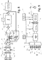
- FIG. 1 shows a block diagram of a system having an analog-to-digital converter device 11 according to an embodiment.
- the system of 1 has a signal source 10 which outputs an analog signal si.
- the analog signal si can have a relatively high frequency, for example greater than 1 MHz, greater than 3 MHz, or for example about 3.5 MHz, but is not limited to this.
- signal source 10 may be a sensor.
- the signal source 10 can be an inductive sensor, as will be described later with reference to FIG 2 is explained.
- the signal si can have a large dynamic range, for example at least a factor of 10 or at least a factor of 20 between the smallest amplitude (e.g. smallest voltage) and the largest amplitude (e.g. largest voltage).
- the signal si is fed directly to a demodulator 12 in the device 11 .
- direct means that no variable pre-amplification is carried out in order to adapt or reduce the dynamic range of the signal si.
- fixed amplification or other signal processing can be used, for example, within the signal source 10 be made.
- the demodulator mixes the signal si with a demodulation frequency fdemod to obtain a signal in a lower frequency band.
- demodulation techniques are known from the demodulation of communication signals, in which, for example, a high-frequency signal is converted into a baseband signal by a demodulator.
- the frequency fdemod can correspond to a mean frequency of the signal si.
- the demodulator 12 can be a passive demodulator.
- the demodulator 12 is followed by a time-continuous analog/digital converter 14, which has a chopper modulator 13 at its input and a chopper demodulator 15 at its output, which chop (chop) the signal according to a chopper frequency fchop.
- chopper techniques are used in particular for offset compensation of an offset of the analog/digital converter 14.
- fchop and fdemod are used below both to designate the signals and to designate the frequency of the signals.
- the frequency fchop can be adapted to the demodulation frequency fdemod.
- the frequency fdemod can be an integer multiple of the frequency fchop, pulses, rising edges or the like of the signal fdemod optionally being able to coincide with one of the pulses, rising edges and the like of the signal fchop.
- the frequency fdemod can be synchronized with a clock frequency fclock (corresponding to a sampling frequency fs) with which the analog/digital converter 14 works in such a way that fclock is an integer multiple of fdemod. This can help avoid beats.
- a time-continuous analog-to-digital converter is an analog-to-digital converter that does not work on the basis of individual sampled values at its input, but instead continuously processes signals present at its input, at least for specific periods of time. "At least for certain periods of time” means In this case, in some exemplary embodiments, which will be explained later, different inputs are processed alternately by means of multiplexing, with signals coming from an input only being processed in specific time intervals, but then being converted continuously over time within these time intervals. In this case, time-continuous analog-to-digital converters are also referred to as incremental converters. For the sake of simplicity, the term time-continuous analog-to-digital converter is primarily used below, it being understood that converters that only work continuously over time in some time sections, ie, for example, are incremental converters, can also be involved.
- inherent low-pass filtering is achieved by using a passive demodulator and/or a time-continuous analog-to-digital converter with chopping by chopper modulator 13 and chopper demodulator 15, so that no additional low-pass filter has to be provided.
- the combination of the time-continuous analog-to-digital converter 14 with the demodulator 12 makes it possible for the dynamic range to be sufficiently large for processing the signals, so that an amplifier with variable amplification does not have to be provided. The reasons for this will be explained in more detail later.
- the device 11 then outputs a digitized signal sdig, which can be further processed by downstream circuits.
- the signal source 10 is a sensor, for example, then the signal sdig represents the physical quantity detected by the sensor, and by evaluating the signal sdig, control processes or regulation processes can then be carried out, for example, on the basis of the physical quantity.
- Such analog-to-digital converter devices can be used, for example, in sensor systems that use inductive sensors.
- Such a sensor system according to an embodiment is in 2 shown.
- An inductive sensor of the system of 2 comprises an excitation coil 20, a moving inductance 21 and three receiving coils 22A, 22B and 22C.
- the moving inductance 21 can be implemented, for example, by a slotted metal disc which is attached to an element whose movement is to be measured.
- a rotor can be used, for example, of an electric motor, to which the inductor 21 is attached.
- Output currents Inu, Inv and Inw of the receiving coils 22A, 22B and 22C are received by a controller 23 and converted there by means of an analog-to-digital converter device of the controller 23 according to one exemplary embodiment, for example the analog-to-digital converter device 11 of the 1 or one of the analog-to-digital converter devices described below.
- the controller 23 has a digital signal processor (DSP) with which the digitized signals can optionally be further processed.
- the controller 23 has an oscillator (not shown) with which signals LCiop, LCiun for supplying the excitation coil 22 are output.
- the signals LCiop, LCiun are signals with a relatively high frequency, for example greater than 1 MHz or greater than 3 MHz, for example approximately 3.5 MHz.
- the leads to the excitation coil 20 are connected to ground through capacitors 24A, 24B as shown.
- the controller 23 is powered by a supply voltage 25 and is coupled to ground (gnd).
- the high frequency signal LCiop, LCiun which is applied to the excitation coil 20, is coupled into the receiver coils 22A, 22B, 22C by inductive coupling (i.e., by the action of the magnetic field generated by the excitation coil 20 on the receiver coils 22A, 22B, 22C).
- the strength of the coupling varies depending on the position of the inductor 21, for example depending on the angle of rotation of a rotor to which the inductor 21 is attached. This results in time-varying signals Inu, Inv and Inw, from which the position of the inductance 21 and thus of the moving element, for example the rotor, can be inferred.
- a correspondingly output signal sdig then represents the position of the moving element, for example the angular position of the rotor.
- inductive sensor is used as an example in several of the following exemplary embodiments. However, this is not to be understood as limiting, and other types of signal sources than inductive sensors can also be used in the exemplary embodiments described below.
- the 3 shows a system according to a further embodiment.
- a device for analog-to-digital conversion receives a signal from a receiving coil 30 at input pads 31A, 31B.
- the receiving coil 30 can be, for example, one of the receiving coils 22A, 22B and 22C of FIG 2 be.
- the signal from the receiving coil 30 is fed via input resistors 32A, 32B to a demodulator 30, which mixes the input signal with a frequency fdemod and thus demodulates it.
- the frequency fdemod can be used with the excitation frequency of an excitation coil such as the excitation coil 20 of 2 be synchronous and/or correspond to it.
- fdemod can correspond to a frequency fLC.
- fLC is a resonance frequency of an LC oscillation circuit generated by an excitation coil used, such as the excitation coil 20 of FIG 2 , together with external capacitances on the printed circuit board, eg 3.5MHz.
- a voltage zero crossing of the sinusoidal LC oscillation of the LC resonant circuit is taken to switch the digital fdemod frequency so that the frequency and phase match the demodulation.
- the input resistors 32A, 32B can have resistance values between 100 ⁇ and 1 M ⁇ , for example between 300 and 500 ⁇ , for example approximately 400 ⁇ .
- a voltage value which corresponds to the demodulated input signal is then present at a capacitor 34 and is time-averaged there. If the input amplitude of the signal received by the receiving coil 30 does not change, a DC mean value appears at the capacitor 34 plus a superimposed AC residual voltage, since the filtering of twice the modulation frequency (after rectification) is not particularly high. In contrast, the input signal is actually integrated at capacitors 310A and 310B, discussed below.
- Capacitors 35A and 35B represent capacitances to ground including parasitic capacitances.
- the Demodulation takes place in the embodiment of FIG 3 So as in the embodiment of 1 without amplification, especially without variable amplification.
- the input resistors 32A, 32B together with the capacitor 34 result in an RC filter which has a low-pass behavior. It is therefore not necessary to provide an additional low-pass filter, since low-pass filtering for filtering out high-frequency interference signals can be achieved in this way.
- fdemod can be an integer multiple of fchop.
- fdemod can be equal to the frequency fLC mentioned above.
- a chopped input voltage Vin is thus provided for a time-continuous sigma-delta analog-to-digital converter (CT- ⁇ - ⁇ -ADC) 37 .
- CT- ⁇ - ⁇ -ADC time-continuous sigma-delta analog-to-digital converter
- the continuous-time sigma-delta analog-to-digital converter 37 comprises an integrator using capacitors 310A, 310B. These capacitors 310A, 310B are connected to the rest of the converter via a chopper 39, which is also operated with the chopper frequency fchop.
- a current for example, is integrated at the capacitors 310A, 310B, which current is integrated by a voltage/current conversion in the input stage of the analog/digital converter 37 .
- a signal output by the time-continuous sigma-delta analog/digital converter 37 is also demodulated in a chopper demodulator 38 with the chopper frequency fchop, which in the digital case corresponds to a multiplication alternately by +1 and -1.
- the continuous-time sigma-delta analog-to-digital converter comprises, in some embodiments, as will be referred to later 8 will be explained in more detail, has a comparatively high input impedance, for example >100 ⁇ , for example in the range of 250 ⁇ , and has a feedback loop, as is usual with sigma-delta converters.
- a 6-bit signal with an output frequency of 10 MHz can be output as output signals, with other bit widths and frequencies also being possible.
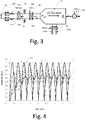
- the 4 shows the input signal for the chopper modulator 36 for different filter settings of the low-pass filter formed by the resistors 32A, 32B and the capacitor 34.
- the modulation frequency of the input signal (corresponding to the frequency of the excitation coil 20 of the 2 supplied signal LCiop, LCion) was assumed to be 3.5 MHz.
- Curve 40 shows a signal without capacitance 34, ie without low-pass filtering.
- a curve 41 shows a signal with a low-pass filter corner frequency of 3.5 MHz, and a curve 42 shows an example signal with a corner frequency of 1 MHz.
- a constant signal amplitude of the Receive coil 30 accepted.
- the signal oscillates around a stationary value which corresponds to the signal value to be converted.
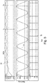
- FIG. 5 shows an example of an input signal for the demodulator 33, ie for a signal supplied by the receiving coil 30.
- FIG. A curve 52 shows an example of the signal with the frequency fdemod, which is fed to the demodulator 33.
- FIG. A curve 50 shows an input signal for the chopper 36, which was generated by the demodulation with filtering by the capacitor 34 and the resistors 32A, 32B.
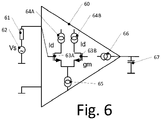
- the 6 a schematic circuit diagram of an input stage of a time-continuous analog-to-digital converter
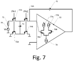
- the 7 shows a schematic circuit diagram of an input stage of an analog-to-digital converter with a switched input capacitor.
- a voltage source 62 represents the generation of an input voltage Vs for the converter. This is fed to an input amplifier 60, which has a transconductance gm.
- the input amplifier 60 is represented by a pair of transistors 63A, 63B, current sources 64A, 64B, which each generate a current Id, a current source 65 and a current source 66, which outputs the output signal of the amplifier 60. This representation is only to be understood as schematic.
- the output signal is integrated in an integration capacitance 67 having a value Cint.
- the inverse transconductance In order to generate low noise, the inverse transconductance must be 1/gm ⁇ the resistance value Rs of the input resistor 61. For example, a noise figure NF of +1 dB requires that the transconductance of the input stage satisfies the following relationship:
- the transistors 63A, 63B In order to optimize the noise, the transistors 63A, 63B must be operated in weak inversion in order to obtain the best possible ratio of gm to the current Id. In this case 1/gm becomes where n is set to 1.4 as the technology dependent factor by which the transistors are operated below threshold (i.e. in weak inversion), Id is the current through transistors 63A, 63B, k is the Boltzmann constant , T is the absolute temperature and q is the elementary charge. Room temperature was assumed as the temperature T for the printout on the right-hand side. For an input resistance Rs of 1 k ⁇ , Id must then be greater than about 110 ⁇ A, which is relatively easy to achieve for an input stage of a time-continuous sigma-delta analog-to-digital converter or an amplifier with an appropriate design.
- the 7 1 shows an input stage of an analog-to-digital converter with an input capacitor 73.
- An input voltage Vs is provided by a voltage source 79 via an input resistor 71.
- FIG. In a first phase of operation, transistor switches 72A, 72B are controlled closed by a signal Ph1, so that depending on the input voltage the input capacitor 73 is charged, while transistor switches 74A, 74B are open controlled by a signal Ph2. Then, in a second phase, the transistor switches 72A, 72B are opened and the transistor switches 74A, 74B are opened so as to transfer the charge to an input of an amplifier 70.
- the amplifier 70 has similar to the amplifier 60 of 6 an input transistor pair 76A, 76B with associated current sources 77A, 77B, 78. An output signal of the amplifier 70 is further processed (not shown) and fed back to an input of the amplifier 70 via a capacitor 75 . Again, the representation of 7 only to be understood as schematic.
- the dimensioning of a capacitance Cin of the input capacitor 73 is a challenge insofar as there are conflicting requirements here.
- the capacitance Cin must be chosen small enough for the converter to settle.
- the sampling frequency fs corresponding to a clock frequency fclock used for sampling, on which the signals Ph1, Ph2 are based must be much larger than the bandwidth of the signal to be modified.
- a be a multiple of a time constant ⁇ Rs ⁇ Cin, where Rs is the resistance value of the input resistor 71.
- Rs noise_equi 1 / fclock cint ⁇ 16.8 Rs
- Cint is the capacitance of capacitor 75 der 7 . This results in 16.8 times higher noise contribution from the impedance of the capacitors regardless of the clock frequency or the power supplied to the input transistors 76A, 76B.
- processing with time-continuous analog-to-digital converters can produce effects due to signal folding (aliasing), as is the case with analog-to-digital converters, which involve sampling with switched capacitors, for example, as in 7 use shown, may occur.
- This can reduce noise and image frequencies through signal folding and increase a dynamic range towards signals of smaller amplitudes.
- Image frequencies arise when signals with frequencies outside the useful frequency range are undesirably reflected in the useful frequency range. For example, an input interference signal around 3x fdemod+4kHz becomes visible as an additional undesired 4kHz signal after demodulation. Such effects can be reduced in embodiments.
- continuous-time analog-to-digital converters do not need a multiple of the above-mentioned time ⁇ within Ts/2 to settle. This reduces the bandwidth required for settling and thus the noise and the power required, since the greater the bandwidth required, the greater the electrical power required to achieve a required transient speed.
- Using choppers in conjunction with a continuous-time analog-to-digital converter can further reduce offset by one to three orders of magnitude.
- this combination can reduce flicker noise that rises towards lower frequencies and is caused by active electronic circuits and chopped resistors.
- even-numbered harmonic distortions can be reduced in some exemplary embodiments.
- the dynamic range can then also be increased upwards in time-continuous sigma-delta converters by multi-bit feedback or by feedback loops in order to compensate for offset ripples. Due to the increased dynamic range in various embodiments, no amplifier with variable gain is required, and direct passive demodulation with the demodulator 12 of FIG 1 or the demodulator 32 of 3 take place without such a variable amplifier being necessary. This may reduce offset that may be introduced by such an amplifier in some embodiments, reduce transient problems, and/or reduce noise in some embodiments.
- the combination of the input resistors 32A, 32B and the capacitor 34 can be used as a filter against electromagnetic interference (EMC filter, electromagnetic compliance) and can avoid intermodulation problems, which would arise from non-linearities of active switches such as amplification.
- EMC filter electromagnetic interference
- the input resistors 32A, 32B can also serve to protect against electrostatic discharges (ESD protection).
- ESD protection electrostatic discharges
- the input resistances can thus be well matched to noise conditions in continuous-time converters, and the signal processing can easily be adapted to a demanding noise figure, for example only an additional +1 dB as explained above.
- the vibrations that 4 are shown can, as shown, be reduced on the one hand by the low-pass filter properties of the time-continuous converter. At higher low-pass frequencies, an oscillation remains, the frequency of which is mainly determined by the clock frequency of the analog/digital converter fclock minus the frequency fLC mentioned above.
- FIG. 12 is in particular a non-limiting example of a structure for the continuous-time sigma-delta analog-to-digital converter 37 of FIG 3 shown.
- the analog to digital converter 8 has a voltage/current converter 80 (eg transconductance amplifier) into which a feedback signal of the analog/digital converter is fed back via an input resistor 81 .
- Output currents of the voltage/current converter 80 are taken by means of capacitors 310A, 310B analog integrated.
- the capacitors 310A, 310B can be implemented by means of gate oxides, for example.
- the current signal integrated in this way is fed to a comparator 82 .
- An output of the comparator is fed to the chopper demodulator 38, which in this case is arranged within the loop of the sigma-delta converter, but also effects the chopper demodulation of the output signal in this arrangement.
- the output of the comparator 82 which corresponds to a +1 or a -1, is fed to a digital integrator 83. This corresponds to a counter which counts up when the output of comparator 82 is +1 and counts down when the output of comparator 82 is -1.
- the output signal of the comparator 82 increased by +1 is added in an adder 84 to an output signal of the integrator 83 by means of a counter 85 .
- the adder 84 is a digital summation point which adds the digitally integrated value from the integrator 83 to the "faster" "proportional" or “forward” value from the comparator via 85.
- a fast immediate value from 85 is summed with a value from the integrator 83 delayed by integration.
- the path via 85 can be used as a stabilizing proportional forward path, similar to e.g. PID controllers or a stabilizing zero point in the Bode diagram in feedback systems be understood. Without the path 85, undesirable oscillations may occur in some applications.
- thermometer-encoded digital signal representing the input voltage Vin to the voltage/current converter 80 is generated.
- This signal can be converted to binary by a thermometer/binary encoder 86 Output signal to be converted.
- the thermometer-coded signal can be a 64-bit thermometer-coded signal, for example.
- thermometer-coded signal is also fed back into the voltage/current converter 80 via a digital-to-analog converter 87 as a feedback signal.
- the digital-to-analog converter 87 is a multi-bit digital-to-analog converter which feeds back the thermometer-coded 64-bit signal.
- a dynamic range of the sigma-delta analog-to-digital converter can be increased in some exemplary embodiments by such multi-bit digital-to-analog converters.
- sigma-delta analog-to-digital converter is only an example and other converters such as successive approximation register (SAR) converters, tracking converters (tracking ADCs) or other continuous-time converters can also be used.
- SAR successive approximation register
- tracking converters tilt ADCs
- continuous-time converters can also be used.
- a plurality of voltage/current converters 80 can also be provided, which can optionally be connected in parallel. In the case of small input signals in particular, this can increase the transconductance and thus reduce the noise.
- the parallel connection can only take place in the case of small input signals, for example with a voltage or current level below a predetermined threshold value, while only one voltage/current converter is used in the case of larger input signals. In this way, in combination with the chopping described, in some exemplary embodiments a corresponding amplification can be achieved even with small input signals, without causing significant offset and linearity errors as a result.
- a device as in 3 or as in 8 shown are provided.
- a single analog-to-digital converter device can be provided, which processes the various input signals alternately via a multiplexer 90 .
- An example of such a device is in 9 shown.
- Sense coil 30A is connected to input pads 31A, 31B of the illustrated analog-to-digital converter device, sense coil 30B is connected to input pads 31C, 31D, and sense coil 30C is connected to input pads 31E, 31F.
- the input pads 31A to 31F are connected to a multiplexer 90 which is arranged to select signals from one of the sense coils 30A to 30C for further processing.
- the multiplexer 90 is operated at a frequency fADC which determines at what time intervals the signals from the various sense coils 30A to 30C are switched over.
- the selected signal is supplied to a demodulator 92 whose function corresponds to the demodulator 33 of the 3 corresponds, with a corresponding demodulation signal having the frequency fdemod being supplied by an oscillator device 91 .
- a low-pass filter 93 is shown downstream of the demodulator 92, which can also be used as previously discussed embodiments by input resistances (e.g. 32A, 32B of 3 ) and a capacity (e.g. 34 der 3 ) can be formed.
- An output of the low-pass filter 93 is connected to an input of an incremental analog-to-digital converter 95 .
- the incremental analog-to-digital converter is essentially a continuous-time converter, but it only operates in continuous-time portions, namely portions during which the input signal from a sense coil 30A to 30C is processed.
- the incremental analog-to-digital converter 95 has a chopper modulator 96 at its input and a chopper demodulator 97, which is shown here at the output, but also as in FIG 8 shown may be located within the transducer.
- the converter types mentioned above can be used as the incremental analog/digital converter 95 .
- a SAR transducer can be used in combination with a tracking transducer.
- the low-pass filter 93 can also be an inherent low-pass filter of the analog-to-digital converter 95 .
- the low-pass filter and the incremental analog-to-digital converter are reset according to the frequency fADC at which the multiplexer 90 is operated, so that for each section in which the signal is processed by one of the receiving coils 30A to 30C, a "reboot" occurs.
- a previous value can be supplied to the incremental analog/digital converter 95 as a start value, which corresponds to an end value of a previous time segment for the respective receiving coil.
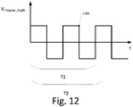
- prev can also be a predicted value derived from a previous history. This is with reference to the 13 explained.
- In 13 shows a curve with curve segments 1300A-C and 1301A-C a profile of an input signal to be digitized.
- the appropriate input signal is fed to the analog-to-digital converter (e.g. the input signal is a signal generated by receiving coil 30A and is selected via multiplexer 90), while in sections 1301A, 1301B and 1301C none Digitization occurs (e.g. because the signal of another receiving coil is selected by the multiplexer 90).
- the analog-to-digital converter e.g. the input signal is a signal generated by receiving coil 30A and is selected via multiplexer 90
- none Digitization occurs (e.g. because the signal of another receiving coil is selected by the multiplexer 90).
- a settling process is required for the digital output signal to settle to the correct value.
- prediction techniques are used, as indicated by arrows 1302A and 1302B. Not only the final value of the previous section is used here, but also a progression in one or more previous sections. For example, in a simple case, an average slope of the previous sections can be used to adjust a course and thus a starting value. In other embodiments, prediction techniques may be used. For example, a linear, quadratic or sinusoidal fit curve can be placed on previous sections and a starting value can be determined from this.
- an analog-to-digital converter can be switched between different modes or types of analog-to-digital converters. For example, at the beginning of each section 1300A, 1300B, 1300C, a SAR analog-to-digital conversion can first take place in order to quickly arrive at a corresponding starting value, and then, for example value tracking using a sigma-delta converter to reflect changes in the input value.
- a range selection device 94 can be provided, with which an input range for the incremental converter 95 can be selected via a signal RF, for example by setting a reference value.
- a range in which input signals can be converted can be increased.
- This selection of an input range is accomplished by an additional input to the incremental converter 95 as shown, rather than by error prone additional circuitry upstream of the incremental converter 95 input stage such as a variable gain amplifier as in some prior art approaches.
- offset errors can thus be reduced, and unavoidable offset noise and settling processes in upstream chopped or non-chopped amplifiers are avoided.
- Such range switching can be achieved in a simple manner by transconductance switching of the input stage of the incremental converter 95.
- the voltage-to-current conversion of the input stage can therefore be switched by factors.
- the full-scale range of a digital-to-analog converter can be switched in a feedback path of the incremental converter 95 (see previous exemplary embodiments) or a reference of the digital-to-analog converter. This also causes a scale change of LSB/V (least significant bits per volt input voltage) at the output of the incremental converter 95.
- LSB/V least significant bits per volt input voltage
- chopper ripple also known as chopper ripple
- Such ripples can be compensated for by feedback paths.
- a corresponding embodiment is in 10 shown.
- a first input signal is fed via input pads 31A, 31B, and fed from there via input resistors 32A, 32B to a demodulator 33A, which runs at a frequency fdemod and the demodulator 33 of the 3 is equivalent to.
- Downstream of the demodulator 33A is a capacitance arrangement 1000A, the function of which is the capacitance 34 and the capacitances 35A, 35B 3 is equivalent to.
- a second input signal can be fed via pads 31C, 31D and input resistors 32C, 32B to a demodulator 33B, which is followed by a capacitance arrangement 1000B.
- the signals processed in this way are fed to a combined multiplexer and chopper modulator, the multiplexer function having the reference number 1001 and the chopper modulator function corresponding to FIG 3 indicated by the reference numeral 36.
- the function of the chopper modulator is essentially a multiplication by +1 or -1, which corresponds to an optional swapping of the inputs. In order to additionally integrate a multiplexer function, this swapping can be applied to all inputs (in the case of the 10 ) to be expanded.
- the multiplexer is doing with a frequency fADC according to the 7 operated, and the modulator (that is, swapping the lines) with a frequency fchop.
- the signals are then converted with a time-continuous sigma-delta analog-to-digital converter whose structure initially corresponds to that of 8 and corresponding elements bear the same reference numerals.
- An integrator 1002 which is operated at a frequency Fclkl, essentially corresponds to the integrator 83 of FIG 8 and can be implemented as an up/down counter, for example. Elements 84 and 85 of 8 can also be provided here. In the embodiment of 10 a notch filter 1003 is also provided at the output.
- the first feedback path 1011 essentially corresponds to the feedback of FIG 8 , wherein an addition 1005 corresponds to the addition 85 and an adder 1006 to the adder 84, so that an output of the adder 1006 has a thermometer-coded signal.
- This signal is chopped in a chopper modulator 1007 with the chopper frequency fchop and fed to an adder 1008 .
- the second feedback path 1012 comprises a demodulation device 1009 together with a digital sigma-delta modulator 1010.
- the demodulation 1009 performs a two-phase demodulation based on the chopper frequency and together with the digital sigma-delta modulator 1010 generates an offset signal, for example a four-bit offset signal that at least partially compensates for ripples caused by chopping.
- This technique is known per se.
- the signal supplied to the digital-to-analog converter 87 thus also contains a component which compensates for ripples caused by the chopping.
- Optional bit rotation 1013 can further reduce offsets through dynamic element matching techniques. Bit rotation is one of many ways, known per se, of compensating for the non-linearity of converters on average over time. Other conventional methods can also be used for this purpose.
- a reference current, an amplifier, or a resistance of a detection resistor 81 for range selection can be restricted.
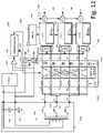
- the receiving coils 22A, 22B and 22C already discussed and an excitation coil 20 are provided.
- the inductance 21 is not shown and is only represented by a transformer coupling symbol in FIG 11 represented.
- the excitation coil 20 is supplied with an excitation signal from an oscillator 1101, the already capacitors 24A, 24B discussed are provided on the lines from the oscillator 1101 to the excitation coil 20.
- the excitation coil 20, the receiving coils 22A to 22C and the capacitors 24A, 24B can be provided on a circuit board 1100, for example.
- the output signals Inu, Inv and Inw are applied to a filter/demodulation arrangement 1102 as shown.
- the device 1102 includes an array of input resistors 1103, with each channel (LN0, LN1, LN2) being assigned two input resistors whose function is that of the input resistors 32A, 32B of the 8 is equivalent to.
- the input resistance arrangement 1103 downstream is a multiplexer and demodulation arrangement 1104, which is controlled by a frequency fdemod and initially the function of the demodulator 33 of 3 executes
- the multiplexer and demodulator arrangement 1104 switches the corresponding input channels (LNu, LNv, LNw) to corresponding output signals UP, UN; VP, VN; WP, WN. This can be done with a fixed assignment. However, the assignment can also change in order to achieve dynamic device assignment (dynamic element matching).
- a capacitor arrangement 1105 at the output of the multiplexer and demodulator arrangement 1104 is followed by a capacitance arrangement 1105 whose function corresponds to the capacitances 34, 35A, 35B of the 3 or the capacitor arrangements 1000A, 1000B of 10 is equivalent to.
- a separate path for digitization is then provided for each pair of output signals (UP, UN; VP, VN; WP, WN) of the arrangement 1102 .
- the figures 9 and 10 a parallel processing. This generally requires more chip area, but is faster with the same implementation of the analog-digital converter and the same clocking, since all signals are converted in parallel.
- Each path comprises a chopper modulator 36A, 36B, 36C, a continuous-time sigma-delta analog-to-digital converter 37A, 37B, 37C and a digital chopper demodulator 38A, 38B, 38C, which are functionally similar to the corresponding elements 36, 37, 38 of the 3 correspond to.
- Each continuous-time sigma-delta analog-to-digital converter 37A, 37B, 37C like the continuous-time sigma-delta analog-to-digital converter 37 of 3 Integrator capacitors and, which are chopper-connected to the rest of the converter, such as elements 39, 310A and 310B of FIG 3 , exhibit. These are in 11 not shown separately.
- the chopper frequency fchop can be synchronized with the demodulator frequency fdemod.
- the demodulator frequency fdemod is synchronized with the excitation frequency that is supplied to the excitation coil 20 .
- a dynamic element assignment (dynamic element matching) can also take place between the respective elements 36A to 36C, 37A to 37C and 38A to 38C, so that the signals of a channel with different combinations of chopper modulator, time-continuous sigma-delta analog-digital converter and chopper demodulator can be processed. Digital output signals u, v and w can then be further processed.
- a range selection here denoted by reference numeral 1109, can also be provided for each of the time-continuous analog-to-digital converters 37A, 37B and 37C.
- the signal from the oscillator 1101 is fed via a phase comparator 1108 to a phase adjustment device 1106, which then generates the signal fdemod synchronized with the output signal of the oscillator 1101.
- the oscillator signal itself can be demodulated by a demodulator 1107.
- An output of the demodulator 1107 can then be used to determine serve the amplitude of the oscillator signal.
- the frequency fdemod can be determined by measuring the amplitude on the basis of zero crossings of the oscillation with the frequency fLC through the excitation coil 20 and parasitic capacitances.
- the resistance arrangement 1103 and the capacitance arrangement 1105 can in turn together form a low-pass filter function.
- the resistor arrangement 1103 can serve to protect against electrostatic discharges (ESD protection).
- Such dynamic element allocation may occur during operation, during initial calibration, or during device startup.
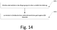
- the 14 shows a flowchart for illustration. The method can be used with the devices described above and systems and will be described for simplicity with reference to the embodiments described above. The application of the method of 14 however, is not implemented on the embodiments described above.
- the method includes direct demodulation of an input signal to be converted without variable amplification, in particular passive demodulation with a mixer that is operated at a demodulation frequency fdemod.
- the demodulation can include low-pass filtering, for which purpose input resistances and a capacitance arrangement connected downstream of the demodulator can be used, as described above.
- the input resistances can also be used to protect against electrostatic discharges.
- the signal demodulated in this way is converted from analog to digital in a time-continuous manner, at least in time segments, with chopper modulators and chopper demodulators being used, as was described above.
- "At least in periods of time” means, as already explained, in particular that it is a single time-continuous analog-to-digital converter as in 3 , separate time-continuous analog-to-digital converters for each channel as in 11 or also multiplexed incremental analog-to-digital converters as in FIGS 9 and 10 can act. Variations and modifications, which have been described above for the devices, are correspondingly also applicable to the method of FIG 14 applicable.
- the different frequencies such as the demodulation frequency, the excitation frequency, the chopper frequency or a switching frequency of a multiplexer fADC as described above be synchronized, there may be feedback to reduce ripple as in 10 can be applied, multiplexing can be applied or dynamic element allocation can be used.
- This enumeration is not to be regarded as exhaustive, and all the variations and additions described above can also be applied to the method in a corresponding form.
- demodulation takes place by means of a demodulator at a demodulation frequency fdemod and, on the other hand, chopping at a chopper frequency fchop.
- a continuous-time analog-to-digital converter in particular a sigma-delta analog-to-digital converter, with inherent chopper and demodulation function is used.
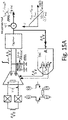
- the Figure 15A shows a system with a device for analog-to-digital conversion according to an embodiment.
- the device for analog-to-digital conversion receives the Figure 15A a signal from a receiving coil 30 to input pads 31A, 31B.
- a voltage/current converter 80 which is essentially as already described with reference to FIGS 8 corresponds to the voltage/current converter 80 described above.
- there is no demodulator and no chopper here so that the input voltage applied to the pads 31A, 31B Vin is fed directly to the current/voltage converter 80 already discussed.
- the integrator capacitances 310A, 310B already discussed are connected downstream of the current/voltage converter 80 via the chopper 39 .
- Capacitance values of the integrator capacitances 310A, 310B can be in the range of 5 to 30pF. In the embodiment of Figure 15A the capacitors 310A, 310 can have smaller capacitance values than in the 3 , for example by a factor of 10 smaller capacitance values.
- the chopper 39 is operated with a chopper frequency fchop which, in contrast to the previous exemplary embodiments, corresponds to the required demodulation frequency fdemod.
- this demodulation frequency fdemod results from a mean frequency of the signal received by the receiving coil 30 .
- this achieves an integration, together with a resistance of the current/voltage converter 80, RC filtering, chopping and demodulation.
- the current/voltage converter 80 is in Figure 15B shown schematically, the input voltage Vin being present at the gate terminals of transistors 1504, 1505 and the output signal being generated via current sources 1502, 1503, 1507, 1508.
- the inside Figure 15A shown resistance of the current / voltage converter 80 corresponds to a resistor 1506 of Figure 15B and may, for example, be of the order of 400 ⁇ , while the drain current of transistors 1504, 1505 may be in excess of 200 ⁇ A.
- the analog integrated, demodulated and chopped signal is converted into a digital signal by a Digitizer 1500.
- this digitizer 1500 can include a comparator.
- the digitized signal is then multiplied alternately by +1 and -1 by a multiplier 1501 according to the chopper frequency fchop (which in turn corresponds here to the demodulation frequency fdemod) in order to generate a digital output signal digout.
- the digital output signal digout is fed back via a digital-to-analog converter 87, as already referred to in FIG 8 explained.
- Figure 15A signal waveforms are also shown schematically for illustration. As indicated at the output of digout, the amplitude of the digital output signal depends on the frequency with which the system of the Figure 15A and in particular the digitizer 1500 is operated, and on the capacitance values Cinteg of the capacitors 310A, 310B.
- the Figure 15C shows a differential voltage between the integrator capacitances 310A and 310B over the frequency and also shows different frequency values, namely the frequency at which the converter is operated, the chopper frequency equal to the demodulation frequency and a frequency Gm/2n Cinteg, which results from the transconductance Gm of the voltage - / current transformer 80 and the capacitance value Cinteg results.
- the transconductance corresponds to the reciprocal of the resistance value of the resistor 1506 of the voltage/current converter 80.
- an inherent chopper and demodulation function can be achieved with a continuous-time analog-to-digital converter without having to provide a demodulator and chopper at the input of the voltage-to-current converter 80 .
- This can reduce device noise and save power and chip area, as well as increase accuracy.
- signal folding effects and offset errors can be reduced.
- the RC filtering provided by resistor 1506 and capacitors 310A, 310B can improve electromagnetic compatibility.
- a corresponding system can also be set up using an operational amplifier, ie the signal integration is better to be considered in the voltage range than integration of a current on capacitors.
- FIG 16A A corresponding exemplary embodiment is shown in FIG 16A .
- the voltage/current converter 80, the chopper 39 and the capacitors 310A, 310B are replaced by an arrangement with an operational amplifier 1600, the inputs of which are connected to the pads 31A, 31B via input resistors 32A, 32B.
- a resistance of resistors 32A, 32B may be on the order of 400 ⁇ .
- switched capacitors 1602A, 1602B are provided in the feedback paths of the operational amplifier 1600 as shown, which can be optionally connected to the inputs or outputs of the operational amplifier 1600 using changeover switches 1601A to 1601D.
- the changeover switches 1601A to 1601D are operated with the chopper frequency fchop, which in turn is as in the exemplary embodiment of FIG Figure 15A is equal to the demodulation frequency fdemod.
- An equivalent circuit of the operational amplifier 1600 is in Figure 16B shown with current sources 1603, 1604 and 1607 and input transistors 1605, 1606 to the gates of which the input voltage from pads 31A, 31B is applied through resistors 32A, 32B.
- the embodiment corresponds to 16A the one who Figure 15A , the output of the digital-to-analog converter being fed back here to the inputs of the operational amplifier 1600.
- An RC filter is formed here by the resistors 32A, 32B and the capacitors 1602A, 1602B. Also here is through the capacitances 1602A, 1602B implement an integrator function. In addition, chopping and demodulation take place, similar to those already used for the Figure 15A explained.
- an additional RC filter can be provided, for example to improve the electromagnetic compatibility, which can be dimensioned smaller than in devices that have no integrated RC filtering by integration capacitors.
- the embodiment of 16A can at higher temperatures advantages over the embodiment of the Figure 15A exhibit.
- the demodulation frequency in the embodiments of Figure 15A and 16A is equal to the chopper frequency, synchronized in some embodiments with a mean frequency of a signal received by the receiving coil 30 and with a frequency fADC at which the analog-to-digital converter is operated and the digital signal is output.
- the digitizer 1500, the comparator 82, the digital integrator 83, the thermometer/binary coder 86 and the digital-to-analog converter 87 are controlled with the frequency fADC. Examples of such synchronization are in Figures 17A to 17C shown.
- an LC oscillator 1701 generates a signal which is fed via pads 1700A, 1700B to the devices already referred to in FIG 2 described excitation coil 20, with the also with reference to the 2 described capacitors 24A, 24B is coupled, is output.
- the signal generated by the LC oscillator 1701 is also fed to a phase locked loop (PLL) 1702 which produces the chopper frequency fchop equal to fdemod, the frequency fADC and the frequency fdig via an oscillator and divider 1703 (referred to herein as ADC oscillator/divider).
- fADC can also equal fchop.
- fADC can be generated from fdig by frequency division.
- fdig can be 40MHz and fADC can be 10MHz. fdig thus serves as the basis for the generation of fADC.
- fADC and fdig are thus synchronized to the excitation frequency that the LC oscillator 1701 generates for the excitation coil 20, in that the output signal of the LC oscillator 1701 is fed to the phase-locked loop 1702 as a reference, which in turn controls the ADC oscillator 1703 becomes.
- a controllable LC oscillator 1704 is provided, which can contain, for example, a variable capacitance as shown.
- This capacitance is regulated via a digital PLL 1705 in such a way that the frequency generated by the LC oscillator 1704 is regulated to a frequency generated by the ADC oscillator 1703, which is fed to the digital PLL 1705 as a reference frequency.
- the ADC oscillator 1703 is controlled as a function of the frequency of the LC oscillator 1701 via the PLL 1702, is in the Figure 17B the reverse path has been taken, namely that the frequency of the LC oscillator 1704 is controlled via the digital PLL 1705 to the frequency of the ADC oscillator 1703.
- the frequencies fchop, fADC and fdig can then also be generated by means of frequency dividers that are connected to the ADC oscillator 1703.
- the reference frequency mentioned above can also be frequency divided, eg a frequency divided version of fdig.
- FIG. 17C A variant of Figure 17B is in the Figure 17C shown.
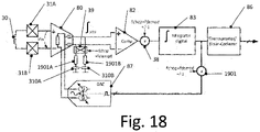
- the 18 shows a variation of the embodiment of FIG Figure 15A .
- the capacitors 310A, 310B are preceded by resistors 1901A, 1901B.
- the resistors 1901A and 1902B cause a zero in the transfer function of the device, which in some embodiments causes an uncontrolled ringing of the analog-to-digital converter loop, in the case of the 18 essentially a sigma delta loop, analog integrator (through the integrator capacitances 310A, 310B), a digital integrator 83 and the digital to analog converter 87.
- the phase after the 2 integrators in the loop can be -180°, which in some cases could mean uncontrolled ringing in the feedback.
- the zero through the inserted resistors 1901A, 1901B is able to reduce this phase or in other words to increase the phase margin.
- the digitizer 1500 the Figure 15A similar to that 8 implemented by a comparator 82, a digital integrator 83 and a thermometer/binary encoder 86.
- the multiplier 1501 of the Figure 15A is implemented here by a first multiplier 38 between the comparator 82 and the digital integrator 83 and a second multiplier 1901 in a feedback path to the digital-to-analog converter 87 already discussed.
- the counter 85 and the adder 84 can be provided in parallel with the digital integrator 83, as with reference to FIG 8 described.
- the 19 shows another embodiment, which the embodiment of 18 supplemented by feedback to eliminate offset ripples (ripples) 2000.
- a signal is filtered before or after the multiplier 38 and added to the input of the digital-to-analog converter 87 by means of an adder 2001 in order to eliminate ripples arising from chopping and the like.
- This can essentially be as already mentioned with reference to 10 explained happen.
- Further implementations and further information on such feedback to eliminate chopper-induced ripples are also in the German patent application DE 10 2020 111 914.3 to be taken from the applicant
- chopping eliminates an offset, which is a DC offset, but creates AC ripple in the output signal. This is compensated for by the additional digital offset ripple feedback 2000.
- FIG. 12 shows a modification of the embodiment of FIG 16A .
- the digitizer 1500 and the multiplier 1501 as in the 19 implemented by comparator 82, multiplier 38, digital integrator 83, thermometer/binary encoder 86 and multiplier 1901.
- the 19 implements the digital offset ripple feedback 2000 with the adder 2001.
- the embodiment of the 20 switchable input resistors 2101A, 2101B or 2102A, 2102B it being possible for the resistors 2101A, 2101B to be activated and deactivated by means of switches 2100A, 2100B.
- the resistors 2101A, 2102B can have resistance values that are lower by a factor of 10 than the resistors 2102A, 2102B, so that when the switches 2100A, 2100B are closed, the resistors 2101A, 2101B determine the total input resistance.
- resistors 2101A, 2101B can have resistance values of approximately 400 ohms
- resistors 2102A, 2102B can have resistance values of, for example, 4 k ⁇ . In this way it is possible to switch between different input signal ranges.
- the various modifications of 20 compared to the 16A (Implementation of the digitizer, digital offset ripple feedback and switchable input resistances) can be implemented independently of each other, even if they are in the 20 are shown together.
- the 21 shows a variant of the embodiment of FIG 20 .
- an analog offset ripple feedback 2201 is provided here, which additionally acts on the inputs of the operational amplifier 1600 as a function of signals tapped off at the input of the comparator 82.
- a digital-to-analog converter 2200 is provided, which has switchable resistors that can be connected to an input voltage or a reference voltage.
- Such a digital-to-analog converter is also used in conventional structures together with operational amplifiers instead of current-controlled digital-to-analog converters such as the digital-to-analog converter 87 .
- These variants can also be implemented independently of one another.
- the 22 shows a modification of 19 .
- the digital offset ripple feedback 2000 with which the input of the digital-to-analog converter 87 is applied via the adder 2001
- the output of the digital offset ripple feedback 2000 via a separate analog-to-digital converter 2300 dem Voltage / current converter 80 supplied.
- a chopper 2301 is then provided at the output of the digital/analog converter 87.
Abstract
Es werden Vorrichtungen und Verfahren zur Analog-DigitalWandlung und entsprechende Systeme mit einem Sensor und einer derartigen Vorrichtung bereitgestellt. Dabei erfolgt eine Demodulation ohne variable Vorverstärkung gefolgt von einer zumindest in Zeitabschnitten zeitkontinuierlichen Analog-Digital-Wandlung, welche zudem Choppertechniken benutzt.Devices and methods for analog-to-digital conversion and corresponding systems with a sensor and such a device are provided. In this case, demodulation takes place without variable pre-amplification, followed by analog-to-digital conversion, which is continuous at least in time segments and also uses chopper techniques.
Description
Die vorliegende Anmeldung betrifft Vorrichtungen zur Analog-Digital-Wandlung, Sensorsysteme, die derartige Vorrichtungen zur Wandlung eines von einem Sensor ausgegebenen Analogsignals aufweisen, sowie entsprechende Verfahren.The present application relates to devices for analog-to-digital conversion, sensor systems that have devices of this type for converting an analog signal output by a sensor, and corresponding methods.
In vielen Anwendungen wird ein analoges Signal in ein digitales Signal gewandelt, und dann digital weiter verarbeitet. Ein Beispiel sind Sensoranwendungen, bei denen mittels eines Sensors eine physikalische Größe, beispielsweise Geschwindigkeit, Position und dergleichen, erfasst wird, ein entsprechendes analoges Signal von dem Sensor ausgegeben wird und dann in ein digitales Signal gewandelt wird, um weiterverarbeitet zu werden.In many applications, an analog signal is converted into a digital signal and then further processed digitally. An example are sensor applications in which a physical variable, for example speed, position and the like, is detected by means of a sensor, a corresponding analog signal is output by the sensor and then converted into a digital signal in order to be processed further.
In manchen Fällen kann das zu wandelnde Analogsignal einen relativ hohen Dynamikbereich, beispielsweise hinsichtlich einer Spannung des Signals, aufweisen. Ein Beispiel für Sensoren, die einen derartigen hohen Dynamikbereich in ihrem Ausgangssignal aufweisen können, sind induktive Bewegungssensoren. Bei solchen Sensoren wird durch zuführen eines Anregungssignals an eine Anregungsspule ein hochfrequentes Magnetfeld erzeugt. Mittels mehrerer Detektionsspulen wird das Magnetfeld gemessen. Die magnetische Kopplung zwischen Anregungsspule und Detektionsspulen hängt dabei beispielsweise von einer Position eines Rotors, welcher mit einer Induktivität versehen ist, ab. Das Anregungssignal kann dabei eine Frequenz im Bereich von 3,5 MHz aufweisen. Eine von den Empfangsspulen ausgegebene Spannung kann beispielsweise in einem Bereich zwischen 4 und 120 mV liegen, was einem Faktor 30 zwischen der kleinsten und größten Spannung entspricht. Zusammen mit der hohen Frequenz (beispielsweise 3,5 MHz) stellt dies eine Herausforderung für die nachfolgende Demodulation (Konvertierung des Sensorsignals auf eine niedrigere Frequenz) und Analog-Digital-Wandlung dar.In some cases, the analog signal to be converted can have a relatively high dynamic range, for example with regard to a voltage of the signal. An example of sensors that can have such a high dynamic range in their output signal are inductive motion sensors. In such sensors, a high-frequency magnetic field is generated by feeding an excitation signal to an excitation coil. The magnetic field is measured by means of several detection coils. The magnetic coupling between the excitation coil and the detection coil depends, for example, on the position of a rotor, which is provided with an inductor. The excitation signal can have a frequency in the range of 3.5 MHz. A voltage output by the receiving coils can, for example, be in a range between 4 and 120 mV, which is a
Bei herkömmlichen Herangehensweisen werden ein oder mehrere Verstärker mit variabler Verstärkung (AGC, adjustable gain control) verwendet. Je nach Pegel des Eingangssignals wird die variable Verstärkung eingestellt, um so ein von einem Analog-Digital-Wandler letztendlich zu wandelndes Signal mit einem reduzierten Dynamikbereich bereitzustellen. Derartige Verstärker werden häufig mit Tiefpassfiltern kombiniert, um Signalfaltungseffekte (aliasing) zu unterdrücken und unerwünschte hochfrequente Komponenten herauszufiltern. Derartige Tiefpassfilter benötigen eine entsprechende Chipfläche. Auch Verstärker mit variabler Verstärkung benötigen entsprechenden Platz auf dem Chip und erhöhen den Stromverbrauch.Conventional approaches use one or more variable gain control (AGC) amplifiers. Depending on the level of the input signal, the variable amplification is set in order to provide a signal with a reduced dynamic range that is ultimately to be converted by an analog-to-digital converter. Such amplifiers are often combined with low-pass filters to suppress signal aliasing effects and to filter out unwanted high-frequency components. Such low-pass filters require a corresponding chip area. Amplifiers with variable gain also require corresponding space on the chip and increase power consumption.
Andere herkömmliche Herangehensweisen benötigen Kanalfilter, um Frequenzen außerhalb eines Nutzfrequenzbereichs (beispielsweise die erwähnten 3,5 MHz) herauszufiltern, und/oder Puffer vor einer Analog-Digital-Wandler-Schaltung, welche zu Offsetfehlern und zusätzlichem Stromverbrauch führen können.Other conventional approaches require channel filters to filter out frequencies outside of a useful frequency range (e.g. the mentioned 3.5 MHz) and/or buffers in front of an analog-to-digital converter circuit, which can lead to offset errors and additional power consumption.
Es werden eine Analog-Digital-Wandler-Vorrichtung nach Anspruch 1, ein System nach Anspruch 12 sowie ein Verfahren nach Anspruch 15 bereitgestellt. Die Unteransprüche definieren weitere Ausführungsformen.An analog-to-digital converter device according to
Gemäß einem Ausführungsbeispiel wird eine Vorrichtung zur Analog-Digital-Wandlung bereitgestellt, umfassend:
- einen Demodulator zum Demodulieren eines Eingangssignals mit einem Demodulationssignal, welches eine Demodulationsfrequenz aufweist, ohne variable Vorverstärkung, einen dem Demodulator nachgeschalteten Choppermodulator zum Choppen auf Basis eines Choppersignals,
- einen dem Choppermodulator nachgeschalteten zumindest in Zeitabschnitten zeitkontinuierlichen arbeitenden Analog-Digital-Wandler, und
- einen Chopperdemodulator zum Choppen auf Basis des Choppersignals.
- a demodulator for demodulating an input signal with a demodulation signal, which has a demodulation frequency, without variable preamplification, a chopper modulator connected downstream of the demodulator for chopping on the basis of a chopper signal,
- an analog-to-digital converter which is connected downstream of the chopper modulator and operates continuously at least in time segments, and
- a chopper demodulator for chopping based on the chopper signal.
Gemäß einem weiteren Ausführungsbeispiel wird eine Vorrichtung zur Analog-Digital-Wandlung bereitgestellt, umfassend:
einen zumindest in Zeitabschnitten zeitkontinuierlichen arbeitenden Analog-Digital-Wandler, welcher aufweist:
- mindestens eine Integratorkapazität, die mit dem übrigen Analog-Digital-Wandler in Abhängigkeit von einem Choppersignals verbunden ist, wobei das Choppersignal eine Frequenz aufweist, die gleich einer Demodulationsfrequenz zum Demodulieren eines Eingangssignals der Vorrichtung ist, und
- einen Chopperdemodulator zum Choppen auf Basis des Choppersignals.
an analog-to-digital converter that operates continuously at least in time segments, which has:
- at least one integrator capacitance connected to the remainder of the analog-to-digital converter in response to a chopper signal, the chopper signal having a frequency equal to a demodulation frequency for demodulating an input signal of the device, and
- a chopper demodulator for chopping based on the chopper signal.
Gemäß einem weiteren Ausführungsbeispiel wird ein System bereitgestellt, umfassend:
- einen Sensor, und
- eine Vorrichtung zur Analog-Digital-Wandlung wie oben beschrieben zum Verarbeiten eines Signals von dem Sensor.
- a sensor, and
- an analog to digital conversion device as described above for processing a signal from the sensor.
Gemäß noch einem weiteren Ausführungsbeispiel wird ein Verfahren zur Analog-Digital-Wandlung bereitgestellt, umfassend:
- direktes Demodulieren eines Eingangssignals ohne variable Vorverstärkung, und
- zumindest in Zeitabschnitten zeitkontinuierliches Analog-Digital-Wandeln des demodulierten Eingangssignals mit Choppermodulation und Chopperdemodulation.
- directly demodulating an input signal without variable gain, and
- at least in time segments, time-continuous analog-to-digital conversion of the demodulated input signal with chopper modulation and chopper demodulation.
Gemäß einem weiteren Ausführungsbeispiel wird ein Verfahren zur Analog-Digital-Wandlung bereitgestellt, umfassend zumindest in Zeitabschnitten zeitkontinuierliches Analog-Digital-Wandeln eines Eingangssignals, wobei das zumindest in Zeitabschnitten zeitkontinuierliches Analog-Digital-Wandeln ein Betreiben von Integratorkapazitäten basierend auf einem Choppersignal umfasst, wobei das Choppersignal eine Chopperfrequenz aufweist, die gleich einer Demodulationsfrequenz zum Demodulieren eines zu wandelnden Eingangssignals ist.According to a further exemplary embodiment, a method for analog-to-digital conversion is provided, comprising analog-to-digital conversion of an input signal that is continuous in time at least in time segments, wherein the analog-to-digital conversion that is continuous in time at least in time segments includes operating integrator capacitances based on a chopper signal, wherein the chopper signal has a chopper frequency equal to a demodulation frequency for demodulating an input signal to be converted.
Die obige Kurzfassung stellt lediglich einen kurzen Überblick über manche Ausführungsformen dar und ist nicht als einschränkend auszulegen. Insbesondere können andere Ausführungsformen andere Merkmale als die oben genannten aufweisen.The summary above is merely a brief overview of some embodiments and is not intended to be limiting. In particular, other embodiments may have features other than those mentioned above.
-
Fig. 1 ist ein Blockdiagramm eines Systems gemäß einem Ausführungsbeispiel.1 12 is a block diagram of a system according to one embodiment. -
Fig. 2 ist ein Diagramm eines Systems gemäß einem Ausführungsbeispiel.2 12 is a diagram of a system according to one embodiment. -
Fig. 3 ist ein Schaltungsdiagramm eines Systems gemäß einem Ausführungsbeispiel.3 12 is a circuit diagram of a system according to an embodiment. -
Fig. 4 zeigt Beispielsignale zur Veranschaulichung der Funktionsweise von manchen Ausführungsbeispielen.4 shows sample signals to illustrate the functionality of some embodiments. -
Fig. 5 zeigt Beispielsignale zur Veranschaulichung der Funktionsweise von manchen Ausführungsbeispielen.figure 5 shows sample signals to illustrate the functionality of some embodiments. -
Fig. 6 zeigt ein schematisches Schaltungsdiagramm eines zeitkontinuierlichen Analog-Digital-Wandlers zur Erläuterung mancher Ausführungsbeispiele.6 shows a schematic circuit diagram of a time-continuous analog-to-digital converter to explain some exemplary embodiments. -
Fig. 7 zeigt ein vereinfachtes Schaltungsdiagramm eines Analog-Digital-Wandlers mit geschalteten Eingangskondensator als Vergleichsbeispiel zurFig. 6 .7 shows a simplified circuit diagram of an analog-to-digital converter with a switched input capacitor as a comparison example6 . -
Fig. 8 zeigt ein Schaltungsdiagramm eines Systems gemäß einem Ausführungsbeispiel.8 12 shows a circuit diagram of a system according to an embodiment. -
Fig. 9 zeigt ein Schaltungsdiagramm eines Systems gemäß einem Ausführungsbeispiel.9 12 shows a circuit diagram of a system according to an embodiment. -
Fig. 10 zeigt ein Schaltungsdiagramm eines Systems gemäß einem Ausführungsbeispiel.10 12 shows a circuit diagram of a system according to an embodiment. -
Fig. 11 zeigt ein Schaltungsdiagramm eines Systems gemäß einem Ausführungsbeispiel.11 12 shows a circuit diagram of a system according to an embodiment. -
Fig. 12 zeigt ein Diagramm mit Signalen zur Veranschaulichung mancher Ausführungsbeispiele.12 shows a diagram with signals to illustrate some embodiments. -
Fig. 13 ist ein Diagramm zur Veranschaulichung der Vorhersage eines nächsten Startwertes.13 Figure 12 is a chart illustrating prediction of a next seed. -
Fig. 14 ist ein Flussdiagramm zur Veranschaulichung von Verfahren gemäß mancher Ausführungsbeispiele.14 FIG. 12 is a flow chart illustrating methods according to some example embodiments. -
Fig. 15A ist ein Schaltungsdiagramm eines Systems gemäß einem Ausführungsbeispiel.Figure 15A 12 is a circuit diagram of a system according to an embodiment. -
Fig. 15B veranschaulicht einen Spannungs/Stromwandler derFig. 15A .Figure 15B illustrates a voltage/current converter of FIGFigure 15A . -
Fig. 15C ist ein Diagramm zur Veranschaulichung des Systems derFig. 15A .Figure 15C is a diagram illustrating the system ofFigure 15A . -
Fig. 16A ist ein Schaltungsdiagramm eines Systems gemäß einem Ausführungsbeispiel.16A -
Fig. 16B veranschaulicht einen Operationsverstärker derFig. 16A .Figure 16B illustrates an operational amplifier of16A . -
Fig. 17A bis 17C zeigen verschiedene Ausführungsbeispiele zur Synchronisierung von Signalen.Figures 17A to 17C show various exemplary embodiments for synchronizing signals. -
Fig. 18 bis 22 sind Schaltungsdiagramme von Systemen gemäß verschiedener Ausführungsbeispiele.Figures 18 to 22 10 are circuit diagrams of systems according to various embodiments.
Im Folgenden werden verschiedene Ausführungsbeispiele detailliert erläutert. Diese Ausführungsbeispiele sind nicht als einschränkend auszulegen, sondern dienen lediglich der Veranschaulichung. Beispielsweise werden manche Ausführungsbeispiele mit einer Vielzahl von Merkmalen (Komponenten, Vorrichtungen, Verfahrensschritten, Vorgängen, und dergleichen) beschrieben. Bei anderen Ausführungsbeispielen können manche dieser Merkmale weggelassen sein oder durch alternative Merkmale ersetzt werden. Merkmale verschiedener Ausführungsbeispiele können kombiniert werden. So können Variationen und Abwandlungen oder spezielle Teile von Vorrichtungen, die für ein Ausführungsbeispiel beschrieben werden, auch auf andere Ausführungsbeispiele angewendet werden und werden daher nicht wiederholt erläutert.Various exemplary embodiments are explained in detail below. These embodiments are not to be construed as limiting, but merely for the purpose of illustration. For example, some exemplary embodiments are described with a large number of features (components, devices, method steps, processes, and the like). In other embodiments, some of these features may be omitted or replaced with alternative features. Features of different embodiments can be combined. Thus, variations and modifications or special parts of devices that are described for one embodiment can also be applied to other embodiments and are therefore not explained repeatedly.
Verbindungen und Kopplungen beziehen sich auf elektrische Verbindungen und Kopplungen, sofern nichts anderes angegeben ist. Derartige Verbindungen oder Kopplungen können modifiziert werden, beispielsweise durch Hinzufügen von Komponenten oder Entfernen von Komponenten, solange die grundsätzliche Funktion der Verbindung oder Kopplung, beispielsweise die Bereitstellung einer Spannung, die Übermittlung eines elektrischen Signals oder die Übermittlung von einer Information nicht wesentlich beeinflusst wird.Connections and couplings refer to electrical connections and couplings unless otherwise noted. Such connections or couplings can be modified, for example by adding Components or removal of components as long as the basic function of the connection or coupling, for example the provision of a voltage, the transmission of an electrical signal or the transmission of information, is not significantly affected.
Neben den explizit dargestellten Merkmalen können weitere Merkmale, beispielsweise herkömmliche in Sensorsystemen und entsprechenden Schaltungen verwendete Merkmale, bereitgestellt werden.In addition to the features explicitly shown, further features, for example features conventionally used in sensor systems and corresponding circuits, can be provided.
Die
Das System der
Bei manchen Ausführungsbeispielen kann das Signal si einen großen Dynamikbereich aufweisen, beispielsweise mindestens einen Faktor 10 oder mindestens einen Faktor 20 zwischen kleinster Amplitude (zum Beispiel kleinster Spannung) und größter Amplitude (beispielsweise größter Spannung).In some exemplary embodiments, the signal si can have a large dynamic range, for example at least a factor of 10 or at least a factor of 20 between the smallest amplitude (e.g. smallest voltage) and the largest amplitude (e.g. largest voltage).
Das Signal si wird in der Vorrichtung 11 direkt einem Demodulator 12 zugeführt. Direkt bedeutet in diesem Fall, dass keine variable Vorverstärkung vorgenommen wird, um den Dynamikbereich des Signals si anzupassen oder zu verringern. Es kann jedoch beispielsweise innerhalb der Signalquelle 10 eine feste Verstärkung oder andere Signalverarbeitung vorgenommen werden. Der Demodulator mischt das Signal si mit einer Demodulationsfrequenz fdemod, um ein Signal in einem niedrigeren Frequenzband zu erhalten. Derartige Demodulationstechniken sind aus der Demodulation von Kommunikationssignalen bekannt, bei denen beispielsweise ein Hochfrequenzsignal durch einen Demodulator in ein Basisbandsignal gewandelt wird. Die Frequenz fdemod kann dabei einer mittleren Frequenz des Signals si entsprechen. Der Demodulator 12 kann ein passiver Demodulator sein.The signal si is fed directly to a
Dem Demodulator 12 ist ein zeitkontinuierlicher Analog-Digital-Wandler 14 nachgeschaltet, welcher an seinem Eingang einen Choppermodulator 13 und an seinem Ausgang einen Chopperdemodulator 15 aufweist, die das Signal jeweils gemäß einer Chopperfrequenz fchop choppen (zerhacken). Derartige Choppertechniken dienen insbesondere zur Offsetkompensation eines Offsets des Analog-Digital-Wandlers 14. Der Einfachheit halber werden fchop und fdemod im Folgenden sowohl zum Bezeichnen der Signale als auch zum Bezeichnen der Frequenz der Signale verwendet. Die Frequenz fchop kann dabei an die Demodulationsfrequenz fdemod angepasst sein. So kann die Frequenz fdemod ein ganzzahliges Vielfaches der Frequenz fchop sein, wobei optional zudem Pulse, steigende Flanken oder dergleichen des Signals fdemod mit einem der Pulse, steigenden Flanken und dergleichen des Signals fchop zusammenfallen können. Zudem kann die Frequenz fdemod mit einer Taktfrequenz fclock (entsprechend einer Abtastfrequenz fs), mit der der Analog-Digital-Wandler 14 arbeitet, derart synchronisiert sein, dass fclock ein ganzzahliges Vielfaches von fdemod ist. Dies kann helfen, Schwebungen zu vermeiden.The
Ein zeitkontinuierlicher Analog-Digital-Wandler ist im Rahmen der vorliegenden Anmeldung ein Analog-Digital-Wandler, der nicht auf Basis einzelner Abtastwerte an seinem Eingang arbeitet, sondern an seinem Eingang anliegende Signale zumindest für bestimmte Zeitabschnitte kontinuierlich verarbeitet. "Zumindest für bestimmte Zeitabschnitte" meint in diesem Fall, dass bei manchen Ausführungsbeispielen, die später erläutert werden, verschiedene Eingänge mittels Multiplexens abwechselnd verarbeitet werden, wobei Signale, die von einem Eingang her kommen, eben jeweils nur in bestimmten Zeitabschnitten verarbeitet werden, innerhalb dieser Zeitabschnitte jedoch dann zeitkontinuierlich gewandelt werden. In diesem Falle werden zeitkontinuierliche Analog-Digital-Wandler auch als inkrementelle Wandler bezeichnet. Im Folgenden wird zur Vereinfachung vorwiegend der Begriff zeitkontinuierliche Analog-Digital-Wandler verwendet, wobei zu verstehen ist, dass es sich auch um Wandler handeln kann, die nur in manchen Zeitabschnitten zeitkontinuierlich arbeiten, also beispielsweise inkrementelle Wandler sind.In the context of the present application, a time-continuous analog-to-digital converter is an analog-to-digital converter that does not work on the basis of individual sampled values at its input, but instead continuously processes signals present at its input, at least for specific periods of time. "At least for certain periods of time" means In this case, in some exemplary embodiments, which will be explained later, different inputs are processed alternately by means of multiplexing, with signals coming from an input only being processed in specific time intervals, but then being converted continuously over time within these time intervals. In this case, time-continuous analog-to-digital converters are also referred to as incremental converters. For the sake of simplicity, the term time-continuous analog-to-digital converter is primarily used below, it being understood that converters that only work continuously over time in some time sections, ie, for example, are incremental converters, can also be involved.
Bei manchen Ausführungsbeispielen wird durch die Verwendung eines passiven Demodulators und/oder eines zeitkontinuierlichen Analog-Digital-Wandlers mit Choppen durch den Choppermodulator 13 und den Chopperdemodulator 15 eine inhärente Tiefpassfilterung erreicht, so dass kein zusätzlicher Tiefpassfilter bereitgestellt werden muss. Zudem ist es durch die Kombination des zeitkontinuierlichen Analog-Digital-Wandlers 14 mit dem Demodulator 12 möglich, dass der Dynamikbereich hinreichend groß zur Verarbeitung der Signale ist, und somit kein Verstärker mit variabler Verstärkung bereitgestellt werden muss. Die Gründe hierfür werden später noch genauer erläutert.In some exemplary embodiments, inherent low-pass filtering is achieved by using a passive demodulator and/or a time-continuous analog-to-digital converter with chopping by
Die Vorrichtung 11 gibt dann ein digitalisiertes Signal sdig aus, welches von nachfolgenden Schaltungen weiterverarbeitet werden kann. Ist die Signalquelle 10 beispielsweise ein Sensor, so repräsentiert das Signal sdig die von dem Sensor erfasste physikalische Größe, und durch Auswertung des Signals sdig können dann beispielsweise Steuerungsprozesse oder Regelungsprozesse auf Basis der physikalischen Größe durchgeführt werden.The
Derartige Analog-Digital-Wandler-Vorrichtungen können beispielsweise in Sensorsystemen eingesetzt werden, die induktive Sensoren verwenden. Ein derartiges Sensorsystem gemäß einem Ausführungsbeispiel ist in der
Ein induktiver Sensor des Systems der
Ausgangsströme Inu, Inv und Inw der Empfangsspulen 22A, 22B bzw. 22C werden von einer Steuerung 23 empfangen und dort mittels einer Analog-Digital-Wandler-Vorrichtung der Steuerung 23 gemäß einem Ausführungsbeispiel, beispielsweise jeweils der Analog-Digital-Wandler-Vorrichtung 11 der
Im Betrieb wird das hochfrequente Signal LCiop, LCiun, das der Anregungsspule 20 zugeführt und wird durch induktive Kopplung (d.h. durch die Wirkung des von der Anregungsspule 20 erzeugten Magnetfeldes auf die Empfangsspulen 22A, 22B, 22C) in die Empfangsspulen 22A, 22B, 22C eingekoppelt. Die Stärke der Kopplung variiert dabei je nach Position der Induktivität 21, beispielsweise je nach Drehwinkel eines Rotors, an dem die Induktivität 21 angebracht ist. Somit ergeben sich zeitlich variierende Signale Inu, Inv und Inw, aus denen auf die Position der Induktivität 21 und somit des sich bewegenden Elements, beispielsweise des Rotors, rückgeschlossen werden kann. Ein entsprechend ausgegebenes Signal sdig repräsentiert dann die Position des sich bewegenden Elements, beispielsweise die Winkelposition des Rotors.In operation, the high frequency signal LCiop, LCiun, which is applied to the
Durch die variierende Kopplung ergeben sich bei einem Sensor wie in der
Ein derartiger induktiver Sensor wird in mehreren der folgenden Ausführungsbeispiele als Beispiel verwendet. Dies ist jedoch nicht als einschränkend zu verstehen, und es können auch bei den nachfolgend beschriebenen Ausführungsbeispielen andere Arten von Signalquellen als induktive Sensoren verwendet werden.Such an inductive sensor is used as an example in several of the following exemplary embodiments. However, this is not to be understood as limiting, and other types of signal sources than inductive sensors can also be used in the exemplary embodiments described below.
Die
Bei dem Ausführungsbeispiel der
Die Eingangswiderstände 32A, 32B können beispielsweise Widerstandswerte zwischen 100 Ω und 1 MΩ, beispielsweise zwischen 300 und 500 Ω, beispielsweise ungefähr 400 Ω aufweisen.The
Ein Spannungswert, der dem demodulierten Eingangssignal entspricht, liegt dann an einem Kondensator 34 an und wird dort zeitlich gemittelt. Bei sich nicht ändernder Eingangsamplitude des von der Empfangsspule 30 empfangenen Signals stellt sich an dem Kondensator 34 ein DC-Mittelwert ein zuzüglich einer überlagerten AC-Restspannung, da ja die Filterung der doppelten Modulationsfrequenz (nach Gleichrichtung) nicht besonders hoch ist. Dahingegen wird an weiter unten diskutierten Kondensatoren 310A und 310B das Eingangsignal tasächlich integriert.A voltage value which corresponds to the demodulated input signal is then present at a
Kondensatoren 35A und 35B repräsentieren Kapazitäten zu Masse, einschließlich parasitärer Kapazitäten. Die Demodulation erfolgt bei dem Ausführungsbeispiel der
Das so demodulierte Signal wird dann einem Choppermodulator 36 zugeführt, welcher mit einer Frequenz fchop arbeitet, die wie bereits oben unter Bezugnahme auf
So wird eine gechoppte Eingangsspannung Vin für einen zeitkontinuierlichen Sigma-Delta-Analog-Digital-Wandler (CT-∑-Δ-ADC) 37 bereitgestellt. Hier kann jede herkömmliche Implementierung eines zeitkontinuierlichen Sigma-Delta-Wandlers verwendet werden. Bei dem Ausführungsbeispiel der
Ein von dem zeitkontinuierlichen Sigma-Delta-Analog-Digital-Wandler 37 ausgegebenes Signal wird in einem Chopperdemodulator 38 ebenfalls mit der Chopperfrequenz fchop demoduliert, was im digitalen Fall einer Multiplikation abwechselnd mit +1 und -1 entspricht.A signal output by the time-continuous sigma-delta analog/
Der zeitkontinuierliche Sigma-Delta-Analog-Digital-Wandler weist bei manchen Ausführungsbeispielen, wie dies später unter Bezugnahme auf
Als Ausgangssignale kann beispielsweise ein 6-Bit-Signal mit einer Ausgangsfrequenz von 10 MHz ausgegeben werden, wobei auch andere Bitbreiten und Frequenzen möglich sind.A 6-bit signal with an output frequency of 10 MHz, for example, can be output as output signals, with other bit widths and frequencies also being possible.
Die Wirkungsweise des Demodulators 33 und der Kapazität 34 wird nunmehr unter Bezugnahme auf die
Die
Die Kurve 40 zeigt ein Signal ohne Kapazität 34, das heißt ohne Tiefpassfilterung. Eine Kurve 41 zeigt ein Signal mit einer Eckfrequenz des Tiefpassfilters von 3,5 MHz, und eine Kurve 42 zeigt ein Beispielsignal bei einer Eckfrequenz von 1 MHz. Dabei wurde eine konstante Signalamplitude von der Empfangsspule 30 angenommen. Wie zu sehen ist, schwingt sich das Signal bei einer Filterung um einen stationären Wert herum ein, der dem zu wandelnen Signalwert entspricht.
Die Demodulation ist zudem in
Im Folgenden werden nun die Vorteile und Effekte der Verwendung eines zeitkontinuierlichen Analog-Digital-Wandlers wie des zeitkontinuierlichen Sigma-Delta-Analog-Digital-Wandlers 37 der
Bei der
Um ein niedriges Rauschen zu erzeugen, muss die inverse Transkonduktanz 1/gm < der Widerstandswert Rs des Eingangswiderstandes 61 sein. So ist beispielsweise für eine Rauschkennzahl NF (vom englischen noise figure) von +1 dB erforderlich, das die Transkonduktanz der Eingangsstufe folgende Beziehung erfüllt:

Um das Rauschen zu optimieren, müssen die Transistoren 63A, 63B in schwacher Inversion betrieben werden, um ein möglichst gutes Verhältnis von gm zu dem Strom Id zu erhalten. In diesem Fall wird 1/gm zu

Die
Bei einem derartigen Wandler ist die Dimensionierung einer Kapazität Cin des Eingangskondensators 73 insofern eine Herausforderung, als dass es hier widerstreitende Anforderungen gibt. Einerseits muss die Kapazität Cin klein genug gewählt werden, damit ein Einschwingen des Wandlers nötig ist. Um das Nyquist-Kriterium zu erfüllen, muss die Abtastfrequenz fs entsprechend einer zum Abtasten verwendeten Taktfrequenz fclock, die den Signalen Ph1, Ph2 zu Grunde liegt, viel größer als die Bandbreite des abzuwandelnden Signals sein. Um ein korrektes Einschwingen während eines Abtastzeitraums zu gewährleisten, muss innerhalb einer Zeitspanne Ts/2, wobei Ts das Inverse eines verwendeten Taktsignals fclock (die wie oben erläuter gleich der Abtastfrequenz fs ist, d.h. Ts ist damit auch das Inverse der Abtastfrequenz fs) ist ein Vielfaches einer Zeitkonstanten τ = Rs x Cin sein, wobei Rs der Widerstandswert des Eingangswiderstandes 71 ist. Beispielsweise ist für eine Genauigkeit von 12 Bit 8,4 τ innerhalb von Ts/2 erforderlich, für 8 Bit 5,6 τ. Dies führt zu ![]()
![]()
![]()
![]()
![]()
![]()
Dabei ist Cint der Kapazitätswert des Kondensators 75 der
Die Rauschkennzahl NF für ein 12-Bit-Signalist begrenzt auf ![]()
![]()
![]()
![]()
Dies bedeutet, dass mit einem zeitkontinuierlichen Analog-Digital-Wandler, wie er bei Ausführungsbeispielen verwendet wird, ein drei- bis viermal niedrigeres Rauschen erreicht werden kann als mit Wandlern, die mit geschalteten Kapazitäten arbeiten.This means that with a time-continuous analog-to-digital converter, as is used in exemplary embodiments, noise that is three to four times lower can be achieved than with converters that work with switched capacitors.
Zudem kann die Verarbeitung mit zeitkontinuierlichen Analog-Digital-Wandlern Effekte durch Signalfaltung (aliasing), wie sie bei Analog-Digital-Wandlern, welche ein Abtasten beispielsweise mit geschalteten Kapazitäten wie in
Wie oben erläutert, brauchen zeitkontinuierliche Analog-Digital-Wandler nicht ein Vielfaches der oben erwähnten Zeit τ innerhalb von Ts/2, um einzuschwingen. Dies reduziert die zum Einschwingen notwendige Bandbreite und damit das Rauschen und die benötigte Leistung, da je größer die benötigte Bandbreite ist, desto größer die notwendige elektrische Leistung ist, um eine benötigte Geschwindigkeit zum Einschwingen zu erreichen.As explained above, continuous-time analog-to-digital converters do not need a multiple of the above-mentioned time τ within Ts/2 to settle. This reduces the bandwidth required for settling and thus the noise and the power required, since the greater the bandwidth required, the greater the electrical power required to achieve a required transient speed.
Das Verwenden von Choppern in Verbindung mit einem zeitkontinuierlichen Analog-Digital-Wandler kann weiterhin einen Offset um ein bis drei Größenordnungen verringern. Zudem kann diese Kombination Flickerrauschen, das zu tieferen Frequenzen hin ansteigt und durch aktive elektronische Schaltungen und gechoppte Widerstände verursacht wird, verringern. Zudem können bei manchen Ausführungsbeispielen geradzahlige harmonische Verzerrungen verringert werden.Using choppers in conjunction with a continuous-time analog-to-digital converter can further reduce offset by one to three orders of magnitude. In addition, this combination can reduce flicker noise that rises towards lower frequencies and is caused by active electronic circuits and chopped resistors. In addition, even-numbered harmonic distortions can be reduced in some exemplary embodiments.
Der Dynamikbereich kann dann, wie weiter unten erläutert werden wird, in zeitkontinuierlichen Sigma-Delta-Wandlern durch ein Multi-Bit-Feedback oder durch Rückkopplungsschleifen, um einen Offsetwelligkeiten zu kompensieren, auch nach oben vergrößert werden. Durch den vergrößerten Dynamikbereich bei verschiedenen Ausführungsbeispielen wird kein Verstärker mit variabler Verstärkung benötigt, und es kann eine direkte passive Demodulation mit dem Demodulator 12 der
Zudem kann bei manchen Ausführungsbeispielen die Kombination aus den Eingangswiderständen 32A, 32B und dem Kondensator 34 als Filter gegenüber den elektromagnetischen Störungen (EMC-Filter, electromagnetic compliance) dienen und kann Intermodulationsprobleme, welche durch Nichtlinearitäten aktiver Schalter wie Verstärkungen entstehen würden, vermeiden. Die Eingangswiderstände 32A, 32B können zusätzlich zum Schutz vor elektrostatischen Entladungen (ESD-Schutz) dienen. Die Eingangswiderstände können also bei zeitkontinuierlichen Wandlern gut an Rauschbedingungen angepasst werden, und die Signalverarbeitung kann leicht auf eine anspruchsvolle Rauschzahl, beispielsweise nur zusätzlich +1 dB wie oben erläutert, angepasst werden.In addition, in some exemplary embodiments, the combination of the
Die Schwingungen, die in
Wenn die Frequenz fADC auf fLC synchronisiert wird, kann diese Schwingung ebenfalls verringert werden.If the frequency fADC is synchronized to fLC, this oscillation can also be reduced.
Die
Der Analog-Digital-Wandler der
Das so integrierte Stromsignal wird einem Komparator 82 zugeführt. Ein Ausgang des Komparators wird dem Chopperdemodulator 38 zugeführt, welcher in diesem Fall innerhalb der Schleife des Sigma-Delta-Wandlers angeordnet ist, aber auch bei dieser Anordnung die Chopperdemodulation des Ausgangssignals bewirkt. Das Ausgangssignal des Komparators 82, das einer +1 oder einer -1 entspricht, wird einem digitalen Integrator 83 zugeführt. Dieser entspricht einem Zähler, der nach oben zählt, wenn das Ausgangssignal des Komparators 82 einer +1 entspricht, und nach unten zählt, wenn das Ausgangssignal des Komparators 82 einer -1 entspricht.The current signal integrated in this way is fed to a
Zudem wird mittels eines Zählers 85 das um +1 vergrößerte Ausgangssignal des Komparators 82 in einem Addierer 84 zu einem Ausgangssignal des Integrators 83 hinzu addiert. Der Addierer 84 ist dabei eine digitale Summationsstelle, die den digital integrierten Wert aus dem Integrator 83 mit dem "schnelleren" "Proportional-" oder "Vorwärts-" Wert des Komparators über 85 addiert. Es erfolgt also eine Summation eines schnellen Sofortwerts aus 85 mit einem durch Integration verzögertem Wert aus dem Integrator 83. Der Pfad über 85 kann als stabilisierender Proportional-Vorwärts-Pfad ähnlich wie bei z.B PID-Reglern oder stabilisiernde Nullstelle im Bode-Diagramm bei rückgekoppelten Systemen verstanden werden.Ohne den Pfad 85 können bei manchen Anwendungen unerwünschte Schwingungen auftreten.In addition, the output signal of the
Auf diese Weise wird ein thermometercodiertes Digitalsignal erzeugt, das die Eingangsspannung Vin an dem Spannungs- /Stromwandler 80 repräsentiert. Dieses Signal kann durch einen Thermometer-/Binärcodierer 86 in ein binäres Ausgangssignal umgewandelt werden. Das thermometercodierte Signal kann beispielsweise ein 64 Bit thermometercodiertes Signal sein.In this way, a thermometer-encoded digital signal representing the input voltage Vin to the voltage/
Das thermometercodierte Signal wird zudem über einen Digital-Analog-Wandler 87 als Rückkopplungssignal in den Spannungs/Stromwandler 80 rückgekoppelt. Der Digital-Analog-Wandler 87 ist dabei in dem dargestellten Ausführungsbeispiel ein Multibit-Digital-Analog-Wandler, der das thermometercodierte 64 Bit-Signal rückgekoppelt. Durch derartige Multibit-Digital-Analog-Wandler kann ein Dynamikbereich des Sigma-Delta-Analog-Digital-Wandlers bei manchen Ausführungsbeispielen vergrößert werden.The thermometer-coded signal is also fed back into the voltage/
Die Implementierung als Sigma-Delta-Analog-Digital-Wandler ist nur als Beispiel zu verstehen, und es können auch andere Wandler wie SAR-Wandler (successive approximation register, Nachverfolgungswandler (Tracking-ADCs) oder andere zeitkontinuierliche Wandler verwendet werden.The implementation as a sigma-delta analog-to-digital converter is only an example and other converters such as successive approximation register (SAR) converters, tracking converters (tracking ADCs) or other continuous-time converters can also be used.
Während in
Bei manchen Anwendungen wie dem induktiven Sensor der
Bei manchen Ausführungsbeispielen kann hierzu für jedes Eingangssignal eine Vorrichtung wie in
Bei dem Ausführungsbeispiel der
Der Multiplexer 90 wird mit einer Frequenz fADC betrieben, welcher bestimmt, in welchen Zeitintervallen zwischen den Signalen von den verschiedenen Erfassungsspulen 30A bis 30C umgeschaltet wird.The
Das ausgewählte Signal wird einem Demodulator 92 zugeführt, dessen Funktion dem Demodulator 33 der
Als inkrementeller Analog-Digital-Wandler 95 können die oben genannten Wandlertypen verwendet werden. Beispielsweise kann ein SAR-Wandler in Kombination mit einem Nachverfolgungswandler verwendet werden.The converter types mentioned above can be used as the incremental analog/
Auch Kombinationen verschiedener Wandler sind möglich. Das Tiefpassfilter 93 kann auch ein inhärenter Tiefpassfilter des Analog-Digital-Wandlers 95 sein.Combinations of different converters are also possible. The low-
Der Tiefpassfilter und der inkrementelle Analog-Digital-Wandler werden entsprechend der Frequenz fADC, mit der der Multiplexer 90 betrieben wird, zurückgesetzt (reset), so dass gleichsam für jeden Abschnitt, in dem das Signal von einer der Empfangsspulen 30A bis 30C verarbeitet wird, ein "Neustart" erfolgt. Dem inkrementellen Analog-Digital-Wandler 95 kann dabei ein vorheriger Wert als Startwert zugeführt werden, der einem Endwert eines vorherigen Zeitabschnitts für die jeweilige Empfangsspule entspricht. Alternativ kann prev auch ein vorhergesagter Wert sein, der aus einem vorherigen Verlauf abgeleitet wird. Dies wird unter Bezugnahme auf die
In
Als weitere Alternative kann ein Analog-Digital-Wandler zwischen verschiedenen Betriebsarten oder Typen von Analog-Digital-Wandlern umgeschaltet werden. Beispielsweise kann zu Beginn jedes Abschnitts 1300A, 1300B, 1300C zunächst eine SAR-Analog-Digital-Wandlung stattfinden, um schnell zu einem entsprechenden Startwert zu gelangen, und dann beispielsweise mit einem Sigma-Delta-Wandler eine Nachverfolgung des Wertes stattfinden, um Änderungen des Eingangswerts abzubilden.As a further alternative, an analog-to-digital converter can be switched between different modes or types of analog-to-digital converters. For example, at the beginning of each
Wiederum auf die
Eine solche Bereichsumschaltung kann auf einfache Weise durch eine Transkonduktanz-Umschaltung der Eingangsstufe des inkrementellen Wandlers 95 erreicht werden. Die Spannungs-Stromwandlung der Eingangsstufe kann also um Faktoren umgeschaltet werden. Zudem oder alternativ kann der Full-Scale-Bereich eines Digital-Analog-Wandlers in einem Rückkopplungspfad des inkrementellen Wandlers 95 (siehe vorherige Ausführungsbeispiele) oder eine Referenz des Digital-Analog-Wandlers umgeschaltet werden. Dies bewirkt auch eine Skalenänderung von LSB/V (Least Significant Bit pro Volt Eingangsspannung) am Ausgang des inkrementellen Wandlers 95. Auch wenn diese Bereichsauswahl unter Bezugnahme auf den in
Durch das Bereitstellen eines Choppermodulators und Chopperdemodulators kann eine Chopperwelligkeit, auch als Chopper-Ripple bezeichnet, in einem Ausgangssignal entstehen. Derartige Welligkeiten können durch Rückkopplungspfade kompensiert werden. Ein entsprechendes Ausführungsbeispiel ist in der
Ein erstes Eingangssignal wird über Eingangspads 31A, 31B zugeführt, und von dort über Eingangswiderstände 32A, 32B einem Demodulator 33A zugeführt, welcher mit einer Frequenz fdemod läuft und dem Demodulator 33 der
In entsprechender Weise kann ein zweites Eingangssignal über Pads 31C, 31D und Eingangswiderständen 32C, 32B einem Demodulator 33B zugeführt werden, dem eine Kapazitätsanordnung 1000B nachgeschaltet ist.In a corresponding manner, a second input signal can be fed via
Die so verarbeiteten Signale werden einem kombinierten Multiplexer und Choppermodulator zugeführt, wobei die Multiplexerfunktion mit dem Bezugszeichen 1001 und die Choppermodulatorfunktion entsprechend der
Der Multiplexer wird dabei mit einer Frequenz fADC entsprechend der
Die Signale werden dann mit einem zeitkontinuierlichen Sigma-Delta-Analog-Digital-Wandler gewandelt, dessen Aufbau zunächst demjenigen der
Im Gegensatz zu dem Ausführungsbeispiel der
Der erste Rückkopplungspfad 1011 entspricht hinsichtlich seiner Funktion im Wesentlichen der Rückkopplung der
Der zweite Rückkopplungspfad 1012 umfasst eine Demodulationseinrichtung 1009 zusammen mit einem digitalen Sigma-Delta-Modulator 1010. Die Demodulation 1009 führt eine Zwei-Phasen-Demodulation basierend auf der Chopperfrequenz durch und erzeugt zusammen mit dem digitalen Sigma-Delta-Modulator 1010 ein Offsetsignal, beispielsweise ein Vier-Bit-Offsetsignal, welches Welligkeiten durch das Choppen zumindest teilweise kompensiert. Diese Technik ist für sich genommen bekannt. Somit enthält das dem Digital-Analog-Wandler 87 zugeführte Signal noch eine Komponente, die Welligkeiten durch das Choppen kompensiert.The
Eine optionale Bit-Rotation 1013 kann Offsets durch Techniken der dynamischen Zuordnung (dynamic element matching) zusätzlich reduzieren. Dabei ist die Bit-Rotation eine von vielen für sich genommen bekannten Möglichkeiten, um die Nichtlinearität von Wandlern im zeitlichen Mittel auszugleichen. Es können auch andere herkömmliche Verfahren hierzu verwendet werden.
Derartige Techniken können auch an anderer Stelle verwendet werden. Ein Ausführungsbeispiel, welches eine derartige variable Zuordnung von Elementen verwendet, wird nun unter Bezugnahme auf die
Hier kann beispielsweise ein Referenzstrom, ein Verstärker oder ein Widerstand eines Erfassungswiderstandes 81 zur Bereichsauswahl eingeschränkt werden.Here, for example, a reference current, an amplifier, or a resistance of a
Bei dem Ausführungsbeispiel der
Die Anregungsspule 20 wird von einem Oszillator 1101 mit einem Anregungssignal versorgt, wobei die bereits diskutierten Kondensatoren 24A, 24B an den Leitungen von dem Oszillator 1101 zu der Anregungsspule 20 bereitgestellt sind. Die Anregungsspule 20, die Empfangsspulen 22A bis 22C und die Kondensatoren 24A, 24B können beispielsweise auf einer Leiterplatte 1100 bereitgestellt sein.The
Die Ausgangssignale Inu, Inv und Inw werden wie dargestellt einer Filter-/Demodulationsanordnung 1102 zugeführt. Die Einrichtung 1102 umfasst eine Anordnung von Eingangswiderständen 1103, wobei jedem Kanal (LN0, LN1, LN2) zwei Eingangswiderstände zugeordnet sind, deren Funktion derer der Eingangswiderstände 32A, 32B der
Eine Kondensatoranordnung 1105 am Ausgang der Multiplexer- und Demodulatoranordnung 1104 ist eine Kapazitätsanordnung 1105 nachgeschaltet, deren Funktion den Kapazitäten 34, 35A, 35B der
Zudem ist die Demodulatorfrequenz fdemod mit der Anregungsfrequenz, die der Anregungsspule 20 zugeführt wird, synchronisiert. Auch zwischen den jeweiligen Elementen 36A bis 36C, 37A bis 37C und 38A bis 38C kann bei manchen Ausführungsbeispielen eine dynamische Elementzuordnung (dynamic element matching) stattfinden, so dass die Signale eines Kanals mit verschiedenen Kombinationen von Choppermodulator, zeitkontinuierlichen Sigma-Delta-Analog-Digital-Wandler und Chopperdemodulator verarbeitet werden können. Digitale Ausgangssignale u, v und w können dann weiterverarbeitet werden. Wie für den inkrementellen Analog-Digital-Wandler 95 und dort die Bereichsauswahl 94 erläutert kann für jeden der zeitkontinuierlichen Analog-Digital-Wandler 37A, 37B und 37C ebenfalls eine Bereichsauswahl, hier mit dem Bezugszeichen 1109 bezeichnet, bereitgestellt sein.In addition, the demodulator frequency fdemod is synchronized with the excitation frequency that is supplied to the
Zum Erzeugen des Signals fdemod wird das Signal von dem Oszillator 1101 über einen Phasenkomparator 1108 einer Phasenanpassungseinrichtung 1106 zugeführt, welche dann das Signal fdemod synchronisiert zu dem Ausgangssignal des Oszillators 1101 erzeugt. Zudem kann das Oszillator Signal selbst durch einen Demodulator 1107 demoduliert werden. Ein Ausgangssignal des Demodulators 1107 kann dann zum Bestimmen der Amplitude des Oszillatorsignals dienen. Über die Messung der Amplitude kann wie oben beschrieben die Frequenz fdemod auf Basis von Nulldurchgängen der Schwingung mit der Frequenz fLC durch die Anregungsspule 20 und parasitäre Kapazitäten bestimmt werden.To generate the signal fdemod, the signal from the
Die Widerstandsanordnung 1103 und die Kapazitätsanordnung 1105 können wiederum zusammen eine Tiefpassfilterfunktion bilden. Zudem kann die Widerstandsordnung 1103 zum Schutz vor elektrostatischen Entladungen (ESD-Schutz) dienen.The
Eine derartige dynamische Elementzuordnung kann während des Betriebs, während einer anfänglichen Kalibrierung oder während eines Hochfahrens der Vorrichtung geschehen.Such dynamic element allocation may occur during operation, during initial calibration, or during device startup.
Neben der Bereitstellung eines Rückkopplungspfades wie dem Rückkopplungspfad 1012 der
Die
Bei 1401 umfasst das Verfahren ein direktes Demodulieren eines zu wandelnden Eingangssignals ohne variable Verstärkung, insbesondere ein passives Demodulieren mit einem Mischer, der mit einer Demodulationsfrequenz fdemod betrieben wird.At 1401, the method includes direct demodulation of an input signal to be converted without variable amplification, in particular passive demodulation with a mixer that is operated at a demodulation frequency fdemod.
Ein Beispiel ist die Demodulation mittels des Demodulators 33 der
Bei 1402 wird das so demodulierte Signal zumindest in Zeitabschnitten zeitkontinuierlich analog-digital gewandelt, wobei Choppermodulatoren und Chopperdemodulatoren zum Einsatz kommen, wie dies vorstehend beschrieben wurde. "Zumindest in Zeitabschnitten" bedeutet dabei wie bereits erläutert insbesondere, dass es sich um einen einzigen zeitkontinuierlichen Analog-Digital-Wandler wie in
Bei den obigen Ausführungen erfolgt zum einen eine Demodulation mittels eines Demodulators bei einer Demodulationsfrequenz fdemod und zum anderen ein Choppen bei einer Chopperfrequenz fchop. Bei im Folgenden diskutierten Ausführungsformen wird ein zeitkontinuierlicher Analog-Digital-Wandler, insbesondere ein Sigma-Delta-Analog-Digital-Wandler, mit inhärenter Chopper- und Demodulationsfunktion verwendet.In the above statements, on the one hand, demodulation takes place by means of a demodulator at a demodulation frequency fdemod and, on the other hand, chopping at a chopper frequency fchop. In the embodiments discussed below, a continuous-time analog-to-digital converter, in particular a sigma-delta analog-to-digital converter, with inherent chopper and demodulation function is used.
Entsprechende Ausführungsbeispiele werden nunmehr unter Bezugnahme auf die
Die
Dem Strom-/Spannungswandler 80 sind die bereits diskutierten Integratorkapazitäten 310A, 310B über den Chopper 39 nachgeschaltet. Kapazitätswerte der Integratorkapazitäten 310A, 310B können im Bereich 5 bis 30pF liegen. Bei dem Ausführungsbeispiel der
Der Chopper 39 wird mit einer Chopperfrequenz fchop betrieben, die im Gegensatz zu den vorherigen Ausführungsbeispielen der erforderlichen Demodulationsfrequenz fdemod entspricht. Diese Demodulationsfrequenz fdemod ergibt sich wie oben diskutiert aus einer mittleren Frequenz des von der Empfangsspule 30 empfangenen Signals. Hierdurch wird zum einen eine Integration, zusammen mit einem Widerstand des Strom- /Spannungswandlers 80 eine RC-Filterung, ein Choppen und eine Demodulation erreicht.The
Der Strom-/Spannungswandler 80 ist in
Das so analog integrierte, demodulierte und gechoppte Signal wird von einem Digitizer 1500 in ein Digitalsignal gewandelt. Wie später erläutert werden wird kann dieser Digitizer 1500 einen Komparator umfassen. Das digitalisierte Signal wird dann mit einem Multiplizierer 1501 gemäß der Chopperfrequenz fchop (die hier wiederum der Demodulationsfrequenz fdemod entspricht) alternierend mit +1 und -1 multipliziert, um ein digitales Ausgangssignal digout zu erzeugen. Zudem wird das digitale Ausgangssignal digout über einen Digital-Analog-Wandler 87 rückgekoppelt, wie bereits unter Bezugnahme auf die
Die
Mit dem Ausführungsbeispiel der
Als Alternative zu dem Spannungs-/Stromwandler 80 kann ein entsprechendes System auch mittels eines Operationsverstärkers aufgebaut werden, d.h. die Signal-Integration ist besser im Spannungsbereich zu betrachten, statt einer Integration eines Stroms auf Kondensatoren. Ein entsprechendes Ausführungsbeispiel zeigt die
Ein Ersatzschaltbild des Operationsverstärkers 1600 ist in
Im Übrigen entspricht das Ausführungsbeispiel der
Ein RC-Filter wird hier durch die Widerstände 32A, 32B und die Kapazitäten 1602A, 1602B gebildet. Auch hier wird durch die Kapazitäten 1602A, 1602B eine Integratorfunktion realisiert. Zudem erfolgen ein Choppen und eine Demodulation, ähnlich wie bereits für die
Auch wenn bei den
Das Ausführungsbeispiel der
Die folgende Tabelle zeigt verschiedene Beispiele für Eingangsspannungen, Eingangswiderstände 32A, 32B, Kapazitäten Cint der Kondensatoren 1602A, 1602D, ADC-Frequenzen f ADC und Spannungen am Integrator zur weiteren Veranschaulichung. Wie ersichtlich ist, ist für höhere Eingangsspannungen mit kleineren Eingangswiderständen entsprechend eine höhere Integratorkapazität notwendig, um die zu integrierende Spannung klein genug zu halten.
Das oben unter Bezugnahme auf
Wie bereits erläutert ist die Demodulationsfrequenz, die bei den Ausführungsbeispielen der
Bei dem Ausführungsbeispiel der
In der
Eine Variante der
Abwandlungen der Ausführungsbeispiele der
Die
Zudem ist in der
Ansonsten entspricht die Funktionsweise des Ausführungsbeispiels der
Die
Im Wesentlichen ist es dabei so, dass durch das Choppen ein Offset, das heißt ein Gleichspannungsversatz, beseitigt wird, aber hierdurch eine Wechselspannungs(AC)-Welligkeit im Ausgangssignal erzeugt wird. Diese wird durch die zusätzliche digitale Offset-Ripple-Rückkopplung 2000 kompensiert.Essentially, chopping eliminates an offset, which is a DC offset, but creates AC ripple in the output signal. This is compensated for by the additional digital offset
Die
Die
Die
Ansonsten sind Modifikationen und Abwandlungen, die für die Ausführungsbeispiele der
Manche Ausführungsbeispiele werden durch die folgenden Beispiele definiert:
Beispiel 1. Vorrichtung zur Analog-Digital-Wandlung, umfassend:- einen Demodulator zum Demodulieren eines Eingangssignals mit einem Demodulationssignal, welches eine Demodulationsfrequenz aufweist, ohne variable Vorverstärkung, einen dem Demodulator nachgeschalteten Choppermodulator zum Choppen auf Basis eines Choppersignals,
- einen dem Choppermodulator nachgeschalteten zumindest in Zeitabschnitten zeitkontinuierlichen arbeitenden Analog-Digital-Wandler, und
- einen Chopperdemodulator zum Choppen auf Basis des Choppersignals.
Beispiel 2.Vorrichtung nach Beispiel 1, wobei der Demodulator einen Mischer zum Mischen des Eingangssignals mit dem Demodulationssignal umfasst.- Beispiel 3.
Vorrichtung nach Beispiel 1oder 2, wobei der Demodulator mindestens einen vorgeschalteten Eingangswiderstand und eine nachgeschaltete Kondensatoranordnung aufweist, wobei der mindestens eine Eingangswiderstand und die Kondensatoranordnung einen Tiefpassfilter bilden. - Beispiel 4. Vorrichtung nach einem der Beispiele 1 bis 3, wobei eine Demodulationsfrequenz des Demodulationssignals ein ganzzahliges Vielfaches einer Chopperfrequenz des Choppersignals ist.
- Beispiel 5. Vorrichtung nach einem der vorgehenden Beispiele, wobei der Analog-Digital-Wandler Integratorkapazitäten aufweist, die mit dem übrigen Analog-Digital-Wandler über eine Choppervorrichtung, die auf Basis des Choppersignals arbeitet, verbunden sind.
- Beispiel 6. Vorrichtung nach einem der vorhergehenden Beispiele, wobei das Eingangssignal dem Demodulator direkt zugeführt wird.
- Beispiel 7. Vorrichtung zur Analog-Digital-Wandlung, umfassend:
einen zumindest in Zeitabschnitten zeitkontinuierlichen arbeitenden Analog-Digital-Wandler, welcher aufweist:
mindestens eine Integratorkapazität, die mit dem übrigen Analog-Digital-Wandler in Abhängigkeit von einem Choppersignals verbunden ist, wobei das Choppersignal eine Frequenz aufweist, die gleich einer Demodulationsfrequenz zum Demodulieren eines Eingangssignals der Vorrichtung ist, und einen Chopperdemodulator zum Choppen auf Basis des Choppersignals. - Beispiel 8. Vorrichtung nach Beispiel 7, wobei der Analog-Digital-Wandler einen Spannungs/Stromwandler umfasst, wobei Eingänge des Spannungs/Stromwandlers eingerichtet sind, das Eingangssignal zu empfangen, und wobei die mindestens eine Integratorkapazität über eine Choppervorrichtung, die auf Basis des Choppersignals arbeitet, mit Ausgängen des Spannungs/Stromwandler verbunden ist.
- Beispiel 9. Vorrichtung nach Beispiel 8, wobei die mindestens eine Integratorkapazität über mindestens einen Widerstand mit der Choppervorrichtung verbunden ist.
Beispiel 10. Vorrichtung nach einem der Beispiele 1 bis 9, wobei der Analog-Digital-Wandler mehrere parallele Spannungs/Stromwandler umfasst, wobei Eingänge der mehreren Spannungs/Stromwandlers eingerichtet sind, das Eingangssignal wahlweise zu empfangen.Beispiel 11. Vorrichtung nach Beispiel 7, wobei der Analog-Digital-Wandler einen Operationsverstärker umfasst, wobei Eingänge des Operationsverstärkers eingerichtet sind, das Eingangssignal zu empfangen, und wobei die mindestens eine Integratorkapazität Wechselschalter, die auf Basis des Choppersignals geschaltet werden, zwischen Eingänge und Ausgänge des Operationsverstärkers geschaltet ist.Beispiel 12. Vorrichtung nach einem der Beispiele 1bis 11, wobei der Analog-Digital-Wandler mindestens einen Analog-Digital-Wandler aus der Gruppe umfassend einen zeitkontinuierlichen Sigma-Delta-Analog-Digital-Wandler und einen Analog-Digital-Wandler mit zeitkontinuierlich arbeitendem inkrementellen Wandler aufweist.Beispiel 13. Vorrichtung nach einem der Beispiele 1bis 12, wobei der Analog-Digital-Wandler einen Rückkopplungspfad zur Verringerung von Welligkeiten, die durch das Choppen verursacht werden, umfasst.Beispiel 14. Vorrichtung nach einem der Beispiele 1bis 13, wobei die Vorrichtung zur Verarbeitung von mehreren Eingangskanälen durch den Analog-Digital-Wandler umfasst ausgelegt ist und einen Multiplexer zur Auswahl eines zu verarbeitenden Eingangskanals umfasst.Beispiel 15.Vorrichtung nach Beispiel 14 und einem der Beispiele 1 bis 6, wobei der Multiplexer mit dem Demodulator kombiniert ist.- Beispiel 16.
Vorrichtung nach Beispiel 14oder 15, wobei eine Chopperfrequenz des Choppersignals ein ganzzahliges Vielfaches oder gleich einer Wechselfrequenz, mit der der Multiplexer zwischen den Eingangskanälen umschaltet, ist. - Beispiel 17. Verfahren nach einem der Beispiele 1 bis 16, wobei die Vorrichtung zur parallelen Verarbeitung mehrerer Eingangskanäle eingerichtet ist, wobei eine Vielzahl von Analog-Digital-Wandlern umfassend den Analog-Digital-Wandler bereitgestellt ist, wobei die Vorrichtung eine Einrichtung zur dynamischen Elementauswahl zur Verarbeitung der Signale von den Eingangskanälen umfasst.
- Beispiel 18. Vorrichtung nach einem der Beispiele 1 bis 17, weiter umfassend eine Einrichtung zur Auswahl eines Eingangsbereichs des Analog-Digital-Wandlers über einen Steuereingang des Analog-Digital-Wandlers.
- Beispiel 19. Vorrichtung nach einem der Beispiele 1 bis 18, wobei die Vorrichtung weiter schaltbare Eingangswiderstände zur Auswahl eines Eingangsbereichs des Analog-Digital-Wandlers aufweist.
Beispiel 20. System, umfassend:- einen Sensor, und
- eine Vorrichtung zur Analog-Digital-Wandlung nach einem der Beispiele 1 bis 19 zum Verarbeiten eines Signals von dem Sensor.
- Beispiel 21.
System nach Beispiel 20, wobei der Sensor einen induktiven Sensor mit einer Anregungsspule und mindestens einer Empfangsspule umfasst, von der das Eingangssignal abgreifbar ist, wobei die Demodulationsfrequenz gleich einer Anregungsfrequenz eines Anregungssignals, welches der Anregungsspule zugeführt wird, ist. - Beispiel 22.
System nach Beispiel 20 oder 21, wobei eine Taktfrequenz des Analog-Digital-Wandler ein ganzzahliges Vielfaches oder gleich der Frequenz des Demodulationssignals ist. Beispiel 23. System nach einem der Beispiele 20 bis 22, weiter umfassend eine Phasenregelschleife zum Synchronisieren der Demodulationsfrequenz mit der Anregungsfrequenz und/oder mit der Taktfrequenz des Analog-Digital-Wandlers.- Beispiel 24. Verfahren zur Analog-Digital-Wandlung, umfassend:
- direktes Demodulieren eines Eingangssignals ohne variable Vorverstärkung, und
- zumindest in Zeitabschnitten zeitkontinuierliches Analog-Digital-Wandeln des demodulierten Eingangssignals mit Choppermodulation und Chopperdemodulation mit einer Chopperfrequenz.
Beispiel 25. Verfahren nach Beispiel 24, wobei das direkte Demodulieren ein Mischen des Eingangssignals mit dem Demodulationssignal umfasst.- Beispiel 26. Verfahren nach Beispiel 24
oder 25, wobei eine Demodulationsfrequenz des Demodulierens ein ganzzahliges Vielfaches einer Chopperfrequenz der Choppermodulation und Chopperdemodulation ist. - Beispiel 27. Verfahren nach einem der Beispiele 24 bis 26, wobei ein Analog-Digital-Wandler Integratorkapazitäten aufweist, wobei das Verfahren weiter umfasst:
Choppen einer Verbindung der Integratorkapazitäten mit dem übrigen Analog-Digital-Wandler. - Beispiel 28. Verfahren zur Analog-Digital-Wandlung, umfassend zumindest in Zeitabschnitten zeitkontinuierliches Analog-Digital-Wandeln eines Eingangssignals, wobei das zumindest in Zeitabschnitten zeitkontinuierliches Analog-Digital-Wandeln ein Betreiben von Integratorkapazitäten basierend auf einem Choppersignal umfasst, wobei das Choppersignal eine Chopperfrequenz aufweist, die gleich einer Demodulationsfrequenz zum Demodulieren eines zu wandelnden Eingangssignals ist.
- Beispiel 29. Verfahren nach einem der Beispiele 24 bis 28, wobei das Verfahren zur Verarbeitung von mehreren Eingangskanälen ein Multiplexen zur Auswahl eines zu verarbeitenden Eingangskanals umfasst, wobei die Chopperfrequenz ein ganzzahliges Vielfaches einer Wechselfrequenz, mit der das Multiplexen zwischen den Eingangskanälen umschaltet, ist.
Beispiel 30. Verfahren nach einem der Beispiele 24 bis 29, wobei das Verfahren zur Verarbeitung von mehreren Eingangskanälen ein Multiplexen zur Auswahl eines zu verarbeitenden Eingangskanals umfasst.
- Example 1. Apparatus for analog to digital conversion, comprising:
- a demodulator for demodulating an input signal with a demodulation signal, which has a demodulation frequency, without variable preamplification, a chopper modulator connected downstream of the demodulator for chopping on the basis of a chopper signal,
- an analog-to-digital converter which is connected downstream of the chopper modulator and operates continuously at least in time segments, and
- a chopper demodulator for chopping based on the chopper signal.
- Example 2. The device according to example 1, wherein the demodulator comprises a mixer for mixing the input signal with the demodulation signal.
- Example 3 Device according to example 1 or 2, wherein the demodulator has at least one upstream input resistor and a downstream capacitor arrangement, the at least one input resistor and the capacitor arrangement forming a low-pass filter.
- Example 4 The device according to any one of Examples 1 to 3, wherein a demodulation frequency of the demodulation signal is an integral multiple of a chopper frequency of the chopper signal.
- EXAMPLE 5 Device according to one of the preceding examples, in which the analog-to-digital converter has integrator capacitances which are connected to the rest of the analog-to-digital converter via a chopper device which operates on the basis of the chopper signal.
- Example 6. Device according to one of the preceding examples, in which the input signal is fed directly to the demodulator.
- Example 7. Apparatus for analog to digital conversion, comprising:
an analog-to-digital converter that operates continuously at least in time segments, which has:
at least one integrator capacitance connected to the remaining analog-to-digital converter in response to a chopper signal, the chopper signal having a frequency equal to a demodulation frequency for demodulating an input signal of the device, and a chopper demodulator for chopping based on the chopper signal. - Example 8. The device according to example 7, wherein the analog-to-digital converter comprises a voltage/current converter, with inputs of the voltage/current converter being set up that Receiving an input signal, and wherein the at least one integrator capacitance is connected to outputs of the voltage/current converter via a chopper device that operates on the basis of the chopper signal.
- Example 9 Device according to example 8, wherein the at least one integrator capacitance is connected to the chopper device via at least one resistor.
- Example 10. The device according to any one of examples 1 to 9, wherein the analog-to-digital converter comprises a plurality of parallel voltage/current converters, inputs of the plurality of voltage/current converters being arranged to receive the input signal selectively.
- Example 11. The device according to example 7, wherein the analog-to-digital converter comprises an operational amplifier, wherein inputs of the operational amplifier are set up to receive the input signal, and wherein the at least one integrator capacitance is a changeover switch, which is switched on the basis of the chopper signal, between inputs and Outputs of the operational amplifier is connected.
- Example 12. The device according to any one of examples 1 to 11, wherein the analog-to-digital converter comprises at least one analog-to-digital converter from the group comprising a continuous-time sigma-delta analog-to-digital converter and a continuous-time analog-to-digital converter having working incremental converter.
- Example 13. The apparatus of any one of examples 1 to 12, wherein the analog to digital converter includes a feedback path to reduce ripples caused by chopping.
- Example 14. The device according to any one of Examples 1 to 13, wherein the device for processing a plurality of Input channels is designed by the analog-to-digital converter includes and includes a multiplexer for selecting an input channel to be processed.
- Example 15 Device according to example 14 and one of examples 1 to 6, wherein the multiplexer is combined with the demodulator.
- Example 16 Device according to example 14 or 15, wherein a chopper frequency of the chopper signal is an integer multiple of or equal to an alternating frequency with which the multiplexer switches between the input channels.
- Example 17. The method according to any one of examples 1 to 16, wherein the device is set up for processing a plurality of input channels in parallel, a plurality of analog-to-digital converters comprising the analog-to-digital converter being provided, the device having a device for dynamic element selection for processing the signals from the input channels.
- Example 18. The apparatus according to any one of examples 1 to 17, further comprising means for selecting an input range of the analog-to-digital converter via a control input of the analog-to-digital converter.
- Example 19 Device according to one of Examples 1 to 18, wherein the device has further switchable input resistors for selecting an input range of the analog/digital converter.
- Example 20. System comprising:
- a sensor, and
- an analog-to-digital conversion apparatus according to any one of examples 1 to 19 for processing a signal from the sensor.
- Example 21. System according to example 20, wherein the sensor comprises an inductive sensor with an excitation coil and at least one receiving coil from which the input signal can be tapped, the demodulation frequency being equal to an excitation frequency of an excitation signal which is supplied to the excitation coil.
- Example 22. The system of example 20 or 21, wherein a clock frequency of the analog-to-digital converter is an integer multiple of or equal to the frequency of the demodulation signal.
- Example 23. The system of any of Examples 20 to 22, further comprising a phase locked loop for locking the demodulation frequency to the excitation frequency and/or to the clock frequency of the analog to digital converter.
- Example 24. A method for analog to digital conversion, comprising:
- directly demodulating an input signal without variable gain, and
- time-continuous analog-to-digital conversion of the demodulated input signal with chopper modulation and chopper demodulation at a chopper frequency, at least in time segments.
- Example 25. The method of example 24, wherein the directly demodulating comprises mixing the input signal with the demodulation signal.
- Example 26 The method according to example 24 or 25, wherein a demodulation frequency of the demodulation is an integer multiple of a chopper frequency of the chopper modulation and chopper demodulation.
- Example 27. The method according to any one of examples 24 to 26, wherein an analog-to-digital converter has integrator capacitances, the method further comprising:
Chopping a connection of the integrator capacitances with the rest of the analog-to-digital converter. - Example 28. A method for analog-to-digital conversion, comprising analog-to-digital conversion of an input signal that is continuous at least in time segments, wherein the analog-to-digital conversion that is continuous in time at least in time segments comprises operating integrator capacitances based on a chopper signal, the chopper signal having a chopper frequency which is equal to a demodulation frequency for demodulating an input signal to be converted.
- Example 29. The method according to any one of examples 24 to 28, wherein the method for processing multiple input channels comprises multiplexing to select an input channel to be processed, the chopper frequency being an integer multiple of an alternating frequency at which the multiplexing switches between the input channels.
- Example 30. The method of any one of examples 24 to 29, wherein the method for processing multiple input channels comprises multiplexing to select an input channel to be processed.
Ausführungsbeispiele illustriert und beschrieben wurden, werden Personen mit üblichem Fachwissen erkennen, dass eine Vielzahl von alternativen und/oder äquivalenten Implementierung als Substitution für die spezifischen Ausführungsbeispiele, die in dieser Beschreibung gezeigt und beschrieben sind, ohne von dem Umfang der gezeigten Erfindung abzuweichen, gewählt werden können. Es ist die Intention, dass diese Anmeldung alle Adaptionen oder Variationen der spezifischen Ausführungsbeispiele, die hier diskutiert werden, abdeckt. Daher ist es beabsichtigt, dass diese Erfindung nur durch die Ansprüche und die Äquivalente der Ansprüche beschränkt ist.Embodiments have been illustrated and described, those of ordinary skill in the art will recognize that a variety of alternative and/or equivalent implementations may be substituted for the specific embodiments shown and described in this specification without departing from the scope of the invention shown be able. It is the intention that this application covers any adaptations or variations of the specific embodiments discussed herein. Therefore, it is intended that this invention be limited only by the claims and the equivalents of the claims.
Claims (15)
einen zumindest in Zeitabschnitten zeitkontinuierlichen arbeitenden Analog-Digital-Wandler, welcher aufweist:
mindestens eine Integratorkapazität (310A, 310B; 1602A, 1602B), die mit dem übrigen Analog-Digital-Wandler (14; 37; 37A-37D) in Abhängigkeit von einem Choppersignals (fchop) verbunden ist, wobei das Choppersignal (fchop) eine Frequenz aufweist, die gleich einer Demodulationsfrequenz zum Demodulieren eines Eingangssignals der Vorrichtung ist, und einen Chopperdemodulator (1501; 38, 1901; 2301) zum Choppen auf Basis des Choppersignals (fchop).Device for analog-to-digital conversion, comprising:
an analog-to-digital converter that operates continuously at least in time segments, which has:
at least one integrator capacitance (310A, 310B; 1602A, 1602B), which is connected to the remaining analog-to-digital converter (14; 37; 37A-37D) in response to a chopper signal (fchop), the chopper signal (fchop) having a frequency equal to a demodulation frequency for demodulating an input signal of the device, and a chopper demodulator (1501; 38, 1901; 2301) for chopping based on the chopper signal (fchop).
Applications Claiming Priority (2)
| Application Number | Priority Date | Filing Date | Title |
|---|---|---|---|
| DE102020131464 | 2020-11-27 | ||
| DE102021128262.4A DE102021128262A1 (en) | 2020-11-27 | 2021-10-29 | Analog-to-digital converter device, sensor system and method for analog-to-digital conversion |
Publications (1)
| Publication Number | Publication Date |
|---|---|
| EP4007172A1 true EP4007172A1 (en) | 2022-06-01 |
Family
ID=78789863
Family Applications (1)
| Application Number | Title | Priority Date | Filing Date |
|---|---|---|---|
| EP21210498.8A Pending EP4007172A1 (en) | 2020-11-27 | 2021-11-25 | Analog / digital converter device, sensor system and method for analog / digital conversion |
Country Status (3)
| Country | Link |
|---|---|
| US (1) | US11728823B2 (en) |
| EP (1) | EP4007172A1 (en) |
| CN (1) | CN114567330A (en) |
Citations (2)
| Publication number | Priority date | Publication date | Assignee | Title |
|---|---|---|---|---|
| US9714987B2 (en) * | 2013-03-21 | 2017-07-25 | Texas Instruments Incorporated | Fluxgate magnetic-to-digital converter with oversampling closed loop |
| DE102020111914A1 (en) | 2020-05-04 | 2021-11-04 | Infineon Technologies Ag | Chopper system and procedure |
Family Cites Families (8)
| Publication number | Priority date | Publication date | Assignee | Title |
|---|---|---|---|---|
| US7995679B2 (en) * | 2004-04-27 | 2011-08-09 | Broadcom Corporation | Method and system for charge sensing with variable gain, offset compensation, and demodulation |
| US7362255B1 (en) * | 2006-03-18 | 2008-04-22 | Zilog, Inc. | Chopping and oversampling ADC having reduced low frequency drift |
| US7714757B2 (en) * | 2007-09-26 | 2010-05-11 | Medtronic, Inc. | Chopper-stabilized analog-to-digital converter |
| US8829988B2 (en) | 2012-09-14 | 2014-09-09 | Infineon Technologies Ag | Chopped circuit with AC and DC ripple error feedback loops |
| US9397690B2 (en) | 2013-03-21 | 2016-07-19 | Freescale Semiconductor, Inc. | Apparatus and method for monitoring electrical current |
| JP2017191518A (en) | 2016-04-14 | 2017-10-19 | 旭化成エレクトロニクス株式会社 | Reference voltage generation circuit and signal processing system |
| US10574259B2 (en) | 2017-10-03 | 2020-02-25 | Invensense, Inc. | Continuous-time sensing apparatus |
| US10608656B2 (en) | 2017-12-14 | 2020-03-31 | Invensense, Inc. | Sensing an external stimulus using a group of continuous-time Nyquist rate analog-to-digital converters in a round-robin manner |
-
2021
- 2021-11-24 US US17/534,635 patent/US11728823B2/en active Active
- 2021-11-25 EP EP21210498.8A patent/EP4007172A1/en active Pending
- 2021-11-26 CN CN202111422125.XA patent/CN114567330A/en active Pending
Patent Citations (2)
| Publication number | Priority date | Publication date | Assignee | Title |
|---|---|---|---|---|
| US9714987B2 (en) * | 2013-03-21 | 2017-07-25 | Texas Instruments Incorporated | Fluxgate magnetic-to-digital converter with oversampling closed loop |
| DE102020111914A1 (en) | 2020-05-04 | 2021-11-04 | Infineon Technologies Ag | Chopper system and procedure |
Also Published As
| Publication number | Publication date |
|---|---|
| US20220173750A1 (en) | 2022-06-02 |
| US11728823B2 (en) | 2023-08-15 |
| CN114567330A (en) | 2022-05-31 |
Similar Documents
| Publication | Publication Date | Title |
|---|---|---|
| DE102006047958B4 (en) | Generator for an exact triangular waveform | |
| DE112012000529B4 (en) | Direct feedback for continuous time oversampled transducers | |
| DE4221430B4 (en) | Reference voltage circuit with rapid power up from a low power standby | |
| EP1130360B1 (en) | Sensor | |
| DE102005038875A1 (en) | Capacitance measuring circuit | |
| EP0457749B1 (en) | High-accuracy charge-balance analog-digital converter | |
| WO2002023204A1 (en) | Analytical circuit for a current sensor working on the compensation principle, in particular for the measurement of direct and alternating currents and method for operation of said current sensor | |
| DE3725339A1 (en) | AUTOMATIC ADJUSTMENT FOR ADJUSTING THE TIME CONSTANT OF A FILTER CIRCUIT | |
| DE102006026906B4 (en) | Circuit and method for pulse width modulation by means of synchronized, self-oscillating pulse width modulators | |
| DE102004022572B4 (en) | integrator circuit | |
| DE3642771C2 (en) | ||
| EP1088396B1 (en) | Device for quick d/a conversion of pwm signals | |
| DE102011078698B3 (en) | Electrical current measuring circuitry of control system used for controlling servo-drive of automation system, has analog filter to carry out frequency-dependent amplification of measuring signal from which current value is measured | |
| EP2286515B1 (en) | Analog/digital converter having an sar topology, and associated method | |
| EP4007172A1 (en) | Analog / digital converter device, sensor system and method for analog / digital conversion | |
| WO1988007658A1 (en) | Process and arrangement for evaluating a measurable analog electronic quantity | |
| DE102021128262A1 (en) | Analog-to-digital converter device, sensor system and method for analog-to-digital conversion | |
| EP1378062B1 (en) | Feedback a/d- or d/a-converter with reduced current consumption | |
| EP2190121B1 (en) | Multi-channel A/D converter | |
| DE102018109556A1 (en) | Method, device and system for analog-to-digital conversion | |
| DE102004015771A1 (en) | Arrangement for torque measurement of rotating machine parts | |
| DE102008054772B3 (en) | Mixed-signal transmission circuit for switched power amplifiers | |
| EP1732309A1 (en) | System to determine the extent of a signalchange and a method for phase control | |
| DE102015110450B4 (en) | Sensor systems with multi-mode analog-digital conversion | |
| AT511664B1 (en) | Digital charge amplifier |
Legal Events
| Date | Code | Title | Description |
|---|---|---|---|
| PUAI | Public reference made under article 153(3) epc to a published international application that has entered the european phase |
Free format text: ORIGINAL CODE: 0009012 |
|
| STAA | Information on the status of an ep patent application or granted ep patent |
Free format text: STATUS: THE APPLICATION HAS BEEN PUBLISHED |
|
| AK | Designated contracting states |
Kind code of ref document: A1 Designated state(s): AL AT BE BG CH CY CZ DE DK EE ES FI FR GB GR HR HU IE IS IT LI LT LU LV MC MK MT NL NO PL PT RO RS SE SI SK SM TR |
|
| STAA | Information on the status of an ep patent application or granted ep patent |
Free format text: STATUS: REQUEST FOR EXAMINATION WAS MADE |
|
| 17P | Request for examination filed |
Effective date: 20221130 |
|
| RBV | Designated contracting states (corrected) |
Designated state(s): AL AT BE BG CH CY CZ DE DK EE ES FI FR GB GR HR HU IE IS IT LI LT LU LV MC MK MT NL NO PL PT RO RS SE SI SK SM TR |