EP4006701A1 - Touch control panel and touch control display panel - Google Patents
Touch control panel and touch control display panel Download PDFInfo
- Publication number
- EP4006701A1 EP4006701A1 EP19932222.3A EP19932222A EP4006701A1 EP 4006701 A1 EP4006701 A1 EP 4006701A1 EP 19932222 A EP19932222 A EP 19932222A EP 4006701 A1 EP4006701 A1 EP 4006701A1
- Authority
- EP
- European Patent Office
- Prior art keywords
- conductive bridges
- touch
- conductive
- electrode
- connection electrode
- Prior art date
- Legal status (The legal status is an assumption and is not a legal conclusion. Google has not performed a legal analysis and makes no representation as to the accuracy of the status listed.)
- Granted
Links
Images

Classifications
-
- G—PHYSICS
- G06—COMPUTING OR CALCULATING; COUNTING
- G06F—ELECTRIC DIGITAL DATA PROCESSING
- G06F3/00—Input arrangements for transferring data to be processed into a form capable of being handled by the computer; Output arrangements for transferring data from processing unit to output unit, e.g. interface arrangements
- G06F3/01—Input arrangements or combined input and output arrangements for interaction between user and computer
- G06F3/03—Arrangements for converting the position or the displacement of a member into a coded form
- G06F3/041—Digitisers, e.g. for touch screens or touch pads, characterised by the transducing means
- G06F3/044—Digitisers, e.g. for touch screens or touch pads, characterised by the transducing means by capacitive means
- G06F3/0446—Digitisers, e.g. for touch screens or touch pads, characterised by the transducing means by capacitive means using a grid-like structure of electrodes in at least two directions, e.g. using row and column electrodes
-
- G—PHYSICS
- G06—COMPUTING OR CALCULATING; COUNTING
- G06F—ELECTRIC DIGITAL DATA PROCESSING
- G06F3/00—Input arrangements for transferring data to be processed into a form capable of being handled by the computer; Output arrangements for transferring data from processing unit to output unit, e.g. interface arrangements
- G06F3/01—Input arrangements or combined input and output arrangements for interaction between user and computer
- G06F3/03—Arrangements for converting the position or the displacement of a member into a coded form
- G06F3/041—Digitisers, e.g. for touch screens or touch pads, characterised by the transducing means
- G06F3/0412—Digitisers structurally integrated in a display
-
- G—PHYSICS
- G06—COMPUTING OR CALCULATING; COUNTING
- G06F—ELECTRIC DIGITAL DATA PROCESSING
- G06F3/00—Input arrangements for transferring data to be processed into a form capable of being handled by the computer; Output arrangements for transferring data from processing unit to output unit, e.g. interface arrangements
- G06F3/01—Input arrangements or combined input and output arrangements for interaction between user and computer
- G06F3/03—Arrangements for converting the position or the displacement of a member into a coded form
- G06F3/041—Digitisers, e.g. for touch screens or touch pads, characterised by the transducing means
- G06F3/044—Digitisers, e.g. for touch screens or touch pads, characterised by the transducing means by capacitive means
- G06F3/0448—Details of the electrode shape, e.g. for enhancing the detection of touches, for generating specific electric field shapes, for enhancing display quality
-
- G—PHYSICS
- G06—COMPUTING OR CALCULATING; COUNTING
- G06F—ELECTRIC DIGITAL DATA PROCESSING
- G06F2203/00—Indexing scheme relating to G06F3/00 - G06F3/048
- G06F2203/041—Indexing scheme relating to G06F3/041 - G06F3/045
- G06F2203/04111—Cross over in capacitive digitiser, i.e. details of structures for connecting electrodes of the sensing pattern where the connections cross each other, e.g. bridge structures comprising an insulating layer, or vias through substrate
Definitions
- the present disclosure relates to the technical field of touch, and more particularly, relates to a touch panel and a touch display panel.
- touch panels are increasingly applied to electronic products such as touch screen mobile phones or tablet computers.
- the touch panel generally includes a base substrate, and a plurality of touch electrodes and a plurality of conductive bridges on the base substrate.
- the plurality of touch electrodes in the touch panel are arranged in multiple rows and columns, and in either of row direction or column direction of the touch electrodes, adjacent touch electrodes are electrically connected by the conductive bridges.
- Embodiments of the present disclosure provide a touch panel and a touch display panel.
- the technical solutions are as follows:
- a touch panel in a first aspect, includes: a base substrate, and a first conductive layer, an insulation layer, and a second conductive layer that are sequentially arranged along a direction away from the base substrate; wherein
- an orthographic projection of the first connection electrode on the base substrate is in the shape of an octagonal ring; an orthographic projection of the second connection electrode on the base substrate is in the shape of an octagon, and eight inner edges in the octagonal ring are parallel to eight edges of the octagon in one-to-one correspondence.
- a ring width of the first connection electrode in the first direction is greater than a ring width of the first connection electrode in the second direction;
- the octagon has a first symmetry axis and a second symmetry axis, the first symmetry axis being parallel to the first direction, and the second symmetry axis being parallel to the second direction;
- the two first conductive bridges and the two second conductive bridges are all in a striped shape and perpendicular to an outer edge of the respectively connected octagonal ring, and four outer edges that are perpendicular to the two first conductive bridges and the two second conductive bridges respectively are different;
- opening directions of bending angles of the two third conductive bridges are opposite, and opening directions of the bending angles of the two fourth conductive bridges are opposite.
- the two first conductive bridges, the two second conductive bridges, the two third conductive bridges, and the two fourth conductive bridges are all in a striped shape, and perpendicular to an outer edge of the respectively connected octagonal ring, and eight outer edges that are perpendicular to the two first conductive bridges, the two second conductive bridges, the two third conductive bridges, and the two fourth conductive bridges respectively are different;
- a distance between the two ends of each conductive bridge is less than 220 microns, and a width of each conductive bridge is less than 20 microns.
- the distance between the two ends of each conductive bridge is less than 110 microns.
- the width of each conductive bridge is less than 15 microns.
- the first conductive layer further includes: auxiliary electrodes disposed between each two adjacent electrodes of the first touch electrode, the second touch electrode, the third touch electrode and the fourth touch electrode; and a gap is defined between any two electrodes of the auxiliary electrodes, the first touch electrode, the second touch electrode, the third touch electrode, and the fourth touch electrode.
- auxiliary electrodes are disposed between each two adjacent electrodes; and the auxiliary electrode is in a trapezoidal shape, and a side of the lower bottom of each of the two auxiliary electrodes faces the other auxiliary electrode.
- a material of each of the two first conductive bridges, the two second conductive bridges, the two third conductive bridges, and the two fourth conductive bridges includes metal.
- a touch display panel in a second aspect, includes a display panel, and the touch panel as defined in the first aspect; wherein a base substrate in the touch panel is an encapsulation layer in the display panel.
- a touch display panel in a third aspect, includes a display panel, and the touch panel as defined in the first aspect; wherein the touch panel is disposed on a light emitting side of the display panel.
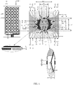
- FIG. 1 is a schematic structural diagram of a touch panel according to an embodiment of the present disclosure.
- the touch panel includes: a base substrate 01, and a first conductive layer 02, an insulation layer 03, and a second conductive layer 04 that are arranged sequentially along a direction away from the base substrate 01.
- the first conductive layer 02 includes: a first touch electrode 021, a second touch electrode 022, a third touch electrode 023, a fourth touch electrode 024, a first connection electrode 025, and a second connection electrode 026.
- the first connection electrode 025 is in an annular shape, and surrounds the second connection electrode 026.
- the first touch electrode 021 and the second touch electrode 022 are disposed on both sides of the first connection electrode 025 in a first direction x
- the third touch electrode 023 and the fourth touch electrode 024 are disposed on both sides of the first connection electrode 025 in a second direction y.
- An included angle between the first direction x and the second direction y is greater than zero.
- the angle between the first direction x and the second direction y is 90 degrees in FIG. 1 .
- the angle between the first direction x and the second direction y may be other degrees greater than zero, for example, 80 degrees.
- the insulation layer 03 includes: two first insulation pads 031, two second insulation pads 032, two third insulation pads 033, and two fourth insulation pads 034.
- One end of each of the two first insulation pads 031 is overlapped onto the first touch electrode 021, and the other end of each of the two first insulation pads is overlapped onto the first connection electrode 025.
- One end of each of the two second insulation pads 032 is overlapped onto the second touch electrode 022, and the other end of each of two second insulation pads is overlapped onto the first connection electrode 025.
- One end of each of the two third insulation pads 033 is overlapped onto the third touch electrode 023, and the other end of each of the two third insulation pads spans the first connection electrode 025 and is overlapped onto the second connection electrode 026.
- One end of each of the two fourth insulation pads 034 is overlapped onto the fourth touch electrode 024, and the other end of each of the two fourth insulation pads spans the first connection electrode 025 and is overlapped onto the second connection electrode 026.
- the second conductive layer 04 includes: two first conductive bridges 041, two second conductive bridges 042, two third conductive bridges 043, and two fourth conductive bridges 044.
- the two first conductive bridges 041 one-to-one correspond to the two first insulation pads 031, each of the first conductive bridges 041 is disposed on the corresponding first insulation pad 031, and both ends of each of the first conductive bridges 041 are electrically connected to the first touch electrode 021 and the first connection electrode 025 respectively.
- the two second conductive bridges 042 one-to-one correspond to the two second insulation pads 032, each of the second conductive bridges 042 is disposed on the corresponding second insulation pad 032, and both ends of each of the second conductive bridges 042 are electrically connected to the second touch electrode 022 and the first connection electrode 025 respectively.
- the two third conductive bridges 043 one-to-one correspond to the two third insulation pads 033, each of the third conductive bridges 042 is disposed on the corresponding third insulation pad 033, and both ends of each of the third conductive bridges 043 are electrically connected to the third touch electrode 023 and the second connection electrode 026 respectively.
- the two fourth conductive bridges 044 one-to-one correspond to the two fourth insulation pads 034, each of the fourth conductive bridges 044 is disposed on the corresponding fourth insulation pad 034, and both ends of each of the fourth conductive bridges 044 are electrically connected to the fourth touch electrode 024 and the second connection electrode 026 respectively.
- the first touch electrode 021, the first connection electrode 025, and the second touch electrode 022 are electrically connected in sequence to form an electrode extending along the first direction x.
- the third touch electrode 023, the second connection electrode 026, and the fourth touch electrode 024 are electrically connected in sequence to form an electrode extending along the second direction y.
- the electrode extending along the first direction x and the electrode extending along the second direction y intersect with each other.
- the touch panel may be a mutual-capacitance touch panel.
- the embodiment of the present disclosure provides a brand-new touch panel.
- the touch panel has a different structure from a touch panel in the related art. Therefore, the structure of the touch panel is enriched.
- an orthographic projection of the first connection electrode 025 on the base substrate 01 is in the shape of an octagonal ring.
- the orthographic projection of the second connection electrode 026 on the base substrate 01 is in the shape of an octagon, and eight inner edges B1 in the octagonal ring are parallel to eight edges B2 of the octagon in one-to-one correspondence. In FIG. 1 , only one inner edge and one edge of the octagon are marked.
- a ring width w of the first connection electrode 025 in the first direction x is greater than a ring width c of the first connection electrode 025 in the second direction y.
- a maximum length L1 of the first connection electrode 025 in the first direction x is greater than a maximum length L2 of the first connection electrode 025 in the second direction y.
- a maximum length L3 of the second connection electrode 026 in the first direction x is less than a maximum length L4 of the second connection electrode 026 in the second direction y.
- the above octagon has a first symmetry axis D1 and a second symmetry axis D2.
- the first symmetry axis D1 is parallel to the first direction x
- the second symmetry axis D2 is parallel to the second direction y.
- the two first conductive bridges 041 are symmetrical about the first symmetry axis D1
- the two second conductive bridges 042 are symmetrical with respect to the first symmetry axis D1
- the two first conductive bridges 041 and the two second conductive bridges 042 are symmetrical with respect to the second symmetry axis D2.
- the two third conductive bridges 043 are symmetrical with respect to the second symmetry axis D2
- the two fourth conductive bridges 044 are symmetrical with respect to the second symmetry axis D2
- the two third conductive bridges 043 and the two fourth conductive bridges 044 are symmetrical with respect to the first symmetry axis D1.
- the conductive bridges in the touch panel are symmetrically distributed, and the distribution of the conductive bridges is relatively uniform, thereby reducing the visibility of the conductive bridges.
- the two first conductive bridges 041 and the two second conductive bridges 042 are all in a striped shape, and perpendicular to an outer edge B3 of the respectively connected octagonal ring, and four outer edges B3 that are perpendicular to the two first conductive bridges 041 and the two second conductive bridges 042 respectively are different (only one outer edge B3 is marked in FIG. 1 ).
- a length of the first conductive bridge 041 is greater than a length of the first insulation pad 031 in the length direction of the first conductive bridge 041, and a length of the first insulation pad 031 in the length direction of the first conductive bridge 041 is greater than a width of a gap between the first conductive bridge 041 and the first connection electrode 025.
- a length of the second conductive bridge 042 is greater than a length of the second insulation pad 032 in the length direction of the second conductive bridge 042, and a length of the second insulation pad 032 in the length direction of the second conductive bridge 042 is greater than a width of a gap between the second conductive bridge 042 and the first connection electrode 025.
- the two third conductive bridges 043 and the two fourth conductive bridges 044 are all in a fold line shape, and each of the two third conductive bridges 043 and the two fourth conductive bridges 044 includes two conductive strips 051.
- a length of the conductive strip 051 is e, an angle between the two conductive strips 051 is ⁇ , 2 d + c 2 sin ⁇ 2 ⁇ e ⁇ 100 um , and 2 tan ⁇ 1 2 d + c ⁇ ⁇ ⁇ ⁇ ⁇ .
- a distance between the first connection electrode 025 and the second connection electrode 026 is d
- a distance between the first connection electrode 025 and the third touch electrode 023 is d
- a distance between the first connection electrode 025 and the fourth touch electrode 024 is d
- a minimum ring width of the first connection electrode 025 is c
- a length of the third insulation pad 033 in a corresponding third direction is f
- a length of the fourth insulation pad 034 in a corresponding fourth direction is f.
- the third direction corresponding to the third insulation pad 033 is perpendicular to a direction of the third touch electrode 023 overlapped by the third insulation pad 033 toward the second connection electrode 025, and the fourth direction corresponding to the fourth insulation pad 034 is perpendicular to a direction of the fourth touch electrode 024 overlapped by the fourth insulation pad 34 toward the second connection electrode 025.
- opening directions of bending angles (for example, the bending angle m and bending angle n in FIG. 1 ) of the two third conductive bridges 043 are opposite. Opening directions of the bending angles (for example, the bending angle p and bending angle ⁇ in FIG. 1 ) of the two fourth conductive bridges 043 are opposite.
- the conductive bridges in the touch panel are not all regularly arranged in the same direction, thereby reducing the visibility of the conductive bridges.
- third conductive bridges 043 and the fourth conductive bridges 044 are all in the fold line shape in FIG. 1 .
- the third conductive bridges 043 and the fourth conductive bridges 044 may also be in a striped shape.
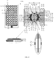
- FIG. 2 is a schematic structural diagram of another touch panel according to an embodiment of the present disclosure.
- the two first conductive bridges 041, the two second conductive bridges 042, the two third conductive bridges 043, and the two fourth conductive bridges 044 are all in a striped shape, and perpendicular to an outer edge B3 of the respectively connected octagonal ring (the first connection electrode 25).
- Eight outer edges B3 that are perpendicular to the two first conductive bridges 041, the two second conductive bridges 042, the two third conductive bridges 043 and the two fourth conductive bridges 044 respectively are different.
- Lengths of the two third conductive bridges 043 and the two fourth conductive bridges 044 are all greater than 2d+c.
- the distance between the first connection electrode and the second connection electrode is d
- the distance between the first connection electrode and the third touch electrode is d
- the distance between the first connection electrode and the fourth touch electrodes is d
- the minimum ring width of the first connection electrode is c.
- the length of the first conductive bridge 041 is greater than the length of the first insulation pad 031 in the length direction of the first conductive bridge, and the length of the first insulation pad 031 in the length direction of the first conductive bridge is greater than the length of the gap between the first conductive bridge 041 and the first connection electrode 025.
- the length of the second conductive bridge 042 is greater than the length of the second insulation pad 032 in the length direction of the second conductive bridge, and the length of the second insulation pad 032 in the length direction of the second conductive bridge is greater than the width of the gap between the second conductive bridge 042 and the first connection electrode 025.
- a distance L1 between the two ends of each of these conductive bridges is less than 220 microns, and a width L2 of each conductive bridge is less than 20 microns. It should be noted that in FIG. 3 , only the strip-shaped conductive bridge is used as an example.
- the distance between the two ends of the conductive bridge is less than 220 microns, and the width of the conductive bridge is less than 20 microns.
- the distance between the two ends of the conductive bridge is greater than 220 microns, and the width of the conductive bridge is greater than 20 microns.
- a smaller distance between the two ends of the conductive bridge indicates a lower visibility of the conductive bridge a smaller width of the conductive bridge and a lower visibility of the conductive bridge. Therefore, in the embodiment of the present disclosure, the visibility of the conductive bridge can be reduced by reducing at least one of the distance between the two ends of at least part of the conductive bridge and the width of the conductive bridge, thereby reducing the shadow of the conductive bridge.
- the distance between the two ends of each conductive bridge is less than 110 microns, 100 microns, or the like.
- the distance between the two ends of the conductive bridge is less than 110 microns or less than 100 microns
- the distance between the two ends of the conductive bridge is further reduced, thereby further reducing the visibility of the conductive bridge.
- the width of each conductive bridge is less than 15 microns, 10 microns, or the like.
- the width L2 of the conductive bridge is less than 10 microns or 15 microns, the width of the conductive bridge is further reduced, thereby further reducing the visibility of the conductive bridge.
- a materials of each of the two first conductive bridges 041, the two second conductive bridges 042, the two third conductive bridges 043, and the two fourth conductive bridges 044 includes metal.
- the conductive bridge 03 in the embodiment of the present disclosure may be light-shielding or transparent.
- the material of the conductive bridge 03 may be metal or other light-shielding conductive materials (for example graphene).
- the material of the conductive bridge 03 may be indium tin oxide or other transparent conductive materials (for example, indium zinc oxide).
- the material of the conductive bridge 03 is metal, since the impedance of the metal is smaller, the conductive effect of the conductive bridge 03 is better.
- the first conductive layer 02 further includes auxiliary electrodes 027 disposed between each two adjacent electrodes of the first touch electrode 021, the second touch electrode 022, the third touch electrode 023, and the four touch electrode 024.
- a gap J is defined between any two electrodes of the auxiliary electrodes 027, the first touch electrode 021, the second touch electrode 022, the third touch electrode 023, and the fourth touch electrode 024.
- auxiliary electrodes 027 are disposed between each two adjacent electrodes of the first touch electrode 021, the second touch electrode 022, the third touch electrode 023, and the fourth touch electrode 024.
- the auxiliary electrode 027 is in a trapezoidal shape, and a side of the lower bottom of each of the two auxiliary electrodes 027 faces the other auxiliary electrode 027.
- the trapezoidal height of the auxiliary electrode 027 may be less than 30 microns. It can be seen that the trapezoidal height is smaller. Therefore, the visibility of the auxiliary electrode 027 can be reduced.
- the touch panel shown in FIG. 1 and FIG. 2 may include a plurality of touch electrodes arranged in an array. These touch electrodes include the first touch electrode, the second touch electrode, the third touch electrode, and the fourth touch electrode.
- the touch panel may further include a plurality of first connection lines 071 corresponding to multiple rows of touch electrodes in one-to-one correspondence, and a plurality of second connection lines 072 corresponding to multiple columns of touch electrodes in one-to-one correspondence.
- One touch electrode in each row of touch electrodes is electrically connected to the first connection line 071 corresponding to the row of touch electrodes
- one touch electrode in each column of touch electrodes is electrically connected to the second connection line 072 corresponding to the column of touch electrodes.
- first connection lines and the second connection lines electrical signals can be applied to the touch electrodes connected to the connection lines, and the electrical signals on the touch electrodes can be collected to detect the touch position.
- a driving electrical signal may be applied to multiple columns of touch electrodes by the plurality of second connection lines in sequence. Every time the driving electrical signal is applied to one column of touch electrodes, the induced electrical signals on multiple rows of touch electrodes are collected by the plurality of first connection lines. After the driving electrical signal is applied to the p th column of touch electrodes, the induced electrical signals collected from the q th row of touch electrodes are not preset electrical signals.
- the intersection position of the p th column of touch electrodes and the q th row of touch electrodes is the touch position, in which p is equal or greater than land q is equal or greater than 1.
- the embodiment of the present disclosure provides a brand-new touch panel.
- the touch panel has a different structure from the touch panel in the related art. Therefore, the structure of the touch panel is enriched.
- the distance between the two ends of the conductive bridge is less than 220 microns, and the width of the conductive bridge is less than 20 microns.
- the distance between the two ends of the conductive bridge is greater than 220 microns, and the width of the conductive bridge is greater than 20 microns.
- a smaller distance between the two ends of the conductive bridge indicates a lower visibility of the conductive bridge, a smaller width of the conductive bridge and a lower visibility of the conductive bridge. Therefore, in the embodiment of the present disclosure, the visibility of the conductive bridge can be reduced by reducing the distance between the two ends of the conductive bridge and the width of the conductive bridge, thereby reducing the shadow of the conductive bridge.
- the embodiment of the present disclosure also provides a touch display panel.
- the touch display panel may include a display panel, and any touch panel according to the embodiment of the present disclosure (for example, the touch panel shown in FIG. 1 or FIG. 2 ).
- the touch panel may be disposed on a light emitting side of the display panel; or, the base substrate in the touch panel is an encapsulation layer in the display panel.
- the above touch display panel may be any product or component having a touch display function, such as a mobile phone, a tablet computer, a television, a display, a notebook computer, a digital photo frame, and a navigator.
- a touch display function such as a mobile phone, a tablet computer, a television, a display, a notebook computer, a digital photo frame, and a navigator.
Landscapes
- Engineering & Computer Science (AREA)
- General Engineering & Computer Science (AREA)
- Theoretical Computer Science (AREA)
- Human Computer Interaction (AREA)
- Physics & Mathematics (AREA)
- General Physics & Mathematics (AREA)
- Quality & Reliability (AREA)
- Position Input By Displaying (AREA)
Abstract
Description
- The present disclosure relates to the technical field of touch, and more particularly, relates to a touch panel and a touch display panel.
- With the development of touch technology, touch panels are increasingly applied to electronic products such as touch screen mobile phones or tablet computers.
- As known by inventor, the touch panel generally includes a base substrate, and a plurality of touch electrodes and a plurality of conductive bridges on the base substrate. The plurality of touch electrodes in the touch panel are arranged in multiple rows and columns, and in either of row direction or column direction of the touch electrodes, adjacent touch electrodes are electrically connected by the conductive bridges.
- Embodiments of the present disclosure provide a touch panel and a touch display panel. The technical solutions are as follows:
- In a first aspect, a touch panel is provided. The touch panel includes: a base substrate, and a first conductive layer, an insulation layer, and a second conductive layer that are sequentially arranged along a direction away from the base substrate; wherein
- the first conductive layer includes: a first touch electrode, a second touch electrode, a third touch electrode, a fourth touch electrode, a first connection electrode, and a second connection electrode; the first connection electrode is in an annular shape, and surrounds the second connection electrode, the first touch electrode, and the second touch electrode are disposed on both sides of the first connection electrode in a first direction, the third touch electrode and the fourth touch electrode are disposed on both sides of the first connection electrode in a second direction, and an included angle between the first direction and the second direction being greater than zero;
- the insulation layer includes: two first insulation pads, two second insulation pads, two third insulation pads, and two fourth insulation pads; wherein one end of each of the two first insulation pads is overlapped onto the first touch electrode, and the other end of each of the two first insulation pads is overlapped onto the first connection electrode; one end of each of the two second insulation pads is overlapped onto the second touch electrode, and the other end of each of the two second insulation pads is overlapped onto the first connection electrode; one end of each of the two third insulation pads is overlapped onto the third touch electrode, and the other end of each of the two third insulation pads spans the first connection electrode and is overlapped onto the second connection electrode; one end of each of the two fourth insulation pads is overlapped onto the fourth touch electrode, and the other end of each of the two fourth insulation pads spans the first connection electrode and is overlapped onto the second connection electrode;
- the second conductive layer includes: two first conductive bridges, two second conductive bridges, two third conductive bridges, and two fourth conductive bridges; wherein the two first conductive bridges one-to-one correspond to the two first insulation pads, each of the first conductive bridges is disposed on the corresponding first insulation pad, and both ends of each of the first conductive bridges are electrically connected to the first touch electrode and the first connection electrode respectively; the two second conductive bridges one-to-one correspond to the two second insulation pads, each of the second conductive bridges is disposed on the corresponding second insulation pad, and both ends of each of the second conductive bridges are electrically connected to the second touch electrode and the first connection electrode respectively; the two third conductive bridges one-to-one correspond to the two third insulation pads, each of the third conductive bridges is disposed on the corresponding third insulation pad, and both ends of each of the third conductive bridges are electrically connected to the third touch electrode and the second connection electrode respectively; and the two fourth conductive bridges one-to-one correspond to the two fourth insulation pads, each of the fourth conductive bridges is disposed on the corresponding fourth insulation pad, and both ends of each of the fourth conductive bridges are electrically connected to the fourth touch electrode and the second connection electrode respectively.
- Optionally, an orthographic projection of the first connection electrode on the base substrate is in the shape of an octagonal ring; an orthographic projection of the second connection electrode on the base substrate is in the shape of an octagon, and eight inner edges in the octagonal ring are parallel to eight edges of the octagon in one-to-one correspondence.
- Optionally, a ring width of the first connection electrode in the first direction is greater than a ring width of the first connection electrode in the second direction;
- a maximum length of the first connection electrode in the first direction is greater than a maximum length of the first connection electrode in the second direction; and
- a maximum length of the second connection electrode in the first direction is less than a maximum length of the second connection electrode in the second direction.
- Optionally, the octagon has a first symmetry axis and a second symmetry axis, the first symmetry axis being parallel to the first direction, and the second symmetry axis being parallel to the second direction;
- the two first conductive bridges are symmetrical with respect to the first symmetry axis, the two second conductive bridges are symmetrical with respect to the first symmetry axis, and the two first conductive bridges and the two second conductive bridges are symmetrical with respect to the second symmetry axis; and
- the two third conductive bridges are symmetrical with respect to the second symmetry axis, the two fourth conductive bridges are symmetrical with respect to the second symmetry axis, and the two third conductive bridges and the two fourth conductive bridges are symmetrical with respect to the first symmetry axis.
- Optionally, the two first conductive bridges and the two second conductive bridges are all in a striped shape and perpendicular to an outer edge of the respectively connected octagonal ring, and four outer edges that are perpendicular to the two first conductive bridges and the two second conductive bridges respectively are different;
- the two third conductive bridges and the two fourth conductive bridges are both in a fold line shape, and each of the two third conductive bridges and the two fourth conductive bridges includes two conductive strips; a length of the conductive strip is e, an angle between the two conductive strips is θ,

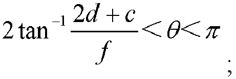
- wherein a distance between the first connection electrode and the second connection electrode is d, a distance between the first connection electrode and the third touch electrode is d, a distance between the first connection electrode and the fourth touch electrode is d, a minimum ring width of the first connection electrode is c, a length of the third insulation pad in a corresponding third direction is f, and a length of the fourth insulation pad in a corresponding fourth direction is f; the third direction corresponding to the third insulation pad is perpendicular to a direction of the third touch electrode overlapped by the third insulation pad toward the second connection electrode, and the fourth direction corresponding to the fourth insulation pad is perpendicular to a direction of the fourth touch electrode overlapped by the fourth insulation pad toward the second connection electrode.
- Optionally, opening directions of bending angles of the two third conductive bridges are opposite, and opening directions of the bending angles of the two fourth conductive bridges are opposite.
- Optionally, the two first conductive bridges, the two second conductive bridges, the two third conductive bridges, and the two fourth conductive bridges are all in a striped shape, and perpendicular to an outer edge of the respectively connected octagonal ring, and eight outer edges that are perpendicular to the two first conductive bridges, the two second conductive bridges, the two third conductive bridges, and the two fourth conductive bridges respectively are different;
- lengths of the two third conductive bridges and the two fourth conductive bridges are all greater than 2d+c;
- wherein a distance between the first connection electrode and the second connection electrode is d, a distance between the first connection electrode and the third touch electrode is d, a distance between the first connection electrode and the fourth touch electrodes is d, a the minimum ring width of the first connection electrode is c.
- Optionally, for the two first conductive bridges, the two second conductive bridges, the two third conductive bridges and the two fourth conductive bridges, a distance between the two ends of each conductive bridge is less than 220 microns, and a width of each conductive bridge is less than 20 microns.
- Optionally, the distance between the two ends of each conductive bridge is less than 110 microns.
- Optionally, the width of each conductive bridge is less than 15 microns.
- Optionally, the first conductive layer further includes: auxiliary electrodes disposed between each two adjacent electrodes of the first touch electrode, the second touch electrode, the third touch electrode and the fourth touch electrode; and
a gap is defined between any two electrodes of the auxiliary electrodes, the first touch electrode, the second touch electrode, the third touch electrode, and the fourth touch electrode. - Optionally, two auxiliary electrodes are disposed between each two adjacent electrodes; and
the auxiliary electrode is in a trapezoidal shape, and a side of the lower bottom of each of the two auxiliary electrodes faces the other auxiliary electrode. - Optionally, a material of each of the two first conductive bridges, the two second conductive bridges, the two third conductive bridges, and the two fourth conductive bridges includes metal.
- In a second aspect, a touch display panel is provided. The touch display panel includes a display panel, and the touch panel as defined in the first aspect; wherein a base substrate in the touch panel is an encapsulation layer in the display panel.
- In a third aspect, a touch display panel is provided. The touch display panel includes a display panel, and the touch panel as defined in the first aspect; wherein the touch panel is disposed on a light emitting side of the display panel.
-
-
FIG. 1 is a schematic structural diagram of a touch panel according to an embodiment of the present disclosure. -
FIG. 2 is a schematic structural diagram of another touch panel according to an embodiment of the present disclosure. -
FIG. 3 is a schematic structural diagram of a conductive bridge according to an embodiment of the present disclosure. - For clearer descriptions of the principles, technical solutions and advantages in the present disclosure, the present disclosure is described in detail below in combination with the accompanying drawings.
-
FIG. 1 is a schematic structural diagram of a touch panel according to an embodiment of the present disclosure. As shown inFIG. 1 , the touch panel includes: abase substrate 01, and a firstconductive layer 02, aninsulation layer 03, and a secondconductive layer 04 that are arranged sequentially along a direction away from thebase substrate 01. - The first
conductive layer 02 includes: a first touch electrode 021, a second touch electrode 022, athird touch electrode 023, afourth touch electrode 024, afirst connection electrode 025, and asecond connection electrode 026. Thefirst connection electrode 025 is in an annular shape, and surrounds thesecond connection electrode 026. The first touch electrode 021 and the second touch electrode 022 are disposed on both sides of thefirst connection electrode 025 in a first direction x, and thethird touch electrode 023 and thefourth touch electrode 024 are disposed on both sides of thefirst connection electrode 025 in a second direction y. An included angle between the first direction x and the second direction y is greater than zero. For example, the angle between the first direction x and the second direction y is 90 degrees inFIG. 1 . Of course, the angle between the first direction x and the second direction y may be other degrees greater than zero, for example, 80 degrees. - The
insulation layer 03 includes: two first insulation pads 031, twosecond insulation pads 032, twothird insulation pads 033, and twofourth insulation pads 034. One end of each of the two first insulation pads 031 is overlapped onto the first touch electrode 021, and the other end of each of the two first insulation pads is overlapped onto thefirst connection electrode 025. One end of each of the twosecond insulation pads 032 is overlapped onto the second touch electrode 022, and the other end of each of two second insulation pads is overlapped onto thefirst connection electrode 025. One end of each of the twothird insulation pads 033 is overlapped onto thethird touch electrode 023, and the other end of each of the two third insulation pads spans thefirst connection electrode 025 and is overlapped onto thesecond connection electrode 026. One end of each of the twofourth insulation pads 034 is overlapped onto thefourth touch electrode 024, and the other end of each of the two fourth insulation pads spans thefirst connection electrode 025 and is overlapped onto thesecond connection electrode 026. - The second
conductive layer 04 includes: two first conductive bridges 041, two secondconductive bridges 042, two thirdconductive bridges 043, and two fourthconductive bridges 044. The two first conductive bridges 041 one-to-one correspond to the two first insulation pads 031, each of the first conductive bridges 041 is disposed on the corresponding first insulation pad 031, and both ends of each of the first conductive bridges 041 are electrically connected to the first touch electrode 021 and thefirst connection electrode 025 respectively. The two secondconductive bridges 042 one-to-one correspond to the twosecond insulation pads 032, each of the secondconductive bridges 042 is disposed on the correspondingsecond insulation pad 032, and both ends of each of the secondconductive bridges 042 are electrically connected to the second touch electrode 022 and thefirst connection electrode 025 respectively. The two thirdconductive bridges 043 one-to-one correspond to the twothird insulation pads 033, each of the thirdconductive bridges 042 is disposed on the correspondingthird insulation pad 033, and both ends of each of the thirdconductive bridges 043 are electrically connected to thethird touch electrode 023 and thesecond connection electrode 026 respectively. The two fourthconductive bridges 044 one-to-one correspond to the twofourth insulation pads 034, each of the fourthconductive bridges 044 is disposed on the correspondingfourth insulation pad 034, and both ends of each of the fourthconductive bridges 044 are electrically connected to thefourth touch electrode 024 and thesecond connection electrode 026 respectively. - As shown in
FIG. 1 , in the embodiment of the present disclosure, the first touch electrode 021, thefirst connection electrode 025, and the second touch electrode 022 are electrically connected in sequence to form an electrode extending along the first direction x. Thethird touch electrode 023, thesecond connection electrode 026, and thefourth touch electrode 024 are electrically connected in sequence to form an electrode extending along the second direction y. Besides, the electrode extending along the first direction x and the electrode extending along the second direction y intersect with each other. The touch panel may be a mutual-capacitance touch panel. - In summary, the embodiment of the present disclosure provides a brand-new touch panel. The touch panel has a different structure from a touch panel in the related art. Therefore, the structure of the touch panel is enriched.
- Optionally, with continued reference to
FIG. 1 , an orthographic projection of thefirst connection electrode 025 on thebase substrate 01 is in the shape of an octagonal ring. The orthographic projection of thesecond connection electrode 026 on thebase substrate 01 is in the shape of an octagon, and eight inner edges B1 in the octagonal ring are parallel to eight edges B2 of the octagon in one-to-one correspondence. InFIG. 1 , only one inner edge and one edge of the octagon are marked. - Optionally, a ring width w of the
first connection electrode 025 in the first direction x is greater than a ring width c of thefirst connection electrode 025 in the second direction y. A maximum length L1 of thefirst connection electrode 025 in the first direction x is greater than a maximum length L2 of thefirst connection electrode 025 in the second direction y. A maximum length L3 of thesecond connection electrode 026 in the first direction x is less than a maximum length L4 of thesecond connection electrode 026 in the second direction y. - Optionally, the above octagon has a first symmetry axis D1 and a second symmetry axis D2. The first symmetry axis D1 is parallel to the first direction x, and the second symmetry axis D2 is parallel to the second direction y. The two first conductive bridges 041 are symmetrical about the first symmetry axis D1, the two second
conductive bridges 042 are symmetrical with respect to the first symmetry axis D1, and the two first conductive bridges 041 and the two secondconductive bridges 042 are symmetrical with respect to the second symmetry axis D2. The two thirdconductive bridges 043 are symmetrical with respect to the second symmetry axis D2, the two fourthconductive bridges 044 are symmetrical with respect to the second symmetry axis D2, and the two thirdconductive bridges 043 and the two fourthconductive bridges 044 are symmetrical with respect to the first symmetry axis D1. In this way, the conductive bridges in the touch panel are symmetrically distributed, and the distribution of the conductive bridges is relatively uniform, thereby reducing the visibility of the conductive bridges. - Optionally, the two first conductive bridges 041 and the two second
conductive bridges 042 are all in a striped shape, and perpendicular to an outer edge B3 of the respectively connected octagonal ring, and four outer edges B3 that are perpendicular to the two first conductive bridges 041 and the two secondconductive bridges 042 respectively are different (only one outer edge B3 is marked inFIG. 1 ). Optionally, a length of the first conductive bridge 041 is greater than a length of the first insulation pad 031 in the length direction of the first conductive bridge 041, and a length of the first insulation pad 031 in the length direction of the first conductive bridge 041 is greater than a width of a gap between the first conductive bridge 041 and thefirst connection electrode 025. Similarly, a length of the secondconductive bridge 042 is greater than a length of thesecond insulation pad 032 in the length direction of the secondconductive bridge 042, and a length of thesecond insulation pad 032 in the length direction of the secondconductive bridge 042 is greater than a width of a gap between the secondconductive bridge 042 and thefirst connection electrode 025. - The two third
conductive bridges 043 and the two fourthconductive bridges 044 are all in a fold line shape, and each of the two thirdconductive bridges 043 and the two fourthconductive bridges 044 includes twoconductive strips 051. A length of theconductive strip 051 is e, an angle between the twoconductive strips 051 is θ,

first connection electrode 025 and thesecond connection electrode 026 is d, a distance between thefirst connection electrode 025 and thethird touch electrode 023 is d, a distance between thefirst connection electrode 025 and thefourth touch electrode 024 is d, a minimum ring width of thefirst connection electrode 025 is c, a length of thethird insulation pad 033 in a corresponding third direction is f, and a length of thefourth insulation pad 034 in a corresponding fourth direction is f. The third direction corresponding to thethird insulation pad 033 is perpendicular to a direction of thethird touch electrode 023 overlapped by thethird insulation pad 033 toward thesecond connection electrode 025, and the fourth direction corresponding to thefourth insulation pad 034 is perpendicular to a direction of thefourth touch electrode 024 overlapped by the fourth insulation pad 34 toward thesecond connection electrode 025. - Optionally, with continued reference to
FIG. 1 , opening directions of bending angles (for example, the bending angle m and bending angle n inFIG. 1 ) of the two thirdconductive bridges 043 are opposite. Opening directions of the bending angles (for example, the bending angle p and bending angle θ inFIG. 1 ) of the two fourthconductive bridges 043 are opposite. In this way, the conductive bridges in the touch panel are not all regularly arranged in the same direction, thereby reducing the visibility of the conductive bridges. - It should be noted that the third
conductive bridges 043 and the fourthconductive bridges 044 are all in the fold line shape inFIG. 1 . Optionally, the thirdconductive bridges 043 and the fourthconductive bridges 044 may also be in a striped shape. - Illustratively,
FIG. 2 is a schematic structural diagram of another touch panel according to an embodiment of the present disclosure. As shown inFIG. 2 , the two first conductive bridges 041, the two secondconductive bridges 042, the two thirdconductive bridges 043, and the two fourthconductive bridges 044 are all in a striped shape, and perpendicular to an outer edge B3 of the respectively connected octagonal ring (the first connection electrode 25). Eight outer edges B3 that are perpendicular to the two first conductive bridges 041, the two secondconductive bridges 042, the two thirdconductive bridges 043 and the two fourthconductive bridges 044 respectively are different. Lengths of the two thirdconductive bridges 043 and the two fourthconductive bridges 044 are all greater than 2d+c. The distance between the first connection electrode and the second connection electrode is d, the distance between the first connection electrode and the third touch electrode is d, the distance between the first connection electrode and the fourth touch electrodes is d, and the minimum ring width of the first connection electrode is c. - Optionally, the length of the first conductive bridge 041 is greater than the length of the first insulation pad 031 in the length direction of the first conductive bridge, and the length of the first insulation pad 031 in the length direction of the first conductive bridge is greater than the length of the gap between the first conductive bridge 041 and the
first connection electrode 025. Similarly, the length of the secondconductive bridge 042 is greater than the length of thesecond insulation pad 032 in the length direction of the second conductive bridge, and the length of thesecond insulation pad 032 in the length direction of the second conductive bridge is greater than the width of the gap between the secondconductive bridge 042 and thefirst connection electrode 025. - In addition, regardless of the shapes of the two first conductive bridges, two second conductive bridges, two third conductive bridges, and two fourth conductive bridges (for example, the shape shown in
FIG. 1 orFIG. 2 ), as shown inFIG. 3 , a distance L1 between the two ends of each of these conductive bridges is less than 220 microns, and a width L2 of each conductive bridge is less than 20 microns. It should be noted that inFIG. 3 , only the strip-shaped conductive bridge is used as an example. - In the touch panel according to the embodiment of the present disclosure, the distance between the two ends of the conductive bridge is less than 220 microns, and the width of the conductive bridge is less than 20 microns. However, in the related art, the distance between the two ends of the conductive bridge is greater than 220 microns, and the width of the conductive bridge is greater than 20 microns. A smaller distance between the two ends of the conductive bridge indicates a lower visibility of the conductive bridge a smaller width of the conductive bridge and a lower visibility of the conductive bridge. Therefore, in the embodiment of the present disclosure, the visibility of the conductive bridge can be reduced by reducing at least one of the distance between the two ends of at least part of the conductive bridge and the width of the conductive bridge, thereby reducing the shadow of the conductive bridge.
- Optionally, the distance between the two ends of each conductive bridge is less than 110 microns, 100 microns, or the like. When the distance between the two ends of the conductive bridge is less than 110 microns or less than 100 microns, the distance between the two ends of the conductive bridge is further reduced, thereby further reducing the visibility of the conductive bridge. Optionally, the width of each conductive bridge is less than 15 microns, 10 microns, or the like. When the width L2 of the conductive bridge is less than 10 microns or 15 microns, the width of the conductive bridge is further reduced, thereby further reducing the visibility of the conductive bridge.
- Optionally, a materials of each of the two first conductive bridges 041, the two second
conductive bridges 042, the two thirdconductive bridges 043, and the two fourthconductive bridges 044 includes metal. It should be noted that theconductive bridge 03 in the embodiment of the present disclosure may be light-shielding or transparent. When theconductive bridge 03 is light-shielding, the material of theconductive bridge 03 may be metal or other light-shielding conductive materials (for example graphene). When theconductive bridge 03 is transparent, the material of theconductive bridge 03 may be indium tin oxide or other transparent conductive materials (for example, indium zinc oxide). In addition, when the material of theconductive bridge 03 is metal, since the impedance of the metal is smaller, the conductive effect of theconductive bridge 03 is better. - With continued reference to
FIG. 1 orFIG. 2 , regardless of the shape of the conductive bridge, the firstconductive layer 02 further includesauxiliary electrodes 027 disposed between each two adjacent electrodes of the first touch electrode 021, the second touch electrode 022, thethird touch electrode 023, and the fourtouch electrode 024. In addition, a gap J is defined between any two electrodes of theauxiliary electrodes 027, the first touch electrode 021, the second touch electrode 022, thethird touch electrode 023, and thefourth touch electrode 024. - Optionally, two
auxiliary electrodes 027 are disposed between each two adjacent electrodes of the first touch electrode 021, the second touch electrode 022, thethird touch electrode 023, and thefourth touch electrode 024. Besides, theauxiliary electrode 027 is in a trapezoidal shape, and a side of the lower bottom of each of the twoauxiliary electrodes 027 faces the otherauxiliary electrode 027. - Optionally, the trapezoidal height of the
auxiliary electrode 027 may be less than 30 microns. It can be seen that the trapezoidal height is smaller. Therefore, the visibility of theauxiliary electrode 027 can be reduced. - In addition, the touch panel shown in
FIG. 1 andFIG. 2 may include a plurality of touch electrodes arranged in an array. These touch electrodes include the first touch electrode, the second touch electrode, the third touch electrode, and the fourth touch electrode. The touch panel may further include a plurality offirst connection lines 071 corresponding to multiple rows of touch electrodes in one-to-one correspondence, and a plurality ofsecond connection lines 072 corresponding to multiple columns of touch electrodes in one-to-one correspondence. One touch electrode in each row of touch electrodes is electrically connected to thefirst connection line 071 corresponding to the row of touch electrodes, and one touch electrode in each column of touch electrodes is electrically connected to thesecond connection line 072 corresponding to the column of touch electrodes. - By the first connection lines and the second connection lines, electrical signals can be applied to the touch electrodes connected to the connection lines, and the electrical signals on the touch electrodes can be collected to detect the touch position. Exemplarily, during detection of the touch position, a driving electrical signal may be applied to multiple columns of touch electrodes by the plurality of second connection lines in sequence. Every time the driving electrical signal is applied to one column of touch electrodes, the induced electrical signals on multiple rows of touch electrodes are collected by the plurality of first connection lines. After the driving electrical signal is applied to the pth column of touch electrodes, the induced electrical signals collected from the qth row of touch electrodes are not preset electrical signals. When the induced electrical signals collected from other rows of touch electrodes are all preset electrical signals, it can be determined that the intersection position of the pth column of touch electrodes and the qth row of touch electrodes is the touch position, in which p is equal or greater than land q is equal or greater than 1.
- In summary, the embodiment of the present disclosure provides a brand-new touch panel. The touch panel has a different structure from the touch panel in the related art. Therefore, the structure of the touch panel is enriched.
- Moreover, in the touch panel according to the embodiment of the present disclosure, the distance between the two ends of the conductive bridge is less than 220 microns, and the width of the conductive bridge is less than 20 microns. However, in the related art, the distance between the two ends of the conductive bridge is greater than 220 microns, and the width of the conductive bridge is greater than 20 microns. A smaller distance between the two ends of the conductive bridge indicates a lower visibility of the conductive bridge, a smaller width of the conductive bridge and a lower visibility of the conductive bridge. Therefore, in the embodiment of the present disclosure, the visibility of the conductive bridge can be reduced by reducing the distance between the two ends of the conductive bridge and the width of the conductive bridge, thereby reducing the shadow of the conductive bridge.
- The embodiment of the present disclosure also provides a touch display panel. The touch display panel may include a display panel, and any touch panel according to the embodiment of the present disclosure (for example, the touch panel shown in
FIG. 1 orFIG. 2 ). Exemplarily, the touch panel may be disposed on a light emitting side of the display panel; or, the base substrate in the touch panel is an encapsulation layer in the display panel. - Further, the above touch display panel may be any product or component having a touch display function, such as a mobile phone, a tablet computer, a television, a display, a notebook computer, a digital photo frame, and a navigator.
- It should be noted that in the accompanying drawings, for clarity of the illustration, the dimension of the layers and areas may be scaled up. It may be understood that when an element or layer is described as being "above" another element or layer, the described element or layer may be directly on the other element or layer, or at least one intermediate layer may be arranged between the described element or layer and the other element or layer. In addition, It may be understood that when an element or layer is described as being "below" another element or layer, the described element or layer may be directly below the other element or layer, or at least one intermediate layer may be arranged between the described element or layer and the other element or layer. In addition, it may be further understood that when a layer or element is described as being arranged "between" two layers or elements, the described layer or element may be the only layer between the two layers or elements, or at least one intermediate layer or element may be arranged between the described element or layer and the two layers or elements. In the whole specification described above, like reference numerals denote like elements.
- In the present disclosure, the terms such as "first", "second", "third", and "fourth" are merely for a descriptive purpose, and cannot be understood as indicating or implying a relative importance. The term "a plurality of" means two or more in number, unless otherwise defined.
- The foregoing descriptions are merely optional embodiments of the present disclosure, and are not intended to limit the present disclosure. Within the spirit and principles of the disclosure, any modifications, equivalent substitutions, improvements, or the like are within the protection scope of the present disclosure.
Claims (15)
- A touch panel, comprising: a base substrate, a first conductive layer, an insulation layer, and a second conductive layer that are sequentially arranged along a direction away from the base substrate; whereinthe first conductive layer comprises: a first touch electrode, a second touch electrode , a third touch electrode, a fourth touch electrode, a first connection electrode, and a second connection electrode; wherein the first connection electrode is in an annular shape and surrounds the second connection electrode, the first touch electrode and the second touch electrode are disposed on both sides of the first connection electrode in a first direction, and the third touch electrode and the fourth touch electrode are disposed on both sides of the first connection electrode in a second direction, an included angle between the first direction and the second direction being greater than zero;the insulation layer comprises: two first insulation pads, two second insulation pads, two third insulation pads, and two fourth insulation pads; wherein one end of each of the two first insulation pads is overlapped onto the first touch electrode, and the other end of each of the two first insulation pads is overlapped onto the first connection electrode; one end of each of the two second insulation pads is overlapped onto the second touch electrode, and the other end of each of the two second insulation pads is overlapped onto the first connection electrode; one end of each of the two third insulation pads is overlapped onto the third touch electrode, and the other end of each of the two third insulation pads spans the first connection electrode and is overlapped onto the second connection electrode; one end of each of the two fourth insulation pads is overlapped onto the fourth touch electrode, and the other end of each of the two fourth insulation pads spans the first connection electrode and is overlapped onto the second connection electrode;the second conductive layer comprises: two first conductive bridges, two second conductive bridges, two third conductive bridges, and two fourth conductive bridges; wherein the two first conductive bridges one-to-one correspond to the two first insulation pads, each of the first conductive bridges is disposed on the corresponding first insulation pad, and both ends of each of the first conductive bridges are electrically connected to the first touch electrode and the first connection electrode respectively; the two second conductive bridges one-to-one correspond to the two second insulation pads, each of the second conductive bridges is disposed on the corresponding second insulation pad, and both ends of each of the second conductive bridges are electrically connected to the second touch electrode and the first connection electrode respectively; the two third conductive bridges one-to-one correspond to the two third insulation pads, each of the third conductive bridges is disposed on the corresponding third insulation pad, and both ends of each of the third conductive bridges are electrically connected to the third touch electrode and the second connection electrode respectively; and the two fourth conductive bridges one-to-one correspond to the two fourth insulation pads, each of the fourth conductive bridges is disposed on the corresponding fourth insulation pad, and both ends of each of the fourth conductive bridges are electrically connected to the fourth touch electrode and the second connection electrode respectively.
- The touch panel according to claim 1, wherein an orthographic projection of the first connection electrode on the base substrate is in the shape of an octagonal ring; an orthographic projection of the second connection electrode on the base substrate is in the shape of an octagon, and eight inner edges in the octagonal ring are parallel to eight edges of the octagon in one-to-one correspondence.
- The touch panel according to claim 2, whereina ring width of the first connection electrode in the first direction is greater than a ring width of the first connection electrode in the second direction;a maximum length of the first connection electrode in the first direction is greater than a maximum length of the first connection electrode in the second direction; anda maximum length of the second connection electrode in the first direction is less than a maximum length of the second connection electrode in the second direction.
- The touch panel according to claim 2 or 3, wherein the octagon has a first symmetry axis and a second symmetry axis, the first symmetry axis being parallel to the first direction, and the second symmetry axis being parallel to the second direction; whereinthe two first conductive bridges are symmetrical with respect to the first symmetry axis, the two second conductive bridges are symmetrical with respect to the first symmetry axis, and the two first conductive bridges and the two second conductive bridges are symmetrical with respect to the second symmetry axis; andthe two third conductive bridges are symmetrical with respect to the second symmetry axis, the two fourth conductive bridges are symmetrical with respect to the second symmetry axis, and the two third conductive bridges and the two fourth conductive bridges are symmetrical with respect to the first symmetry axis.
- The touch panel according to any one of claims 2 to 4, wherein the two first conductive bridges and the two second conductive bridges are all in a striped shape and perpendicular to an outer edge of the respectively connected octagonal ring, and four outer edges that are perpendicular to the two first conductive bridges and the two second conductive bridges respectively are different;the two third conductive bridges and the two fourth conductive bridges are all in a fold line shape, and each of the two third conductive bridges and the two fourth conductive bridges comprises two conductive strips; a length of the conductive strip is e, an included angle between the two conductive strips is θ,

 wherein a distance between the first connection electrode and the second connection electrode is d, a distance between the first connection electrode and the third touch electrode is d, a distance between the first connection electrode and the fourth touch electrode is d, a minimum ring width of the first connection electrode is c, a length of the third insulation pad in a corresponding third direction is f, and a length of the fourth insulation pad in a corresponding fourth direction is f; the third direction corresponding to the third insulation pad is perpendicular to a direction of the third touch electrode overlapped by the third insulation pad toward the second connection electrode, and the fourth direction corresponding to the fourth insulation pad is perpendicular to a direction of the fourth touch electrode overlapped by the fourth insulation pad toward the second connection electrode.
 - The touch panel according to claim 5, wherein opening directions of bending angles of the two third conductive bridges are opposite, and opening directions of the bending angles of the two fourth conductive bridges are opposite.
- The touch panel according to any one of claims 2 to 4, wherein the two first conductive bridges, the two second conductive bridges, the two third conductive bridges, and the two fourth conductive bridges are all in a striped shape, and perpendicular to an outer edge of the respectively connected octagonal ring, and eight outer edges that are perpendicular to the two first conductive bridges, the two second conductive bridges, the two third conductive bridges, and the two fourth conductive bridges respectively are different;lengths of the two third conductive bridges and the two fourth conductive bridges are all greater than 2d+c;wherein a distance between the first connection electrode and the second connection electrode is d, a distance between the first connection electrode and the third touch electrode is d, a distance between the first connection electrode and the fourth touch electrodes is d, and a minimum ring width of the first connection electrode is c.
- The touch panel according to any one of claims 1 to 7, wherein for the two first conductive bridges, the two second conductive bridges, the two third conductive bridges and the two fourth conductive bridges, a distance between two ends of each conductive bridge is less than 220 microns, and a width of each conductive bridge is less than 20 microns.
- The touch panel according to claim 8, wherein the distance between the two ends of each conductive bridge is less than 110 microns.
- The touch panel according to claim 8 or 9, wherein the width of each conductive bridge is less than 15 microns.
- The touch panel according to any one of claims 1 to 10, wherein the first conductive layer further comprises: auxiliary electrodes disposed between each two adjacent electrodes of the first touch electrode, the second touch electrode, the third touch electrode, and the fourth touch electrode; and
a gap is defined between any two electrodes of the auxiliary electrodes, the first touch electrode, the second touch electrode, the third touch electrode, and the fourth touch electrode. - The touch panel according to claim 11, wherein two auxiliary electrodes are disposed between each two adjacent electrodes; and
the auxiliary electrode is in a trapezoidal shape, and a side of the lower bottom of each of the two auxiliary electrodes faces the other auxiliary electrode. - The touch panel according to any one of claims 1 to 12, wherein a material of each of the two first conductive bridges, the two second conductive bridges, the two third conductive bridges, and the two fourth conductive bridges comprises a metal.
- A touch display panel, comprising a display panel, and the touch panel as defined in any one of claims 1 to 13; wherein a base substrate in the touch panel is an encapsulation layer in the display panel.
- A touch display panel, comprising a display panel, and the touch panel as defined in any one of claims 1 to 13; wherein the touch panel is disposed on a light emitting side of the display panel.
Applications Claiming Priority (1)
| Application Number | Priority Date | Filing Date | Title |
|---|---|---|---|
| PCT/CN2019/098680 WO2021016935A1 (en) | 2019-07-31 | 2019-07-31 | Touch control panel and touch control display panel |
Publications (4)
| Publication Number | Publication Date |
|---|---|
| EP4006701A1 true EP4006701A1 (en) | 2022-06-01 |
| EP4006701A4 EP4006701A4 (en) | 2022-08-03 |
| EP4006701B1 EP4006701B1 (en) | 2025-11-19 |
| EP4006701C0 EP4006701C0 (en) | 2025-11-19 |
Family
ID=74228235
Family Applications (1)
| Application Number | Title | Priority Date | Filing Date |
|---|---|---|---|
| EP19932222.3A Active EP4006701B1 (en) | 2019-07-31 | 2019-07-31 | Touch control panel and touch control display panel |
Country Status (4)
| Country | Link |
|---|---|
| US (2) | US11269472B2 (en) |
| EP (1) | EP4006701B1 (en) |
| CN (1) | CN112673337B (en) |
| WO (1) | WO2021016935A1 (en) |
Families Citing this family (5)
| Publication number | Priority date | Publication date | Assignee | Title |
|---|---|---|---|---|
| CN205068345U (en) * | 2015-10-29 | 2016-03-02 | 合肥鑫晟光电科技有限公司 | Touch -control structure, touch screen and display device |
| US11269472B2 (en) * | 2019-07-31 | 2022-03-08 | Chengdu Boe Optoelectronics Technology Co., Ltd. | Touch panel and touch display panel |
| CN112650411B (en) * | 2020-12-28 | 2024-04-19 | 武汉天马微电子有限公司 | Display panel, preparation method of display panel and display device |
| KR20240115963A (en) * | 2023-01-19 | 2024-07-26 | 삼성디스플레이 주식회사 | Electronic device |
| US12197687B1 (en) * | 2023-12-22 | 2025-01-14 | Samsung Display Co., Ltd. | Electronic device |
Family Cites Families (16)
| Publication number | Priority date | Publication date | Assignee | Title |
|---|---|---|---|---|
| TW200842681A (en) | 2007-04-27 | 2008-11-01 | Tpk Touch Solutions Inc | Touch pattern structure of a capacitive touch panel |
| JP2010271796A (en) | 2009-05-19 | 2010-12-02 | Optrex Corp | Connection structure between electrodes and touch panel |
| KR102341436B1 (en) * | 2014-08-06 | 2021-12-23 | 삼성디스플레이 주식회사 | Fabrication method of touch screen panel and touch screen panel |
| KR101721299B1 (en) | 2014-12-30 | 2017-03-30 | 엘지디스플레이 주식회사 | Touch sensing system comprising touch screen panel |
| CN104932764B (en) | 2015-06-25 | 2017-12-08 | 京东方科技集团股份有限公司 | A kind of capacitance type touch control screen and preparation method thereof, display device |
| US10162441B2 (en) * | 2016-03-10 | 2018-12-25 | Raydium Semiconductor Corporation | Capacitive touch panel |
| KR102670409B1 (en) * | 2016-10-31 | 2024-05-30 | 엘지디스플레이 주식회사 | Liquid crystal display device |
| CN108628483B (en) * | 2017-03-15 | 2021-03-05 | 京东方科技集团股份有限公司 | Touch unit, mutual capacitance touch screen and touch display device |
| JP2018190331A (en) * | 2017-05-11 | 2018-11-29 | 株式会社ジャパンディスプレイ | Touch sensor and display device having touch sensor |
| CN107357475B (en) * | 2017-06-27 | 2020-12-29 | 上海天马微电子有限公司 | Touch panel and display device |
| CN107704120A (en) * | 2017-08-30 | 2018-02-16 | 京东方科技集团股份有限公司 | Flexible touch screen and its manufacture method, flexible display apparatus |
| CN107908319B (en) * | 2018-01-03 | 2021-08-06 | 京东方科技集团股份有限公司 | Touch substrate and display device |
| CN108693994A (en) * | 2018-03-29 | 2018-10-23 | 武汉华星光电半导体显示技术有限公司 | Touch-control structure, OLED show touch panel and touch control display device |
| CN109634457A (en) * | 2018-12-03 | 2019-04-16 | 武汉华星光电半导体显示技术有限公司 | Touch control electrode and touch control display apparatus |
| CN109976578B (en) * | 2019-03-22 | 2020-09-22 | 合肥鑫晟光电科技有限公司 | Touch substrate, manufacturing method thereof and touch display device |
| US11269472B2 (en) * | 2019-07-31 | 2022-03-08 | Chengdu Boe Optoelectronics Technology Co., Ltd. | Touch panel and touch display panel |
-
2019
- 2019-07-31 US US16/958,964 patent/US11269472B2/en active Active
- 2019-07-31 WO PCT/CN2019/098680 patent/WO2021016935A1/en not_active Ceased
- 2019-07-31 EP EP19932222.3A patent/EP4006701B1/en active Active
- 2019-07-31 CN CN201980001204.8A patent/CN112673337B/en active Active
-
2022
- 2022-01-27 US US17/585,962 patent/US11644935B2/en active Active
Also Published As
| Publication number | Publication date |
|---|---|
| US20210405824A1 (en) | 2021-12-30 |
| US11269472B2 (en) | 2022-03-08 |
| US20220147194A1 (en) | 2022-05-12 |
| WO2021016935A1 (en) | 2021-02-04 |
| EP4006701B1 (en) | 2025-11-19 |
| CN112673337B (en) | 2023-05-12 |
| EP4006701A4 (en) | 2022-08-03 |
| CN112673337A (en) | 2021-04-16 |
| EP4006701C0 (en) | 2025-11-19 |
| US11644935B2 (en) | 2023-05-09 |
Similar Documents
| Publication | Publication Date | Title |
|---|---|---|
| US11644935B2 (en) | Touch panel having second conductive layer and touch display panel | |
| US10684716B2 (en) | Stretchable panel and flexible display device | |
| US10928952B2 (en) | Touch display panel and touch display device | |
| EP2717137B1 (en) | Touch screen panel | |
| US9081458B2 (en) | In-cell touch display device | |
| US8570285B2 (en) | Touch display panel and touch sensing unit thereof | |
| US20190235668A1 (en) | Touch screen and mobile terminal | |
| JP6313471B2 (en) | Display device with position input function | |
| US10296138B2 (en) | Array substrate, display panel, method for determining touch center coordinates and display device | |
| US9869894B2 (en) | Embedded touch display panel and touch display device | |
| WO2014021168A1 (en) | Touch panel substrate and display device | |
| US10139967B2 (en) | Touch screen and display device | |
| KR20150109338A (en) | Touch panel and display device | |
| JP6494287B2 (en) | Touch screen, touch panel, display device, and electronic device | |
| CN104508613A (en) | Touch panel substrate and display device | |
| US20150220176A1 (en) | Touch panel substrate and display device | |
| US20170177124A1 (en) | Display apparatus with touch detection function | |
| US11221716B2 (en) | Touch substrate and touch display apparatus with touch electrodes having zigzag boundaries | |
| US11226694B2 (en) | Touch display substrate, touch display method and touch display device | |
| WO2014077315A1 (en) | Touch panel substrate, electronic device, and production method for electronic device | |
| US11042254B2 (en) | Touch display devices | |
| US20180004341A1 (en) | Touch display apparatus | |
| US9401712B2 (en) | Touch panel substrate with first grid electrodes and second grid electrodes | |
| US11500502B2 (en) | Touch-controlling base plate and displaying device |
Legal Events
| Date | Code | Title | Description |
|---|---|---|---|
| STAA | Information on the status of an ep patent application or granted ep patent |
Free format text: STATUS: UNKNOWN |
|
| STAA | Information on the status of an ep patent application or granted ep patent |
Free format text: STATUS: THE INTERNATIONAL PUBLICATION HAS BEEN MADE |
|
| PUAI | Public reference made under article 153(3) epc to a published international application that has entered the european phase |
Free format text: ORIGINAL CODE: 0009012 |
|
| STAA | Information on the status of an ep patent application or granted ep patent |
Free format text: STATUS: REQUEST FOR EXAMINATION WAS MADE |
|
| 17P | Request for examination filed |
Effective date: 20201214 |
|
| AK | Designated contracting states |
Kind code of ref document: A1 Designated state(s): AL AT BE BG CH CY CZ DE DK EE ES FI FR GB GR HR HU IE IS IT LI LT LU LV MC MK MT NL NO PL PT RO RS SE SI SK SM TR |
|
| A4 | Supplementary search report drawn up and despatched |
Effective date: 20220701 |
|
| RIC1 | Information provided on ipc code assigned before grant |
Ipc: H01L 27/32 20060101ALI20220627BHEP Ipc: G06F 3/044 20060101ALI20220627BHEP Ipc: G06F 3/041 20060101AFI20220627BHEP |
|
| DAV | Request for validation of the european patent (deleted) | ||
| DAX | Request for extension of the european patent (deleted) | ||
| STAA | Information on the status of an ep patent application or granted ep patent |
Free format text: STATUS: EXAMINATION IS IN PROGRESS |
|
| 17Q | First examination report despatched |
Effective date: 20231124 |
|
| RIC1 | Information provided on ipc code assigned before grant |
Ipc: G06F 3/044 20060101ALI20250522BHEP Ipc: G06F 3/041 20060101AFI20250522BHEP |
|
| GRAP | Despatch of communication of intention to grant a patent |
Free format text: ORIGINAL CODE: EPIDOSNIGR1 |
|
| STAA | Information on the status of an ep patent application or granted ep patent |
Free format text: STATUS: GRANT OF PATENT IS INTENDED |
|
| INTG | Intention to grant announced |
Effective date: 20250702 |
|
| GRAS | Grant fee paid |
Free format text: ORIGINAL CODE: EPIDOSNIGR3 |
|
| GRAA | (expected) grant |
Free format text: ORIGINAL CODE: 0009210 |
|
| STAA | Information on the status of an ep patent application or granted ep patent |
Free format text: STATUS: THE PATENT HAS BEEN GRANTED |
|
| AK | Designated contracting states |
Kind code of ref document: B1 Designated state(s): AL AT BE BG CH CY CZ DE DK EE ES FI FR GB GR HR HU IE IS IT LI LT LU LV MC MK MT NL NO PL PT RO RS SE SI SK SM TR |
|
| REG | Reference to a national code |
Ref country code: CH Ref legal event code: F10 Free format text: ST27 STATUS EVENT CODE: U-0-0-F10-F00 (AS PROVIDED BY THE NATIONAL OFFICE) Effective date: 20251119 Ref country code: GB Ref legal event code: FG4D |
|
| REG | Reference to a national code |
Ref country code: DE Ref legal event code: R096 Ref document number: 602019078389 Country of ref document: DE |
|
| REG | Reference to a national code |
Ref country code: IE Ref legal event code: FG4D |
|
| U01 | Request for unitary effect filed |
Effective date: 20251218 |
|
| U07 | Unitary effect registered |
Designated state(s): AT BE BG DE DK EE FI FR IT LT LU LV MT NL PT RO SE SI Effective date: 20260102 |
|
| PG25 | Lapsed in a contracting state [announced via postgrant information from national office to epo] |
Ref country code: ES Free format text: LAPSE BECAUSE OF FAILURE TO SUBMIT A TRANSLATION OF THE DESCRIPTION OR TO PAY THE FEE WITHIN THE PRESCRIBED TIME-LIMIT Effective date: 20251119 |
|
| PG25 | Lapsed in a contracting state [announced via postgrant information from national office to epo] |
Ref country code: NO Free format text: LAPSE BECAUSE OF FAILURE TO SUBMIT A TRANSLATION OF THE DESCRIPTION OR TO PAY THE FEE WITHIN THE PRESCRIBED TIME-LIMIT Effective date: 20260219 |
|
| PG25 | Lapsed in a contracting state [announced via postgrant information from national office to epo] |
Ref country code: HR Free format text: LAPSE BECAUSE OF FAILURE TO SUBMIT A TRANSLATION OF THE DESCRIPTION OR TO PAY THE FEE WITHIN THE PRESCRIBED TIME-LIMIT Effective date: 20251119 |
|
| PG25 | Lapsed in a contracting state [announced via postgrant information from national office to epo] |
Ref country code: RS Free format text: LAPSE BECAUSE OF FAILURE TO SUBMIT A TRANSLATION OF THE DESCRIPTION OR TO PAY THE FEE WITHIN THE PRESCRIBED TIME-LIMIT Effective date: 20260219 |
|
| PG25 | Lapsed in a contracting state [announced via postgrant information from national office to epo] |
Ref country code: IS Free format text: LAPSE BECAUSE OF FAILURE TO SUBMIT A TRANSLATION OF THE DESCRIPTION OR TO PAY THE FEE WITHIN THE PRESCRIBED TIME-LIMIT Effective date: 20260319 |
|
| PG25 | Lapsed in a contracting state [announced via postgrant information from national office to epo] |
Ref country code: PL Free format text: LAPSE BECAUSE OF FAILURE TO SUBMIT A TRANSLATION OF THE DESCRIPTION OR TO PAY THE FEE WITHIN THE PRESCRIBED TIME-LIMIT Effective date: 20251119 |
|
| PG25 | Lapsed in a contracting state [announced via postgrant information from national office to epo] |
Ref country code: SM Free format text: LAPSE BECAUSE OF FAILURE TO SUBMIT A TRANSLATION OF THE DESCRIPTION OR TO PAY THE FEE WITHIN THE PRESCRIBED TIME-LIMIT Effective date: 20251119 |
|
| PG25 | Lapsed in a contracting state [announced via postgrant information from national office to epo] |
Ref country code: CZ Free format text: LAPSE BECAUSE OF FAILURE TO SUBMIT A TRANSLATION OF THE DESCRIPTION OR TO PAY THE FEE WITHIN THE PRESCRIBED TIME-LIMIT Effective date: 20251119 |
|
| PG25 | Lapsed in a contracting state [announced via postgrant information from national office to epo] |
Ref country code: SK Free format text: LAPSE BECAUSE OF FAILURE TO SUBMIT A TRANSLATION OF THE DESCRIPTION OR TO PAY THE FEE WITHIN THE PRESCRIBED TIME-LIMIT Effective date: 20251119 |