EP4006690A1 - Optischer rechnerchip, system und datenverarbeitungstechnologie - Google Patents
Optischer rechnerchip, system und datenverarbeitungstechnologie Download PDFInfo
- Publication number
- EP4006690A1 EP4006690A1 EP20844087.5A EP20844087A EP4006690A1 EP 4006690 A1 EP4006690 A1 EP 4006690A1 EP 20844087 A EP20844087 A EP 20844087A EP 4006690 A1 EP4006690 A1 EP 4006690A1
- Authority
- EP
- European Patent Office
- Prior art keywords
- optical signal
- array
- data
- concave mirror
- modulator
- Prior art date
- Legal status (The legal status is an assumption and is not a legal conclusion. Google has not performed a legal analysis and makes no representation as to the accuracy of the status listed.)
- Pending
Links
Images
Classifications
-
- G—PHYSICS
- G06—COMPUTING OR CALCULATING; COUNTING
- G06E—OPTICAL COMPUTING DEVICES
- G06E3/00—Devices not provided for in group G06E1/00, e.g. for processing analogue or hybrid data
- G06E3/001—Analogue devices in which mathematical operations are carried out with the aid of optical or electro-optical elements
-
- G—PHYSICS
- G06—COMPUTING OR CALCULATING; COUNTING
- G06N—COMPUTING ARRANGEMENTS BASED ON SPECIFIC COMPUTATIONAL MODELS
- G06N3/00—Computing arrangements based on biological models
- G06N3/02—Neural networks
- G06N3/06—Physical realisation, i.e. hardware implementation of neural networks, neurons or parts of neurons
- G06N3/067—Physical realisation, i.e. hardware implementation of neural networks, neurons or parts of neurons using optical means
- G06N3/0675—Physical realisation, i.e. hardware implementation of neural networks, neurons or parts of neurons using optical means using electro-optical, acousto-optical or opto-electronic means
-
- G—PHYSICS
- G06—COMPUTING OR CALCULATING; COUNTING
- G06E—OPTICAL COMPUTING DEVICES
- G06E3/00—Devices not provided for in group G06E1/00, e.g. for processing analogue or hybrid data
- G06E3/001—Analogue devices in which mathematical operations are carried out with the aid of optical or electro-optical elements
- G06E3/005—Analogue devices in which mathematical operations are carried out with the aid of optical or electro-optical elements using electro-optical or opto-electronic means
-
- G—PHYSICS
- G06—COMPUTING OR CALCULATING; COUNTING
- G06N—COMPUTING ARRANGEMENTS BASED ON SPECIFIC COMPUTATIONAL MODELS
- G06N3/00—Computing arrangements based on biological models
- G06N3/02—Neural networks
- G06N3/04—Architecture, e.g. interconnection topology
- G06N3/045—Combinations of networks
-
- G—PHYSICS
- G06—COMPUTING OR CALCULATING; COUNTING
- G06N—COMPUTING ARRANGEMENTS BASED ON SPECIFIC COMPUTATIONAL MODELS
- G06N3/00—Computing arrangements based on biological models
- G06N3/02—Neural networks
- G06N3/04—Architecture, e.g. interconnection topology
- G06N3/0464—Convolutional networks [CNN, ConvNet]
Definitions
- This application relates to the field of computer technologies, and in particular, to an optical computing chip and system, and a data processing technology.
- Deep learning is a neural network constructed to mimic a human brain, and can achieve a better recognition effect than conventional shallow learning. Because a deep learning algorithm is complex and has a huge amount of computation, but a conventional central processing unit is inefficient in processing large-scale computation, research on hardware used for AI acceleration has gradually become a hot research topic.
- Analog optical computing is a type of optical computing.
- Analog optical computing is an operation of using physical characteristics of optical components to complete a corresponding mathematical process.
- analog optical computing is mainly based on a classical 4F system, and two modulators are used to process input data in spatial frequency domain based on a Fourier transform effect of a lens to complete corresponding computation.
- a convex lens used in an existing 4F system is a three-dimensional component, and therefore cannot be integrated on a chip.
- an additional computing device needs to be used to first compute spectrum data of data based on Fourier transform, and then modulate the spectrum data on a modulator.
- An implementation process is relatively complex.
- This application provides an optical computing chip and system, and a data processing technology, to implement optical computing on a chip and improve data computing efficiency.
- an embodiment of the present invention provides an optical computing chip, including a first concave mirror, a light source array, and a modulator array.
- the light source array is located on an objective focal plane of the first concave mirror
- the modulator array is located on an image focal plane of the first concave mirror.
- the light source array is configured to generate a first optical signal based on first data.
- the first concave mirror is configured to output a first reflected optical signal based on the first optical signal.
- the modulator array is configured to: receive the first reflected optical signal, obtain first spectrum plane distribution data based on the first reflected optical signal, and modulate the first spectrum plane distribution data onto the modulator array.
- the optical computing chip in this embodiment of the present invention uses a concave mirror, and the concave mirror is a one-dimensional component, it is easier to fabricate and integrate the concave mirror on the chip. Therefore, it is possible to implement optical computing on the chip.
- a modulator in the optical computing chip can generate a photocurrent based on intensity of incident light, the first spectrum plane distribution data of the first reflected optical signal can be obtained, the spectrum plane distribution data can be directly obtained in a process of implementing optical computing, and the obtained spectrum plane distribution data is modulated onto the modulator array. In this manner, no additional computing device needs to be used to assist in obtaining spectrum plane distribution data. Further, computation efficiency is improved in the optical computation process, and the implementation is simple and efficient.
- the light source array is further configured to generate a second optical signal based on second data.
- the first concave mirror is further configured to output a second reflected optical signal based on the second optical signal.
- the modulator array is further configured to obtain a third optical signal based on the second reflected optical signal and the first spectrum plane distribution data.
- the optical computing chip further includes a second concave mirror and a detector array.
- the modulator array is further located on an objective focal plane of the second concave mirror.
- the detector array is located on an image focal plane of the second concave mirror.
- the second concave mirror is configured to receive the third optical signal, and output a third reflected optical signal based on the third optical signal.
- the detector array is configured to detect the third reflected optical signal, where distribution of the third reflected optical signal on the detector array is used to indicate a convolution result of the first data and the second data.
- the modulator array used can directly obtain optical spectrum plane distribution data based on the reflected optical signal, and can modulate the first data onto the modulator array, in a process of implementing convolution computation of the first data and the second data, no additional computing device is required to assist in obtaining spectrum plane distribution data of the first data. Therefore, computation efficiency can be improved.
- the modulator array includes a plurality of modulators, and a transmittance of each modulator for the first reflected optical signal is used to indicate a value in the first spectrum plane distribution data.
- the modulator is implemented by at least one of the following components: a doped silicon waveguide, an electroabsorption modulator, and a semiconductor optical amplifier SOA.
- the light source array includes a plurality of light emitting elements, and each light emitting element is configured to generate incoherent light. Because light emitted by the light source array used in this embodiment of the present invention is incoherent light, and a data modulation function can also be considered, an I/O speed of the optical computing chip is greatly improved in comparison with that of an existing spatial optical computing system.
- the light source array and the detector array are located on a same side of the chip.
- a structure of the optical computing chip can be made more compact, and a chip size can be reduced.
- the first concave mirror and the second concave mirror are parabolic concave mirrors.
- the light source array includes a plurality of stacked light source subarrays
- the modulator array includes a plurality of stacked modulator subarrays
- the detector array includes a plurality of stacked detector subarrays.
- convolution computation can be simultaneously implemented on data in a plurality of rows and a plurality of columns.
- this application provides an optical computing system, where the optical computing system includes a processor and the optical computing chip according to the first aspect or any possible implementation of the first aspect.
- the processor is configured to input first data to the optical computing chip.
- the optical computing system further includes a light source array drive circuit and a modulator array drive circuit.
- the light source array drive circuit is connected to the processor and the light source array of the optical computing chip, and configured to apply a first drive signal to the light source array based on the first data.
- the modulator array drive circuit is connected to the modulator array, and the modulator array drive circuit is configured to sample the first spectrum plane distribution data obtained by the optical computing chip, and apply a first modulation signal to the optical computing chip based on the first spectrum plane distribution data.
- the light source array is specifically configured to generate the first optical signal based on the first drive signal.
- the modulator array is specifically configured to modulate the first spectrum plane distribution data onto the modulator array based on the first modulation signal.
- the optical computing system further includes a detector array drive circuit.
- the detector array drive circuit is connected to the detector array of the optical computing chip.
- the detector array drive circuit is configured to capture the third reflected optical signal detected by the detector array, and perform analog-to-digital conversion on the third reflected optical signal to obtain the convolution result of the first data and the second data.
- this application further provides a data processing method performed by the optical computing chip according to the first aspect or any implementation of the first aspect.
- the method after the light source array in the optical computing chip generates a first optical signal based on first data, the first concave mirror in the optical computing chip outputs a first reflected optical signal based on the first optical signal; and the modulator array in the optical computing chip obtains first spectrum plane distribution data based on the first reflected optical signal, and modulates the first spectrum plane distribution data onto the modulator array.
- the light source array may further generate a second optical signal based on second data.
- the modulator array obtains a third optical signal based on the second reflected optical signal and the first spectrum plane distribution data.
- the second concave mirror in the optical computing chip outputs a third reflected optical signal based on the third optical signal.
- the detector array in the optical computing chip may detect the third reflected optical signal, where distribution of the third reflected optical signal on the detector array is used to indicate a convolution result of the first data and the second data.
- this application further provides a computer program product, including program code, where instructions included in the program code are executed by a computer, to implement the data processing method according to the third aspect or any possible implementation of the third aspect.
- this application further provides a computer-readable storage medium, where the computer-readable storage medium is configured to store program code, and instructions included in the program code are executed by a computer, to implement the data processing method according to the third aspect or any possible implementation of the third aspect.
- An artificial neural network (artificial neural network, ANN), referred to as a neural network (neural network, NN) or a neural-like network, is a mathematical model or a computing model that mimics a structure and function of a biological neural network (a central nervous system of an animal, and especially a brain) in the fields of machine learning and cognitive science, and is used to perform estimation or approximation on a function.
- the artificial neural network may include neural networks such as a convolutional neural network (convolutional neural network, CNN), a deep neural network (deep neural network, DNN), and a multilayer perceptron (multilayer perception, MLP).
- An algorithm of a neural network system is complex and an amount of computation is huge. Therefore, a very high requirement is posed on data computation efficiency. To improve computation efficiency, optical computing that uses physical characteristics of optical components to complete a corresponding mathematical operation process is applied.
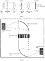
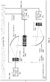
- the following first uses a 4F optical computing system 100 shown in FIG. 1 as an example to briefly describe a process of implementing convolution computation in a neural network system by using the optical computing system.
- the 4F optical computing system may also be referred to as a 4F system.
- the 4F system is a system including two convex lenses, two light modulators, and one detector.
- a first modulator 102 is located at an object focal point of a first convex lens 104.
- a second modulator 106 is located at an image focal point of the first convex lens 104, and is located at an object focal point of a second convex lens 108.
- a spacing between the first convex lens 104 and the second convex lens 108 is a sum of focal lengths of the two convex lenses (104 and 108).
- a detector 110 is located at an image focal point of the second convex lens 108, and a length of the entire system is four times the focal length.
- the data A needs to be modulated onto the first modulator 102, and a Fourier spectrum of the data B needs to be modulated onto the second modulator 106.
- a laser beam emitted by a laser (laser) 101 passes through the first modulator 102
- an optical signal passing through the first modulator 102 is an optical signal generated based on the data A.
- Fourier transform is performed on the optical signal through the first convex lens 104, a spatial frequency domain image is presented on the second modulator 106, so that a multiplication operation between the data A and the convolutional data B previously modulated onto the second modulator 106 is completed.
- Inverse Fourier transform is performed on a signal output by the second modulator 106 through the second convex lens 108.
- the detector 110 detects light intensity of the optical signal output by the second convex lens 108, to obtain a convolution result C of the data A and the data B. It can be learned from the process of implementing convolution computation in the 4F system shown in FIG. 1 that, in the entire convolution computation process, modulation of the data B onto the second modulator 106 needs to consume extra time, and other computation processes do not consume time. Therefore, a computation speed is very high.
- the spatial light modulator is a two-dimensional component, I/O concurrency of the system is high, a quantity of components in the entire system is small, and a result is relatively simple.
- the convex lens used in the 4F system shown in FIG. 1 is a three-dimensional component and cannot be integrated on a two-dimensional plane. Therefore, the 4F system shown in FIG. 1 cannot be integrated on a chip.
- the 4F system shown in FIG. 1 uses a single light source and emits coherent light, two modulators are required in the computation process, so that two pieces of to-be-computed data are modulated onto the two modulators in the computation process respectively.
- the modulator in the existing 4F system cannot generate a photocurrent based on an optical signal, and does not have a function of recording spectrum plane distribution data, two modulators are required in the computation process.
- an additional computing device needs to be used to first compute spectrum data of the data B based on the Fourier transform, and then modulate the spectrum data of the data B onto the second modulator 106.
- An implementation process is relatively complex.
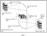
- FIG. 2 is a schematic structural diagram of an optical computing chip according to an embodiment of the present invention.
- FIG. 2 shows an on-chip optical computing system.
- the optical computing chip 200 may include a light source array 202, a modulator array 204, a detector array 206, a first concave mirror 208, and a second concave mirror 210.
- the light source array 202 is located on an objective focal plane of the first concave mirror 208.
- the modulator array 204 is located on an image focal plane of the first concave mirror 208, and the modulator array 204 is also located on an objective focal plane of the second concave mirror 210.
- the detector array 206 is located on an image focal plane of the second concave mirror 210.
- the light source array 202 is configured to modulate and send data, and used as a data input unit of the optical computing chip 200.
- the light source array 202 may generate a plurality of optical signals of different light intensity based on the input data.
- the first concave mirror 208 is configured to implement standard Fourier transform on an optical signal of the data sent by the light source array 202.
- the modulator array 204 has two working modes: a recording mode and a modulation mode. The recording mode is used to obtain an image on a spectrum plane presented after the optical signal of the data sent by the light source array 202 passes through the first concave mirror 208.
- the modulation mode is used to modulate, onto the modulator array 204, the image that is on the spectrum plane and that is of the optical signal of the data sent by the light source array 202.
- the second concave mirror 210 is configured to implement standard inverse Fourier transform on the optical signal that passes through the modulator array 204.
- the detector array 206 is configured to detect a light intensity signal, and is used as a result output unit of the optical computing chip 200. The following describes in detail specific implementation of each component in the optical computing chip 200.
- the light source array 202 may include a plurality of light emitting elements 302, and the plurality of light emitting elements may be arranged along a straight line. Intensity of light emitted by each of the light emitting elements may be modulated. Distribution of luminous intensity of the light source array along a straight line corresponds to data that needs to be input to the optical computing chip. As shown in FIG. 3 , the light source array 202 may include a plurality of light emitting elements 302 arranged along a straight line. The light emitting element 302 is configured to generate incoherent light under the action of a voltage. Intensity of light emitted by the light emitting element 302 may vary with the change of the voltage.
- the light emitted by the light emitting element 302 may be modulated.
- the light source array 202 may be implemented by a semiconductor light emitting diode (LED) array.
- the light emitting element 302 may be an LED.
- Each LED can emit incoherent light with a large divergence angle, and its luminous intensity varies with the change of the injection voltage, so that modulation can be implemented.
- an amplitude of light emitted by the LED may represent to-be-computed data.
- E k x f x k .
- an emission light source may be considered as superposition of a plurality of light sources.
- a light field of light emitted by the LED may be approximately a Gaussian function.
- the light source array 202 may also be implemented by using a laser array.
- the light emitting element 302 may be a laser.
- a lens with a divergence angle may be disposed in front of each laser, so that each laser can emit light with a large divergence angle.
- modulation of the light intensity can also be implemented by adding a material with a variable transmittance in front of the laser. It may be understood that in an actual application, using a laser as a light emitting element may be equivalent to an effect of using an LED as a light emitting element, but an implementation process is relatively complex.
- the light source array 202 in this embodiment of the present invention uses a plurality of light sources and emits incoherent light. Because intensity of each light source in the light source array may be changed, a plurality of optical signals of different light intensity can be emitted based on different values in the data without using an additional modulator, and an optical signal generation speed is higher.
- the modulator array 204 has two working modes: the recording mode and the modulation mode.
- the recording mode is used to obtain the image on the spectrum plane obtained after the optical signal of the data sent by the light source array 202 passes through the first concave mirror 208.
- the modulation mode is used to modulate, onto the modulator array 204, the image that is on the spectrum plane and that is of the optical signal of the data sent by the light source array 202.
- the modulator array 204 may include a plurality of modulators.
- the plurality of modulators may be arranged along a straight line to obtain the modulator array 204.
- each modulator in the modulator array 204 may record and modulate intensity of received incident light.
- the modulator may be implemented by using a structure based on different principles such as a doped silicon waveguide, an electroabsorption modulator, and a semiconductor optical amplifier (semiconductor optical amplifier, SOA).
- a doped silicon waveguide an electroabsorption modulator
- SOA semiconductor optical amplifier
- incident light intensity may be recorded by detecting a magnitude of an incident photocurrent of the SOA.
- intensity of an optical signal passing through the SOA may be changed by changing a light transmittance.
- the SOA may be made of a semiconductor quantum well material. Because the light transmittance of the SOA may vary with different voltages, the light transmittance of the SOA may be changed between 0 and 1 through voltage control. Specifically, in a state in which a voltage passing through the SOA is a reversed bias voltage, a photocurrent is generated in the SOA based on incident light, so that light intensity distribution may be obtained by detecting a magnitude of the photocurrent.
- spectrum distribution data after Fourier transform is performed on an object plane signal of the first concave mirror 208 may be directly obtained by detecting the light intensity distribution on the modulator array in this manner. In this way, the recording function of the modulator is implemented.
- an incident light transmittance of the SOA also changes.
- optical spatial spectrum plane data may also be modulated by using the change of the incident light transmittance of the SOA. For example, different voltages (which may also be referred to as modulation signals) may be input to corresponding modulators based on values in the obtained spatial spectrum plane data, where a light transmittance of one modulator in the modulator array may reflect a value in the spectrum plane data. Therefore, the spectrum plane data can be modulated onto the modulator array in this manner, to implement the modulation function of the modulator array.
- the SOA under the action of a forward voltage may implement the function of recording light intensity
- the SOA under the action of a reversed bias voltage may also implement the function of modulating light intensity.
- a material and an operating voltage of the modulator array 204 are not specifically limited, provided that the modulator array 204 can implement two functions: recording and modulation.
- the modulator array 204 needs to generate a photocurrent after receiving the incident light, so that the light intensity distribution of the incident light is obtained by detecting a magnitude of the photocurrent, to implement recording of the light intensity.
- the modulator array 204 can change the light transmittance according to the change of the applied voltage, to modulate the light intensity.
- the detector array 206 is configured to detect light intensity of the incident light, and used as a result output unit of the optical computing chip 200.
- the detector array 206 may be implemented by using a semiconductor photodiode (photodiode, PD) array, a photoconductive detector array (for example, a photoresistor array), or the like.
- the first concave mirror 208 is configured to implement standard Fourier transform on the optical signal of the data sent by the light source array 202.
- the second concave mirror 210 is configured to implement standard inverse Fourier transform on the optical signal that passes through the modulator array 204.
- Fourier transform is implemented by using a convex lens.
- a concave reflective mirror is used to implement Fourier transform and inverse Fourier transform. The following briefly describes principles of implementing Fourier transform and inverse Fourier transform by a concave mirror.
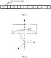
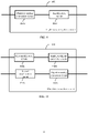
- FIG. 4 is a schematic diagram of an optical path of a spherical reflective concave mirror according to an embodiment of the present invention.
- a phase delay generated after incident light is reflected is basically caused by geometry of the reflective mirror.
- ⁇ z R ⁇ x 2 + y 2 ⁇ x 2 + y 2 2 R .
- the concave reflective mirror can also implement Fourier transform on the incident light, and a corresponding focal length is R/2.
- a parabolic concave reflective mirror may be used to replace the spherical concave reflective mirror.
- a y-axis is an optical axis
- p is a constant related to a parabolic focal point
- Z 0 is coordinates of a parabolic vertex.
- the parabolic concave reflective mirror also has the same function as the convex lens, and can implement Fourier transform on incident light, and a corresponding focal length of the parabolic concave reflective mirror is p/2.
- a size of a parabolic surface of a parabolic concave reflective mirror may be determined based on a ratio of a size of a light source to a size of the concave mirror.
- the present invention is not limited to using a parabolic concave mirror.
- the spherical concave mirror may also be used.
- reflective surfaces of both the first concave mirror 208 and the second concave mirror 210 may form air reflective surfaces by using a deep etching process.
- an end face may also be plated with a highly reflective film.
- Another advantage of forming a reflective surface by etching is that an arbitrary surface can be precisely defined, so that the foregoing parabolic concave mirror can be fabricated to achieve a more accurate Fourier transform effect.
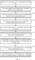
- FIG. 5 is a flowchart of a method for implementing convolution computation of data by using an optical computing chip according to an embodiment of the present invention.
- the following uses an example in which a convolution computation is implemented on first data and second data to describe how the computing chip implements the convolution computation. It may be understood that both the first data and the second data may include a plurality of real numbers.
- the method includes the following steps.
- the light source array 202 generates a first optical signal based on the first data.
- the light emitting elements 302 in the light source array 202 may generate optical signals of different light intensity based on changes of voltages.
- voltages of different magnitudes may be input to different light emitting elements 302 in the light source array 202 based on values in the first data, so that the light emitting elements 302 in the light source array 202 emit incoherent light of different light intensity based on different values, to obtain the first optical signal.
- the first optical signal includes incoherent light emitted by the different light emitting elements 302 in the light source array 202.
- the first concave mirror 208 outputs a first reflected optical signal based on the first optical signal.
- the light source array 202 is located at a focal point on an object plane of the first concave mirror 208, the first concave mirror 208 may receive paraxial light emitted by the light source array 202, and the first reflected optical signal is output after the first optical signal is reflected by the first concave mirror 208.
- the modulator array 204 obtains first spectrum plane distribution data based on the first reflected optical signal.
- the modulator array 204 needs to work in a recording mode.
- the modulators in the modulator array 204 are made of materials that enable the modulators to generate a photocurrent upon receiving incident light. Therefore, after the modulator array 204 receives the first reflected optical signal, the modulator generates a photocurrent based on the received first reflected optical signal without applying a voltage to the modulator array 204.
- the first reflected optical signal can be recorded in an electrical form by detecting photocurrent intensity in the modulator, so that optical spatial spectrum plane distribution data of the first reflected optical signal is obtained.
- the spectrum plane distribution data of the first reflected optical signal may also be referred to as first spectrum plane distribution data.
- the modulator array 204 modulates the first spectrum plane distribution data onto the modulator array.
- the modulator array 204 needs to work in a modulation mode. Specifically, different voltages may be applied to the modulators based on different data recorded by the modulators in the modulator array 204, and the spectrum plane distribution data of the first reflected optical signal obtained in step 506 is modulated as a transmittance of the modulators in the modulator array 204, and the first spectrum plane distribution data is represented on the modulators. It may be understood that different voltages are applied to different data, so that different voltages are applied to different modulators in the modulator array 204.
- the light source array 202 generates a second optical signal based on the second data.
- the light source array 202 may generate the second optical signal based on the second data.
- voltages of different magnitudes may be input to different light emitting elements 302 in the light source array 202 based on values in the second data, so that the light emitting elements 302 in the light source array 202 emit incoherent light of different light intensity based on different values, to obtain the second optical signal.
- the first concave mirror 208 outputs a second reflected optical signal based on the second optical signal.
- the modulator array 204 obtains a third optical signal based on the second reflected optical signal and the recorded first spectrum plane distribution data. As described above, because the first spectrum plane distribution data of the first reflected optical signal obtained based on the first data has been modulated onto the modulator array 204, the first spectrum plane distribution data is represented as the light transmittance of the modulators in the modulator array 204.
- the modulator array 204 When the modulator array 204 receives the second reflected optical signal, after the second reflected optical signal passes through the modulators in the modulator array 204, the third optical signal may be obtained based on the second reflected optical signal together with the first spectrum plane distribution data modulated onto the modulator array 204. In this manner, the modulator array 204 completes an optical spatial spectrum plane multiplication operation on spectrum plane distribution data of the second reflected optical signal and the spectrum plane distribution data of the first reflected optical signal.
- the third optical signal represents an optical signal obtained after the first reflected optical signal and the second reflected optical signal pass through the modulator array 204, and the third optical signal represents a result of a multiplication operation on the first spectrum plane distribution data and the spectrum plane distribution data of the second reflected optical signal in optical spatial frequency domain.
- the spectrum plane distribution data of the second reflected optical signal may also be referred to as second spectrum plane distribution data.
- the second concave mirror 210 outputs a third reflected optical signal based on the third optical signal.
- the first concave mirror 208 and the second concave mirror 210 may perform Fourier transform and inverse Fourier transform. As described above, Fourier transform is performed on both the first data and the second data after the first data and the second data pass through the first concave mirror.
- the second concave mirror 210 after receiving the third optical signal output by the modulator array 204, the second concave mirror 210 outputs the third reflected optical signal, where the third reflected optical signal is a result obtained by performing inverse Fourier transform on a convolution computation result output by the modulator array 204.
- the detector array 206 detects the third reflected optical signal. Distribution of the third reflected optical signal on the detector array is used to indicate a convolution result of the first data and the second data. As described above, the detectors in the detector array 206 may detect intensity of incident light. Therefore, the convolution computation result of the first data and the second data obtained through the inverse Fourier transform may be obtained based on the detected light intensity of the third reflected optical signal.
- FIG. 6 is a schematic structural diagram of another optical computing chip according to an embodiment of the present invention.
- a difference from the on-chip integrated optical computing chip provided in FIG. 2 lies in that, in the optical computing chip shown in FIG. 6 , the light source array 202 and the detector array 206 are disposed on a same side of the chip. Therefore, a structure of the entire computing chip is more compact, and a chip size can be reduced. As shown in FIG. 6 , in comparison with the optical computing chip shown in FIG.
- positions of the first concave mirror 208, the second concave mirror 210, and the modulator array 204 remain unchanged, and positions of the light source array 202, the modulator array 204, and the detector array 206 relative to focal points of the first concave mirror 208 and the second concave mirror 210 also remain unchanged respectively.
- positions of the first concave mirror 208, the second concave mirror 210, and the modulator array 204 remain unchanged, and positions of the light source array 202, the modulator array 204, and the detector array 206 relative to focal points of the first concave mirror 208 and the second concave mirror 210 also remain unchanged respectively.
- each component shown in FIG. 6 refer to descriptions of each component in the optical computing chip shown in FIG. 2 .
- For a process in which the computing chip shown in FIG. 6 implements convolution computation of data refer to descriptions of FIG. 2 and FIG. 5 . Details are not described herein again.
- the optical computing chip provided in this embodiment of the present invention uses a concave mirror, and the concave mirror is a one-dimensional component, it is easy to fabricate and integrate the concave mirror on the chip. Therefore, it is possible to implement optical computing on the chip.
- a modulator in the optical computing chip can generate a photocurrent based on intensity of incident light, the intensity of the received incident light can be recorded and modulated, and data can be directly recorded and modulated onto the modulator array in a process of implementing optical computing. No additional computing device needs to be used to assist in obtaining spectrum plane data. Therefore, computation efficiency is improved, and the implementation is simple and efficient.
- light emitted by the light source array used in this embodiment of the present invention is incoherent light, and a data modulation function can also be considered. Therefore, an I/O speed of the optical computing chip is greatly improved in comparison with that of an existing spatial optical computing system.
- the concave mirror is used to replace a convex lens in a conventional 4F system, it is easier to fabricate and integrate the concave mirror on the chip. Because all components can be integrated on the chip, in comparison with the existing 4F optical computing system, optical computing chip has a smaller size and higher flexibility, and requires lower fabrication costs. Further, in comparison with the existing optical computing system that completes convolution computation only as a multiplier-adder, the on-chip optical computing chip can implement complex optical computing such as Fourier transform, convolution, and autocorrelation.
- the optical computing chips described in FIG. 2 and FIG. 6 are one-dimensional convolution computing systems, and can implement convolution computation of one-dimensional data.
- an embodiment of the present invention provides an optical computing chip that can implement multi-dimensional data computation.
- a plurality of one-layer light source arrays may be stacked to implement a multi-dimensional light source array (for example, a two-dimensional light source array), a plurality of one-dimensional modulator arrays may be stacked to implement a multi-dimensional modulator array, and a plurality of one-dimensional detector arrays may be stacked to implement a multi-dimensional detector array.
- multi-dimensional convolution computation can be implemented by increasing an area of a concave mirror.
- the optical computing chip shown in FIG. 7 may include a light source array 702, a modulator array 704, a detector array 706, a first concave mirror 708, and a second concave mirror 710.
- the light source array 702 may include a plurality of stacked light source subarrays 7022
- the modulator array 704 may include a plurality of stacked modulator subarrays 7042
- the detector array 706 may include a plurality of stacked detector subarrays 7062. Structures and operating principles of the light source subarray 7022, the modulator subarray 7042, and the detector subarray 7062 may be respectively shown in the light source array 202, the modulator array 204, and the detector array 206 in FIG. 2 .
- one light source subarray 7022, one modulator subarray 7042, and one detector subarray 7062 cooperate to process one row of data in first data and one row of data in second data, to implement the function shown in FIG. 2 or FIG. 6 .
- one light source subarray 7022 may be configured to generate a first optical subsignal based on the first row of data in the first data, and generate a second optical subsignal based on the first row of data in the second data.
- One modulator subarray 7042 is configured to record and modulate a reflected optical signal based on the first optical subsignal and the second optical subsignal.
- One detector subarray 7062 is configured to detect a computation result of the first row of data in the first data and the first row of data in the second data. It may be understood that in comparison with the optical computing chip shown in FIG. 2 , because both the light source array 702 and the modulator array 704 are formed by stacking a plurality of subarrays, in the optical computing chip shown in FIG. 7 , thicknesses of the first concave mirror 708 and the second concave mirror 710 are increased relative to thicknesses of the first concave mirror 208 and the second concave mirror 210 in FIG. 2 . Therefore, optical signals emitted by the light source array 702 and the modulator array 704 can be reflected. It may be understood that because the optical computing chip shown in FIG.
- ⁇ 7 may include a plurality of stacked light source subarrays, a plurality of stacked modulator subarrays, and a plurality of stacked detector subarrays, convolution computation of multi-dimensional data (which may also be referred to as multi-row and multi-column data) can be implemented.
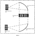
- FIG. 8 is a schematic structural diagram of an optical computing system according to an embodiment of the present invention.
- the optical computing system 800 mainly includes three parts: a control plane 802, an optical computing chip 804, and a peripheral drive circuit.
- the peripheral drive circuit may include a light source array drive circuit 806, a modulator array drive circuit 810, and a detector array drive circuit 808.
- the control plane 802 may include a component that can implement functions such as control and processing, such as a processor.
- control plane 802 may include a processing component such as a central processing unit (central processing unit, CPU), an application-specific integrated circuit (application-specific integrated circuit, ASIC), or a field-programmable gate array (field-programmable gate array, FPGA).
- a processing component such as a central processing unit (central processing unit, CPU), an application-specific integrated circuit (application-specific integrated circuit, ASIC), or a field-programmable gate array (field-programmable gate array, FPGA).
- the optical computing chip 804 may be shown in FIG. 2 , FIG. 6 , or FIG. 7 .
- the optical computing chip 804 may include a light source array 8042, a modulator array 8044, a detector array 8046, a first concave mirror 8048, and a second concave mirror 8049.
- the optical computing chip 804 refer to the description in the foregoing embodiment.
- the light source array 8042, the modulator array 8044, and the detector array 8046 in the optical computing chip 804 are active components, and therefore need to be driven by corresponding external drive circuits. Therefore, the optical computing system 800 may further include peripheral circuits such as the light source array drive circuit 806, the modulator array drive circuit 810, and the detector array drive circuit 808. The following briefly describes the peripheral circuits in the optical computing system with reference to the foregoing process of implementing convolution computation on the first data and the second data.
- the light source array drive circuit 806 is configured to receive to-be-computed data sent by the control plane 802, and convert the received data into a corresponding voltage, to drive the light source array 8042 to emit a corresponding optical signal.
- the light source array drive circuit 806 may receive the first data and the second data that are sent by the control plane 802, and convert the first data and the second data into corresponding voltages.
- the light source array drive circuit 806 may include a digital-to-analog conversion circuit 8062 and an amplification circuit 8064.
- the digital-to-analog conversion circuit 8062 in the light source array drive circuit 806 may perform digital-to-analog conversion on the received first data, and convert the first data into a corresponding voltage. Then the amplification circuit 8064 amplifies the voltage obtained through the conversion, and sends a corresponding amplified voltage to the light source array 8042, to drive the light source array 8042 to convert a received electrical signal into a corresponding optical signal, thereby converting the first data into a first optical signal.
- the modulator array provided in this embodiment of the present invention has two working modes: recording and modulation. Therefore, there is a bidirectional data exchange process between the modulator array 8044 and the modulator array drive circuit 810 in the optical computing chip 804.
- the modulator array drive circuit 810 may include a first amplification circuit 8102, an analog-to-digital conversion circuit 8104, a digital-to-analog conversion circuit 8106, and a second amplification circuit 8108.
- the modulator array 8044 works in the recording mode, after receiving a first reflected optical signal from the first concave mirror 8048, the modulator array 8044 generates a corresponding photocurrent.
- the modulator array drive circuit 810 may capture the photocurrent generated by the modulator array 8044.
- the photocurrent generated by the modulator array 8044 based on the received first reflected optical signal is used to indicate spectrum plane distribution data of the first reflected optical signal.
- the analog-to-digital conversion circuit 8104 converts the amplified photocurrent into data, to obtain the spectrum plane distribution data of the first reflected optical signal. In other words, after converting the received photocurrent into a digital signal, the analog-to-digital conversion circuit 8104 may record the spectrum plane distribution data of the first reflected optical signal.
- the modulator array drive circuit 810 may send the spectrum plane distribution data of the first reflected optical signal to the control plane 802.
- the control plane 802 performs processing such as denoising, normalization, or format conversion on the spectrum plane distribution data of the received first reflected optical signal, and then sends processed data to the modulator array drive circuit 810.
- the digital-to-analog conversion circuit 8106 in the modulator array drive circuit 810 may receive the processed data sent by the control plane 802, and convert the received data into a corresponding analog signal.
- the second amplification circuit 8108 inputs a corresponding voltage (which may also be referred to as a modulation signal) to the modulator array based on the converted analog signal, to drive the modulator array 8044 to work in the modulation mode and modulate corresponding data onto the modulator array 8044.
- a corresponding voltage which may also be referred to as a modulation signal
- the first amplification circuit 8102 and the second amplification circuit 8108 may also be implemented by using one circuit, and the analog-to-digital conversion circuit 8104 and the digital-to-analog conversion circuit 8106 may also be integrated.
- the detector array drive circuit 808 may also include an amplification circuit 8082 and an analog-to-digital conversion circuit 8084.
- the detector array drive circuit 808 is configured to receive a light intensity signal detected by the detector array 8046. It may be understood that the light intensity signal detected by the detector array 8046 is in a form of a photocurrent.
- the amplification circuit 8082 may amplify a received photocurrent signal detected by the detector array 8046.
- the analog-to-digital conversion circuit 8084 in the detector array drive circuit 808 may convert the received analog signal into a digital signal, to obtain a computation result of the first data and the second data, and may send the computation result to the control plane 802.
- a data input of the entire optical computing system 800 may be implemented by driving the light source array 8042 by the control plane 802 by using the light source array drive circuit 806, the computation result of the optical computing chip 804 may be captured by the detector array drive circuit 808, and finally, the captured data is returned to the control plane 802.
- the described apparatus embodiment is merely an example.
- the division into the modules is merely logical function division, and another division manner may be used in actual implementation.
- a plurality of modules or components may be combined or integrated into another system, or some features may be ignored or may not be performed.
- the modules discussed in the foregoing embodiments may be connected to each other in electrical, mechanical, or other forms.
- the modules described as separate components may or may not be physically separate.
- a component displayed as a module may or may not be a physical module.
- functional modules in the embodiments of this application may exist independently, or may be integrated into one processing module.
- An embodiment of the present invention further provides a computer program product for data processing, including a computer-readable storage medium storing program code, where instructions included in the program code are used to perform the method process described in any one of the foregoing method embodiments.
- a person of ordinary skill in the art may understand that the foregoing storage medium may include any non-transitory (non-transitory) machine-readable medium capable of storing program code, such as a USB flash drive, a removable hard disk, a magnetic disk, an optical disc, a random-access memory (random-access memory, RAM), a solid-state drive (solid -state disk, SSD), or a non-volatile memory (non-volatile memory).
Landscapes
- Engineering & Computer Science (AREA)
- Physics & Mathematics (AREA)
- Theoretical Computer Science (AREA)
- Mathematical Physics (AREA)
- General Physics & Mathematics (AREA)
- Biophysics (AREA)
- Biomedical Technology (AREA)
- Health & Medical Sciences (AREA)
- Life Sciences & Earth Sciences (AREA)
- Evolutionary Computation (AREA)
- Computational Linguistics (AREA)
- General Health & Medical Sciences (AREA)
- Molecular Biology (AREA)
- Computing Systems (AREA)
- General Engineering & Computer Science (AREA)
- Data Mining & Analysis (AREA)
- Artificial Intelligence (AREA)
- Software Systems (AREA)
- Nonlinear Science (AREA)
- Optics & Photonics (AREA)
- Neurology (AREA)
- Optical Modulation, Optical Deflection, Nonlinear Optics, Optical Demodulation, Optical Logic Elements (AREA)
- Optical Communication System (AREA)
Applications Claiming Priority (3)
| Application Number | Priority Date | Filing Date | Title |
|---|---|---|---|
| CN201910673711 | 2019-07-24 | ||
| CN201910750038.3A CN112306145B (zh) | 2019-07-24 | 2019-08-14 | 光计算芯片、系统及数据处理技术 |
| PCT/CN2020/103810 WO2021013221A1 (zh) | 2019-07-24 | 2020-07-23 | 光计算芯片、系统及数据处理技术 |
Publications (2)
| Publication Number | Publication Date |
|---|---|
| EP4006690A1 true EP4006690A1 (de) | 2022-06-01 |
| EP4006690A4 EP4006690A4 (de) | 2022-10-26 |
Family
ID=74192436
Family Applications (1)
| Application Number | Title | Priority Date | Filing Date |
|---|---|---|---|
| EP20844087.5A Pending EP4006690A4 (de) | 2019-07-24 | 2020-07-23 | Optischer rechnerchip, system und datenverarbeitungstechnologie |
Country Status (4)
| Country | Link |
|---|---|
| US (1) | US20220147095A1 (de) |
| EP (1) | EP4006690A4 (de) |
| JP (1) | JP7379658B2 (de) |
| WO (1) | WO2021013221A1 (de) |
Cited By (1)
| Publication number | Priority date | Publication date | Assignee | Title |
|---|---|---|---|---|
| EP4280019A4 (de) * | 2021-02-25 | 2024-07-24 | Huawei Technologies Co., Ltd. | Optische berechnungsvorrichtung, optisches berechnungssystem und verfahren |
Families Citing this family (3)
| Publication number | Priority date | Publication date | Assignee | Title |
|---|---|---|---|---|
| US20210244273A1 (en) * | 2020-02-06 | 2021-08-12 | Facebook Technologies, Llc | Eye-tracking fundus illumination system |
| CN114841334A (zh) * | 2021-02-01 | 2022-08-02 | 华为技术有限公司 | 一种光计算装置、系统及卷积计算方法 |
| CN114895610B (zh) * | 2022-06-30 | 2025-06-17 | 东莞铭普光磁股份有限公司 | 一种支持多主机通信和多电压控制驱动电路 |
Family Cites Families (13)
| Publication number | Priority date | Publication date | Assignee | Title |
|---|---|---|---|---|
| US3578846A (en) * | 1969-01-31 | 1971-05-18 | Sperry Rand Corp | Multiple-stage optical information processing system |
| US3752564A (en) * | 1972-02-22 | 1973-08-14 | J Fletcher | Optical data processing using paraboloidal mirror segments |
| GB8821863D0 (en) * | 1988-09-03 | 1989-05-17 | Emi Plc Thorn | Infra-red radiation modifier |
| US5325388A (en) * | 1993-05-05 | 1994-06-28 | The United States Of America As Represented By The Secretary Of The Army | Optoelectronic waveguide neural architecture |
| US7262902B2 (en) * | 2004-10-20 | 2007-08-28 | Photonic Systems, Inc. | High gain resonant modulator system and method |
| US8316073B1 (en) * | 2009-10-01 | 2012-11-20 | Lockheed Martin Corporation | Optical processor |
| GB201211917D0 (en) * | 2012-07-04 | 2012-08-15 | Cambridge Correlators Ltd | Reconfigurable optical processor |
| JP6762171B2 (ja) | 2016-08-31 | 2020-09-30 | 浜松ホトニクス株式会社 | データ作成装置、光制御装置、データ作成方法、及びデータ作成プログラム |
| CN111418120B (zh) * | 2017-12-04 | 2022-10-21 | 三菱电机株式会社 | 电场吸收型调制器、光半导体装置及光模块 |
| US11398453B2 (en) * | 2018-01-09 | 2022-07-26 | Samsung Electronics Co., Ltd. | HBM silicon photonic TSV architecture for lookup computing AI accelerator |
| CN109254350B (zh) * | 2018-10-26 | 2019-09-20 | 上海交通大学 | 平铺型光子神经网络卷积层芯片 |
| CN109348317A (zh) * | 2018-12-04 | 2019-02-15 | 杭州芯河光电科技有限公司 | 一种集成片上光网络的芯片结构及动态分配方法 |
| CN109639359B (zh) * | 2019-01-07 | 2021-10-08 | 上海交通大学 | 基于微环谐振器的光子神经网络卷积层芯片 |
-
2020
- 2020-07-23 JP JP2022504691A patent/JP7379658B2/ja active Active
- 2020-07-23 WO PCT/CN2020/103810 patent/WO2021013221A1/zh not_active Ceased
- 2020-07-23 EP EP20844087.5A patent/EP4006690A4/de active Pending
-
2022
- 2022-01-24 US US17/582,164 patent/US20220147095A1/en active Pending
Cited By (1)
| Publication number | Priority date | Publication date | Assignee | Title |
|---|---|---|---|---|
| EP4280019A4 (de) * | 2021-02-25 | 2024-07-24 | Huawei Technologies Co., Ltd. | Optische berechnungsvorrichtung, optisches berechnungssystem und verfahren |
Also Published As
| Publication number | Publication date |
|---|---|
| EP4006690A4 (de) | 2022-10-26 |
| WO2021013221A1 (zh) | 2021-01-28 |
| JP2022542122A (ja) | 2022-09-29 |
| JP7379658B2 (ja) | 2023-11-14 |
| US20220147095A1 (en) | 2022-05-12 |
Similar Documents
| Publication | Publication Date | Title |
|---|---|---|
| US20220147095A1 (en) | Optical Computing Chip and System, and Data Processing Technology | |
| US12086717B2 (en) | Devices and methods employing optical-based machine learning using diffractive deep neural networks | |
| Li et al. | Class-specific differential detection in diffractive optical neural networks improves inference accuracy | |
| US9778476B2 (en) | 3D depth sensor and projection system and methods of operating thereof | |
| CN109343077B (zh) | 一种液晶相控阵鬼成像系统及其成像方法 | |
| US12443838B2 (en) | Diffractive deep neural networks with differential and class-specific detection | |
| Hu et al. | High‐throughput multichannel parallelized diffraction convolutional neural network accelerator | |
| CN112306145B (zh) | 光计算芯片、系统及数据处理技术 | |
| US20250021127A1 (en) | Optical Computing Device and Computing Method | |
| CN110285788A (zh) | ToF相机及衍射光学元件的设计方法 | |
| US20240185051A1 (en) | Methods and systems to optically realize neural networks | |
| US20220261030A1 (en) | Systems and methods for matrix-vector multiplication | |
| CN111949067B (zh) | 达曼卷积光计算机 | |
| CN109557091B (zh) | 一种无序介质通道分析装置和方法 | |
| Müller et al. | Mixed photonic/electronic neural network based on microLED arrays | |
| US20250173559A1 (en) | Three-dimensional photonic chip architecture based on vcsel array, application, and method for calculating structure of dnns | |
| US5704015A (en) | Optical operation element, optical data processing circuit and photoelectric operation element | |
| CN121396327B (zh) | 采用hs-vit模型的相干自由空间光通信系统 | |
| Liang et al. | High Clockrate Free-space Optical In-Memory Computing | |
| US20260023965A1 (en) | Optoelectronic module and optical artificial neural network system including the same | |
| Salmani et al. | Integrated photonic-electronic platform for real-time analog data processing in LiDARs | |
| Cheng et al. | A deep learning approach for high-precision fine co-phase error detection in segmented mirrors | |
| US11460551B2 (en) | Virtual array method for 3D robotic vision | |
| Li | Alternative Neural Networks and Applications | |
| Li | Compressive Photon Measurement for Machine Learning |
Legal Events
| Date | Code | Title | Description |
|---|---|---|---|
| STAA | Information on the status of an ep patent application or granted ep patent |
Free format text: STATUS: THE INTERNATIONAL PUBLICATION HAS BEEN MADE |
|
| PUAI | Public reference made under article 153(3) epc to a published international application that has entered the european phase |
Free format text: ORIGINAL CODE: 0009012 |
|
| STAA | Information on the status of an ep patent application or granted ep patent |
Free format text: STATUS: REQUEST FOR EXAMINATION WAS MADE |
|
| 17P | Request for examination filed |
Effective date: 20220224 |
|
| AK | Designated contracting states |
Kind code of ref document: A1 Designated state(s): AL AT BE BG CH CY CZ DE DK EE ES FI FR GB GR HR HU IE IS IT LI LT LU LV MC MK MT NL NO PL PT RO RS SE SI SK SM TR |
|
| A4 | Supplementary search report drawn up and despatched |
Effective date: 20220928 |
|
| RIC1 | Information provided on ipc code assigned before grant |
Ipc: G06N 3/04 20060101ALI20220922BHEP Ipc: G06N 3/067 20060101ALI20220922BHEP Ipc: G06E 3/00 20060101AFI20220922BHEP |
|
| DAV | Request for validation of the european patent (deleted) | ||
| DAX | Request for extension of the european patent (deleted) | ||
| STAA | Information on the status of an ep patent application or granted ep patent |
Free format text: STATUS: EXAMINATION IS IN PROGRESS |
|
| 17Q | First examination report despatched |
Effective date: 20240326 |
|
| REG | Reference to a national code |
Ref country code: DE Ref legal event code: R079 Free format text: PREVIOUS MAIN CLASS: G06E0003000000 Ipc: G06N0003045000 |
|
| GRAP | Despatch of communication of intention to grant a patent |
Free format text: ORIGINAL CODE: EPIDOSNIGR1 |
|
| STAA | Information on the status of an ep patent application or granted ep patent |
Free format text: STATUS: GRANT OF PATENT IS INTENDED |
|
| RIC1 | Information provided on ipc code assigned before grant |
Ipc: G06N 3/045 20230101AFI20260204BHEP Ipc: G06N 3/0464 20230101ALI20260204BHEP Ipc: G06N 3/067 20060101ALI20260204BHEP Ipc: G06E 3/00 20060101ALI20260204BHEP |
|
| INTG | Intention to grant announced |
Effective date: 20260212 |