EP4006634A1 - Display panel and display device - Google Patents
Display panel and display device Download PDFInfo
- Publication number
- EP4006634A1 EP4006634A1 EP19930171.4A EP19930171A EP4006634A1 EP 4006634 A1 EP4006634 A1 EP 4006634A1 EP 19930171 A EP19930171 A EP 19930171A EP 4006634 A1 EP4006634 A1 EP 4006634A1
- Authority
- EP
- European Patent Office
- Prior art keywords
- spacer
- sensing electrode
- array substrate
- line
- electrode line
- Prior art date
- Legal status (The legal status is an assumption and is not a legal conclusion. Google has not performed a legal analysis and makes no representation as to the accuracy of the status listed.)
- Granted
Links
Images


Classifications
-
- G—PHYSICS
- G02—OPTICS
- G02F—OPTICAL DEVICES OR ARRANGEMENTS FOR THE CONTROL OF LIGHT BY MODIFICATION OF THE OPTICAL PROPERTIES OF THE MEDIA OF THE ELEMENTS INVOLVED THEREIN; NON-LINEAR OPTICS; FREQUENCY-CHANGING OF LIGHT; OPTICAL LOGIC ELEMENTS; OPTICAL ANALOGUE/DIGITAL CONVERTERS
- G02F1/00—Devices or arrangements for the control of the intensity, colour, phase, polarisation or direction of light arriving from an independent light source, e.g. switching, gating or modulating; Non-linear optics
- G02F1/01—Devices or arrangements for the control of the intensity, colour, phase, polarisation or direction of light arriving from an independent light source, e.g. switching, gating or modulating; Non-linear optics for the control of the intensity, phase, polarisation or colour
- G02F1/13—Devices or arrangements for the control of the intensity, colour, phase, polarisation or direction of light arriving from an independent light source, e.g. switching, gating or modulating; Non-linear optics for the control of the intensity, phase, polarisation or colour based on liquid crystals, e.g. single liquid crystal display cells
- G02F1/133—Constructional arrangements; Operation of liquid crystal cells; Circuit arrangements
- G02F1/1333—Constructional arrangements; Manufacturing methods
- G02F1/1339—Gaskets; Spacers; Sealing of cells
- G02F1/13396—Spacers having different sizes
-
- G—PHYSICS
- G06—COMPUTING OR CALCULATING; COUNTING
- G06F—ELECTRIC DIGITAL DATA PROCESSING
- G06F3/00—Input arrangements for transferring data to be processed into a form capable of being handled by the computer; Output arrangements for transferring data from processing unit to output unit, e.g. interface arrangements
- G06F3/01—Input arrangements or combined input and output arrangements for interaction between user and computer
- G06F3/03—Arrangements for converting the position or the displacement of a member into a coded form
- G06F3/041—Digitisers, e.g. for touch screens or touch pads, characterised by the transducing means
- G06F3/044—Digitisers, e.g. for touch screens or touch pads, characterised by the transducing means by capacitive means
- G06F3/0446—Digitisers, e.g. for touch screens or touch pads, characterised by the transducing means by capacitive means using a grid-like structure of electrodes in at least two directions, e.g. using row and column electrodes
-
- G—PHYSICS
- G02—OPTICS
- G02F—OPTICAL DEVICES OR ARRANGEMENTS FOR THE CONTROL OF LIGHT BY MODIFICATION OF THE OPTICAL PROPERTIES OF THE MEDIA OF THE ELEMENTS INVOLVED THEREIN; NON-LINEAR OPTICS; FREQUENCY-CHANGING OF LIGHT; OPTICAL LOGIC ELEMENTS; OPTICAL ANALOGUE/DIGITAL CONVERTERS
- G02F1/00—Devices or arrangements for the control of the intensity, colour, phase, polarisation or direction of light arriving from an independent light source, e.g. switching, gating or modulating; Non-linear optics
- G02F1/01—Devices or arrangements for the control of the intensity, colour, phase, polarisation or direction of light arriving from an independent light source, e.g. switching, gating or modulating; Non-linear optics for the control of the intensity, phase, polarisation or colour
- G02F1/13—Devices or arrangements for the control of the intensity, colour, phase, polarisation or direction of light arriving from an independent light source, e.g. switching, gating or modulating; Non-linear optics for the control of the intensity, phase, polarisation or colour based on liquid crystals, e.g. single liquid crystal display cells
- G02F1/133—Constructional arrangements; Operation of liquid crystal cells; Circuit arrangements
- G02F1/1333—Constructional arrangements; Manufacturing methods
- G02F1/13338—Input devices, e.g. touch panels
-
- G—PHYSICS
- G02—OPTICS
- G02F—OPTICAL DEVICES OR ARRANGEMENTS FOR THE CONTROL OF LIGHT BY MODIFICATION OF THE OPTICAL PROPERTIES OF THE MEDIA OF THE ELEMENTS INVOLVED THEREIN; NON-LINEAR OPTICS; FREQUENCY-CHANGING OF LIGHT; OPTICAL LOGIC ELEMENTS; OPTICAL ANALOGUE/DIGITAL CONVERTERS
- G02F1/00—Devices or arrangements for the control of the intensity, colour, phase, polarisation or direction of light arriving from an independent light source, e.g. switching, gating or modulating; Non-linear optics
- G02F1/01—Devices or arrangements for the control of the intensity, colour, phase, polarisation or direction of light arriving from an independent light source, e.g. switching, gating or modulating; Non-linear optics for the control of the intensity, phase, polarisation or colour
- G02F1/13—Devices or arrangements for the control of the intensity, colour, phase, polarisation or direction of light arriving from an independent light source, e.g. switching, gating or modulating; Non-linear optics for the control of the intensity, phase, polarisation or colour based on liquid crystals, e.g. single liquid crystal display cells
- G02F1/133—Constructional arrangements; Operation of liquid crystal cells; Circuit arrangements
- G02F1/1333—Constructional arrangements; Manufacturing methods
- G02F1/1339—Gaskets; Spacers; Sealing of cells
- G02F1/13394—Gaskets; Spacers; Sealing of cells spacers regularly patterned on the cell subtrate, e.g. walls, pillars
-
- G—PHYSICS
- G02—OPTICS
- G02F—OPTICAL DEVICES OR ARRANGEMENTS FOR THE CONTROL OF LIGHT BY MODIFICATION OF THE OPTICAL PROPERTIES OF THE MEDIA OF THE ELEMENTS INVOLVED THEREIN; NON-LINEAR OPTICS; FREQUENCY-CHANGING OF LIGHT; OPTICAL LOGIC ELEMENTS; OPTICAL ANALOGUE/DIGITAL CONVERTERS
- G02F1/00—Devices or arrangements for the control of the intensity, colour, phase, polarisation or direction of light arriving from an independent light source, e.g. switching, gating or modulating; Non-linear optics
- G02F1/01—Devices or arrangements for the control of the intensity, colour, phase, polarisation or direction of light arriving from an independent light source, e.g. switching, gating or modulating; Non-linear optics for the control of the intensity, phase, polarisation or colour
- G02F1/13—Devices or arrangements for the control of the intensity, colour, phase, polarisation or direction of light arriving from an independent light source, e.g. switching, gating or modulating; Non-linear optics for the control of the intensity, phase, polarisation or colour based on liquid crystals, e.g. single liquid crystal display cells
- G02F1/133—Constructional arrangements; Operation of liquid crystal cells; Circuit arrangements
- G02F1/1333—Constructional arrangements; Manufacturing methods
- G02F1/1339—Gaskets; Spacers; Sealing of cells
- G02F1/13398—Spacer materials; Spacer properties
-
- G—PHYSICS
- G02—OPTICS
- G02F—OPTICAL DEVICES OR ARRANGEMENTS FOR THE CONTROL OF LIGHT BY MODIFICATION OF THE OPTICAL PROPERTIES OF THE MEDIA OF THE ELEMENTS INVOLVED THEREIN; NON-LINEAR OPTICS; FREQUENCY-CHANGING OF LIGHT; OPTICAL LOGIC ELEMENTS; OPTICAL ANALOGUE/DIGITAL CONVERTERS
- G02F1/00—Devices or arrangements for the control of the intensity, colour, phase, polarisation or direction of light arriving from an independent light source, e.g. switching, gating or modulating; Non-linear optics
- G02F1/01—Devices or arrangements for the control of the intensity, colour, phase, polarisation or direction of light arriving from an independent light source, e.g. switching, gating or modulating; Non-linear optics for the control of the intensity, phase, polarisation or colour
- G02F1/13—Devices or arrangements for the control of the intensity, colour, phase, polarisation or direction of light arriving from an independent light source, e.g. switching, gating or modulating; Non-linear optics for the control of the intensity, phase, polarisation or colour based on liquid crystals, e.g. single liquid crystal display cells
- G02F1/133—Constructional arrangements; Operation of liquid crystal cells; Circuit arrangements
- G02F1/136—Liquid crystal cells structurally associated with a semi-conducting layer or substrate, e.g. cells forming part of an integrated circuit
- G02F1/1362—Active matrix addressed cells
- G02F1/136286—Wiring, e.g. gate line, drain line
-
- G—PHYSICS
- G06—COMPUTING OR CALCULATING; COUNTING
- G06F—ELECTRIC DIGITAL DATA PROCESSING
- G06F3/00—Input arrangements for transferring data to be processed into a form capable of being handled by the computer; Output arrangements for transferring data from processing unit to output unit, e.g. interface arrangements
- G06F3/01—Input arrangements or combined input and output arrangements for interaction between user and computer
- G06F3/03—Arrangements for converting the position or the displacement of a member into a coded form
- G06F3/041—Digitisers, e.g. for touch screens or touch pads, characterised by the transducing means
- G06F3/0412—Digitisers structurally integrated in a display
-
- G—PHYSICS
- G06—COMPUTING OR CALCULATING; COUNTING
- G06F—ELECTRIC DIGITAL DATA PROCESSING
- G06F3/00—Input arrangements for transferring data to be processed into a form capable of being handled by the computer; Output arrangements for transferring data from processing unit to output unit, e.g. interface arrangements
- G06F3/01—Input arrangements or combined input and output arrangements for interaction between user and computer
- G06F3/03—Arrangements for converting the position or the displacement of a member into a coded form
- G06F3/041—Digitisers, e.g. for touch screens or touch pads, characterised by the transducing means
- G06F3/044—Digitisers, e.g. for touch screens or touch pads, characterised by the transducing means by capacitive means
- G06F3/0443—Digitisers, e.g. for touch screens or touch pads, characterised by the transducing means by capacitive means using a single layer of sensing electrodes
Definitions
- the present disclosure relates to the field of display technology, and in particular, to a display panel and a display device.
- LCDs Liquid crystal displays
- In-cell touch display screens have the advantages of being light and thin, increased definition and low cost, and therefore, the in-cell touch display screens have been steadily and continuously growing in high-end display market.
- spacers are used to control a gap between an array substrate and a color filter substrate so as to maintain an optimal liquid crystal layer thickness.
- the conventional spacers have caused a technical problem that touch detection precision is affected due to a large deformed area.
- the present disclosure provides a display panel, including an array substrate, a color filter substrate, a liquid crystal layer and a plurality of spacers sandwiched between the array substrate and the color filter substrate.
- the plurality of spacers include at least one first spacer, at least one second spacer and at least one third spacer.
- the at least one first spacer is on the array substrate, the at least one second spacer and the at least one third spacer are on the color filter substrate and respectively overlap the at least one first spacer in a direction perpendicular to the display panel.
- the at least one first spacer, the at least one second spacer and the at least one third spacer have a first height, a second height and a third height respectively along the direction perpendicular to the display panel, and the second height is different from the third height.
- the array substrate is divided into a plurality of driving electrode regions and a plurality of sensing electrode regions alternately arranged along a row direction.
- the sensing electrode regions are uninterrupted or continuous along a column direction.
- Each column of the driving electrode regions includes multiple driving electrode regions, each of the plurality of driving electrode region is provided with a first common electrode, and each of the plurality of sensing electrode region is provided with a second common electrode.
- At least one driving electrode line is within the plurality of driving electrode regions and the plurality of sensing electrode regions alternately arranged along the row direction, and continuously extends along the row direction through driving electrode regions and sensing electrode regions in a same row.
- the first common electrode in the driving electrode region is connected with the driving electrode line through at least one first via.
- the array substrate includes a plurality of pixel units arranged along a plurality of rows and a plurality of columns.
- a plurality of data lines are disposed between the plurality of columns of pixel units along the column direction, and a plurality of gate lines are disposed between the plurality of rows of pixel units along the row direction.
- the driving electrode line is in parallel with the gate lines.
- the first spacer is on the array substrate at a position between orthographic projections of the driving electrode line and gate line that are adjacent to each other on the array substrate, and overlaps an orthographic projection of the data line on the array substrate.
- the array substrate includes a plurality of pixel units arranged along a plurality of rows and a plurality of columns.
- a plurality of data lines are disposed between the plurality of columns of pixel units along the column direction, and a plurality of gate lines are disposed between the plurality of rows of pixel units along the row direction.
- the driving electrode line is in parallel with the gate lines.
- An orthographic projection of the first spacer on the array substrate overlaps both an orthographic projection of the gate line on the array substrate and an orthographic projection of the driving electrode line on the array substrate, and further overlaps an orthographic projection of the data line on the array substrate.
- the array substrate includes a plurality of pixel units arranged along a plurality of rows and a plurality of columns.
- a plurality of data lines are disposed between the plurality of columns of pixel units along the column direction, and a plurality of gate lines are disposed between the plurality of rows of pixel units along the row direction.
- the driving electrode region is provided therein with at least one dummy transverse sensing electrode line and at least one dummy longitudinal sensing electrode line, with the at least one dummy transverse sensing electrode line being in parallel with the gate lines, and the at least one dummy longitudinal sensing electrode line being in parallel with the data lines and connected with the at least one dummy transverse sensing electrode line.
- the first spacer is on the array substrate at a position between orthographic projections of the gate line and dummy transverse sensing electrode line that are adjacent to each other on the array substrate, and overlaps an orthographic projection of the data line on the array substrate.
- the array substrate includes a plurality of pixel units arranged along a plurality of rows and a plurality of columns.
- a plurality of data lines are disposed between the plurality of columns of pixel units along the column direction, and a plurality of gate lines are disposed between the plurality of rows of pixel units along the row direction.
- the driving electrode region is provided therein with at least one dummy transverse sensing electrode line and at least one dummy longitudinal sensing electrode line, with at least one dummy transverse sensing electrode line being in parallel with the gate lines, and the at least one dummy longitudinal sensing electrode line being in parallel with the data lines and connected with the at least one dummy transverse sensing electrode line.
- An orthographic projection of the first spacer on the array substrate overlaps both an orthographic projection of the gate line on the array substrate and an orthographic projection of the dummy transverse sensing electrode line on the array substrate, and further overlaps an orthographic projection of the data line on the array substrate.
- the array substrate includes a plurality of pixel units arranged along a plurality of rows and a plurality of columns.
- a plurality of data lines are disposed between the plurality of columns of pixel units along the column direction, and a plurality of gate lines are disposed between the plurality of rows of pixel units along the row direction.
- the sensing electrode region is provided therein with at least one transverse sensing electrode line and at least one longitudinal sensing electrode line, with the at least one transverse sensing electrode line being in parallel with the gate lines, and the at least one longitudinal sensing electrode line being in parallel with the data lines and connected with the at least one transverse sensing electrode line.
- the first spacer is on the array substrate at a position between orthographic projections of the gate line and transverse sensing electrode line that are adjacent to each other on the array substrate, and overlaps an orthographic projection of the data line on the array substrate.
- the array substrate includes a plurality of pixel units arranged along a plurality of rows and a plurality of columns.
- a plurality of data lines are disposed between the plurality of columns of pixel units along the column direction, and a plurality of gate lines are disposed between the plurality of rows of pixel units along the row direction.
- the sensing electrode region is provided therein with at least one transverse sensing electrode line and at least one longitudinal sensing electrode line, with the at least one transverse sensing electrode line being in parallel with the gate lines, and the at least one longitudinal sensing electrode line being in parallel with the data lines and connected with the at least one dummy transverse sensing electrode line.
- An orthographic projection of the first spacer on the array substrate overlaps an orthographic projection of the gate line on the array substrate and an orthographic projection of the transverse sensing electrode line on the array substrate, respectively, and further overlaps an orthographic projection of the data line on the array substrate.
- the array substrate includes a plurality of pixel units arranged along a plurality of rows and a plurality of columns.
- a plurality of data lines are disposed between the plurality of columns of pixel units along the column direction, and a plurality of gate lines are disposed between the plurality of rows of pixel units along the row direction.
- No longitudinal sensing electrode line or dummy longitudinal sensing electrode line is disposed on an intermediate data line at the boundary between the driving electrode region and the sensing electrode region.
- no longitudinal sensing electrode line or dummy longitudinal sensing electrode line is disposed on data lines connected with pixel units having the same color as that of pixel units connected with the intermediate data line.
- the first spacer is only located on the intermediate data line and the data lines on which no longitudinal sensing electrode line or dummy longitudinal sensing electrode line is disposed.
- the first spacer, the second spacer, and the third spacer have rectangular, circular, or oval cross-section shapes in a plane where the array substrate is located.
- a first length of the first spacer along a row direction is greater than a second length of the second spacer along the row direction and is also greater than a third length of the third spacer along the row direction.
- the array substrate includes a plurality of pixel units arranged along a plurality of rows and a plurality of columns.
- the first spacer has a first length along a row direction. The first length is greater than a distance between adjacent data lines, greater than a second length of the second spacer along the row direction, and also greater than a third length of the third spacer along the row direction.
- the first length of the first spacer spans two pixel units.
- each of a second length of the second spacer along a row direction and a third length of the third spacer along the row direction is greater than a first length of the first spacer along the row direction.
- Each of a second width of the second spacer and a third width of the third spacer is smaller than a first width of the first spacer.
- each of the heights of the first spacer, the second spacer, and the third spacer is all in a range of 1 ⁇ m to 2 ⁇ m.
- the present disclosure provides a display device including the above display panel.
- a dimension of a spacer along a row direction is defined as a length
- a dimension of the spacer along a direction perpendicular to the row direction in a plane parallel to a display panel is defined as a width
- a dimension of the spacer along a direction perpendicular to the display panel is defined as a height
- Directions along the length, width, and height of the spacer are respectively referred to as a length direction, a width direction and a height direction.
- a section shape of the spacer along the height direction is referred to as a longitudinal section shape
- a section shape of the spacer along a plane parallel to the display panel is referred to as a cross-section shape.
- the row direction is a direction along which a gate line extends
- a column direction is a direction along which a data line extends.
- a display panel includes an array substrate 11, a color filter substrate 21, a liquid crystal layer 31 and spacers packaged between the array substrate 11 and the color filter substrate 21.
- first spacers 41 are disposed on the array substrate 11, and second spacers 42 and third spacers 43 are disposed facing the first spacers 41 on the color filter substrate 21.
- the second spacers 42 and the third spacers 43 overlap the first spacers 41 respectively.
- the second spacer 42 is in contact with a surface of the first spacer 41, and there is a gap between the third spacer 43 and the first spacer 41.
- a height of the third spacer 43 is smaller than that of the second spacer 42, so as to ensure that the first spacer 41 is in contact with a surface of the second spacer 42.
- the heights of the first spacer, the second spacer and the third spacers are all in the range of 1 ⁇ m to 2 ⁇ m.
- the cross-section shapes and the longitudinal section shapes of the first spacer 41, the second spacer 42, and the third spacer 43 are not limited herein.
- the first spacer 41, the second spacer 42, and the third spacer 43 may have a circular, oval, or rectangular cross-section shape, and have a rectangular longitudinal section shape.
- the spacers are disposed between the array substrate 11 and the color filter substrate 21, so that a gap between the array substrate 11 and the color filter substrate 21 can be controlled to maintain an optimal thickness of the liquid crystal layer.
- the spacers are respectively disposed on the array substrate and the color filter substrate, which may prevent a large deformed area of the color filter substrate during touch operations and avoid an influence on the touch detection precision.
- the array substrate thereof is provided with common electrodes. At least a part of the common electrode also function as touch electrodes, that is, those electrodes are used as touch electrodes when receiving a touch action, and are used as common electrodes when no touch action is received.
- a common electrode with a touch driving function and an auxiliary electrode located thereon are referred to as a driving electrode
- a common electrode with a touch sensing function and an auxiliary electrode located thereon are referred to as a sensing electrode in the present disclosure.
- the auxiliary electrodes of the driving electrode and the sensing electrode are described in detail below.
- the array substrate 11 is divided into a plurality of driving electrode regions 1140 and a plurality of sensing electrode regions 1150, which are alternately arranged in a row direction,.
- a shared common electrode is disposed in each driving electrode region 1140 and each sensing electrode region 1150.
- Each driving electrode region 1140 is provided with a first common electrode 116, and each sensing electrode region 1150 is provided with a second common electrode 117.
- the driving electrode regions 1140 are discontinuous from each other along a column direction, and the sensing electrode regions 1150 are uninterrupted or continuous along the column direction.
- Sensing electrode lines are disposed on the second common electrode 117 in the sensing electrode region 1150, and include a transverse sensing electrode line 1151 and a longitudinal sensing electrode line 1152 which are connected with each other. Moreover, in order to obtain a uniform electric field, dummy sensing electrode lines are further provided on the first common electrode 116 in the driving electrode region 1140, and include a dummy transverse sensing electrode line 1141 and a dummy longitudinal sensing electrode line 1142 which are connected with each other.
- the second common electrode 117, and the transverse sensing electrode line 1151 and the longitudinal sensing electrode line 1152 located on the second common electrode 117 are referred to as a sensing electrode 115
- the first common electrode 116, and the dummy transverse sensing electrode line 1141 and the longitudinal dummydummy longitudinal sensing electrode line 1142 located on the first common electrode are referred to as a driving electrode 114.
- the dummy longitudinal sensing electrode line 1142 and the dummy transverse sensing electrode line 1141 are disposed in the same layer as the longitudinal sensing electrode line 1152 and the transverse sensing electrode line 1151.
- the dummy longitudinal sensing electrode line 1142 and the dummy transverse sensing electrode line 1141 are directly connected with the first common electrode 116, and the longitudinal sensing electrode line 1152 and the transverse sensing electrode line 1151 are directly connected with the second common electrode 117.
- the dummy longitudinal sensing electrode line 1142 and the dummy transverse sensing electrode line 1141 in the driving electrode regions 1140 are disconnected from the longitudinal sensing electrode line 1152 and the transverse sensing electrode line 1151 in the sensing electrode regions 1150, and the dummy longitudinal sensing electrode lines 1142 in the driving electrode regions 1140 adjacent along the column direction are disconnected from each other.
- Driving electrode lines 113 in the driving electrode regions 1140 and the sensing electrode regions 1150 are connected with each other along the row direction.
- the array substrate includes a plurality of pixel units arranged along a plurality of rows and a plurality of columns.
- a plurality of data lines 112 are disposed between the plurality of columns of pixel units along the column direction
- a plurality of gate lines 111 are disposed between the plurality of rows of pixel units along the row direction
- the driving electrode lines 113 are located in a gate layer of the pixel units and are parallel to the gate lines.
- the first spacer 41 is located above the data line 112, and is located above a position between the gate line 111 and the driving electrode line 113.
- an orthographic projection of the first spacer 41 on the array substrate may overlap both an orthographic projection of the gate line on the substrate and an orthographic projection of the driving electrode line on the substrate, and meanwhile overlap an orthographic projection of the data line 112 on the substrate.
- an orthographic projection of the first spacer 41 on the array substrate is located between the orthographic projections, on the array substrate, of the driving electrode line 113 and gate line 111 that are adjacent to each other and overlaps an orthographic projection of the data line 112 on the array substrate.
- the first spacer 41 are also located above the data line 112, and is located above a position between the gate line 111 and dummy transverse sensing electrode line 1141 that are adjacent to each other.
- the first spacer 41 is located between orthographic projections, on the array substrate, of the gate line 111 and dummy transverse sensing electrode line 1141 that are adjacent to each other and overlaps an orthographic projection of the data line 112 on the array substrate.
- an orthographic projection of the first spacer 41 on the array substrate overlaps both an orthographic projection of the gate line 111 and the dummy transverse sensing electrode line 1141 on the array substrate respectively, and further overlaps an orthographic projection of the data line 112 on the array substrate.
- the first spacer 41 is also located above the data line 112, and is located above a position between the gate line 111 and transverse sensing electrode line 1151 that are adjacent to each other.
- the first spacer 41 is located between orthographic projections, on the array substrate, of the gate line 111 and transverse sensing electrode line 1151 that are adjacent to each other and overlaps an orthographic projection of the data line 112 on the array substrate.
- an orthographic projection of the first spacer 41 on the array substrate overlaps orthographic projections of the gate line 111 and the transverse sensing electrode line 1151 on the array substrate, respectively, and further overlaps an orthographic projection of the data line 112 on the array substrate.
- the common electrode located in the driving electrode region is connected to the driving electrode line 113 through a first via 1101.
- Fig. 4 is a cross-sectional view of an array substrate along a line AA' in Fig. 3 .
- the driving electrode 114 in the driving electrode region 1140, includes the dummy transverse sensing electrode line 1141 and and the dummy longitudinal sensing electrode line 1142, wherein the dummy transverse sensing electrode line 1141 is disposed on the first common electrode 116 and extends along the row direction; and the dummy longitudinal sensing electrode line 1142 is disposed on the first common electrode 116, extends along the column direction, and is connected with the dummy transverse sensing electrode line 1141.
- the driving electrodes 114 (or the first common electrodes 116) in the same row are connected with the driving electrode line 113 through the first vias 1101.
- an orthographic projection of the first spacer 41 on the array substrate is located within an orthographic projection of the driving electrode 114 on the array substrate.
- Fig. 5 is a sectional view of an array substrate along a line BB' in Fig. 3 .
- the sensing electrode 115 further includes the transverse sensing electrode line 1151 and the longitudinal sensing electrode line 1152, wherein the transverse sensing electrode line 1151 is disposed on the second common electrode 117 and extends along the row direction; and the longitudinal sensing electrode line 1152 is disposed on the second common electrode 117, extends along the column direction, and is connected with the transverse sensing electrode line 1151.
- an orthographic projection of the first spacer 41 on the array substrate is located within an orthographic projection of the sensing electrode 115 on the array substrate.
- a slit pixel electrode 118 is provided on the first common electrode 116 or the second common electrode 117, and an insulating layer is further formed between the slit pixel electrode 118 and the first common electrode 116 or the second common electrode 117.
- spacers are disposed both on the array substrate 11 and the color filter substrate 21.
- second spacers 42 and third spacers 43 are disposed on the color filter substrate 21 at positions corresponding to the first spacers 41.
- the arrangement of the second spacers 42 and the third spacers 43 is not limited herein.
- the second spacers 42 and the third spacers 43 are disposed at intervals along the row direction.
- the cross-section shapes of the first spacers 41, the second spacers 42, and the third spacers 43 are not limited herein, and may be, for example, rectangular, oval, or circular.
- the longitudinal section shapes of the first spacers 41, the second spacers 42, and the third spacers 43 may be rectangular.
- the spacers may be arranged in different ways.
- the longitudinal section shape of the first spacer 41 on the array substrate 11 is in a shape of rectangle, a long side of the rectangle is a side extending along a length direction of the first spacer, and the first spacer 41 extends along the length direction beyond a distance between the adjacent data lines.
- a length L 1 of the first spacer 41 spans at least one pixel unit, and is greater than the distance between the adjacent data lines, and is also greater than a length of the second spacer 42 and a length of the third spacer 43.
- the length L 1 of the first spacer spans two pixel units.
- the lengths of the second spacer 42 and the third spacer 43 may not be limited thereto.
- the length L 2 of the second spacer 42 may be different from or the same as the length L 3 of the third spacer 43.
- each of the first spacers corresponds to a plurality of second and third spacers, so that alignment between the array substrate and the color filter substrate is simpler and more convenient.
- Fig. 8 shows a position of the first spacer 41 on the array substrate in the present embodiment.
- the first spacer 41 may be disposed in the driving electrode region at a position between the gate line 111 and dummy transverse sensing electrode line 1141 that are adjacent to each other, or a position between the gate line 111 and driving electrode line 113 that are adjacent to each other. Accordingly, in the sensing electrode region, the first spacer may be disposed at a position between the gate line 111 and transverse sensing electrode line 1151 that are adjacent to each other, or a position between the gate line 111 and driving electrode line 113 that are adjacent to each other.
- the widths of the first spacers 41, the second spacers 42 and the third spacers 43 are not limited.
- a width W 2 of the second spacer 42 may be the same as or different from a width W 3 of the third spacer 43.
- the cross-section shapes of the first spacers 41, the second spacers 42, and the third spacers 43 are not limited herein, and may be, for example, rectangular, oval, or circular.
- the longitudinal section shapes of the first spacers 41, the second spacers 42, and the third spacers 43 may be rectangular.
- the cross-section shape of the second spacers 42 and the third spacers 43 are rectangular in Fig. 9
- the cross-section shape of the second spacers 42 and the third spacers 43 are circular in Fig. 6 .
- each of the length L 2 of the second spacer 42 and the length L 3 of the third spacer 43 is greater than the length L 1 of the first spacer 41. Meanwhile, each of the width W 2 of the second spacer 42 and the width W 3 of the third spacer 43 is smaller than the width W 1 of the first spacer 41 (not shown in Fig. 10 ).
- Fig. 11 shows the positions of the first spacers on the array substrate in the present embodiment.
- the first spacer 41 is disposed at a position between the gate line 111 and dummy transverse sensing electrode line 1141 that are adjacent to each other and overlaps the data line, or disposed at a position between the gate line 111 and driving electrode line 113 that are adjacent to each other and overlaps the data line.
- the first spacer is disposed at a position between the gate line 111 and transverse sensing electrode line that are adjacent to each other and overlaps the data line 112, or disposed at a position between the gate line 111 and driving electrode line 113 that are adjacent to each other and overlaps the data line 112.
- the spacers are disposed both on the array substrate 11 and the color filter substrate 21.
- the second spacers 42 and the third spacers 43 are provided on the color filter substrate 21 at positions corresponding to the first spacers 41.
- the arrangement of the second spacers 42 and the third spacers 43 is not limited herein. In some embodiments, the second spacers 42 and the third spacers 43 are disposed at intervals.
- the widths of the second spacers 42 and the third spacers 43 are not specifically limited, and for example, the width W 2 of the second spacer 42 and the width W 3 of the third spacer 43 are different from the width W 1 of the first spacer 41.
- the cross-section shapes of the first spacers 41, the second spacers 42, and the third spacers 43 are not limited herein, and may be, for example, rectangular, oval, or circular.
- the longitudinal section shapes of the first spacers 41, the second spacers 42, and the third spacers 43 may be rectangular.
- the cross-section shapes of the second spacers 42 and the third spacers 43 are oval in Fig. 12 .
- no longitudinal sensing electrode line 1152 or dummy longitudinal sensing electrode line 1142 is provided on a data line 112 (also referred to as an intermediate data line) at the boundary between a driving electrode region 1140 and a sensing electrode region 1150, so as to separate the driving electrode region 1140 from the sensing electrode region 1150.
- the first spacers 41 are disposed at the position of the intermediate data line. Meanwhile, in order to achieve uniform distribution of a touch electric field on the array substrate, the first spacers 41 are also disposed at and only at the positions of the data lines connected with the pixel units having the same color as that of the pixel units connected with the intermediate data line.
- the first spacers 41 are only disposed at the positions of the data lines connected with all red sub-pixel units, and no first spacer 41 is disposed on the data lines connected with other color pixel units, such as green pixel units and blue pixel units.
- the first spacers 41, the second spacers 42, and the third spacers 43 are all made of a resin material.
- Each of the heights of the first spacers, the second spacers, and the third spacers is in a range of 1 ⁇ m to 2 ⁇ m.
- the gate lines, the data lines, the driving electrodes and the sensing electrodes may be made of a metal material such as Cu, Al, Mo, Ti, Cr, and W, or the alloys thereof, and may have a single-layer structure, or a multi-layer structure, such as Mo ⁇ Al ⁇ Mo, Ti ⁇ Cu ⁇ Ti, and MoTi ⁇ Cu.
- the common electrodes and the slit pixel electrodes may be made of ITO.
- the present disclosure provides a display device including the above display panel.
- the term "one embodiment”, “another embodiment” or the like indicates that the specific feature, structure, material, or characteristic described in conjunction with such embodiment is included in at least one embodiment of the present disclosure.
- the illustration of the above term is not necessarily intended to refer to the same embodiment or example.
- the specifically described features, structures, materials, or characteristics may be combined in any suitable manner in any one or more embodiments or examples.
- those skilled in the art can combine the various embodiments or examples and the features therein that are described in the Description if no conflict is incurred.
Landscapes
- Physics & Mathematics (AREA)
- Engineering & Computer Science (AREA)
- Nonlinear Science (AREA)
- General Physics & Mathematics (AREA)
- Theoretical Computer Science (AREA)
- General Engineering & Computer Science (AREA)
- Optics & Photonics (AREA)
- Crystallography & Structural Chemistry (AREA)
- Chemical & Material Sciences (AREA)
- Mathematical Physics (AREA)
- Human Computer Interaction (AREA)
- Microelectronics & Electronic Packaging (AREA)
- Devices For Indicating Variable Information By Combining Individual Elements (AREA)
- Liquid Crystal (AREA)
Abstract
Description
- The present disclosure relates to the field of display technology, and in particular, to a display panel and a display device.
- Liquid crystal displays (LCDs) have a wide market. Due to their simpler and faster human-computer interaction, LCDs with touch control or touch function have become more and more popular. In-cell touch display screens have the advantages of being light and thin, increased definition and low cost, and therefore, the in-cell touch display screens have been steadily and continuously growing in high-end display market.
- In general, spacers are used to control a gap between an array substrate and a color filter substrate so as to maintain an optimal liquid crystal layer thickness. For a display panel with a touch function, the conventional spacers have caused a technical problem that touch detection precision is affected due to a large deformed area.
- According to a first aspect of the present disclosure, the present disclosure provides a display panel, including an array substrate, a color filter substrate, a liquid crystal layer and a plurality of spacers sandwiched between the array substrate and the color filter substrate. The plurality of spacers include at least one first spacer, at least one second spacer and at least one third spacer. The at least one first spacer is on the array substrate, the at least one second spacer and the at least one third spacer are on the color filter substrate and respectively overlap the at least one first spacer in a direction perpendicular to the display panel. The at least one first spacer, the at least one second spacer and the at least one third spacer have a first height, a second height and a third height respectively along the direction perpendicular to the display panel, and the second height is different from the third height.
- In some embodiments, the array substrate is divided into a plurality of driving electrode regions and a plurality of sensing electrode regions alternately arranged along a row direction. The sensing electrode regions are uninterrupted or continuous along a column direction. Each column of the driving electrode regions includes multiple driving electrode regions, each of the plurality of driving electrode region is provided with a first common electrode, and each of the plurality of sensing electrode region is provided with a second common electrode. At least one driving electrode line is within the plurality of driving electrode regions and the plurality of sensing electrode regions alternately arranged along the row direction, and continuously extends along the row direction through driving electrode regions and sensing electrode regions in a same row. The first common electrode in the driving electrode region is connected with the driving electrode line through at least one first via.
- In some embodiments, the array substrate includes a plurality of pixel units arranged along a plurality of rows and a plurality of columns. A plurality of data lines are disposed between the plurality of columns of pixel units along the column direction, and a plurality of gate lines are disposed between the plurality of rows of pixel units along the row direction. The driving electrode line is in parallel with the gate lines. The first spacer is on the array substrate at a position between orthographic projections of the driving electrode line and gate line that are adjacent to each other on the array substrate, and overlaps an orthographic projection of the data line on the array substrate.
- In some embodiments, the array substrate includes a plurality of pixel units arranged along a plurality of rows and a plurality of columns. A plurality of data lines are disposed between the plurality of columns of pixel units along the column direction, and a plurality of gate lines are disposed between the plurality of rows of pixel units along the row direction. The driving electrode line is in parallel with the gate lines. An orthographic projection of the first spacer on the array substrate overlaps both an orthographic projection of the gate line on the array substrate and an orthographic projection of the driving electrode line on the array substrate, and further overlaps an orthographic projection of the data line on the array substrate.
- In some embodiments, the array substrate includes a plurality of pixel units arranged along a plurality of rows and a plurality of columns. A plurality of data lines are disposed between the plurality of columns of pixel units along the column direction, and a plurality of gate lines are disposed between the plurality of rows of pixel units along the row direction. The driving electrode region is provided therein with at least one dummy transverse sensing electrode line and at least one dummy longitudinal sensing electrode line, with the at least one dummy transverse sensing electrode line being in parallel with the gate lines, and the at least one dummy longitudinal sensing electrode line being in parallel with the data lines and connected with the at least one dummy transverse sensing electrode line. The first spacer is on the array substrate at a position between orthographic projections of the gate line and dummy transverse sensing electrode line that are adjacent to each other on the array substrate, and overlaps an orthographic projection of the data line on the array substrate.
- In some embodiments, the array substrate includes a plurality of pixel units arranged along a plurality of rows and a plurality of columns. A plurality of data lines are disposed between the plurality of columns of pixel units along the column direction, and a plurality of gate lines are disposed between the plurality of rows of pixel units along the row direction. The driving electrode region is provided therein with at least one dummy transverse sensing electrode line and at least one dummy longitudinal sensing electrode line, with at least one dummy transverse sensing electrode line being in parallel with the gate lines, and the at least one dummy longitudinal sensing electrode line being in parallel with the data lines and connected with the at least one dummy transverse sensing electrode line. An orthographic projection of the first spacer on the array substrate overlaps both an orthographic projection of the gate line on the array substrate and an orthographic projection of the dummy transverse sensing electrode line on the array substrate, and further overlaps an orthographic projection of the data line on the array substrate.
- In some embodiments, the array substrate includes a plurality of pixel units arranged along a plurality of rows and a plurality of columns. A plurality of data lines are disposed between the plurality of columns of pixel units along the column direction, and a plurality of gate lines are disposed between the plurality of rows of pixel units along the row direction. The sensing electrode region is provided therein with at least one transverse sensing electrode line and at least one longitudinal sensing electrode line, with the at least one transverse sensing electrode line being in parallel with the gate lines, and the at least one longitudinal sensing electrode line being in parallel with the data lines and connected with the at least one transverse sensing electrode line. The first spacer is on the array substrate at a position between orthographic projections of the gate line and transverse sensing electrode line that are adjacent to each other on the array substrate, and overlaps an orthographic projection of the data line on the array substrate.
- In some embodiments, the array substrate includes a plurality of pixel units arranged along a plurality of rows and a plurality of columns. A plurality of data lines are disposed between the plurality of columns of pixel units along the column direction, and a plurality of gate lines are disposed between the plurality of rows of pixel units along the row direction. The sensing electrode region is provided therein with at least one transverse sensing electrode line and at least one longitudinal sensing electrode line, with the at least one transverse sensing electrode line being in parallel with the gate lines, and the at least one longitudinal sensing electrode line being in parallel with the data lines and connected with the at least one dummy transverse sensing electrode line. An orthographic projection of the first spacer on the array substrate overlaps an orthographic projection of the gate line on the array substrate and an orthographic projection of the transverse sensing electrode line on the array substrate, respectively, and further overlaps an orthographic projection of the data line on the array substrate.
- In some embodiments, the array substrate includes a plurality of pixel units arranged along a plurality of rows and a plurality of columns. A plurality of data lines are disposed between the plurality of columns of pixel units along the column direction, and a plurality of gate lines are disposed between the plurality of rows of pixel units along the row direction. No longitudinal sensing electrode line or dummy longitudinal sensing electrode line is disposed on an intermediate data line at the boundary between the driving electrode region and the sensing electrode region. In the driving electrode region or the sensing electrode region, no longitudinal sensing electrode line or dummy longitudinal sensing electrode line is disposed on data lines connected with pixel units having the same color as that of pixel units connected with the intermediate data line. Among all the data lines, the first spacer is only located on the intermediate data line and the data lines on which no longitudinal sensing electrode line or dummy longitudinal sensing electrode line is disposed.
- In some embodiments, the first spacer, the second spacer, and the third spacer have rectangular, circular, or oval cross-section shapes in a plane where the array substrate is located.
- In some embodiments, a first length of the first spacer along a row direction is greater than a second length of the second spacer along the row direction and is also greater than a third length of the third spacer along the row direction.
- In some embodiments, the array substrate includes a plurality of pixel units arranged along a plurality of rows and a plurality of columns. The first spacer has a first length along a row direction. The first length is greater than a distance between adjacent data lines, greater than a second length of the second spacer along the row direction, and also greater than a third length of the third spacer along the row direction.
- In some embodiments, the first length of the first spacer spans two pixel units.
- In some embodiments, each of a second length of the second spacer along a row direction and a third length of the third spacer along the row direction is greater than a first length of the first spacer along the row direction. Each of a second width of the second spacer and a third width of the third spacer is smaller than a first width of the first spacer.
- In some embodiments, each of the heights of the first spacer, the second spacer, and the third spacer is all in a range of 1µm to 2µm.
- According to a second aspect of the present disclosure, the present disclosure provides a display device including the above display panel.
-
-
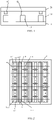
Fig. 1 is a schematic structural diagram showing a display panel according to an embodiment of the present disclosure; -
Fig. 2 is a plan view showing common electrodes of an array substrate of a display panel according to an embodiment of the present disclosure; -
Fig. 2 is a plan view showing common electrodes of an array substrate of a display panel according to an embodiment of the present disclosure; -
Fig. 3 is a schematic diagram showing a plane structure of an array substrate and spacers of a display panel according to an embodiment of the present disclosure; -
Fig. 4 is a sectional view of a display panel along a line AA' inFig. 3 according to an embodiment of the present disclosure; -
Fig. 5 is a sectional view of a display panel along a line BB' inFig. 3 according to an embodiment of the present disclosure; -
Fig. 6 is a schematic diagram showing a plane structure of a color filter substrate and spacers according to an embodiment of the present disclosure; -
Fig. 7 is a schematic structural diagram showing a display panel according to another embodiment of the present disclosure; -
Fig. 8 is a schematic diagram illustrating a portion of a structure of a display substrate according to another embodiment of the present disclosure; -
Fig. 9 is a schematic diagram showing a plane structure of a color filter substrate and spacers according to another embodiment of the present disclosure; -
Fig. 10 is a schematic structural diagram showing a display panel according to still another embodiment of the present disclosure; -
Fig. 11 is a schematic diagram showing a portion of a structure of an array substrate according to still another embodiment of the present disclosure; -
Fig. 12 is a schematic diagram showing a plane structure of a color filter substrate and spacers according to still another embodiment of the present disclosure; and -
Fig. 13 is a schematic diagram showing a portion of a structure of an array substrate according to yet another embodiment of the present disclosure. - In order to enable those skilled in the art to better understand the technical solutions of the present disclosure, the present disclosure is further described in detailed below with reference to the accompanying drawings and the specific implementations.
- The embodiments of the present disclosure are described below, the examples of the embodiments are illustrated in the accompanying drawings, and the same or similar reference numerals refer to the same or similar elements, or elements having the same or similar functions throughout the present disclosure. The embodiments described below with reference to the accompanying drawings are exemplary, are only used to explain the present disclosure, and should not be understood to limit the present disclosure.
- In the present disclosure, a dimension of a spacer along a row direction is defined as a length, a dimension of the spacer along a direction perpendicular to the row direction in a plane parallel to a display panel is defined as a width, and a dimension of the spacer along a direction perpendicular to the display panel is defined as a height. Directions along the length, width, and height of the spacer are respectively referred to as a length direction, a width direction and a height direction. A section shape of the spacer along the height direction is referred to as a longitudinal section shape, and a section shape of the spacer along a plane parallel to the display panel is referred to as a cross-section shape.
- In the present disclosure, the row direction is a direction along which a gate line extends, and a column direction is a direction along which a data line extends.
- According to some embodiments of the present disclosure, a display panel includes an
array substrate 11, acolor filter substrate 21, aliquid crystal layer 31 and spacers packaged between thearray substrate 11 and thecolor filter substrate 21. Referring toFig. 1 ,first spacers 41 are disposed on thearray substrate 11, andsecond spacers 42 andthird spacers 43 are disposed facing thefirst spacers 41 on thecolor filter substrate 21. Thesecond spacers 42 and thethird spacers 43 overlap thefirst spacers 41 respectively. Thesecond spacer 42 is in contact with a surface of thefirst spacer 41, and there is a gap between thethird spacer 43 and thefirst spacer 41. That is, a height of thethird spacer 43 is smaller than that of thesecond spacer 42, so as to ensure that thefirst spacer 41 is in contact with a surface of thesecond spacer 42. The heights of the first spacer, the second spacer and the third spacers are all in the range of 1µm to 2µm.The cross-section shapes and the longitudinal section shapes of thefirst spacer 41, thesecond spacer 42, and thethird spacer 43 are not limited herein. For example, thefirst spacer 41, thesecond spacer 42, and thethird spacer 43 may have a circular, oval, or rectangular cross-section shape, and have a rectangular longitudinal section shape. In general, the spacers are disposed between thearray substrate 11 and thecolor filter substrate 21, so that a gap between thearray substrate 11 and thecolor filter substrate 21 can be controlled to maintain an optimal thickness of the liquid crystal layer. According to some embodiments of the present disclosure, the spacers are respectively disposed on the array substrate and the color filter substrate, which may prevent a large deformed area of the color filter substrate during touch operations and avoid an influence on the touch detection precision. - According to some embodiments of the present disclosure, for a display panel with a touch function, the array substrate thereof is provided with common electrodes. At least a part of the common electrode also function as touch electrodes, that is, those electrodes are used as touch electrodes when receiving a touch action, and are used as common electrodes when no touch action is received. In order to make it easy to distinguish, a common electrode with a touch driving function and an auxiliary electrode located thereon are referred to as a driving electrode, and a common electrode with a touch sensing function and an auxiliary electrode located thereon are referred to as a sensing electrode in the present disclosure. The auxiliary electrodes of the driving electrode and the sensing electrode are described in detail below.
- Referring to
Fig. 2 to Fig. 4 , an arrangement of common electrodes of an array substrate of a display panel is described below. According to whether a common electrode is shared, thearray substrate 11 is divided into a plurality of drivingelectrode regions 1140 and a plurality of sensingelectrode regions 1150, which are alternately arranged in a row direction,. A shared common electrode is disposed in each drivingelectrode region 1140 and eachsensing electrode region 1150. Each drivingelectrode region 1140 is provided with a firstcommon electrode 116, and eachsensing electrode region 1150 is provided with a secondcommon electrode 117. The drivingelectrode regions 1140 are discontinuous from each other along a column direction, and thesensing electrode regions 1150 are uninterrupted or continuous along the column direction. Sensing electrode lines are disposed on the secondcommon electrode 117 in thesensing electrode region 1150, and include a transversesensing electrode line 1151 and a longitudinalsensing electrode line 1152 which are connected with each other. Moreover, in order to obtain a uniform electric field, dummy sensing electrode lines are further provided on the firstcommon electrode 116 in the drivingelectrode region 1140, and include a dummy transversesensing electrode line 1141 and a dummy longitudinalsensing electrode line 1142 which are connected with each other. In the present disclosure, the secondcommon electrode 117, and the transversesensing electrode line 1151 and the longitudinalsensing electrode line 1152 located on the secondcommon electrode 117 are referred to as asensing electrode 115, and the firstcommon electrode 116, and the dummy transversesensing electrode line 1141 and the longitudinal dummydummy longitudinalsensing electrode line 1142 located on the first common electrode are referred to as a drivingelectrode 114. The dummy longitudinalsensing electrode line 1142 and the dummy transversesensing electrode line 1141 are disposed in the same layer as the longitudinalsensing electrode line 1152 and the transversesensing electrode line 1151. The dummy longitudinalsensing electrode line 1142 and the dummy transversesensing electrode line 1141 are directly connected with the firstcommon electrode 116, and the longitudinalsensing electrode line 1152 and the transversesensing electrode line 1151 are directly connected with the secondcommon electrode 117. The dummy longitudinalsensing electrode line 1142 and the dummy transversesensing electrode line 1141 in the drivingelectrode regions 1140 are disconnected from the longitudinalsensing electrode line 1152 and the transversesensing electrode line 1151 in thesensing electrode regions 1150, and the dummy longitudinalsensing electrode lines 1142 in the drivingelectrode regions 1140 adjacent along the column direction are disconnected from each other. Drivingelectrode lines 113 in the drivingelectrode regions 1140 and thesensing electrode regions 1150 are connected with each other along the row direction. - The array substrate includes a plurality of pixel units arranged along a plurality of rows and a plurality of columns. A plurality of
data lines 112 are disposed between the plurality of columns of pixel units along the column direction, a plurality ofgate lines 111 are disposed between the plurality of rows of pixel units along the row direction, and the drivingelectrode lines 113 are located in a gate layer of the pixel units and are parallel to the gate lines. Thefirst spacer 41 is located above thedata line 112, and is located above a position between thegate line 111 and the drivingelectrode line 113. In some embodiments, an orthographic projection of thefirst spacer 41 on the array substrate may overlap both an orthographic projection of the gate line on the substrate and an orthographic projection of the driving electrode line on the substrate, and meanwhile overlap an orthographic projection of thedata line 112 on the substrate. In some embodiments, an orthographic projection of thefirst spacer 41 on the array substrate is located between the orthographic projections, on the array substrate, of the drivingelectrode line 113 andgate line 111 that are adjacent to each other and overlaps an orthographic projection of thedata line 112 on the array substrate. - Meanwhile, in the driving electrode region, the
first spacer 41 are also located above thedata line 112, and is located above a position between thegate line 111 and dummy transversesensing electrode line 1141 that are adjacent to each other. - In some embodiments, the
first spacer 41 is located between orthographic projections, on the array substrate, of thegate line 111 and dummy transversesensing electrode line 1141 that are adjacent to each other and overlaps an orthographic projection of thedata line 112 on the array substrate. In some embodiments, an orthographic projection of thefirst spacer 41 on the array substrate overlaps both an orthographic projection of thegate line 111 and the dummy transversesensing electrode line 1141 on the array substrate respectively, and further overlaps an orthographic projection of thedata line 112 on the array substrate. - In the sensing electrode region, the
first spacer 41 is also located above thedata line 112, and is located above a position between thegate line 111 and transversesensing electrode line 1151 that are adjacent to each other. - In some embodiments, the
first spacer 41 is located between orthographic projections, on the array substrate, of thegate line 111 and transversesensing electrode line 1151 that are adjacent to each other and overlaps an orthographic projection of thedata line 112 on the array substrate. In some embodiments, an orthographic projection of thefirst spacer 41 on the array substrate overlaps orthographic projections of thegate line 111 and the transversesensing electrode line 1151 on the array substrate, respectively, and further overlaps an orthographic projection of thedata line 112 on the array substrate. - The common electrode located in the driving electrode region is connected to the driving
electrode line 113 through a first via 1101. -
Fig. 4 is a cross-sectional view of an array substrate along a line AA' inFig. 3 . Referring toFig. 4 , in the drivingelectrode region 1140, the drivingelectrode 114 includes the dummy transversesensing electrode line 1141 and and the dummy longitudinalsensing electrode line 1142, wherein the dummy transversesensing electrode line 1141 is disposed on the firstcommon electrode 116 and extends along the row direction; and the dummy longitudinalsensing electrode line 1142 is disposed on the firstcommon electrode 116, extends along the column direction, and is connected with the dummy transversesensing electrode line 1141. Meanwhile, the driving electrodes 114 (or the first common electrodes 116) in the same row are connected with the drivingelectrode line 113 through thefirst vias 1101. In the drivingelectrode region 1140, an orthographic projection of thefirst spacer 41 on the array substrate is located within an orthographic projection of the drivingelectrode 114 on the array substrate. -
Fig. 5 is a sectional view of an array substrate along a line BB' inFig. 3 . Referring toFig. 5 , in thesensing electrode region 1150, thesensing electrode 115 further includes the transversesensing electrode line 1151 and the longitudinalsensing electrode line 1152, wherein the transversesensing electrode line 1151 is disposed on the secondcommon electrode 117 and extends along the row direction; and the longitudinalsensing electrode line 1152 is disposed on the secondcommon electrode 117, extends along the column direction, and is connected with the transversesensing electrode line 1151. In thesensing electrode region 1150, an orthographic projection of thefirst spacer 41 on the array substrate is located within an orthographic projection of thesensing electrode 115 on the array substrate. - According to an embodiment of the present disclosure, a
slit pixel electrode 118 is provided on the firstcommon electrode 116 or the secondcommon electrode 117, and an insulating layer is further formed between theslit pixel electrode 118 and the firstcommon electrode 116 or the secondcommon electrode 117. - According to an embodiment of the present disclosure, spacers are disposed both on the
array substrate 11 and thecolor filter substrate 21. Referring toFig. 6 ,second spacers 42 andthird spacers 43 are disposed on thecolor filter substrate 21 at positions corresponding to thefirst spacers 41. The arrangement of thesecond spacers 42 and thethird spacers 43 is not limited herein. In some embodiments, thesecond spacers 42 and thethird spacers 43 are disposed at intervals along the row direction. - The cross-section shapes of the
first spacers 41, thesecond spacers 42, and thethird spacers 43 are not limited herein, and may be, for example, rectangular, oval, or circular. The longitudinal section shapes of thefirst spacers 41, thesecond spacers 42, and thethird spacers 43 may be rectangular. - According to other embodiments of the present disclosure, the spacers may be arranged in different ways. Referring to
Fig. 7 , the longitudinal section shape of thefirst spacer 41 on thearray substrate 11 is in a shape of rectangle, a long side of the rectangle is a side extending along a length direction of the first spacer, and thefirst spacer 41 extends along the length direction beyond a distance between the adjacent data lines. A length L1 of thefirst spacer 41 spans at least one pixel unit, and is greater than the distance between the adjacent data lines, and is also greater than a length of thesecond spacer 42 and a length of thethird spacer 43. In some embodiments, the length L1 of the first spacer spans two pixel units. In the present embodiment, the lengths of thesecond spacer 42 and thethird spacer 43 may not be limited thereto. The length L2 of thesecond spacer 42 may be different from or the same as the length L3 of thethird spacer 43. - In the present embodiment, each of the first spacers corresponds to a plurality of second and third spacers, so that alignment between the array substrate and the color filter substrate is simpler and more convenient.
-
Fig. 8 shows a position of thefirst spacer 41 on the array substrate in the present embodiment. Thefirst spacer 41 may be disposed in the driving electrode region at a position between thegate line 111 and dummy transversesensing electrode line 1141 that are adjacent to each other, or a position between thegate line 111 and drivingelectrode line 113 that are adjacent to each other. Accordingly, in the sensing electrode region, the first spacer may be disposed at a position between thegate line 111 and transversesensing electrode line 1151 that are adjacent to each other, or a position between thegate line 111 and drivingelectrode line 113 that are adjacent to each other. - In some embodiments, referring to
Fig. 9 , the widths of thefirst spacers 41, thesecond spacers 42 and thethird spacers 43 are not limited. A width W2 of thesecond spacer 42 may be the same as or different from a width W3 of thethird spacer 43. - The cross-section shapes of the
first spacers 41, thesecond spacers 42, and thethird spacers 43 are not limited herein, and may be, for example, rectangular, oval, or circular. The longitudinal section shapes of thefirst spacers 41, thesecond spacers 42, and thethird spacers 43 may be rectangular. The cross-section shape of thesecond spacers 42 and thethird spacers 43 are rectangular inFig. 9 , and the cross-section shape of thesecond spacers 42 and thethird spacers 43 are circular inFig. 6 . - According to other embodiments of the present disclosure, referring to
Fig. 10 , each of the length L2 of thesecond spacer 42 and the length L3 of thethird spacer 43 is greater than the length L1 of thefirst spacer 41. Meanwhile, each of the width W2 of thesecond spacer 42 and the width W3 of thethird spacer 43 is smaller than the width W1 of the first spacer 41 (not shown inFig. 10 ). -
Fig. 11 shows the positions of the first spacers on the array substrate in the present embodiment. In the driving electrode region, thefirst spacer 41 is disposed at a position between thegate line 111 and dummy transversesensing electrode line 1141 that are adjacent to each other and overlaps the data line, or disposed at a position between thegate line 111 and drivingelectrode line 113 that are adjacent to each other and overlaps the data line. In the sensing electrode region, the first spacer is disposed at a position between thegate line 111 and transverse sensing electrode line that are adjacent to each other and overlaps thedata line 112, or disposed at a position between thegate line 111 and drivingelectrode line 113 that are adjacent to each other and overlaps thedata line 112. - According to an embodiment of the present disclosure, the spacers are disposed both on the
array substrate 11 and thecolor filter substrate 21. Referring toFig. 12 , thesecond spacers 42 and thethird spacers 43 are provided on thecolor filter substrate 21 at positions corresponding to thefirst spacers 41. The arrangement of thesecond spacers 42 and thethird spacers 43 is not limited herein. In some embodiments, thesecond spacers 42 and thethird spacers 43 are disposed at intervals. - In the present embodiment, the widths of the
second spacers 42 and thethird spacers 43 are not specifically limited, and for example, the width W2 of thesecond spacer 42 and the width W3 of thethird spacer 43 are different from the width W1 of thefirst spacer 41. - The cross-section shapes of the
first spacers 41, thesecond spacers 42, and thethird spacers 43 are not limited herein, and may be, for example, rectangular, oval, or circular. The longitudinal section shapes of thefirst spacers 41, thesecond spacers 42, and thethird spacers 43 may be rectangular. The cross-section shapes of thesecond spacers 42 and thethird spacers 43 are oval inFig. 12 . - According to some embodiments of the present disclosure, referring to
Fig. 13 , no longitudinalsensing electrode line 1152 or dummy longitudinalsensing electrode line 1142 is provided on a data line 112 (also referred to as an intermediate data line) at the boundary between a drivingelectrode region 1140 and asensing electrode region 1150, so as to separate the drivingelectrode region 1140 from thesensing electrode region 1150. Thefirst spacers 41 are disposed at the position of the intermediate data line. Meanwhile, in order to achieve uniform distribution of a touch electric field on the array substrate, thefirst spacers 41 are also disposed at and only at the positions of the data lines connected with the pixel units having the same color as that of the pixel units connected with the intermediate data line. For example, if the intermediate data line at the boundary between the drivingelectrode region 1140 and thesensing electrode region 1150 is connected with red pixel units, thefirst spacers 41 are only disposed at the positions of the data lines connected with all red sub-pixel units, and nofirst spacer 41 is disposed on the data lines connected with other color pixel units, such as green pixel units and blue pixel units. - According to some embodiments of the present disclosure, the
first spacers 41, thesecond spacers 42, and thethird spacers 43 are all made of a resin material. Each of the heights of the first spacers, the second spacers, and the third spacers is in a range of 1µm to 2µm. - According to some embodiments of the present disclosure, the gate lines, the data lines, the driving electrodes and the sensing electrodes may be made of a metal material such as Cu, Al, Mo, Ti, Cr, and W, or the alloys thereof, and may have a single-layer structure, or a multi-layer structure, such as Mo\Al\Mo, Ti\Cu\Ti, and MoTi\Cu. The common electrodes and the slit pixel electrodes may be made of ITO.
- According to another aspect of the present disclosure, the present disclosure provides a display device including the above display panel.
- In the Description of the present disclosure, the term "one embodiment", "another embodiment" or the like indicates that the specific feature, structure, material, or characteristic described in conjunction with such embodiment is included in at least one embodiment of the present disclosure. In the Description, the illustration of the above term is not necessarily intended to refer to the same embodiment or example. Furthermore, the specifically described features, structures, materials, or characteristics may be combined in any suitable manner in any one or more embodiments or examples. Moreover, those skilled in the art can combine the various embodiments or examples and the features therein that are described in the Description if no conflict is incurred.
- It should be understood that the above embodiments are merely exemplary embodiments employed to illustrate the principles of the present disclosure, and the present disclosure is not limited thereto. Various changes, modifications, substitutions and variations can be made by those skilled in the art without departing from the spirit and essence of the present disclosure, and should be considered to fall within the scope of the present disclosure.
Claims (16)
- A display panel, comprising an array substrate, a color filter substrate, a liquid crystal layer and a plurality of spacers located between the array substrate and the color filter substrate, whereinthe plurality of spacers comprise at least one first spacer, at least one second spacer and at least one third spacer,the at least one first spacer is on the array substrate,the at least one second spacer and the at least one third spacer are on the color filter substrate and respectively overlap the at least one first spacer in a direction perpendicular to the display panel, andthe at least one first spacer, the at least one second spacer and the at least one third spacer have a first height, a second height and a third height respectively along the direction perpendicular to the display panel, with the second height different from the third height.
- The display panel of claim 1, whereinthe array substrate is divided into a plurality of driving electrode regions and a plurality of sensing electrode regions alternately arranged along a row direction,the sensing electrode regions are continuous along a column direction,each column of the plurality of driving electrode regions comprises multiple driving electrode regions,each of the plurality of driving electrode region is provided with a first common electrode, and each of the plurality of sensing electrode region is provided with a second common electrode,at least one driving electrode line is within the plurality of driving electrode regions and the plurality of sensing electrode regions alternately arranged along the row direction, and continuously extends along the row direction through driving electrode regions and sensing electrode regions in a same row, andthe first common electrode in the driving electrode region is connected with the driving electrode line through at least one first via.
- The display panel of claim 2, whereinthe array substrate comprises a plurality of pixel units arranged along a plurality of rows and a plurality of columns,a plurality of data lines are disposed between the plurality of columns of pixel units along the column direction,a plurality of gate lines are disposed between the plurality of rows of pixel units along the row direction,the driving electrode line is in parallel with the gate lines, andthe first spacer is on the array substrate at a position between orthographic projections of the driving electrode line and the gate line that are adjacent to each other on the array substrate, and overlaps an orthographic projection of the data line on the array sub strate.
- The display panel of claim 2, whereinthe array substrate comprises a plurality of pixel units arranged along a plurality of rows and a plurality of columns,a plurality of data lines are disposed between the plurality of columns of pixel units along the column direction,a plurality of gate lines are disposed between the plurality of rows of pixel units along the row direction,the driving electrode line is in parallel with the gate lines, andan orthographic projection of the first spacer on the array substrate overlaps both orthographic projections of the gate line and the driving electrode line on the array substrate, and further overlaps an orthographic projection of the data line on the array sub strate.
- The display panel of claim 2, whereinthe array substrate comprises a plurality of pixel units arranged along a plurality of rows and a plurality of columns,a plurality of data lines are disposed between the plurality of columns of pixel units along the column direction,a plurality of gate lines are disposed between the plurality of rows of pixel units along the row direction,the driving electrode region is provided therein with at least one dummy transverse sensing electrode line and at least one dummy longitudinal sensing electrode line, with the at least one dummy transverse sensing electrode line being in parallel with the gate lines, and the at least one dummy longitudinal sensing electrode line being in parallel with the data lines and connected with the at least one dummy transverse sensing electrode line, andthe first spacer is on the array substrate at a position between orthographic projections of the gate line and dummy transverse sensing electrode line that are adjacent to each other on the array substrate, and overlaps an orthographic projection of the data line on the array substrate.
- The display panel of claim 2, whereinthe array substrate comprises a plurality of pixel units arranged along a plurality of rows and a plurality of columns,a plurality of data lines are disposed between the plurality of columns of pixel units along the column direction,a plurality of gate lines are disposed between the plurality of rows of pixel units along the row direction,the driving electrode region is provided therein with at least one dummy transverse sensing electrode line and at least one dummy longitudinal sensing electrode line, with the at least one dummy transverse sensing electrode line being in parallel with the gate lines, and the at least one dummy longitudinal sensing electrode line being in parallel with the data lines and connected with the at least one dummy transverse sensing electrode line, andan orthographic projection of the first spacer on the array substrate overlaps both an orthographic projection of the gate line on the array substrate and an orthographic projection of the dummy transverse sensing electrode line on the array substrate, and further overlaps an orthographic projection of the data line on the array substrate.
- The display panel of claim 2, whereinthe array substrate comprises a plurality of pixel units arranged along a plurality of rows and a plurality of columns,a plurality of data lines are disposed between the plurality of columns of pixel units along the column direction,a plurality of gate lines are disposed between the plurality of rows of pixel units along the row direction,the sensing electrode region is provided therein with at least one transverse sensing electrode line and at least one longitudinal sensing electrode line, with the at least one transverse sensing electrode line being in parallel with the gate lines, and the at least one longitudinal sensing electrode line being in parallel with the data lines and connected with the at least one transverse sensing electrode line, andthe first spacer is on the array substrate at a position between orthographic projections of the gate line and transverse sensing electrode line that are adjacent to each other on the array substrate, and overlaps an orthographic projection of the data line on the array substrate.
- The display panel of claim 2, whereinthe array substrate comprises a plurality of pixel units arranged along a plurality of rows and a plurality of columns,a plurality of data lines are disposed between the plurality of columns of pixel units along the column direction,a plurality of gate lines are disposed between the plurality of rows of pixel units along the row direction,the sensing electrode region is provided therein with at least one transverse sensing electrode line and at least one longitudinal sensing electrode line, with the at least one transverse sensing electrode line being in parallel with the gate lines, and the at least one longitudinal sensing electrode line being in parallel with the data lines and connected with the at least one transverse sensing electrode line, andan orthographic projection of the first spacer on the array substrate overlaps both of an orthographic projection of the gate line on the array substrate and an orthographic projection of the transverse sensing electrode line on the array substrate, and further overlaps an orthographic projection of the data line on the array substrate.
- The display panel of claim 2, whereinthe array substrate comprises a plurality of pixel units arranged along a plurality of rows and a plurality of columns,a plurality of data lines are disposed between the plurality of columns of pixel units along the column direction,a plurality of gate lines are disposed between the plurality of rows of pixel units along the row direction,no longitudinal sensing electrode line or dummy longitudinal sensing electrode line is disposed on an intermediate data line at a boundary between the driving electrode region and the sensing electrode region,in the driving electrode region or the sensing electrode region, no longitudinal sensing electrode line or dummy longitudinal sensing electrode line is disposed on data lines connected with pixel units having the same color as that of pixel units connected to the intermediate data line, andamong all the data lines, the first spacer is only on the intermediate data line and the data lines on which no longitudinal sensing electrode line or dummy longitudinal sensing electrode line is disposed.
- The display panel of claim 1, wherein the first spacer, the second spacer, and the third spacer have rectangular, circular, or oval cross-section shape in a plane where the array substrate is located.
- The display panel of claim 1, wherein a first length of the first spacer along a row direction is greater than a second length of the second spacer along the row direction, and is also greater than a third length of the third spacer along the row direction.
- The display panel of claim 1, whereinthe array substrate comprises a plurality of pixel units arranged along a plurality of rows and a plurality of columns,the first spacer has a first length along a row direction, andthe first length is greater than a distance between adjacent data lines, greater than a second length of the second spacer along the row direction, and also greater than a third length of the third spacer along the row direction.
- The display panel of claim 12, wherein the first length of the first spacer spans two pixel units.
- The display panel of claim 1, whereineach of a second length of the second spacer along a row direction and a third length of the third spacer along the row direction is greater than a first length of the first spacer along the row direction, andeach of a second width of the second spacer and a third width of the third spacer is smaller than a first width of the first spacer.
- The display panel of claim 1, wherein each of the heights of the first spacer, the second spacer, and the third spacer is in a range of 1µm to 2µm.
- A display device, comprising the display panel of any of claims 1 to 15.
Applications Claiming Priority (1)
| Application Number | Priority Date | Filing Date | Title |
|---|---|---|---|
| PCT/CN2019/097690 WO2021012258A1 (en) | 2019-07-25 | 2019-07-25 | Display panel and display device |
Publications (3)
| Publication Number | Publication Date |
|---|---|
| EP4006634A1 true EP4006634A1 (en) | 2022-06-01 |
| EP4006634A4 EP4006634A4 (en) | 2022-10-19 |
| EP4006634B1 EP4006634B1 (en) | 2024-09-04 |
Family
ID=71856303
Family Applications (1)
| Application Number | Title | Priority Date | Filing Date |
|---|---|---|---|
| EP19930171.4A Active EP4006634B1 (en) | 2019-07-25 | 2019-07-25 | Display panel and display device |
Country Status (4)
| Country | Link |
|---|---|
| US (1) | US11852925B2 (en) |
| EP (1) | EP4006634B1 (en) |
| CN (1) | CN211207023U (en) |
| WO (1) | WO2021012258A1 (en) |
Families Citing this family (1)
| Publication number | Priority date | Publication date | Assignee | Title |
|---|---|---|---|---|
| KR20250104635A (en) * | 2023-12-29 | 2025-07-08 | 엘지디스플레이 주식회사 | Light emitting display apparatus |
Family Cites Families (13)
| Publication number | Priority date | Publication date | Assignee | Title |
|---|---|---|---|---|
| KR101347291B1 (en) * | 2006-11-17 | 2014-01-03 | 삼성디스플레이 주식회사 | Flat panel display with a built-in touch sensor, method for driving the same and flat panel display device having the same |
| KR20100024751A (en) * | 2008-08-26 | 2010-03-08 | 삼성전자주식회사 | LCD and its manufacturing method |
| TWI408449B (en) * | 2009-11-03 | 2013-09-11 | Wintek Corp | Liquid crystal display panel |
| KR101790977B1 (en) * | 2010-10-08 | 2017-10-26 | 엘지디스플레이 주식회사 | Liquid crystal display device |
| WO2012176966A1 (en) | 2011-06-20 | 2012-12-27 | Melfas, Inc. | Touch sensor panel |
| EP2538313B1 (en) | 2011-06-20 | 2015-05-20 | Melfas, Inc. | Touch sensor panel |
| CN102243397A (en) * | 2011-07-05 | 2011-11-16 | 深圳市华星光电技术有限公司 | Liquid crystal panel and spacer structure thereof |
| JP2013186148A (en) * | 2012-03-06 | 2013-09-19 | Japan Display West Co Ltd | Liquid crystal display device, method of manufacturing liquid crystal display device, and electronic equipment |
| CN103760708B (en) * | 2014-01-09 | 2017-08-11 | 北京京东方光电科技有限公司 | A kind of array base palte, capacitive touch screen and touch control display apparatus |
| KR20160001794A (en) * | 2014-06-26 | 2016-01-07 | 삼성디스플레이 주식회사 | Liquid crystal display panel |
| KR102229505B1 (en) * | 2015-01-09 | 2021-03-18 | 삼성디스플레이 주식회사 | Liquid crystal display and method for manufacturing the same |
| US20170242286A1 (en) * | 2016-02-19 | 2017-08-24 | Apple Inc. | Display Having Column Spacer Structures with Minimized Plastic Deformation |
| CN106597759B (en) | 2017-02-24 | 2019-06-28 | 京东方科技集团股份有限公司 | Spacer, display substrate and manufacturing method thereof, and display panel |
-
2019
- 2019-07-25 WO PCT/CN2019/097690 patent/WO2021012258A1/en not_active Ceased
- 2019-07-25 EP EP19930171.4A patent/EP4006634B1/en active Active
- 2019-07-25 CN CN201990000086.4U patent/CN211207023U/en active Active
- 2019-07-25 US US16/963,197 patent/US11852925B2/en active Active
Also Published As
| Publication number | Publication date |
|---|---|
| EP4006634B1 (en) | 2024-09-04 |
| US20210405419A1 (en) | 2021-12-30 |
| EP4006634A4 (en) | 2022-10-19 |
| US11852925B2 (en) | 2023-12-26 |
| CN211207023U (en) | 2020-08-07 |
| WO2021012258A1 (en) | 2021-01-28 |
Similar Documents
| Publication | Publication Date | Title |
|---|---|---|
| US9507230B2 (en) | Array substrate, liquid crystal panel and liquid crystal display | |
| US11740523B2 (en) | Display panel and display device | |
| EP2755077B1 (en) | Colour film substrate and capacitive touch screen | |
| US9874959B2 (en) | Array substrate, touch control display device and touch control driving method | |
| US9766514B2 (en) | Liquid crystal display device with gap spacer and push spacer and method of fabricating the same | |
| EP3321730B1 (en) | Array substrate and manufacturing method thereof and display device | |
| US10223954B2 (en) | Array substrate and method for manufacturing the same, and display apparatus | |
| JP2013125277A (en) | Liquid crystal display element and method for manufacturing the same | |
| CN104914630A (en) | Array substrate, display panel and display device | |
| US20250224634A1 (en) | Array substrate and manufacturing method, display panel, and display device | |
| WO2022193337A1 (en) | Array substrate and display panel | |
| JP4092309B2 (en) | Liquid crystal display | |
| JP2009109658A (en) | Liquid crystal display device and manufacturing method thereof | |
| US11852925B2 (en) | Display panel and display device having spacers with different heights | |
| JP5610411B2 (en) | Liquid crystal display device and manufacturing method thereof | |
| US20210165516A1 (en) | Display panel and display device | |
| EP4006631B1 (en) | Array substrate and liquid crystal display | |
| US6812987B2 (en) | IPS-LCD with a compensation structure for reducing transmittance difference | |
| CN113934064B (en) | Array substrate, liquid crystal display panel and display device | |
| JP4935434B2 (en) | Liquid crystal display | |
| CN117518646A (en) | Array substrate, display panel and display device |
Legal Events
| Date | Code | Title | Description |
|---|---|---|---|
| STAA | Information on the status of an ep patent application or granted ep patent |
Free format text: STATUS: UNKNOWN |
|
| STAA | Information on the status of an ep patent application or granted ep patent |
Free format text: STATUS: THE INTERNATIONAL PUBLICATION HAS BEEN MADE |
|
| PUAI | Public reference made under article 153(3) epc to a published international application that has entered the european phase |
Free format text: ORIGINAL CODE: 0009012 |
|
| STAA | Information on the status of an ep patent application or granted ep patent |
Free format text: STATUS: REQUEST FOR EXAMINATION WAS MADE |
|
| 17P | Request for examination filed |
Effective date: 20201203 |
|
| AK | Designated contracting states |
Kind code of ref document: A1 Designated state(s): AL AT BE BG CH CY CZ DE DK EE ES FI FR GB GR HR HU IE IS IT LI LT LU LV MC MK MT NL NO PL PT RO RS SE SI SK SM TR |
|
| RIC1 | Information provided on ipc code assigned before grant |
Ipc: G06F 3/044 20060101ALI20220524BHEP Ipc: G06F 3/041 20060101ALI20220524BHEP Ipc: G02F 1/1339 20060101AFI20220524BHEP |
|
| A4 | Supplementary search report drawn up and despatched |
Effective date: 20220916 |
|
| RIC1 | Information provided on ipc code assigned before grant |
Ipc: G06F 3/044 20060101ALI20220912BHEP Ipc: G06F 3/041 20060101ALI20220912BHEP Ipc: G02F 1/1339 20060101AFI20220912BHEP |
|
| DAV | Request for validation of the european patent (deleted) | ||
| DAX | Request for extension of the european patent (deleted) | ||
| GRAP | Despatch of communication of intention to grant a patent |
Free format text: ORIGINAL CODE: EPIDOSNIGR1 |
|
| STAA | Information on the status of an ep patent application or granted ep patent |
Free format text: STATUS: GRANT OF PATENT IS INTENDED |
|
| INTG | Intention to grant announced |
Effective date: 20240423 |
|
| GRAS | Grant fee paid |
Free format text: ORIGINAL CODE: EPIDOSNIGR3 |
|
| GRAA | (expected) grant |
Free format text: ORIGINAL CODE: 0009210 |
|
| STAA | Information on the status of an ep patent application or granted ep patent |
Free format text: STATUS: THE PATENT HAS BEEN GRANTED |
|
| AK | Designated contracting states |
Kind code of ref document: B1 Designated state(s): AL AT BE BG CH CY CZ DE DK EE ES FI FR GB GR HR HU IE IS IT LI LT LU LV MC MK MT NL NO PL PT RO RS SE SI SK SM TR |
|
| REG | Reference to a national code |
Ref country code: GB Ref legal event code: FG4D |
|
| REG | Reference to a national code |
Ref country code: CH Ref legal event code: EP |
|
| REG | Reference to a national code |
Ref country code: IE Ref legal event code: FG4D |
|
| REG | Reference to a national code |
Ref country code: DE Ref legal event code: R096 Ref document number: 602019058543 Country of ref document: DE |
|
| REG | Reference to a national code |
Ref country code: LT Ref legal event code: MG9D |
|
| REG | Reference to a national code |
Ref country code: NL Ref legal event code: MP Effective date: 20240904 |
|
| PG25 | Lapsed in a contracting state [announced via postgrant information from national office to epo] |
Ref country code: NO Free format text: LAPSE BECAUSE OF FAILURE TO SUBMIT A TRANSLATION OF THE DESCRIPTION OR TO PAY THE FEE WITHIN THE PRESCRIBED TIME-LIMIT Effective date: 20241204 |
|
| PG25 | Lapsed in a contracting state [announced via postgrant information from national office to epo] |
Ref country code: PL Free format text: LAPSE BECAUSE OF FAILURE TO SUBMIT A TRANSLATION OF THE DESCRIPTION OR TO PAY THE FEE WITHIN THE PRESCRIBED TIME-LIMIT Effective date: 20240904 Ref country code: GR Free format text: LAPSE BECAUSE OF FAILURE TO SUBMIT A TRANSLATION OF THE DESCRIPTION OR TO PAY THE FEE WITHIN THE PRESCRIBED TIME-LIMIT Effective date: 20241205 Ref country code: FI Free format text: LAPSE BECAUSE OF FAILURE TO SUBMIT A TRANSLATION OF THE DESCRIPTION OR TO PAY THE FEE WITHIN THE PRESCRIBED TIME-LIMIT Effective date: 20240904 |
|
| PG25 | Lapsed in a contracting state [announced via postgrant information from national office to epo] |
Ref country code: BG Free format text: LAPSE BECAUSE OF FAILURE TO SUBMIT A TRANSLATION OF THE DESCRIPTION OR TO PAY THE FEE WITHIN THE PRESCRIBED TIME-LIMIT Effective date: 20240904 |
|
| PG25 | Lapsed in a contracting state [announced via postgrant information from national office to epo] |
Ref country code: LV Free format text: LAPSE BECAUSE OF FAILURE TO SUBMIT A TRANSLATION OF THE DESCRIPTION OR TO PAY THE FEE WITHIN THE PRESCRIBED TIME-LIMIT Effective date: 20240904 |
|
| PG25 | Lapsed in a contracting state [announced via postgrant information from national office to epo] |
Ref country code: HR Free format text: LAPSE BECAUSE OF FAILURE TO SUBMIT A TRANSLATION OF THE DESCRIPTION OR TO PAY THE FEE WITHIN THE PRESCRIBED TIME-LIMIT Effective date: 20240904 |
|
| PG25 | Lapsed in a contracting state [announced via postgrant information from national office to epo] |
Ref country code: RS Free format text: LAPSE BECAUSE OF FAILURE TO SUBMIT A TRANSLATION OF THE DESCRIPTION OR TO PAY THE FEE WITHIN THE PRESCRIBED TIME-LIMIT Effective date: 20241204 Ref country code: ES Free format text: LAPSE BECAUSE OF FAILURE TO SUBMIT A TRANSLATION OF THE DESCRIPTION OR TO PAY THE FEE WITHIN THE PRESCRIBED TIME-LIMIT Effective date: 20240904 |
|
| PG25 | Lapsed in a contracting state [announced via postgrant information from national office to epo] |
Ref country code: RS Free format text: LAPSE BECAUSE OF FAILURE TO SUBMIT A TRANSLATION OF THE DESCRIPTION OR TO PAY THE FEE WITHIN THE PRESCRIBED TIME-LIMIT Effective date: 20241204 Ref country code: PL Free format text: LAPSE BECAUSE OF FAILURE TO SUBMIT A TRANSLATION OF THE DESCRIPTION OR TO PAY THE FEE WITHIN THE PRESCRIBED TIME-LIMIT Effective date: 20240904 Ref country code: NO Free format text: LAPSE BECAUSE OF FAILURE TO SUBMIT A TRANSLATION OF THE DESCRIPTION OR TO PAY THE FEE WITHIN THE PRESCRIBED TIME-LIMIT Effective date: 20241204 Ref country code: LV Free format text: LAPSE BECAUSE OF FAILURE TO SUBMIT A TRANSLATION OF THE DESCRIPTION OR TO PAY THE FEE WITHIN THE PRESCRIBED TIME-LIMIT Effective date: 20240904 Ref country code: HR Free format text: LAPSE BECAUSE OF FAILURE TO SUBMIT A TRANSLATION OF THE DESCRIPTION OR TO PAY THE FEE WITHIN THE PRESCRIBED TIME-LIMIT Effective date: 20240904 Ref country code: GR Free format text: LAPSE BECAUSE OF FAILURE TO SUBMIT A TRANSLATION OF THE DESCRIPTION OR TO PAY THE FEE WITHIN THE PRESCRIBED TIME-LIMIT Effective date: 20241205 Ref country code: FI Free format text: LAPSE BECAUSE OF FAILURE TO SUBMIT A TRANSLATION OF THE DESCRIPTION OR TO PAY THE FEE WITHIN THE PRESCRIBED TIME-LIMIT Effective date: 20240904 Ref country code: ES Free format text: LAPSE BECAUSE OF FAILURE TO SUBMIT A TRANSLATION OF THE DESCRIPTION OR TO PAY THE FEE WITHIN THE PRESCRIBED TIME-LIMIT Effective date: 20240904 Ref country code: BG Free format text: LAPSE BECAUSE OF FAILURE TO SUBMIT A TRANSLATION OF THE DESCRIPTION OR TO PAY THE FEE WITHIN THE PRESCRIBED TIME-LIMIT Effective date: 20240904 |
|
| REG | Reference to a national code |
Ref country code: AT Ref legal event code: MK05 Ref document number: 1720993 Country of ref document: AT Kind code of ref document: T Effective date: 20240904 |
|
| PG25 | Lapsed in a contracting state [announced via postgrant information from national office to epo] |
Ref country code: NL Free format text: LAPSE BECAUSE OF FAILURE TO SUBMIT A TRANSLATION OF THE DESCRIPTION OR TO PAY THE FEE WITHIN THE PRESCRIBED TIME-LIMIT Effective date: 20240904 |
|
| PG25 | Lapsed in a contracting state [announced via postgrant information from national office to epo] |
Ref country code: PT Free format text: LAPSE BECAUSE OF FAILURE TO SUBMIT A TRANSLATION OF THE DESCRIPTION OR TO PAY THE FEE WITHIN THE PRESCRIBED TIME-LIMIT Effective date: 20250106 Ref country code: IS Free format text: LAPSE BECAUSE OF FAILURE TO SUBMIT A TRANSLATION OF THE DESCRIPTION OR TO PAY THE FEE WITHIN THE PRESCRIBED TIME-LIMIT Effective date: 20250104 |
|
| PG25 | Lapsed in a contracting state [announced via postgrant information from national office to epo] |
Ref country code: RO Free format text: LAPSE BECAUSE OF FAILURE TO SUBMIT A TRANSLATION OF THE DESCRIPTION OR TO PAY THE FEE WITHIN THE PRESCRIBED TIME-LIMIT Effective date: 20240904 Ref country code: SM Free format text: LAPSE BECAUSE OF FAILURE TO SUBMIT A TRANSLATION OF THE DESCRIPTION OR TO PAY THE FEE WITHIN THE PRESCRIBED TIME-LIMIT Effective date: 20240904 |
|
| PG25 | Lapsed in a contracting state [announced via postgrant information from national office to epo] |
Ref country code: EE Free format text: LAPSE BECAUSE OF FAILURE TO SUBMIT A TRANSLATION OF THE DESCRIPTION OR TO PAY THE FEE WITHIN THE PRESCRIBED TIME-LIMIT Effective date: 20240904 Ref country code: AT Free format text: LAPSE BECAUSE OF FAILURE TO SUBMIT A TRANSLATION OF THE DESCRIPTION OR TO PAY THE FEE WITHIN THE PRESCRIBED TIME-LIMIT Effective date: 20240904 |
|
| PG25 | Lapsed in a contracting state [announced via postgrant information from national office to epo] |
Ref country code: CZ Free format text: LAPSE BECAUSE OF FAILURE TO SUBMIT A TRANSLATION OF THE DESCRIPTION OR TO PAY THE FEE WITHIN THE PRESCRIBED TIME-LIMIT Effective date: 20240904 |
|
| PG25 | Lapsed in a contracting state [announced via postgrant information from national office to epo] |
Ref country code: SK Free format text: LAPSE BECAUSE OF FAILURE TO SUBMIT A TRANSLATION OF THE DESCRIPTION OR TO PAY THE FEE WITHIN THE PRESCRIBED TIME-LIMIT Effective date: 20240904 Ref country code: IT Free format text: LAPSE BECAUSE OF FAILURE TO SUBMIT A TRANSLATION OF THE DESCRIPTION OR TO PAY THE FEE WITHIN THE PRESCRIBED TIME-LIMIT Effective date: 20240904 |
|
| REG | Reference to a national code |
Ref country code: DE Ref legal event code: R097 Ref document number: 602019058543 Country of ref document: DE |
|
| PG25 | Lapsed in a contracting state [announced via postgrant information from national office to epo] |
Ref country code: DK Free format text: LAPSE BECAUSE OF FAILURE TO SUBMIT A TRANSLATION OF THE DESCRIPTION OR TO PAY THE FEE WITHIN THE PRESCRIBED TIME-LIMIT Effective date: 20240904 |
|
| PLBE | No opposition filed within time limit |
Free format text: ORIGINAL CODE: 0009261 |
|
| STAA | Information on the status of an ep patent application or granted ep patent |
Free format text: STATUS: NO OPPOSITION FILED WITHIN TIME LIMIT |
|
| 26N | No opposition filed |
Effective date: 20250605 |
|
| PG25 | Lapsed in a contracting state [announced via postgrant information from national office to epo] |
Ref country code: SE Free format text: LAPSE BECAUSE OF FAILURE TO SUBMIT A TRANSLATION OF THE DESCRIPTION OR TO PAY THE FEE WITHIN THE PRESCRIBED TIME-LIMIT Effective date: 20240904 |
|
| PGFP | Annual fee paid to national office [announced via postgrant information from national office to epo] |
Ref country code: DE Payment date: 20250722 Year of fee payment: 7 |
|
| PGFP | Annual fee paid to national office [announced via postgrant information from national office to epo] |
Ref country code: FR Payment date: 20250725 Year of fee payment: 7 |
|
| REG | Reference to a national code |
Ref country code: CH Ref legal event code: H13 Free format text: ST27 STATUS EVENT CODE: U-0-0-H10-H13 (AS PROVIDED BY THE NATIONAL OFFICE) Effective date: 20260224 |
|
| PG25 | Lapsed in a contracting state [announced via postgrant information from national office to epo] |
Ref country code: LU Free format text: LAPSE BECAUSE OF NON-PAYMENT OF DUE FEES Effective date: 20250725 |
|
| GBPC | Gb: european patent ceased through non-payment of renewal fee |
Effective date: 20250725 |
|
| REG | Reference to a national code |
Ref country code: BE Ref legal event code: MM Effective date: 20250731 |
|
| PG25 | Lapsed in a contracting state [announced via postgrant information from national office to epo] |
Ref country code: GB Free format text: LAPSE BECAUSE OF NON-PAYMENT OF DUE FEES Effective date: 20250725 |
|
| PG25 | Lapsed in a contracting state [announced via postgrant information from national office to epo] |
Ref country code: BE Free format text: LAPSE BECAUSE OF NON-PAYMENT OF DUE FEES Effective date: 20250731 |
|
| PG25 | Lapsed in a contracting state [announced via postgrant information from national office to epo] |
Ref country code: CH Free format text: LAPSE BECAUSE OF NON-PAYMENT OF DUE FEES Effective date: 20250731 |