EP4005675B1 - Verfahren zum herstellen von modularen vorrichtungen mit aktiver oberfläche fürmikrofluidische systeme - Google Patents
Verfahren zum herstellen von modularen vorrichtungen mit aktiver oberfläche fürmikrofluidische systeme Download PDFInfo
- Publication number
- EP4005675B1 EP4005675B1 EP22151888.9A EP22151888A EP4005675B1 EP 4005675 B1 EP4005675 B1 EP 4005675B1 EP 22151888 A EP22151888 A EP 22151888A EP 4005675 B1 EP4005675 B1 EP 4005675B1
- Authority
- EP
- European Patent Office
- Prior art keywords
- active surface
- substrate
- wafer
- microposts
- modular
- Prior art date
- Legal status (The legal status is an assumption and is not a legal conclusion. Google has not performed a legal analysis and makes no representation as to the accuracy of the status listed.)
- Active
Links
Images









Classifications
-
- B—PERFORMING OPERATIONS; TRANSPORTING
- B01—PHYSICAL OR CHEMICAL PROCESSES OR APPARATUS IN GENERAL
- B01L—CHEMICAL OR PHYSICAL LABORATORY APPARATUS FOR GENERAL USE
- B01L3/00—Containers or dishes for laboratory use, e.g. laboratory glassware; Droppers
- B01L3/50—Containers for the purpose of retaining a material to be analysed, e.g. test tubes
- B01L3/502—Containers for the purpose of retaining a material to be analysed, e.g. test tubes with fluid transport, e.g. in multi-compartment structures
- B01L3/5027—Containers for the purpose of retaining a material to be analysed, e.g. test tubes with fluid transport, e.g. in multi-compartment structures by integrated microfluidic structures, i.e. dimensions of channels and chambers are such that surface tension forces are important, e.g. lab-on-a-chip
- B01L3/502746—Containers for the purpose of retaining a material to be analysed, e.g. test tubes with fluid transport, e.g. in multi-compartment structures by integrated microfluidic structures, i.e. dimensions of channels and chambers are such that surface tension forces are important, e.g. lab-on-a-chip characterised by the means for controlling flow resistance, e.g. flow controllers, baffles or throttle valves
-
- B—PERFORMING OPERATIONS; TRANSPORTING
- B01—PHYSICAL OR CHEMICAL PROCESSES OR APPARATUS IN GENERAL
- B01L—CHEMICAL OR PHYSICAL LABORATORY APPARATUS FOR GENERAL USE
- B01L3/00—Containers or dishes for laboratory use, e.g. laboratory glassware; Droppers
- B01L3/50—Containers for the purpose of retaining a material to be analysed, e.g. test tubes
- B01L3/502—Containers for the purpose of retaining a material to be analysed, e.g. test tubes with fluid transport, e.g. in multi-compartment structures
- B01L3/5027—Containers for the purpose of retaining a material to be analysed, e.g. test tubes with fluid transport, e.g. in multi-compartment structures by integrated microfluidic structures, i.e. dimensions of channels and chambers are such that surface tension forces are important, e.g. lab-on-a-chip
- B01L3/502707—Containers for the purpose of retaining a material to be analysed, e.g. test tubes with fluid transport, e.g. in multi-compartment structures by integrated microfluidic structures, i.e. dimensions of channels and chambers are such that surface tension forces are important, e.g. lab-on-a-chip characterised by the manufacture of the container or its components
-
- B—PERFORMING OPERATIONS; TRANSPORTING
- B01—PHYSICAL OR CHEMICAL PROCESSES OR APPARATUS IN GENERAL
- B01L—CHEMICAL OR PHYSICAL LABORATORY APPARATUS FOR GENERAL USE
- B01L3/00—Containers or dishes for laboratory use, e.g. laboratory glassware; Droppers
- B01L3/50—Containers for the purpose of retaining a material to be analysed, e.g. test tubes
- B01L3/502—Containers for the purpose of retaining a material to be analysed, e.g. test tubes with fluid transport, e.g. in multi-compartment structures
- B01L3/5027—Containers for the purpose of retaining a material to be analysed, e.g. test tubes with fluid transport, e.g. in multi-compartment structures by integrated microfluidic structures, i.e. dimensions of channels and chambers are such that surface tension forces are important, e.g. lab-on-a-chip
- B01L3/502753—Containers for the purpose of retaining a material to be analysed, e.g. test tubes with fluid transport, e.g. in multi-compartment structures by integrated microfluidic structures, i.e. dimensions of channels and chambers are such that surface tension forces are important, e.g. lab-on-a-chip characterised by bulk separation arrangements on lab-on-a-chip devices, e.g. for filtration or centrifugation
-
- B—PERFORMING OPERATIONS; TRANSPORTING
- B01—PHYSICAL OR CHEMICAL PROCESSES OR APPARATUS IN GENERAL
- B01L—CHEMICAL OR PHYSICAL LABORATORY APPARATUS FOR GENERAL USE
- B01L3/00—Containers or dishes for laboratory use, e.g. laboratory glassware; Droppers
- B01L3/50—Containers for the purpose of retaining a material to be analysed, e.g. test tubes
- B01L3/502—Containers for the purpose of retaining a material to be analysed, e.g. test tubes with fluid transport, e.g. in multi-compartment structures
- B01L3/5027—Containers for the purpose of retaining a material to be analysed, e.g. test tubes with fluid transport, e.g. in multi-compartment structures by integrated microfluidic structures, i.e. dimensions of channels and chambers are such that surface tension forces are important, e.g. lab-on-a-chip
- B01L3/502761—Containers for the purpose of retaining a material to be analysed, e.g. test tubes with fluid transport, e.g. in multi-compartment structures by integrated microfluidic structures, i.e. dimensions of channels and chambers are such that surface tension forces are important, e.g. lab-on-a-chip specially adapted for handling suspended solids or molecules independently from the bulk fluid flow, e.g. for trapping or sorting beads or physically stretching molecules
-
- B—PERFORMING OPERATIONS; TRANSPORTING
- B01—PHYSICAL OR CHEMICAL PROCESSES OR APPARATUS IN GENERAL
- B01L—CHEMICAL OR PHYSICAL LABORATORY APPARATUS FOR GENERAL USE
- B01L2200/00—Solutions for specific problems relating to chemical or physical laboratory apparatus
- B01L2200/02—Adapting objects or devices to another
- B01L2200/026—Fluid interfacing between devices or objects, e.g. connectors, inlet details
- B01L2200/027—Fluid interfacing between devices or objects, e.g. connectors, inlet details for microfluidic devices
-
- B—PERFORMING OPERATIONS; TRANSPORTING
- B01—PHYSICAL OR CHEMICAL PROCESSES OR APPARATUS IN GENERAL
- B01L—CHEMICAL OR PHYSICAL LABORATORY APPARATUS FOR GENERAL USE
- B01L2200/00—Solutions for specific problems relating to chemical or physical laboratory apparatus
- B01L2200/02—Adapting objects or devices to another
- B01L2200/028—Modular arrangements
-
- B—PERFORMING OPERATIONS; TRANSPORTING
- B01—PHYSICAL OR CHEMICAL PROCESSES OR APPARATUS IN GENERAL
- B01L—CHEMICAL OR PHYSICAL LABORATORY APPARATUS FOR GENERAL USE
- B01L2200/00—Solutions for specific problems relating to chemical or physical laboratory apparatus
- B01L2200/12—Specific details about manufacturing devices
-
- B—PERFORMING OPERATIONS; TRANSPORTING
- B01—PHYSICAL OR CHEMICAL PROCESSES OR APPARATUS IN GENERAL
- B01L—CHEMICAL OR PHYSICAL LABORATORY APPARATUS FOR GENERAL USE
- B01L2200/00—Solutions for specific problems relating to chemical or physical laboratory apparatus
- B01L2200/16—Reagents, handling or storing thereof
-
- B—PERFORMING OPERATIONS; TRANSPORTING
- B01—PHYSICAL OR CHEMICAL PROCESSES OR APPARATUS IN GENERAL
- B01L—CHEMICAL OR PHYSICAL LABORATORY APPARATUS FOR GENERAL USE
- B01L2300/00—Additional constructional details
- B01L2300/04—Closures and closing means
- B01L2300/041—Connecting closures to device or container
-
- B—PERFORMING OPERATIONS; TRANSPORTING
- B01—PHYSICAL OR CHEMICAL PROCESSES OR APPARATUS IN GENERAL
- B01L—CHEMICAL OR PHYSICAL LABORATORY APPARATUS FOR GENERAL USE
- B01L2300/00—Additional constructional details
- B01L2300/06—Auxiliary integrated devices, integrated components
-
- B—PERFORMING OPERATIONS; TRANSPORTING
- B01—PHYSICAL OR CHEMICAL PROCESSES OR APPARATUS IN GENERAL
- B01L—CHEMICAL OR PHYSICAL LABORATORY APPARATUS FOR GENERAL USE
- B01L2300/00—Additional constructional details
- B01L2300/06—Auxiliary integrated devices, integrated components
- B01L2300/0627—Sensor or part of a sensor is integrated
- B01L2300/0645—Electrodes
-
- B—PERFORMING OPERATIONS; TRANSPORTING
- B01—PHYSICAL OR CHEMICAL PROCESSES OR APPARATUS IN GENERAL
- B01L—CHEMICAL OR PHYSICAL LABORATORY APPARATUS FOR GENERAL USE
- B01L2300/00—Additional constructional details
- B01L2300/06—Auxiliary integrated devices, integrated components
- B01L2300/0627—Sensor or part of a sensor is integrated
- B01L2300/0654—Lenses; Optical fibres
-
- B—PERFORMING OPERATIONS; TRANSPORTING
- B01—PHYSICAL OR CHEMICAL PROCESSES OR APPARATUS IN GENERAL
- B01L—CHEMICAL OR PHYSICAL LABORATORY APPARATUS FOR GENERAL USE
- B01L2300/00—Additional constructional details
- B01L2300/08—Geometry, shape and general structure
- B01L2300/0809—Geometry, shape and general structure rectangular shaped
- B01L2300/0816—Cards, e.g. flat sample carriers usually with flow in two horizontal directions
-
- B—PERFORMING OPERATIONS; TRANSPORTING
- B01—PHYSICAL OR CHEMICAL PROCESSES OR APPARATUS IN GENERAL
- B01L—CHEMICAL OR PHYSICAL LABORATORY APPARATUS FOR GENERAL USE
- B01L2300/00—Additional constructional details
- B01L2300/08—Geometry, shape and general structure
- B01L2300/0861—Configuration of multiple channels and/or chambers in a single devices
- B01L2300/0877—Flow chambers
-
- B—PERFORMING OPERATIONS; TRANSPORTING
- B01—PHYSICAL OR CHEMICAL PROCESSES OR APPARATUS IN GENERAL
- B01L—CHEMICAL OR PHYSICAL LABORATORY APPARATUS FOR GENERAL USE
- B01L2300/00—Additional constructional details
- B01L2300/08—Geometry, shape and general structure
- B01L2300/0861—Configuration of multiple channels and/or chambers in a single devices
- B01L2300/0883—Serpentine channels
-
- B—PERFORMING OPERATIONS; TRANSPORTING
- B01—PHYSICAL OR CHEMICAL PROCESSES OR APPARATUS IN GENERAL
- B01L—CHEMICAL OR PHYSICAL LABORATORY APPARATUS FOR GENERAL USE
- B01L2300/00—Additional constructional details
- B01L2300/08—Geometry, shape and general structure
- B01L2300/0887—Laminated structure
-
- B—PERFORMING OPERATIONS; TRANSPORTING
- B01—PHYSICAL OR CHEMICAL PROCESSES OR APPARATUS IN GENERAL
- B01L—CHEMICAL OR PHYSICAL LABORATORY APPARATUS FOR GENERAL USE
- B01L2300/00—Additional constructional details
- B01L2300/12—Specific details about materials
-
- B—PERFORMING OPERATIONS; TRANSPORTING
- B01—PHYSICAL OR CHEMICAL PROCESSES OR APPARATUS IN GENERAL
- B01L—CHEMICAL OR PHYSICAL LABORATORY APPARATUS FOR GENERAL USE
- B01L2400/00—Moving or stopping fluids
- B01L2400/08—Regulating or influencing the flow resistance
- B01L2400/084—Passive control of flow resistance
- B01L2400/086—Passive control of flow resistance using baffles or other fixed flow obstructions
-
- B—PERFORMING OPERATIONS; TRANSPORTING
- B01—PHYSICAL OR CHEMICAL PROCESSES OR APPARATUS IN GENERAL
- B01L—CHEMICAL OR PHYSICAL LABORATORY APPARATUS FOR GENERAL USE
- B01L2400/00—Moving or stopping fluids
- B01L2400/08—Regulating or influencing the flow resistance
- B01L2400/084—Passive control of flow resistance
- B01L2400/088—Passive control of flow resistance by specific surface properties
-
- B—PERFORMING OPERATIONS; TRANSPORTING
- B01—PHYSICAL OR CHEMICAL PROCESSES OR APPARATUS IN GENERAL
- B01L—CHEMICAL OR PHYSICAL LABORATORY APPARATUS FOR GENERAL USE
- B01L9/00—Supporting devices; Holding devices
- B01L9/52—Supports specially adapted for flat sample carriers, e.g. for plates, slides, chips
- B01L9/527—Supports specially adapted for flat sample carriers, e.g. for plates, slides, chips for microfluidic devices, e.g. used for lab-on-a-chip
Definitions
- the presently disclosed subject matter relates generally to the processing of biological materials and more particularly to modular active surface devices microfluidic system for microfluidic systems and methods of making same
- Microfluidic systems can include an active surface, which can be, for example, any surface or area (typically inside a reaction or assay chamber) that is used for processing biological materials.
- an active surface can be, for example, any surface or area (typically inside a reaction or assay chamber) that is used for processing biological materials.
- an active surface can be, for example, any surface or area (typically inside a reaction or assay chamber) that is used for processing biological materials.
- an active surface can be, for example, any surface or area (typically inside a reaction or assay chamber) that is used for processing biological materials.
- the modular active surface device for processing biological materials manufactured according to the method of the present invention comprises:
- the active surfaces of the modular active surface device are configured to manipulate a fluid inside the reaction chamber.
- the active surfaces comprise one or more elements selected from the group consisting of static surface-attached microposts, actuated surface-attached microposts, a microscale texture, a microscale topography, a system for physical perturbation of the first active surface, an electrical, electronic, and/or electromagnetic system, and an optically active surface.
- the system for physical perturbation of the first active surface is configured to perturb the first active surface by vibration or deformation.
- the optically active surface comprises elements selected from the group consisting of lenses, LEDs, and one or more materials that interact with external light sources.
- manipulation of the fluid inside the reaction chamber is selected from the group consisting of generating fluid flow, altering the flow profile of an externally driven fluid, fractionating a sample into constituent parts, establishing one or more concentration gradients, and eliminating one or more concentration gradients.
- the active surface substrates of the modular active surface device are rigid or semi-rigid plastic substrates.
- the active surfaces are micropost active surface layers comprising surface-attached microposts.
- the surface-attached microposts are arranged in arrays.
- the surface-attached microposts of the modular active surface device are configured for actuation in the presence of an actuation force.
- the actuation force is selected from the group consisting of a magnetic field, a thermal field, a sonic field, an optical field, an electrical field, and a vibrational field.
- the micropost active surfaces in the reaction chamber of the modular active surface device are configured for mixing operations, binding operations, and cell processing operations.
- the cell processing operations are selected from the group consisting of: cell concentration, cell collection, cell filtration, cell washing, cell counting, cell recovery, cell lysis, and cell de-clumping.
- the modular active surface device is configured to integrate into a microfluidics cartridge that comprises a recessed region configured to receive the modular active surface device.
- the microfluidics cartridge further comprises fluid lines set to correspond to the fluid port, wherein when microfluidics device receives the modular active surface device, the microfluidics device and the modular active surface device are fluidly coupled.
- the modular active surface device further comprises an adhesive layer for bonding to the microfluidics cartidge.
- the modular active surface device comprises microposts formed of an an active surface material.
- the active surface material is polydimethylsiloxane (PDMS).
- the microposts range in length from about 1 ⁇ m to about 100 ⁇ m. In another embodiment, the microposts range in diameter from about 0.1 ⁇ m to about 10 ⁇ m.
- the microposts have a cross-sectional shape selected from the group consisting of circular, ovular, square, rectangular, and triangular.
- the microposts are oriented substantially normal to the plane of the substrate. In another embodiment, the microposts are oriented at an angle ⁇ with respect to normal of the plane of the substrate. In another embodiment, the microposts are oriented at a pitch of from about 0 ⁇ m to about 50 ⁇ m. In another embodiment, the microposts are oriented at a pitch of from about 0 ⁇ m to about 50 ⁇ m.
- the mask layer of the modular active surface device comprises an opening for forming the reaction chamber, an antechamber, a fluid path between the antechamber and the opening.
- the antechamber of the modular active surface device comprises dried reagent and/or a dried reagent pellet configured to dissolve when a sample fluid is added to the antechamber, thereby enabling a mixture of sample fluid and reagent to flow into the reaction chamber.
- the fluid path of the modular active surface device has a serpentine path configured to provide adequate time for the dried reagent and/or dried reagent pellet to dissolve completely before reaching the reaction chamber.
- the modular active surface device comprises multiple antechambers and separate fluid paths between each antechamber and the opening. In another embodiment, the modular active surface device comprises multiple antechambers and a single fluid path between the multiple antechambers and the opening. In another embodiment, the flow of fluids from the multiple antechambers into the single fluid path is controlled by the opening and closing of valves between the multiple antechambers and the single fluid path, and the opening and closing of the valves are controlled by a control instrument.
- the modular active surface device comprises a plurality of reaction chambers arranged in an array.
- the plurality of reaction chambers comprises eight reaction chambers arranged in a 2 x 4 array.
- the wafer-scale manufacturing process for producing any of the modular active surface devices described above comprises the steps of:
- a wafer-scale manufacturing process for producing any of the modular active surface devices described above, comprising the steps of:
- the active surface material-filled substrate is a 6-inch or a 12-inch diameter substrate.
- the active surface material is polydimethylsiloxane (PDMS).
- a surface-attached structure has two opposing ends: a fixed end and a free end.
- the fixed end may be attached to a substrate by any suitable means, depending on the fabrication technique and materials employed.
- the fixed end may be "attached” by being integrally formed with or adjoined to the substrate, such as by a microfabrication process.
- the fixed end may be "attached” via a bonding, adhesion, fusion, or welding process.
- the surface-attached structure has a length defined from the fixed end to the free end, and a cross-section lying in a plane orthogonal to the length. For example, using the Cartesian coordinate system as a frame of reference, and associating the length of the surface-attached structure with the z-axis (which may be a curved axis), the cross-section of the surface-attached structure lies in the x-y plane.
- the cross-section of the surface-attached structure may have any shape, such as rounded (e.g., circular, elliptical, etc.), polygonal (or prismatic, rectilinear, etc.), polygonal with rounded features (e.g., rectilinear with rounded corners), or irregular.
- the size of the cross-section of the surface-attached structure in the x-y plane may be defined by the "characteristic dimension" of the cross-section, which is shape-dependent.
- the characteristic dimension may be diameter in the case of a circular cross-section, major axis in the case of an elliptical cross-section, or maximum length or width in the case of a polygonal cross-section.
- the characteristic dimension of an irregularly shaped cross-section may be taken to be the dimension characteristic of a regularly shaped cross-section that the irregularly shaped cross-section most closely approximates (e.g., diameter of a circle, major axis of an ellipse, length or width of a polygon, etc.).
- a surface-attached structure as described herein is non-movable (static, rigid, etc.) or movable (flexible, deflectable, bendable, etc.) relative to its fixed end or point of attachment to the substrate.
- the surface-attached structure may include a flexible body composed of an elastomeric (flexible) material, and may have an elongated geometry in the sense that the dominant dimension of the surface-attached structure is its length-that is, the length is substantially greater than the characteristic dimension.
- the composition of the flexible body include, but are not limited to, elastomeric materials such as hydrogel and other active surface materials (for example, polydimethylsiloxane (PDMS)).
- the movable surface-attached structure is configured such that the movement of the surface-attached structure relative to its fixed end may be actuated or induced in a non-contacting manner, specifically by an applied magnetic or electric field of a desired strength, field line orientation, and frequency (which may be zero in the case of a magnetostatic or electrostatic field).
- the surface-attached structure may include an appropriate metallic component disposed on or in the flexible body of the surface-attached structure.
- the metallic component may be a ferromagnetic material such as, for example, iron, nickel, cobalt, or magnetic alloys thereof, one non-limiting example being "alnico" (an iron alloy containing aluminum, nickel, and cobalt).
- the metallic component may be a metal exhibiting good electrical conductivity such as, for example, copper, aluminum, gold, and silver, and well as various other metals and metal alloys.
- the metallic component may be formed as a layer (or coating, film, etc.) on the outside surface of the flexible body at a selected region of the flexible body along its length.
- the layer may be a continuous layer or a densely grouped arrangement of particles.
- the metallic component may be formed as an arrangement of particles embedded in the flexible body at a selected region thereof.
- the term "actuation force” refers to the force applied to the microposts.
- the actuation force may include a magnetic, thermal, sonic, or electric force.
- the actuation force may be applied as a function of frequency or amplitude, or as an impulse force (i.e., a step function).
- other actuation forces may be used without departing from the scope of the present subject matter, such as fluid flow across the micropost array (e.g., flexible microposts that are used as flow sensors via monitoring their tilt angle with an optical system).
- the application of an actuation force actuates the movable surface-attached microposts into movement.
- the actuation occurs by contacting cell processing chamber with the control instrument comprising elements that provide an actuation force, such as a magnetic or electric field.
- the control instrument includes, for example, any mechanisms for actuating the microposts (e.g., magnetic system), any mechanisms for counting the cells (e.g., imaging system), the pneumatics for pumping the fluids (e.g., pumps, fluid ports, valves), and a controller (e.g., microprocessor).
- a "flow cell” is any chamber comprising a solid surface across which one or more liquids can be flowed, wherein the chamber has at least one inlet and at least one outlet.
- micropost array is herein used to describe an array of small posts, extending outwards from a substrate, that typically range from 1 to 100 micrometers in height.
- microposts of a micropost array may be vertically-aligned.
- each micropost includes a proximal end that is attached to the substrate base and a distal end or tip that is opposite the proximal end.
- Microposts may be arranged in arrays such as, for example, the microposts described in U.S. Patent 9,238,869, entitled “Methods and systems for using actuated surface-attached posts for assessing biofluid rheology,” issued on January 19, 2016 .
- U.S. Patent No. 9,238,869 describes methods, systems, and computer readable media for using actuated surface-attached posts for assessing biofluid rheology.
- One method described in U.S. Patent No. 9,238,869 is directed to testing properties of a biofluid specimen that includes placing the specimen onto a micropost array having a plurality of microposts extending outwards from a substrate, wherein each micropost includes a proximal end attached to the substrate and a distal end opposite the proximal end, and generating an actuation force in proximity to the micropost array to actuate the microposts, thereby compelling at least some of the microposts to exhibit motion.
- This method further includes measuring the motion of at least one of the microposts in response to the actuation force and determining a property of the specimen based on the measured motion of the at least one micropost.
- microposts and micropost substrate of the micropost array can be formed of polydimethylsiloxane (PDMS).
- microposts may include a flexible body and a metallic component disposed on or in the body, wherein application of a magnetic or electric field actuates the microposts into movement relative to the surface to which they are attached.
- the actuation force generated by the actuation mechanism is a magnetic and/or electrical actuation force.
- the term "about,” when referring to a value can be meant to encompass variations of, in some embodiments, ⁇ 100% in some embodiments ⁇ 50%, in some embodiments ⁇ 20%, in some embodiments ⁇ 10%, in some embodiments ⁇ 5%, in some embodiments ⁇ 1%, in some embodiments ⁇ 0.5%, and in some embodiments ⁇ 0.1% from the specified amount, as such variations are appropriate to perform the disclosed methods or employ the disclosed compositions.
- the presently disclosed subject matter provides modular active surface devices for microfluidic systems and methods of making same. Namely, the presently disclosed modular active surface devices and methods provide drop-in modules for easily integrating into any fluidics cartridges or systems of the end users. Because the presently disclosed modular active surface devices are provided separately from the end users' fluidics cartridges, the cost and complexity of providing the active surface can be separated from that of, for example, low cost plastic fluidics cartridges.
- active surface means any surface or area that can be used for processing samples including, but not limited to, biological materials, fluids, environmental samples (e.g., water samples, air samples, soil samples, solid and liquid wastes, and animal and vegetable tissues), and industrial samples (e.g., food, reagents, and the like).
- the active surface can be inside a reaction or assay chamber.
- the active surface can be any surface that has properties designed to manipulate the fluid inside the chamber. Manipulation can include, for example, generating fluid flow, altering the flow profile of an externally driven fluid, fractionating the sample into constituent parts, establishing or eliminating concentration gradients within the chamber, and the like. Surface properties that might have this effect can include, for example, post technology - whether static or actuated.
- the surface properties may also include microscale texture or topography in the surface, physical perturbation of the surface by vibration or deformation; electrical, electronic, and/or electromagnetic system on or in the surface; optically active (e.g., lenses) surfaces, such as embedded LEDs or materials that interact with external light sources; and the like.
- the presently disclosed modular active surface devices include an active surface atop an active surface substrate, wherein the active surface atop the active surface substrate forms at least one surface of a reaction (or assay) chamber. Accordingly, the modular active surface devices for processing biological materials provide a reaction (or assay) chamber that has at least one active surface therein.
- the presently disclosed modular active surface devices can be provided in a variety of configurations and with a variety of features depending on the end-user requirements.
- the modular active surface device includes the active surface mounted atop the active surface substrate, a mask mounted atop the active surface wherein the mask defines the area, height, and volume of the reaction chamber, and another substrate mounted atop the mask wherein this substrate provides the facing surface to the active surface.
- both facing surfaces of the reaction chamber include the active surfaces with a space therebetween.
- the modular active surface device can include other layers, such as, but not limited to, adhesive layers, stiffening layers for facilitating handling, and peel-off sealing layers.
- the active surface is a micropost array layer (hereafter called the "micropost active surface layer") and the active surface substrate is a rigid or semi-rigid plastic substrate.
- the micropost array layer includes an array of surface-attached microposts (i.e., the micropost array).
- the micropost active surface can be provided in the reaction (or assay) chamber of the modular active surface devices.
- the application of a magnetic or electric field actuates the surface-attached microposts into movement.
- the actuation occurs by contacting the reaction (or assay) chamber of the modular active surface devices with elements that provide an actuation force as described elsewhere herein, such as a magnetic or electric field.
- the micropost active surface in the reaction (or assay) chamber can be used for any purpose, such as, but not limited to, mixing operations, binding operations, cell processing operations (e.g., cell concentration, cell collection, cell filtration, cell washing, cell counting, cell recovery, cell lysis, and cell de-clumping), and the like.
- mixing operations e.g., binding operations, cell processing operations (e.g., cell concentration, cell collection, cell filtration, cell washing, cell counting, cell recovery, cell lysis, and cell de-clumping), and the like.
- cell processing operations e.g., cell concentration, cell collection, cell filtration, cell washing, cell counting, cell recovery, cell lysis, and cell de-clumping
- the large-scale manufacturing process can be, for example, a wafer-scale manufacturing process, a platter-scale manufacturing process, a roll-to-roll laser die cutting process, and the like.
- individual modular active surface devices are shipped as drop-in modules to be installed in, for example, microfluidics cartridges or microfluidics systems.
- the individual modular active surface devices are shipped as drop-in modules to be installed in cartridges with gaseous input.
- a wafer is provided that includes row and columns of devices. The wafer is processed and then diced into individual modular active surface devices.
- the manufacturing process features a plasma bonding process to bond a micropost active surface to a plastic active surface substrate.
- An aspect of the presently disclosed modular active surface devices for microfluidic systems and methods is that it provides a simple process for adding an active surface to a microfluidic cartridge or microfluidic system.
- this simplification may include, but is not limited to, reduced assembly costs, reduced number of mechanical components, the reduction or elimination of barriers to testing the active surface performance within the microfluidic system, and so on.
- FIG. 1A and FIG. 1B illustrate an example of the presently disclosed modular active surface device 100 in relation to a fluidics cartridge 200.
- modular active surface device 100 provides a structure that includes a reaction chamber 105 that includes at least one active surface layer 110. Further, modular active surface device 100 includes fluid ports 112 (e.g., an input port and output port) in relation to reaction chamber 105.
- fluidics cartridge 200 may include fluid ports ( e.g. , an input port and output port, not shown).
- Modular active surface device 100 is designed to drop-into a corresponding fluidics cartridge, such as fluidics cartridge 200.
- fluidics cartridge 200 includes a recessed region 210 for receiving modular active surface device 100.
- modular active surface device 100 is sized to be fitted into recessed region 210 of fluidics cartridge 200.
- the positions of fluid ports 112 of modular active surface device 100 are set to correspond to fluid lines 212 in fluidics cartridge 200.
- An adhesive e.g., a peel off adhesive layer, not shown
- An adhesive can be provided on the underside of modular active surface device 100 for easy installation and bonding to the surfaces of fluidics cartridge 200.
- the modular active surface device 100 and fabrication process described herein is based on micropost technology.
- the active surface layer 110 is a "micropost" active surface layer 110 that includes a micropost array.
- modular active surface device 100 is not limited to a "micropost" active surface layer. This is exemplary only. Other types of active surfaces are possible.
- FIG. 2A shows a perspective view of an example of the presently disclosed modular active surface device 100 in accordance with a simplest embodiment.
- modular active surface device 100 includes reaction chamber 105 with at least one active surface layer 110 and fluid ports 112.
- FIG. 2B shows an exploded view of the modular active surface device 100 shown in FIG. 2A .
- modular active surface device 100 includes active surface layer 110 mounted atop an active surface substrate 130, a mask layer 140 mounted atop active surface layer 110 wherein mask layer 140 defines the area, height, and volume of reaction chamber 105, and a substrate 150 mounted atop mask layer 140.
- substrate 150 provides the facing surface to active surface layer 110.
- modular active surface device 100 can include two active surface layers 110 that face each other. Referring now to FIG. 3A and FIG. 3B , side views are shown of a portion of micropost active surface layer 110 of the presently disclosed modular active surface devices 100. Accordingly, micropost active surface layer 110 includes an arrangement of microposts 122 in a microarray on a substrate 124.
- Micropost active surface layer 110 including an arrangement of microposts 122 on substrate 124 is based on, for example, the microposts described in the U.S. Patent 9,238,869 , as described elsewhere herein.
- An actuation force is generated in proximity to the micropost array that compels at least some of the microposts 122 to exhibit motion.
- microposts 122 and substrate 124 of micropost active surface layer 110 can be formed of an active surface material, for example PDMS.
- microposts 122 may include a flexible body and a metallic component disposed on or in the body, wherein application of a magnetic or electric field actuates microposts 122 into movement relative to the surface to which they are attached.
- microposts 122 and substrate 124 can be formed of an active surface material, for example PDMS.
- the length, diameter, geometry, orientation, and pitch of microposts 122 in the array can vary.
- the length of microposts 122 can vary from about 1 ⁇ m to about 100 ⁇ m.
- the diameter of microposts 122 can vary from about 0.1 ⁇ m to about 10 ⁇ m.
- the cross-sectional shape of microposts 122 can vary.
- the cross-sectional shape of microposts 122 can be circular, ovular, square, rectangular, triangular, and so on.
- the orientation of microposts 122 can vary. For example, FIG.
- FIG. 3A shows microposts 122 oriented substantially normal to the plane of substrate 124
- FIG. 3B shows microposts 122 oriented at an angle ⁇ with respect to normal of the plane of substrate 124.
- the angle ⁇ can be, for example, from about 0 degrees to about 45 degrees.
- the pitch of microposts 122 within the array can vary, for example, from about 0 ⁇ m to about 50 ⁇ m.
- the relative positions of microposts 122 within the array can vary.
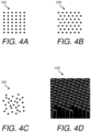
- FIG. 4A shows microposts 122 aligned uniformly in rows and columns
- FIG. 4B shows microposts 122 in staggered or offset rows and/or columns.
- microposts 122 can be positioned randomly but with the density controlled.
- FIG. 4D shows a scanning electron microscope image of an example of an array of microposts 122.
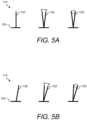
- FIG. 5A and FIG. 5B illustrate sides views of a micropost 122 and show examples of the actuation motion thereof.
- FIG. 5A shows an example of a micropost 122 oriented substantially normal to the plane of substrate 124.
- FIG. 5A shows that the distal end of the micropost 122 can move (1) with side-to-side 2D motion only with respect to the fixed proximal end or (2) with circular motion with respect to the fixed proximal end, which is a cone-shaped motion.
- FIG. 5B shows an example of a micropost 122 oriented at an angle with respect to the plane of substrate 124.
- any fluid in reaction chamber 105 is in effect stirred or caused to flow or circulate within the gap inside reaction chamber 105 and across the surface area thereof.
- FIG. 6, FIG. 7, and FIG. 8 illustrate side views of other examples of the presently disclosed modular active surface devices 100.
- the individual modular active surface device 100 shown is one device only, which has been formed in a large-scale manufacturing process that includes, for example, a wafer that is diced into multiple modular active surface devices 100.
- modular active surface device 100 includes micropost active surface layer 110, as described with reference to FIG. 3A through 5B .
- microposts 122 (not visible in FIG. 6 ) of micropost active surface layer 110 are extending into reaction chamber 105.
- Micropost active surface layer 110 is mounted atop active surface substrate 130.
- Active surface substrate 130 can be a rigid or semi-rigid substrate formed, for example, of glass, plastic, silicon, or silicone.
- active surface substrate 130 is a plastic substrate, such as a substrate formed of the semi-rigid Melinex ® brand polyester film available from DuPont Teijin Films (Chester, VA).
- the thickness of the Melinex ® active surface substrate 130 can be from about 100 ⁇ m to about 500 ⁇ m in one example, or is about 250 ⁇ m in another example. Further, through-holes in micropost active surface layer 110 and active surface substrate 130 form fluid ports 112 (e.g., an input port and output port) in relation to reaction chamber 105.
- fluid ports 112 e.g., an input port and output port
- Some determining characteristics of active surface substrate 130 can include, for example, optical transparency, thickness, rigidity, flexibility, whether passive or active (e.g., electrodes, magnets, LEDs, micropost actuation mechanisms, micropost motion detection mechanisms, etc.), and/or function.
- Function can be, for example, magnetic applications (e.g., generating a magnetic field via embedded wires or coils, magnetic sensors such as a Hall Effect sensors), optical sensor applications, and/or illumination applications.
- micropost active surface layer 110 which is an active surface material such as PDMS
- active surface substrate 130 which is plastic.
- This plasma bonding process has certain advantages over using an adhesive to bond the active surface material micropost active surface layer 110 to the plastic active surface substrate 130. More details of this plasma bonding process are shown and described hereinbelow with reference to FIG. 19 .
- Mask layer 140 that is mounted atop micropost active surface layer 110 can be, for example, a plastic mask.
- the thickness of mask layer 140 can be from about 50 ⁇ m to about 1,000 ⁇ m in one example, or is about 150 ⁇ m in another example.
- openings in mask layer 140 can define certain features of modular active surface devices 100, such as the area, height, and volume of reaction chamber 105. Examples of other features that can be formed using mask layer 140 are shown hereinbelow with reference to FIG. 22A and FIG. 22B .
- modular active surface devices 100 are not limited to one reaction chamber only. Modular active surface devices 100 can includes multiple reaction chambers, an example of which shown hereinbelow with reference to FIG. 23A and FIG. 23B .
- Substrate 150 that is mounted atop mask layer 140 can be, for example, a plastic, glass, or silicon substrate.
- substrate 150 performs two functions (1) to work in combination with micropost active surface layer 110 to form reaction chamber 105 and (2) to protect microposts 122 of micropost active surface layer 110 when modular active surface device 100 is handled.
- substrate 150 is formed of polyethylene terephthalate (PET).
- PET polyethylene terephthalate
- the thickness of the PET substrate 150 can be from about 100 ⁇ m to about 500 ⁇ m in one example, or is about 380 ⁇ m (15 mils) in another example.
- substrate 150 can be a microarray.
- a microarray can be, for example, a 2D array of capture elements immobilized on a solid substrate that assays large amounts of biological material using high-throughput screening miniaturized, multiplexed and parallel processing, and detection methods.
- an adhesive layer 142 is provided on one side of mask layer 140 for bonding to micropost active surface layer 110.
- adhesive layer 142 is ARcare 90445, which has a clear peelable liner.
- An adhesive layer 144 is provided on the other side of mask layer 140 for bonding to substrate 150.
- adhesive layer 144 is ARcare 90106, which has a white peelable liner.
- Adhesive layer 142 and adhesive layer 144 are "pressure sensitive" adhesives, meaning they require pressure only (no solvents, heat, UV, etc.) to make the bond.
- mask layer 140 can exist as a single layer of transfer adhesive (i.e., an adhesive layer that is sticky on both top and bottom surfaces).
- each of the protective layers 152 is a liner with an adhesive that adheres strongly to the liner and weakly to modular active surface device 100.
- Protective layers 152 provide a sealed structure when diced from the wafer.
- One or both protective layers 152 can be peeled off for installing modular active surface device 100 into, for example, a receiving fluidics cartridge 200.
- the protective layer 152 on the outer surface of substrate 150 can be peeled away in order to bond the substrate 150-side of modular active surface device 100 to the end user's substrate.
- modular active surface device 100 can have any orientation depending on the end user's system. Namely, modular active surface device 100 can be oriented substrate 150-side up or active surface substrate 130-side up.
- modular active surface device 100 is substantially the same as the modular active surface device 100 shown in FIG. 6 except for the addition of a support layer 160 to provide additional rigidity and strength to the structure.
- support layer 160 is bonded to active surface substrate 130 via another adhesive layer 142 (e.g., ARcare 90445).
- support layer 160 is a thick layer of acrylic, also with the through-holes (i.e., fluid ports 112).
- the thickness of the acrylic support layer 160 can be from about 500 ⁇ m to about 5 mm in one example, or is about 800 ⁇ m (1/32 inches) in another example.
- One function of support layer 160 is to be thick and rigid enough to interface with a pipette without damaging reaction chamber 105. Therefore, the thickness of support layer 160 may be determined by a specific function or purpose.
- the modular active surface devices 100 shown in FIG. 6 and FIG. 7 are examples of devices that include microposts 122 on one surface only of reaction chamber 105.
- the modular active surface device 100 shown in FIG. 8 is an example of a device that includes microposts 122 on both surfaces of reaction chamber 105.
- the modular active surface device 100 shown in FIG. 8 is substantially the same as the modular active surface device 100 shown in FIG. 6 except that substrate 150 is replaced with another instance of micropost active surface layer 110 and active surface substrate 130.
- the two active surface layers 110 face each other on opposite sides of reaction chamber 105.
- a support layer 160 (not shown) can be provided on one or both sides of the modular active surface device 100 shown in FIG. 8 .
- FIG. 9A through FIG. 17 show examples of certain steps of a process of mass producing the presently disclosed modular active surface devices 100 via a wafer-scale manufacturing process. However, more details of a wafer-scale method of mass producing the presently disclosed modular active surface devices 100 is shown and described hereinbelow with reference to FIG. 18 . Further, the process steps shown in FIG. 9A through FIG. 17 are not limited to wafer-scale manufacturing only. The process steps shown in FIG. 9A through FIG. 17 are equally applicable to other manufacturing processes, such as platter-scale manufacturing processes (e.g., using 60-inch glass panels), roll-to-roll laser die cutting processes (e.g., using 10-meter long rolls), and the like.
- platter-scale manufacturing processes e.g., using 60-inch glass panels
- roll-to-roll laser die cutting processes e.g., using 10-meter long rolls
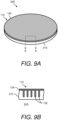
- FIG. 9A shows a perspective view of an example of an active surface material-filled substrate 300 (for example, a PDMS-filled substrate).
- Active surface material-filled substrate 300 includes the active surface material microposts 122 of micropost active surface layer 110 embedded in a substrate 310.
- FIG. 9B shows a cross-sectional view of active surface material-filled substrate 300 taken along line A-A of FIG. 9A .
- substrate 310 provides a template or platform for forming microposts 122 and substrate 124 (see FIG. 3A through FIG. 5B ).
- substrate 310 is a polycarbonate (PC) substrate in which the active surface material microposts 122 are embedded (for example, wherein the active surface material may include, but is not limited to PDMS). Other materials may be used to form flexible microposts 122.
- Active surface material-filled substrate 300 means that the PC substrate 310 is "filled" with the active surface material microposts 122, for example PDMS microposts.
- Substrate 310 is a "sacrificial" substrate that will be removed in subsequent process steps in the fabrication of the modular active surface devices 100.
- Active surface material-filled substrate 300 can be, for example, a 6-inch or 12-inch diameter substrate.
- FIG. 10B show a process of orienting active surface material-filled substrate 300 with substrate 124 of micropost active surface layer 110 facing downward and substrate 310 facing upward.
- FIG. 10C shows a cross-sectional view of active surface material-filled substrate 300 taken along line A-A of FIG. 10B and in the fully oriented position.
- FIG. 11A and FIG. 11B show a process of bonding active surface material-filled substrate 300 to active surface substrate 130 to form an active surface wafer 400.
- the substrate 124-side of active surface material-filled substrate 300 is bonded to active surface substrate 130 using a plasma bonding process, as described hereinbelow with reference to FIG. 19 .
- FIG. 11C shows a cross-sectional view of active surface wafer 400 taken along line A-A of FIG. 11B .
- active surface wafer 400 includes active surface substrate 130, then micropost active surface layer 110 atop active surface substrate 130, then the active surface material microposts 122 of micropost active surface layer 110 embedded in substrate 310.
- Active surface wafer 400 can be, for example, a 6-inch or 12-inch diameter wafer.
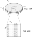
- FIG. 12A and FIG. 12B show active surface wafer 400 with a plurality of fluid ports 112 (i.e., through-holes) cut therein to form a cut active surface wafer 400.
- FIG. 12B shows a plan view of a portion of the cut active surface wafer 400.
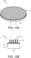
- FIG. 13A and FIG. 13B show a released active surface wafer 500.
- released means that the substrate 310 in which microposts 122 of micropost active surface layer 110 are embedded has been removed. In this way, microposts 122 are freestanding atop active surface substrate 130 and able to be actuated.
- the fluid ports 112 i.e., through-holes
- FIG. 13B shows a cross-sectional view of released active surface wafer 500 taken along line A-A of FIG. 13B .
- Released active surface wafer 500 has a substantially continuous field or array of released (i.e., free-standing) microposts 122 across its area. Released active surface wafer 500 can be, for example, a 6-inch or 12-inch diameter wafer.
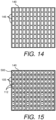
- FIG. 14 shows a plan view an example of mask layer 140 for forming the presently disclosed modular active surface devices 100.
- the portion of mask layer 140 shown in FIG. 14 corresponds to the portion of cut active surface wafer 400 shown in FIG. 12B .
- mask layer 140 has openings 146 arranged in rows and columns, wherein the openings 146 will become the reaction chambers 105 of the respective modular active surface devices 100 when fully formed.
- FIG. 15 shows mask layer 140 atop and in relation to released active surface wafer 500 for forming the presently disclosed modular active surface devices 100.
- the portion of mask layer 140 and released active surface wafer 500 shown in FIG. 15 corresponds to the portion of cut active surface wafer 400 shown in FIG. 12B .
- each opening 146 of mask layer 140 corresponds to the reaction chamber 105 of an eventual modular active surface device 100.
- FIG. 15 shows each opening 146 of mask layer 140 substantially aligned with a pair of fluid ports 112 in released active surface wafer 500.
- Mask layer 140 is adhered (pressure-fitted) to the micropost 122-side of released active surface wafer 500. Because released active surface wafer 500 has a continuous field or array of released microposts 122, the structural members that form mask layer 140 will crush certain microposts 122 atop released active surface wafer 500, leaving intact only those free-standing microposts 122 landing inside openings 146 of mask layer 140.
- FIG. 16 shows certain protective layers added to the released active surface wafer 500 and mask layer 140 structure.
- the portion of wafer structure shown in FIG. 16 corresponds to the portion of cut active surface wafer 400 shown in FIG. 12B .
- the PET substrate 150 and a protective layer 152 are added atop mask layer 140.
- another protective layer 152 is added on the underside of released active surface wafer 500 (e.g., on the outer surface of active surface substrate 130).
- the wafer structure is sealed and ready for dicing into individual modular active surface devices 100.
- FIG. 17 shows the wafer structure diced into multiple individual modular active surface devices 100.
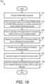
- FIG. 18 illustrates a block diagram of the method 600 of mass producing the presently disclosed modular active surface devices 100, according to the present invention.
- Method 600 supports a wafer-scale manufacturing process for making the presently disclosed modular active surface devices 100.
- the process steps of method 600 are not limited to wafer-scale manufacturing only.
- the process steps of method 600 are equally applicable to other manufacturing processes, such as platter-scale manufacturing processes (e.g., using 60-inch glass panels), roll-to-roll laser die cutting processes (e.g., using 10-meter long rolls), and the like.
- Method 600 includes the following steps.
- a active surface material-filled substrate is provided.
- the active surface material-filled substrate 300 is provided that includes the active surface material microposts 122 of micropost active surface layer 110 embedded in substrate 310 (e.g., a polycarbonate substrate 310).
- the active surface material-filled substrate 300 can be, for example, a 6-inch or 12-inch diameter substrate.
- the active surface wafer 400 is formed by bonding the active surface material-side of the active surface material-filled substrate 300 to another substrate using a plasma bonding process.
- the active surface wafer 400 is formed by bonding the active surface material substrate 124-side of the active surface material-filled substrate to a plastic active surface substrate 130 (e.g., the Melinex ® active surface substrate 130) using the plasma bonding process described hereinbelow with reference to FIG. 19 .
- the active surface wafer 400 can be, for example, a 6-inch or 12-inch diameter wafer.
- a plurality of through-holes are formed in active surface wafer 400 to form a cut active surface wafer 400.
- a plurality of through-holes i.e., fluid ports 112 are formed in active surface wafer 400 using standard etching processes.
- the cut active surface wafer 400 can be, for example, a 6-inch or 12-inch diameter wafer.
- the released active surface wafer 500 is formed by releasing the microposts 122 of the cut active surface wafer 400 as shown, for example, in FIG. 13A and FIG. 13B .
- substrate 310 of the original active surface material-filled substrate 300 (step 610) in which the active surface material microposts 122 are embedded is removed.
- substrate 310 is removed using a solvent, leaving behind the released microposts 122 atop active surface substrate 130, wherein the released microposts 122 are extending outwards away from active surface substrate 130.
- the released active surface wafer 500 is formed.
- the released active surface wafer 500 can be, for example, a 6-inch or 12-inch diameter wafer.
- a mask is provided and installed atop the released active surface wafer 500.
- mask layer 140 provided and installed atop the released active surface wafer 500 with openings 146 positioned in relation to the through-holes (i.e., fluid ports 112) to form the eventual reaction chambers 105.
- both sides of the masked active surface wafer are sealed.
- the PET substrate 150 and then the first protective layer 152 are installed atop mask layer 140, thereby sealing the eventual reaction chambers 105.
- the second protective layer 152 is installed on the underside of released active surface wafer 500 (e.g., on the outside surface of active surface substrate 130), thereby sealing the through-holes which are the eventual fluid ports 112.
- a support layer e.g., support layer 160 shown in FIG. 7
- the second protective layer 152 is installed on the outside surface of the support layer.
- the masked and sealed active surface wafer is diced into multiple individual modular active surface devices 100 using, for example, a laser cutting process, as shown for example, in FIG. 17 .
- the active surface material substrate 124-portion of micropost active surface layer 110 can be bonded to, for example, the plastic (e.g., Melinex ® ) active surface substrate 130 using an adhesive, such as ARclad ® IS-7876.
- an adhesive bond runs risk of failing during the process of releasing microposts 122 in step 625 of method 600 of FIG. 18 and causing the active surface material micropost active surface layer 110 and the plastic active surface substrate 130 to delaminate.
- FIG. 19 shows a block diagram of an example of a method 700 of using a plasma bonding process to bond the micropost array to a substrate. Method 700 may be used, for example, in step 615 of method 600 of FIG. 18 .
- a plasma bonding process is used to bond the active surface material substrate 124-portion of micropost active surface layer 110 to the plastic (e.g., Melinex ® ) active surface substrate 130.
- the benefit of using the plasma bonding process of method 700 is that it mitigates the delamination risk of using an adhesive bond. That is, the plasma bond can tolerate the process of releasing the microposts 122 that is described in step 625 of method 600 of FIG. 18 , whereas an adhesive bond may not.
- Another benefit of the plasma bonding process over using an adhesive is good chemical compatibility.
- Method 700 supports a large-scale manufacturing process for making the presently disclosed modular active surface devices 100. Method 700 may include, but is not limited to, the following steps.
- an active surface material-filled substrate is provided.
- the active surface material-filled substrate 300 is provided that includes the active surface material microposts 122 of micropost active surface layer 110 embedded in substrate 310 (e.g., a polycarbonate substrate 310).
- the active surface material substrate 124 of micropost active surface layer 110 forms one side of the active surface material-filled substrate 300.
- the outer surface of substrate 310 forms the other side of the active surface material-filled substrate 300, wherein substrate 310 is a sacrificial substrate.
- the active surface material-filled substrate 300 can be, for example, a 6-inch or 12-inch diameter substrate.
- a substrate is provided to which the active surface material substrate 124-portion of micropost active surface layer 110 can be bonded.
- the substrate e.g., active surface substrate 130
- the substrate is the semi-rigid Melinex ® brand polyester film available from DuPont Teijin Films (Chester, VA).
- the thickness of the Melinex ® active surface substrate 130 can be from about 100 ⁇ m to about 500 ⁇ m in one example, or is about 250 ⁇ m in another example.
- the substrate e.g., active surface substrate 130
- a thin silicon oxide layer is deposited on one surface of the substrate (e.g., active surface substrate 130) provided in step 715.
- the silicon oxide layer is formed atop the plastic active surface substrate 130 using a plasma-enhanced chemical vapor deposition (PECVD) process.
- PECVD plasma-enhanced chemical vapor deposition
- the silicon oxide layer is about 0.1 ⁇ m thick.
- a thin film of glass is deposited on a plastic substrate.
- a low-temperature PECVD process e.g., from about 30°C to about 70°C is used.
- the silicon oxide layer is plasma-treated.
- the silicon oxide layer on the plastic active surface substrate 130 e.g., the Melinex ® substrate
- the active surface material substrate 124-portion of micropost active surface layer 110 is put into contact with the silicon oxide layer of the active surface substrate 130 (e.g., the Melinex ® substrate).
- a plasma activation process is performed to bond the active surface material substrate 124-portion of micropost active surface layer 110 to the silicon oxide layer of the active surface substrate 130 (e.g., the Melinex ® substrate).
- a modular active surface device 100 can have any x/y dimensions and thickness, and the reaction chamber 105 can be any area, height, and shape.
- the device is shipped to the end user.
- one or both protective layers 152 can be peeled off, thereby exposing at least one surface that can be easily adhered to the end user's fluidics cartridge (e.g., fluidics cartridge 200).
- the presently disclosed modular active surface devices 100 make integrating an active surface, which can be complex, into a low cost fluidics cartridge very easy and inexpensive.
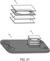
- FIG. 20 and FIG. 21 illustrate perspective views of other examples of the presently disclosed modular active surface devices 100 in relation to corresponding fluidics cartridges 200.
- FIG. 22A and FIG. 22B illustrate plan views showing examples of other features that can be integrated into the presently disclosed modular active surface devices 100.
- mask layer 140 includes opening 146 (for forming reaction chamber 105); an antechamber 114 for receiving, for example, sample fluid; and a fluid path 116 between antechamber 114 and opening 146.
- a quantity of dried reagent 170 is provided within antechamber 114, or along fluid path 116, or both.
- antechamber 114 can be flooded with, for example, sample fluid.
- the modular active surface devices 100 comprise reaction chambers 105 that include multiple antechambers 114.
- multiple antechambers 114 connect to a single fluid path 116 between the multiple antechambers 114 and opening 146.
- the flow of fluids from multiple antechambers 114 into the single fluid path 116 may be controlled by the opening and closing of valves between the multiple antechambers 114 and the single fluid path 116, wherein the opening and closing of the valves are controlled by a control instrument.
- Valving may be implemented in a variety of ways, such as a freeze-thaw valve using a thermoelectric chip, or configuring elastomeric material such as flaps of elastomeric material configured to reduce or eliminate fluid flow in response to positive pressure or a linear actuator.
- an elastomeric film could be utilized, wherein the elastomeric film is configured to reduce or eliminate fluid flow in response to pneumatic or mechanical deflection of the film.
- substrate 150 comprises an elastomeric film configured to reduce or eliminate fluid flow in response to pneumatic or mechanical deflection of the film.
- a dried reagent pellet 175 can be provided in antechamber 114, which can be dissolved (i.e., rehydrated or reconstituted) when sample fluid is added to antechamber 114.
- fluid path 116 has a serpentine path. The purpose of the extended length of the serpentine fluid path 116 is to ensure that there is adequate time for dried reagent pellet 175 to dissolve completely before reaching reaction chamber 105.
- dried reagent 170 and/or dried reagent pellet 175 can be provided in the modular active surface devices 100 at time of manufacture.
- the dried reagent 170 and/or dried reagent pellet 175 are sealed within and stored with modular active surface devices 100 awaiting shipment and use.
- dried reagents using a freeze drying (lyophilization) process, dried reagents and be provided on the microposts 122 themselves.
- one or more of the modular active surface devices 100 comprise reaction chambers 105 that include multiple antechambers 114.
- multiple antechambers 114 connect to a single fluid path 116 between the multiple antechambers 114 and opening 146.
- the flow of fluids from multiple antechambers 114 into the single fluid path 116 may be controlled by the opening and closing of valves between the multiple antechambers 114 and the single fluid path 116, wherein the opening and closing of the valves are controlled by a control instrument.
- valving may be implemented in a variety of ways, such as a freeze-thaw valve using a thermoelectric chip, or configuring elastomeric material such as flaps of elastomeric material configured to reduce or eliminate fluid flow in response to positive pressure or a linear actuator.
- an elastomeric film could be utilized, wherein the elastomeric film is configured to reduce or eliminate fluid flow in response to pneumatic or mechanical deflection of the film.
- substrate 150 comprises an elastomeric film configured to reduce or eliminate fluid flow in response to pneumatic or mechanical deflection of the film.
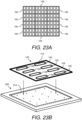
- FIG. 23A and FIG. 23B illustrate an example of the presently disclosed modular active surface devices 100 that have multiple reaction chambers.
- modular active surface device 100 has eight reaction chambers 105, arranged in a 2 x 4 array.
- FIG. 23A shows a plan view of the wafer structure diced into multiple individual modular active surface devices 100, where each of the modular active surface devices 100 includes eight reaction chambers 105.
- FIG. 23B shows an example of one 8-chamber modular active surface device 100 in relation to a corresponding fluidics cartridge 200.
- any surface in reaction chamber 105 including the microposts 122 themselves, can be modified, for example, to promote binding of a target analyte, to promote binding of something to select out for purifying the sample, modified like a microarray, and so on.
- a completed modular active surface device 100 can be delivered to the user and then surface modifications can be performed in the field.
- modular active surface device 100 can be delivered with blister packs. Then, the blister packs are used to release a surface modification chemical and rinsed when surface modification is complete.
- Modular active surface devices 100 can support certain storage requirements.
- modular active surface devices 100 (or at least the reaction chamber 105-portion) can be held under vacuum or in nitrogen (N2).
- Liquid reagents can be provided in modular active surface devices 100 by, for example, flooding reaction chamber 105 after sealing and then, delivered to end user in this state.
- the openings 146 or reaction chambers 105 can be filled with liquid across the wafer, then the wafer is sealed, then diced, then devices shipped.
- Pellet reagents can be used in modular active surface devices 100, as shown, for example, in FIG. 22B .
- the end user drops the pellet into the device at time of use.
- pellets can be dropped into each device across the wafer, then the wafer is sealed, then diced, then devices shipped.
- An antechamber such as antechamber 114 shown in FIG. 22B , allows a lyophilized pellet to be stored in the module without risking physical damage to the active surface.
- the quality and relative bond strengths of adhesives used in modular active surface devices 100 can be varied. For example, want to be able to peel off protective layers 152 without delaminating other layers of the modular active surface devices 100.
- the bond strength of protective layers 152 is weaker than that of adhesives/bonds at other layers.
- the types of adhesives chosen may be based on materials, chemical, and/or specimen compatibility. Further, certain adhesive layers may undergo degasification.
- modular active surface devices 100 can be provided to the end users absent, for example, the Melinex ® active surface substrate 130. Namely, micropost active surface layer 110 absent the Melinex ® active surface substrate 130. Then, the end user performs method 700 to bond micropost active surface layer 110 to their own plastic active surface substrate 130.
Landscapes
- Chemical & Material Sciences (AREA)
- Health & Medical Sciences (AREA)
- General Health & Medical Sciences (AREA)
- Dispersion Chemistry (AREA)
- Analytical Chemistry (AREA)
- Hematology (AREA)
- Clinical Laboratory Science (AREA)
- Chemical Kinetics & Catalysis (AREA)
- Physics & Mathematics (AREA)
- Fluid Mechanics (AREA)
- Molecular Biology (AREA)
- Life Sciences & Earth Sciences (AREA)
- Physical Or Chemical Processes And Apparatus (AREA)
- Micromachines (AREA)
Claims (13)
- Ein Herstellungsprozess im Wafer-Maßstab zum Produzieren einer modularen Vorrichtung mit aktiver Oberfläche, beinhaltend die folgenden Schritte:(a) Bereitstellen eines mit Material mit aktiver Oberfläche gefüllten Substrats, beinhaltend Mikropfosten aus Material mit aktiver Oberfläche der Schicht aus Mikropfosten mit aktiver Oberfläche, die in dem Substrat eingebettet ist;(b) Bilden eines Wafers mit aktiver Oberfläche durch Bonden der Seite mit Material mit aktiver Oberfläche des mit Material mit aktiver Oberfläche gefüllten Substrats an ein zweites Substrat unter Verwendung eines Plasmabondingprozesses;(c) Bilden einer Vielzahl von Durchgangslöchern in dem Wafer mit aktiver Oberfläche, um einen geschnittenen Wafer mit aktiver Oberfläche zu bilden;(d) Freilegen der Mikropfosten des geschnittenen Wafers mit aktiver Oberfläche, um einen Wafer mit freigelegter aktiver Oberfläche zu bilden;(e) Bereitstellen einer Maskenschicht und Installieren der Maskenschicht oben auf dem Wafer mit freigelegter aktiver Oberfläche, um einen Wafer mit maskierter aktiver Oberfläche zu bilden;(f) Versiegeln beider Seiten des Wafers mit maskierter aktiver Oberfläche, um einen Wafer mit maskierter und versiegelter aktiver Oberfläche zu produzieren; und(g) Zerteilen des Wafers mit maskierter und versiegelter aktiver Oberfläche in multiple individuelle modulare Vorrichtungen mit aktiver Oberfläche;wobei jede der modularen Vorrichtungen mit aktiver Oberfläche Folgendes beinhaltet:eine erste aktive Oberfläche oben auf einem ersten Substrat mit aktiver Oberfläche;mindestens eine Reaktionskammer, die Fluidanschlüsse beinhaltet, wobei die Fluidanschlüsse einen oder mehrere Eingangsanschlüsse und einen oder mehrere Ausgangsanschlüsse beinhalten; undeine oder mehrere zusätzliche Schichten, ausgewählt aus der Gruppe, bestehend aus einer oder mehreren Adhesivschichten, einer oder mehreren versteifenden Schichten zum Erleichtern des Handhabens und einer oder mehreren Versiegelungsschichten zum Abziehen;wobei die erste aktive Oberfläche oben auf dem ersten Substrat mit der aktiven Oberfläche mindestens eine Oberfläche der Reaktionskammer bildet; und wobei ferner die modulare Vorrichtung mit aktiver Oberfläche konfiguriert ist, um in eine Mikrofluidikkartusche integriert zu werden.
- Herstellungsprozess im Wafer-Maßstab gemäß Anspruch 1, wobei Schritt (b) ferner die Folgenden Schritte beinhaltet:(b1) Abscheiden einer Siliciumoxidschicht auf eine Oberfläche des zweiten Substrats;(b2) Plasmabehandeln der Siliciumoxidschicht;(b3) Platzieren des Substratabschnitts mit Material mit aktiver Oberfläche des Mikropfostenarrays in Kontakt mit der Siliciumoxidschicht des zweiten Substrats; und(b4) Durchführen eines Plasmaaktivierungsprozesses, um den Substratabschnitt mit Material mit aktiver Oberfläche des Mikropfostenarrays an die Siliciumoxidschicht des Substrats zu bonden.
- Herstellungsprozess im Wafer-Maßstab gemäß Anspruch 1 oder 2, wobei das Material mit aktiver Oberfläche Polydimethylsiloxan (PDMS) ist.
- Herstellungsprozess im Wafer-Maßstab gemäß einem der Ansprüche 1 bis 3, wobei die modulare Vorrichtung mit aktiver Oberfläche ferner Folgendes beinhaltet:eine oben auf der ersten aktiven Oberfläche montierte Maske, wobei die Maske den Bereich, die Höhe und das Volumen der Reaktionskammer definiert,und wahlweise ferner beinhaltend ein zweites oben auf der Maske montiertes Substrat, wobei eine Oberfläche des zweiten Substrats der ersten aktiven Oberfläche zugewandt ist,und wahlweise wobei die Oberfläche des zweiten Substrats, die der ersten aktiven Oberfläche zugewandt ist, eine zweite aktive Oberfläche beinhaltet und wobei ferner die erste aktive Oberfläche und die zweite aktive Oberfläche durch einen Raum getrennt sind.
- Herstellungsprozess im Wafer-Maßstab gemäß einem der Ansprüche 1 bis 4, wobei die aktiven Oberflächen konfiguriert sind, um ein Fluid im Inneren der Reaktionskammer zu manipulieren, wobei Manipulation des Fluids im Inneren der Reaktionskammer ausgewählt ist aus der Gruppe, bestehend aus Erzeugen von Fluidströmung, Verändern des Strömungsprofils eines extern angetriebenen Fluids, Fraktionieren einer Probe in konstituierende Teile, Etablieren eines oder mehrerer Konzentrationsgradienten und Eliminieren eines oder mehrerer Konzentrationsgradienten.
- Herstellungsprozess im Wafer-Maßstab gemäß einem der Ansprüche 1 bis 5, wobei die Substrate mit aktiver Oberfläche starre oder halbstarre Kunststoffsubstrate sind.
- Herstellungsprozess im Wafer-Maßstab gemäß einem der Ansprüche 1 bis 6, wobei die aktiven Oberflächen Schichten mit aktiver Oberfläche mit Mikropfosten sind, beinhaltend oberflächenangebrachte Mikropfosten, wahlweise wobei die oberflächenangebrachten Mikropfosten in Arrays angeordnet sind und wahlweise wobei die oberflächenangebrachten Mikropfosten zur Betätigung in Gegenwart einer Betätigungskraft konfiguriert sind, wobei die Betätigungskraft die beweglichen, oberflächenangebrachten Mikropfosten in Bewegung betätigen und wahlweise wobei die Betätigungskraft ausgewählt ist aus der Gruppe, bestehend aus einem Magnetfeld, einem Wärmefeld, einem Schallfeld, einem elektrischen Feld und einem Schwingungsfeld.
- Herstellungsprozess im Wafer-Maßstab gemäß einem der Ansprüche 1 bis 7, wobei die aktiven Oberflächen mit Mikropfosten in der Reaktionskammer für Mischvorgänge, Bindevorgänge und Zellverarbeitungsvorgänge konfiguriert sind, wahlweise wobei die Zellverarbeitungsvorgänge ausgewählt sind aus der Gruppe, bestehend aus Zellkonzentrierung, Zellsammlung, Zellfiltration, Zellenwaschung, Zellenzählen, Zellenrückgewinnung, Zellenlyse und Zellentklumpen.
- Herstellungsprozess im Wafer-Maßstab gemäß einem der Ansprüche 1 bis 8, wobei die modulare Vorrichtung mit aktiver Oberfläche konfiguriert ist, um in eine vertiefte Region einer Mikrofluidikkartusche integriert zu werden, wahlweise wobei die Mikrofluidikkartusche ferner Fluidleitungen beinhaltet, die eingerichtet sind, um dem Fluidanschluss zu entsprechen, wobei, wenn die Mikrofluidikkartusche die modulare Vorrichtung mit aktiver Oberfläche aufnimmt, wobei die Mikrofluidikkartusche und die modulare Vorrichtung mit aktiver Oberfläche fluidisch gekoppelt sind.
- Herstellungsprozess im Wafer-Maßstab gemäß einem der Ansprüche 1 bis 9, wobei die modulare Vorrichtung mit aktiver Oberfläche ferner eine Adhesivschicht zum Bonden an die Mikrofluidikkartusche beinhaltet.
- Herstellungsprozess im Wafer-Maßstab gemäß einem der Ansprüche 7 bis 10, wobei die Mikropfosten aus einem Material mit aktiver Oberfläche gebildet sind, wahlweise wobei das Material mit aktiver Oberfläche Polydimethylsiloxan (PDMS) ist; und/oderwobei die Mikropfosten in der Länge von etwa 1 µm bis etwa 100 µm reichen; und/oder wobei die Mikropfosten im Durchmesser von etwa 0,1 µm bis etwa 10 µm reichen; und/oderwobei die Mikropfosten eine Querschnittsform aufweisen, ausgewählt aus der Gruppe, bestehend aus kreisförmig, oval, quadratisch, rechteckig und dreieckig; und/oderwobei die Mikropfosten im Wesentlichen normal zu der Ebene des Substrats orientiert sind oder wobei die Mikropfosten bei einem Winkel α bezüglich der Normalen der Ebene des Substrats orientiert sind; und/oder wobei die Mikropfosten bei einer Steigung von etwa 0 µm bis etwa 50 µm orientiert sind.
- Herstellungsprozess im Wafer-Maßstab gemäß einem der Ansprüche 7 bis 11, wobei die Maskenschicht eine Öffnung zum Bilden der Reaktionskammer, einer Vorkammer und eines Fluidpfads zwischen der Vorkammer und der Öffnung beinhaltet, wahlweise wobei die Vorkammer getrocknetes Reagenz und/oder ein getrocknetes Reagenzpellet beinhaltet, die konfiguriert sind, um sich aufzulösen, wenn ein Probenfluid zu der Vorkammer hinzugefügt wird, wodurch einer Mischung aus Probenfluid und Reagenz ermöglicht wird, in die Reaktionskammer zu strömen, und wahlweise wobei der Fluidpfad einen Serpentinenpfad aufweist, der konfiguriert ist, um adäquate Zeit für das getrocknete Reagenz und/oder getrocknete Reagenzpellet bereitzustellen, um sich vollständig aufzulösen, bevor die Reaktionskammer erreicht wird.
- Herstellungsprozess im Wafer-Maßstab gemäß Anspruch 12, wobei die modulare Vorrichtung mit aktiver Oberfläche Folgendes beinhaltet:(i) multiple Vorkammern und separate Fluidpfade zwischen jeder Vorkammer und Öffnung; oder(ii) multiple Vorkammern und einen einzelnen Fluidpfad zwischen den multiplen Vorkammern und der Öffnung, wahlweise wobei die Strömung von Fluiden aus den multiplen Vorkammern in den einzelnen Fluidpfad durch das Öffnen und Schließen von Ventilen zwischen den multiplen Vorkammern und dem einzelnen Fluidpfad gesteuert wird und wobei das Öffnen und Schließen der Ventile durch ein Steuerungsinstrument gesteuert werden.
Priority Applications (1)
| Application Number | Priority Date | Filing Date | Title |
|---|---|---|---|
| EP24191597.4A EP4484011A3 (de) | 2017-06-20 | 2018-06-19 | Modulare aktive oberflächenvorrichtungen für mikrofluidische systeme und verfahren zur herstellung davon |
Applications Claiming Priority (3)
| Application Number | Priority Date | Filing Date | Title |
|---|---|---|---|
| US201762522536P | 2017-06-20 | 2017-06-20 | |
| PCT/US2018/038234 WO2018236833A1 (en) | 2017-06-20 | 2018-06-19 | Modular active surface devices for microfluidic systems and methods of making same |
| EP18821168.4A EP3645164A4 (de) | 2017-06-20 | 2018-06-19 | Modulare aktive oberflächenvorrichtungen für mikrofluidische systeme und verfahren zu deren herstellung |
Related Parent Applications (1)
| Application Number | Title | Priority Date | Filing Date |
|---|---|---|---|
| EP18821168.4A Division EP3645164A4 (de) | 2017-06-20 | 2018-06-19 | Modulare aktive oberflächenvorrichtungen für mikrofluidische systeme und verfahren zu deren herstellung |
Related Child Applications (1)
| Application Number | Title | Priority Date | Filing Date |
|---|---|---|---|
| EP24191597.4A Division EP4484011A3 (de) | 2017-06-20 | 2018-06-19 | Modulare aktive oberflächenvorrichtungen für mikrofluidische systeme und verfahren zur herstellung davon |
Publications (2)
| Publication Number | Publication Date |
|---|---|
| EP4005675A1 EP4005675A1 (de) | 2022-06-01 |
| EP4005675B1 true EP4005675B1 (de) | 2024-07-31 |
Family
ID=64737804
Family Applications (3)
| Application Number | Title | Priority Date | Filing Date |
|---|---|---|---|
| EP22151888.9A Active EP4005675B1 (de) | 2017-06-20 | 2018-06-19 | Verfahren zum herstellen von modularen vorrichtungen mit aktiver oberfläche fürmikrofluidische systeme |
| EP18821168.4A Withdrawn EP3645164A4 (de) | 2017-06-20 | 2018-06-19 | Modulare aktive oberflächenvorrichtungen für mikrofluidische systeme und verfahren zu deren herstellung |
| EP24191597.4A Pending EP4484011A3 (de) | 2017-06-20 | 2018-06-19 | Modulare aktive oberflächenvorrichtungen für mikrofluidische systeme und verfahren zur herstellung davon |
Family Applications After (2)
| Application Number | Title | Priority Date | Filing Date |
|---|---|---|---|
| EP18821168.4A Withdrawn EP3645164A4 (de) | 2017-06-20 | 2018-06-19 | Modulare aktive oberflächenvorrichtungen für mikrofluidische systeme und verfahren zu deren herstellung |
| EP24191597.4A Pending EP4484011A3 (de) | 2017-06-20 | 2018-06-19 | Modulare aktive oberflächenvorrichtungen für mikrofluidische systeme und verfahren zur herstellung davon |
Country Status (4)
| Country | Link |
|---|---|
| US (2) | US11571694B2 (de) |
| EP (3) | EP4005675B1 (de) |
| AU (1) | AU2018289391B2 (de) |
| WO (1) | WO2018236833A1 (de) |
Families Citing this family (13)
| Publication number | Priority date | Publication date | Assignee | Title |
|---|---|---|---|---|
| WO2021087449A1 (en) * | 2019-11-01 | 2021-05-06 | Redbud Labs, Inc. | Active surface devices for and methods of providing dried reagents in microfluidic applications |
| EP4005675B1 (de) * | 2017-06-20 | 2024-07-31 | Redbud Labs, Inc. | Verfahren zum herstellen von modularen vorrichtungen mit aktiver oberfläche fürmikrofluidische systeme |
| WO2020190462A1 (en) * | 2019-03-18 | 2020-09-24 | Siemens Healthcare Diagnostics Inc. | Diagnostic consumables incorporating coated micro-projection arrays, and methods thereof |
| WO2020261086A1 (en) * | 2019-06-28 | 2020-12-30 | 3M Innovative Properties Company | Articles having conformal layers and methods of making same |
| CN114269476A (zh) * | 2019-08-21 | 2022-04-01 | 隆萨沃克斯维尔股份有限公司 | 带混合区的内毒素检测用筒体 |
| EP4100738A4 (de) * | 2020-02-07 | 2024-03-06 | National Research Council of Canada | Mikrofluidische vorrichtung mit einer schnittstelle, die reaktionsgefässe in einer durchflusskammer fixiert, kit zum bilden und verwendung derselben |
| US20210252508A1 (en) * | 2020-02-15 | 2021-08-19 | Heska Corporation | Sample cartridges |
| EP4178720A4 (de) * | 2020-07-07 | 2025-05-07 | Redbud Labs, Inc. | Bioreaktorsystem im mikromassstab und verfahren zur bereitstellung von zellkulturwachstumsbedingungen in einem kleinvolumigen gefäss |
| WO2022046715A1 (en) * | 2020-08-26 | 2022-03-03 | Redbud Labs, Inc. | Modular active surface devices for microfluidic systems and methods of making same including adhesive-free assembly |
| USD963724S1 (en) * | 2020-09-02 | 2022-09-13 | Mikroscan Technologies | Slide holder |
| GB202109635D0 (en) * | 2021-07-02 | 2021-08-18 | Randox Laboratories Ltd | Vision system |
| IL310749A (en) * | 2021-08-12 | 2024-04-01 | Coagulo Medical Tech Inc | Modular multilayer microfluidic cartridges |
| DE102024202356A1 (de) * | 2024-03-13 | 2025-09-18 | Robert Bosch Gesellschaft mit beschränkter Haftung | Modulares System für eine mikrofluidische Kartusche, insbesondere zur Analyse einer biologischen Probe |
Family Cites Families (11)
| Publication number | Priority date | Publication date | Assignee | Title |
|---|---|---|---|---|
| GB0327094D0 (en) * | 2003-11-21 | 2003-12-24 | Inverness Medical Switzerland | Laminated device |
| US7919062B2 (en) * | 2008-03-20 | 2011-04-05 | Corning Incorporated | Modular microfluidic system and method for building a modular microfludic system |
| CA2731413A1 (en) | 2008-07-21 | 2010-01-28 | Valorbec S.E.C. | A microfluidic device and method for fabricating the microfluidic device |
| US8586368B2 (en) * | 2009-06-25 | 2013-11-19 | The University Of North Carolina At Chapel Hill | Methods and systems for using actuated surface-attached posts for assessing biofluid rheology |
| US20110104817A1 (en) * | 2009-10-20 | 2011-05-05 | Science, Technology And Research | Integrated micro device, a method for detecting biomarkers using the integrated micro device, a method for manufacturing an integrated micro device, and an integrated micro device arrangement |
| US9700889B2 (en) * | 2009-11-23 | 2017-07-11 | Cyvek, Inc. | Methods and systems for manufacture of microarray assay systems, conducting microfluidic assays, and monitoring and scanning to obtain microfluidic assay results |
| EP2814942B1 (de) | 2012-02-13 | 2024-07-03 | Neumodx Molecular, Inc. | Mikrofluidische kartusche zur verarbeitung und zum nachweis von nucleinsäuren |
| KR20170016915A (ko) | 2014-06-11 | 2017-02-14 | 마이크로닉스 인코포레이티드. | 핵산의 분석을 위한 통합 검정 대조군을 갖는 마이크로 유체 공학적 카트리지 및 장치 |
| WO2016136273A1 (ja) * | 2015-02-27 | 2016-09-01 | 凸版印刷株式会社 | 細胞を分離する方法、およびそのためのデバイス |
| AU2016324467B2 (en) * | 2015-09-18 | 2021-12-02 | Redbud Labs, Inc. | Flow cells utilizing surface-attached structures, and related systems and methods |
| EP4005675B1 (de) * | 2017-06-20 | 2024-07-31 | Redbud Labs, Inc. | Verfahren zum herstellen von modularen vorrichtungen mit aktiver oberfläche fürmikrofluidische systeme |
-
2018
- 2018-06-19 EP EP22151888.9A patent/EP4005675B1/de active Active
- 2018-06-19 EP EP18821168.4A patent/EP3645164A4/de not_active Withdrawn
- 2018-06-19 EP EP24191597.4A patent/EP4484011A3/de active Pending
- 2018-06-19 AU AU2018289391A patent/AU2018289391B2/en active Active
- 2018-06-19 WO PCT/US2018/038234 patent/WO2018236833A1/en not_active Ceased
- 2018-06-19 US US16/756,234 patent/US11571694B2/en active Active
-
2022
- 2022-12-28 US US18/147,241 patent/US12303895B2/en active Active
Also Published As
| Publication number | Publication date |
|---|---|
| AU2018289391A1 (en) | 2020-05-21 |
| WO2018236833A1 (en) | 2018-12-27 |
| EP4484011A2 (de) | 2025-01-01 |
| US11571694B2 (en) | 2023-02-07 |
| AU2018289391B2 (en) | 2023-07-20 |
| US20230166254A1 (en) | 2023-06-01 |
| EP4005675A1 (de) | 2022-06-01 |
| US12303895B2 (en) | 2025-05-20 |
| EP3645164A4 (de) | 2021-08-04 |
| EP4484011A3 (de) | 2025-03-12 |
| US20200254454A1 (en) | 2020-08-13 |
| EP3645164A1 (de) | 2020-05-06 |
| CA3074265A1 (en) | 2018-12-27 |
Similar Documents
| Publication | Publication Date | Title |
|---|---|---|
| US12303895B2 (en) | Modular active surface devices for microfluidic systems and methods of making same | |
| US20250041860A1 (en) | Microfluidic Chips and Cartridges and Systems Utilizing Microfluidic Chips and Cartridges | |
| Oh et al. | A review of microvalves | |
| CN106552682B (zh) | 微流体装置以及制造方法和用途 | |
| US8137624B2 (en) | Method and apparatus for attaching a fluid cell to a planar substrate | |
| US20170001194A1 (en) | Microfluidic device, system, and method | |
| CN102298069B (zh) | 用于微型化流体输送及分析系统的一致性阀操作的阀结构 | |
| CN102439692A (zh) | 微流控装置与宏流控装置的接口装置及方法 | |
| JP5948248B2 (ja) | マイクロチップ、及び、マイクロチップの製造方法 | |
| WO2011138676A2 (en) | Integrated microfluidic sensor system with magnetostrictive resonators | |
| JP2004000163A (ja) | 細胞の処理に用いるセル | |
| AU2020373075A1 (en) | Active surface devices for and methods of providing dried reagents in microfluidic applications | |
| US20250161941A1 (en) | Modular Active Surface Devices for Microfluidic Systems and Methods of Making Same | |
| US20080069732A1 (en) | Diagnostic test system | |
| HK40068765A (en) | Methods of making modular active surface devices for microfluidic systems | |
| Chartier et al. | Fabrication of hybrid plastic-silicon microfluidic devices for individual cell manipulation by dielectrophoresis | |
| US20220146510A1 (en) | Methods of surface modification of silicones for specific target and high efficiency binding | |
| US20230226549A1 (en) | Modular Active Surface Devices for Microfluidic Systems and Methods of Making Same Including Adhesive-Free Assembly | |
| Tamanaha et al. | Reusable, compression-sealed fluid cells for surface mounting to planar substrates | |
| US20170261493A1 (en) | Cell culture interfaces, systems, and uses thereof | |
| Tan et al. | Integration of PDMS and PMMA for batch fabrication of microfluidic devices | |
| Tondra et al. | Microfluidic package design for magnetoresistive biosensors | |
| Dharmatilleke et al. | A Hybrid Microfluidic Mini System Towards a “Lab-on-a-Chip” for Biochemical Immunoassay | |
| JP2008032414A (ja) | マイクロチップ |
Legal Events
| Date | Code | Title | Description |
|---|---|---|---|
| PUAI | Public reference made under article 153(3) epc to a published international application that has entered the european phase |
Free format text: ORIGINAL CODE: 0009012 |
|
| STAA | Information on the status of an ep patent application or granted ep patent |
Free format text: STATUS: THE APPLICATION HAS BEEN PUBLISHED |
|
| AC | Divisional application: reference to earlier application |
Ref document number: 3645164 Country of ref document: EP Kind code of ref document: P |
|
| AK | Designated contracting states |
Kind code of ref document: A1 Designated state(s): AL AT BE BG CH CY CZ DE DK EE ES FI FR GB GR HR HU IE IS IT LI LT LU LV MC MK MT NL NO PL PT RO RS SE SI SK SM TR |
|
| REG | Reference to a national code |
Ref country code: HK Ref legal event code: DE Ref document number: 40068765 Country of ref document: HK |
|
| STAA | Information on the status of an ep patent application or granted ep patent |
Free format text: STATUS: REQUEST FOR EXAMINATION WAS MADE |
|
| 17P | Request for examination filed |
Effective date: 20221201 |
|
| RBV | Designated contracting states (corrected) |
Designated state(s): AL AT BE BG CH CY CZ DE DK EE ES FI FR GB GR HR HU IE IS IT LI LT LU LV MC MK MT NL NO PL PT RO RS SE SI SK SM TR |
|
| GRAP | Despatch of communication of intention to grant a patent |
Free format text: ORIGINAL CODE: EPIDOSNIGR1 |
|
| STAA | Information on the status of an ep patent application or granted ep patent |
Free format text: STATUS: GRANT OF PATENT IS INTENDED |
|
| INTG | Intention to grant announced |
Effective date: 20240208 |
|
| GRAS | Grant fee paid |
Free format text: ORIGINAL CODE: EPIDOSNIGR3 |
|
| GRAA | (expected) grant |
Free format text: ORIGINAL CODE: 0009210 |
|
| STAA | Information on the status of an ep patent application or granted ep patent |
Free format text: STATUS: THE PATENT HAS BEEN GRANTED |
|
| RAP3 | Party data changed (applicant data changed or rights of an application transferred) |
Owner name: THE UNIVERSITY OF NORTH CAROLINA AT CHAPEL HILL Owner name: REDBUD LABS, INC. |
|
| AC | Divisional application: reference to earlier application |
Ref document number: 3645164 Country of ref document: EP Kind code of ref document: P |
|
| AK | Designated contracting states |
Kind code of ref document: B1 Designated state(s): AL AT BE BG CH CY CZ DE DK EE ES FI FR GB GR HR HU IE IS IT LI LT LU LV MC MK MT NL NO PL PT RO RS SE SI SK SM TR |
|
| REG | Reference to a national code |
Ref country code: CH Ref legal event code: EP Ref country code: GB Ref legal event code: FG4D |
|
| REG | Reference to a national code |
Ref country code: DE Ref legal event code: R096 Ref document number: 602018072647 Country of ref document: DE |
|
| REG | Reference to a national code |
Ref country code: IE Ref legal event code: FG4D |
|
| P01 | Opt-out of the competence of the unified patent court (upc) registered |
Free format text: CASE NUMBER: UPC_APP_326230/2023 Effective date: 20230523 |
|
| REG | Reference to a national code |
Ref country code: LT Ref legal event code: MG9D |
|
| REG | Reference to a national code |
Ref country code: NL Ref legal event code: MP Effective date: 20240731 |
|
| PG25 | Lapsed in a contracting state [announced via postgrant information from national office to epo] |
Ref country code: PT Free format text: LAPSE BECAUSE OF FAILURE TO SUBMIT A TRANSLATION OF THE DESCRIPTION OR TO PAY THE FEE WITHIN THE PRESCRIBED TIME-LIMIT Effective date: 20241202 |
|
| REG | Reference to a national code |
Ref country code: AT Ref legal event code: MK05 Ref document number: 1707975 Country of ref document: AT Kind code of ref document: T Effective date: 20240731 |
|
| PG25 | Lapsed in a contracting state [announced via postgrant information from national office to epo] |
Ref country code: PT Free format text: LAPSE BECAUSE OF FAILURE TO SUBMIT A TRANSLATION OF THE DESCRIPTION OR TO PAY THE FEE WITHIN THE PRESCRIBED TIME-LIMIT Effective date: 20241202 |
|
| PG25 | Lapsed in a contracting state [announced via postgrant information from national office to epo] |
Ref country code: NO Free format text: LAPSE BECAUSE OF FAILURE TO SUBMIT A TRANSLATION OF THE DESCRIPTION OR TO PAY THE FEE WITHIN THE PRESCRIBED TIME-LIMIT Effective date: 20241031 |
|
| PG25 | Lapsed in a contracting state [announced via postgrant information from national office to epo] |
Ref country code: NL Free format text: LAPSE BECAUSE OF FAILURE TO SUBMIT A TRANSLATION OF THE DESCRIPTION OR TO PAY THE FEE WITHIN THE PRESCRIBED TIME-LIMIT Effective date: 20240731 Ref country code: FI Free format text: LAPSE BECAUSE OF FAILURE TO SUBMIT A TRANSLATION OF THE DESCRIPTION OR TO PAY THE FEE WITHIN THE PRESCRIBED TIME-LIMIT Effective date: 20240731 Ref country code: PL Free format text: LAPSE BECAUSE OF FAILURE TO SUBMIT A TRANSLATION OF THE DESCRIPTION OR TO PAY THE FEE WITHIN THE PRESCRIBED TIME-LIMIT Effective date: 20240731 Ref country code: GR Free format text: LAPSE BECAUSE OF FAILURE TO SUBMIT A TRANSLATION OF THE DESCRIPTION OR TO PAY THE FEE WITHIN THE PRESCRIBED TIME-LIMIT Effective date: 20241101 |
|
| PG25 | Lapsed in a contracting state [announced via postgrant information from national office to epo] |
Ref country code: BG Free format text: LAPSE BECAUSE OF FAILURE TO SUBMIT A TRANSLATION OF THE DESCRIPTION OR TO PAY THE FEE WITHIN THE PRESCRIBED TIME-LIMIT Effective date: 20240731 |
|
| PG25 | Lapsed in a contracting state [announced via postgrant information from national office to epo] |
Ref country code: LV Free format text: LAPSE BECAUSE OF FAILURE TO SUBMIT A TRANSLATION OF THE DESCRIPTION OR TO PAY THE FEE WITHIN THE PRESCRIBED TIME-LIMIT Effective date: 20240731 |
|
| PG25 | Lapsed in a contracting state [announced via postgrant information from national office to epo] |
Ref country code: AT Free format text: LAPSE BECAUSE OF FAILURE TO SUBMIT A TRANSLATION OF THE DESCRIPTION OR TO PAY THE FEE WITHIN THE PRESCRIBED TIME-LIMIT Effective date: 20240731 Ref country code: IS Free format text: LAPSE BECAUSE OF FAILURE TO SUBMIT A TRANSLATION OF THE DESCRIPTION OR TO PAY THE FEE WITHIN THE PRESCRIBED TIME-LIMIT Effective date: 20241130 |
|
| PG25 | Lapsed in a contracting state [announced via postgrant information from national office to epo] |
Ref country code: HR Free format text: LAPSE BECAUSE OF FAILURE TO SUBMIT A TRANSLATION OF THE DESCRIPTION OR TO PAY THE FEE WITHIN THE PRESCRIBED TIME-LIMIT Effective date: 20240731 |
|
| PG25 | Lapsed in a contracting state [announced via postgrant information from national office to epo] |
Ref country code: ES Free format text: LAPSE BECAUSE OF FAILURE TO SUBMIT A TRANSLATION OF THE DESCRIPTION OR TO PAY THE FEE WITHIN THE PRESCRIBED TIME-LIMIT Effective date: 20240731 Ref country code: RS Free format text: LAPSE BECAUSE OF FAILURE TO SUBMIT A TRANSLATION OF THE DESCRIPTION OR TO PAY THE FEE WITHIN THE PRESCRIBED TIME-LIMIT Effective date: 20241031 |
|
| PG25 | Lapsed in a contracting state [announced via postgrant information from national office to epo] |
Ref country code: RS Free format text: LAPSE BECAUSE OF FAILURE TO SUBMIT A TRANSLATION OF THE DESCRIPTION OR TO PAY THE FEE WITHIN THE PRESCRIBED TIME-LIMIT Effective date: 20241031 Ref country code: PL Free format text: LAPSE BECAUSE OF FAILURE TO SUBMIT A TRANSLATION OF THE DESCRIPTION OR TO PAY THE FEE WITHIN THE PRESCRIBED TIME-LIMIT Effective date: 20240731 Ref country code: NO Free format text: LAPSE BECAUSE OF FAILURE TO SUBMIT A TRANSLATION OF THE DESCRIPTION OR TO PAY THE FEE WITHIN THE PRESCRIBED TIME-LIMIT Effective date: 20241031 Ref country code: NL Free format text: LAPSE BECAUSE OF FAILURE TO SUBMIT A TRANSLATION OF THE DESCRIPTION OR TO PAY THE FEE WITHIN THE PRESCRIBED TIME-LIMIT Effective date: 20240731 Ref country code: LV Free format text: LAPSE BECAUSE OF FAILURE TO SUBMIT A TRANSLATION OF THE DESCRIPTION OR TO PAY THE FEE WITHIN THE PRESCRIBED TIME-LIMIT Effective date: 20240731 Ref country code: IS Free format text: LAPSE BECAUSE OF FAILURE TO SUBMIT A TRANSLATION OF THE DESCRIPTION OR TO PAY THE FEE WITHIN THE PRESCRIBED TIME-LIMIT Effective date: 20241130 Ref country code: HR Free format text: LAPSE BECAUSE OF FAILURE TO SUBMIT A TRANSLATION OF THE DESCRIPTION OR TO PAY THE FEE WITHIN THE PRESCRIBED TIME-LIMIT Effective date: 20240731 Ref country code: GR Free format text: LAPSE BECAUSE OF FAILURE TO SUBMIT A TRANSLATION OF THE DESCRIPTION OR TO PAY THE FEE WITHIN THE PRESCRIBED TIME-LIMIT Effective date: 20241101 Ref country code: FI Free format text: LAPSE BECAUSE OF FAILURE TO SUBMIT A TRANSLATION OF THE DESCRIPTION OR TO PAY THE FEE WITHIN THE PRESCRIBED TIME-LIMIT Effective date: 20240731 Ref country code: ES Free format text: LAPSE BECAUSE OF FAILURE TO SUBMIT A TRANSLATION OF THE DESCRIPTION OR TO PAY THE FEE WITHIN THE PRESCRIBED TIME-LIMIT Effective date: 20240731 Ref country code: BG Free format text: LAPSE BECAUSE OF FAILURE TO SUBMIT A TRANSLATION OF THE DESCRIPTION OR TO PAY THE FEE WITHIN THE PRESCRIBED TIME-LIMIT Effective date: 20240731 Ref country code: AT Free format text: LAPSE BECAUSE OF FAILURE TO SUBMIT A TRANSLATION OF THE DESCRIPTION OR TO PAY THE FEE WITHIN THE PRESCRIBED TIME-LIMIT Effective date: 20240731 |
|
| PG25 | Lapsed in a contracting state [announced via postgrant information from national office to epo] |
Ref country code: RO Free format text: LAPSE BECAUSE OF FAILURE TO SUBMIT A TRANSLATION OF THE DESCRIPTION OR TO PAY THE FEE WITHIN THE PRESCRIBED TIME-LIMIT Effective date: 20240731 Ref country code: SM Free format text: LAPSE BECAUSE OF FAILURE TO SUBMIT A TRANSLATION OF THE DESCRIPTION OR TO PAY THE FEE WITHIN THE PRESCRIBED TIME-LIMIT Effective date: 20240731 Ref country code: DK Free format text: LAPSE BECAUSE OF FAILURE TO SUBMIT A TRANSLATION OF THE DESCRIPTION OR TO PAY THE FEE WITHIN THE PRESCRIBED TIME-LIMIT Effective date: 20240731 |
|
| PG25 | Lapsed in a contracting state [announced via postgrant information from national office to epo] |
Ref country code: EE Free format text: LAPSE BECAUSE OF FAILURE TO SUBMIT A TRANSLATION OF THE DESCRIPTION OR TO PAY THE FEE WITHIN THE PRESCRIBED TIME-LIMIT Effective date: 20240731 |
|
| PG25 | Lapsed in a contracting state [announced via postgrant information from national office to epo] |
Ref country code: CZ Free format text: LAPSE BECAUSE OF FAILURE TO SUBMIT A TRANSLATION OF THE DESCRIPTION OR TO PAY THE FEE WITHIN THE PRESCRIBED TIME-LIMIT Effective date: 20240731 |
|
| PG25 | Lapsed in a contracting state [announced via postgrant information from national office to epo] |
Ref country code: SK Free format text: LAPSE BECAUSE OF FAILURE TO SUBMIT A TRANSLATION OF THE DESCRIPTION OR TO PAY THE FEE WITHIN THE PRESCRIBED TIME-LIMIT Effective date: 20240731 Ref country code: IT Free format text: LAPSE BECAUSE OF FAILURE TO SUBMIT A TRANSLATION OF THE DESCRIPTION OR TO PAY THE FEE WITHIN THE PRESCRIBED TIME-LIMIT Effective date: 20240731 |
|
| REG | Reference to a national code |
Ref country code: DE Ref legal event code: R097 Ref document number: 602018072647 Country of ref document: DE |
|
| PLBE | No opposition filed within time limit |
Free format text: ORIGINAL CODE: 0009261 |
|
| STAA | Information on the status of an ep patent application or granted ep patent |
Free format text: STATUS: NO OPPOSITION FILED WITHIN TIME LIMIT |
|
| 26N | No opposition filed |
Effective date: 20250501 |
|
| PG25 | Lapsed in a contracting state [announced via postgrant information from national office to epo] |
Ref country code: SE Free format text: LAPSE BECAUSE OF FAILURE TO SUBMIT A TRANSLATION OF THE DESCRIPTION OR TO PAY THE FEE WITHIN THE PRESCRIBED TIME-LIMIT Effective date: 20240731 |
|
| PGFP | Annual fee paid to national office [announced via postgrant information from national office to epo] |
Ref country code: CH Payment date: 20250701 Year of fee payment: 8 |
|
| PG25 | Lapsed in a contracting state [announced via postgrant information from national office to epo] |
Ref country code: MC Free format text: LAPSE BECAUSE OF FAILURE TO SUBMIT A TRANSLATION OF THE DESCRIPTION OR TO PAY THE FEE WITHIN THE PRESCRIBED TIME-LIMIT Effective date: 20240731 |
|
| PG25 | Lapsed in a contracting state [announced via postgrant information from national office to epo] |
Ref country code: LU Free format text: LAPSE BECAUSE OF NON-PAYMENT OF DUE FEES Effective date: 20250619 |
|
| REG | Reference to a national code |
Ref country code: BE Ref legal event code: MM Effective date: 20250630 |
|
| PG25 | Lapsed in a contracting state [announced via postgrant information from national office to epo] |
Ref country code: IE Free format text: LAPSE BECAUSE OF NON-PAYMENT OF DUE FEES Effective date: 20250619 |
|
| PG25 | Lapsed in a contracting state [announced via postgrant information from national office to epo] |
Ref country code: BE Free format text: LAPSE BECAUSE OF NON-PAYMENT OF DUE FEES Effective date: 20250630 |
|
| PG25 | Lapsed in a contracting state [announced via postgrant information from national office to epo] |
Ref country code: LT Free format text: LAPSE BECAUSE OF FAILURE TO SUBMIT A TRANSLATION OF THE DESCRIPTION OR TO PAY THE FEE WITHIN THE PRESCRIBED TIME-LIMIT Effective date: 20240731 |
|
| REG | Reference to a national code |
Ref country code: CH Ref legal event code: U11 Free format text: ST27 STATUS EVENT CODE: U-0-0-U10-U11 (AS PROVIDED BY THE NATIONAL OFFICE) Effective date: 20260701 |
|
| PGFP | Annual fee paid to national office [announced via postgrant information from national office to epo] |
Ref country code: GB Payment date: 20260622 Year of fee payment: 9 |
|
| PGFP | Annual fee paid to national office [announced via postgrant information from national office to epo] |
Ref country code: DE Payment date: 20260616 Year of fee payment: 9 |
|
| PGFP | Annual fee paid to national office [announced via postgrant information from national office to epo] |
Ref country code: FR Payment date: 20260629 Year of fee payment: 9 |
|
| PG25 | Lapsed in a contracting state [announced via postgrant information from national office to epo] |
Ref country code: CY Free format text: LAPSE BECAUSE OF FAILURE TO SUBMIT A TRANSLATION OF THE DESCRIPTION OR TO PAY THE FEE WITHIN THE PRESCRIBED TIME-LIMIT Effective date: 20240731 |