EP4005116B1 - Drahtloses telekommunikationsnetzwerk - Google Patents
Drahtloses telekommunikationsnetzwerk Download PDFInfo
- Publication number
- EP4005116B1 EP4005116B1 EP20765052.4A EP20765052A EP4005116B1 EP 4005116 B1 EP4005116 B1 EP 4005116B1 EP 20765052 A EP20765052 A EP 20765052A EP 4005116 B1 EP4005116 B1 EP 4005116B1
- Authority
- EP
- European Patent Office
- Prior art keywords
- waveguide
- segment
- variable transparency
- segments
- calibration
- Prior art date
- Legal status (The legal status is an assumption and is not a legal conclusion. Google has not performed a legal analysis and makes no representation as to the accuracy of the status listed.)
- Active
Links
Images


Classifications
-
- G—PHYSICS
- G02—OPTICS
- G02F—OPTICAL DEVICES OR ARRANGEMENTS FOR THE CONTROL OF LIGHT BY MODIFICATION OF THE OPTICAL PROPERTIES OF THE MEDIA OF THE ELEMENTS INVOLVED THEREIN; NON-LINEAR OPTICS; FREQUENCY-CHANGING OF LIGHT; OPTICAL LOGIC ELEMENTS; OPTICAL ANALOGUE/DIGITAL CONVERTERS
- G02F1/00—Devices or arrangements for the control of the intensity, colour, phase, polarisation or direction of light arriving from an independent light source, e.g. switching, gating or modulating; Non-linear optics
- G02F1/01—Devices or arrangements for the control of the intensity, colour, phase, polarisation or direction of light arriving from an independent light source, e.g. switching, gating or modulating; Non-linear optics for the control of the intensity, phase, polarisation or colour
- G02F1/011—Devices or arrangements for the control of the intensity, colour, phase, polarisation or direction of light arriving from an independent light source, e.g. switching, gating or modulating; Non-linear optics for the control of the intensity, phase, polarisation or colour in optical waveguides, not otherwise provided for in this subclass
- G02F1/0115—Devices or arrangements for the control of the intensity, colour, phase, polarisation or direction of light arriving from an independent light source, e.g. switching, gating or modulating; Non-linear optics for the control of the intensity, phase, polarisation or colour in optical waveguides, not otherwise provided for in this subclass in optical fibres
-
- G—PHYSICS
- G01—MEASURING; TESTING
- G01R—MEASURING ELECTRIC VARIABLES; MEASURING MAGNETIC VARIABLES
- G01R29/00—Arrangements for measuring or indicating electric quantities not covered by groups G01R19/00 - G01R27/00
- G01R29/08—Measuring electromagnetic field characteristics
- G01R29/0864—Measuring electromagnetic field characteristics characterised by constructional or functional features
- G01R29/0878—Sensors; antennas; probes; detectors
- G01R29/0885—Sensors; antennas; probes; detectors using optical probes, e.g. electro-optical, luminescent, glow discharge, or optical interferometers
-
- G—PHYSICS
- G01—MEASURING; TESTING
- G01R—MEASURING ELECTRIC VARIABLES; MEASURING MAGNETIC VARIABLES
- G01R29/00—Arrangements for measuring or indicating electric quantities not covered by groups G01R19/00 - G01R27/00
- G01R29/08—Measuring electromagnetic field characteristics
- G01R29/0864—Measuring electromagnetic field characteristics characterised by constructional or functional features
- G01R29/0878—Sensors; antennas; probes; detectors
-
- G—PHYSICS
- G02—OPTICS
- G02B—OPTICAL ELEMENTS, SYSTEMS OR APPARATUS
- G02B6/00—Light guides; Structural details of arrangements comprising light guides and other optical elements, e.g. couplings
- G02B6/02—Optical fibres with cladding with or without a coating
- G02B6/02295—Microstructured optical fibre
- G02B6/02314—Plurality of longitudinal structures extending along optical fibre axis, e.g. holes
- G02B6/02319—Plurality of longitudinal structures extending along optical fibre axis, e.g. holes characterised by core or core-cladding interface features
- G02B6/02323—Core having lower refractive index than cladding, e.g. photonic band gap guiding
- G02B6/02328—Hollow or gas filled core
-
- H—ELECTRICITY
- H04—ELECTRIC COMMUNICATION TECHNIQUE
- H04B—TRANSMISSION
- H04B17/00—Monitoring; Testing
-
- H—ELECTRICITY
- H04—ELECTRIC COMMUNICATION TECHNIQUE
- H04W—WIRELESS COMMUNICATION NETWORKS
- H04W4/00—Services specially adapted for wireless communication networks; Facilities therefor
- H04W4/02—Services making use of location information
Definitions
- the present invention relates to a wireless telecommunications network.
- a wireless signal is transmitted at a particular power level and its signal strength decreases with distance from the transmitter based on the path loss of the transmission environment.
- the wireless signal cannot be detected once its signal strength is no longer detectable above a background noise level at a receiver. Accordingly, the wireless signal has a maximum range defined by its transmit power, the path loss of its transmission environment and the background noise level.
- wireless signals are transmitted between base stations and User Equipment (UE).
- UE User Equipment
- FIG 1 An example cellular telecommunications network is shown in Figure 1 , illustrating a base station and a UE and their respective coverage areas.
- the UE cannot receive wireless signals from the base station and, in the absence of alternatives, cannot receive voice or data service.
- the base station is outside the UE's coverage area, it cannot receive wireless signals from the UE.
- WLANs Wireless Local Area Networks
- US Patent 6826339 discloses an electromagnetically induced transparent (EIT) photonic band-gap fiber (PBG).
- EIT-PBG combines the pass gap and band gap properties of a photonic band gap (PBG) fiber with the transparency control of mediums exhibiting EIT effects, allowing the formation of various optical devices.
- a waveguide comprising: a sequence of variable transparency segments, wherein each variable transparency segment of the sequence of variable transparency segments is configured to vary its transparency by the Electromagnetically Induced Transparency, EIT, effect and further vary its transparency in response to an incident electromagnetic field; and a plurality of separator segments interspersed within the sequence of variable transparency segments so that each variable transparency segment: has a first separation distance from a first other variable transparency segment being a first predetermined number of variable transparency segments preceding or succeeding in the sequence of variable transparency segments, has a second separation distance from a second other variable transparency segment being a second predetermined number of variable transparency segments preceding or succeeding in the sequence of variable transparency segments, and is uniquely identified by a combination of separation distances comprising its first and second separation distances.
- the first other variable transparency segment may be at a ( n + x ) th position in the sequence of variable transparency segments ( n representing the position in the sequence of a particular variable transparency segment and x being a positive or negative integer which is constant for all values of n ).
- the second other variable transparency segment may be at a ( n + y ) th position in the sequence of variable transparency segments ( n representing the position in the sequence of the particular variable transparency segment and y being a positive or negative integer which is constant for all values of n ).
- the present invention may further be defined as: a waveguide comprising: a sequence of N variable transparency segments, wherein each variable transparency segment of the sequence of variable transparency segments is configured to vary its transparency by the Electromagnetically Induced Transparency, EIT, effect and further vary its transparency in response to an incident electromagnetic field; and a plurality of separator segments interspersed within the sequence of variable transparency segments so that each variable transparency segment, indexed by n : has a first separation distance from a first other variable transparency segment at a ( n + x ) th position in the sequence of variable transparency segments, has a second separation distance from a second other variable transparency segment at a ( n+ y) th position in the sequence of variable transparency segments, and is uniquely identified by a combination of separation distances comprising its first and second separation distances; wherein x and y are positive or negative integers which are constant for all values of n.
- the first other variable transparency segment may be preceding in the sequence of variable transparency segments and the second other variable transparency segment may be succeeding in the sequence variable transparency segments. Furthermore, the first other variable transparency segment may be immediately preceding in the sequence of variable transparency segments and the second other variable transparency segment may be immediately succeeding in the sequence variable transparency segments.
- the first and/or second separation distance may be a classification in either a first or second distance category.
- Each variable transparency segment may include a metal vapour.
- the metal vapour may be of an alkali metal, such as Rubidium, Caesium or Strontium.
- a system having a first waveguide of the first aspect of the invention and a second waveguide of the first aspect of the invention, wherein corresponding variable transparency segments of the sequence of variable transparency segments of the first and second waveguides are collocated such that the separation distance between each pair of variable transparency segments in the first waveguide is the same as the separation distance between each corresponding pair of variable transparency segments in the second waveguide.
- an electromagnetic field detector comprising: a first optical transmitter, a first optical receiver, and a first waveguide of the first aspect of the invention, wherein: the first optical transmitter and first optical receiver terminate opposing ends of the first waveguide, and the first optical transmitter is configured to: transmit a probe signal to the first optical receiver via the first waveguide at a probe frequency, wherein the probe frequency is set to excite electrons of each variable transparency segment of the first waveguide from a first state to a second state, and transmit a coupling signal via the first waveguide at a coupling frequency, wherein the coupling frequency is set to excite electrons of each variable transparency segment of the first waveguide to a predetermined state so as to vary the transparency of each variable transparency segment to the probe signal by the Electromagnetic Induced Transparency, EIT, effect and so that an electromagnetic field incident at each variable transparency segment of the first waveguide further varies the transparency of the probe signal at that variable transparency segment so as to cause a detectable change in power of the probe
- EIT Electromagnetic Induced Trans
- the detector may further comprise a second optical transmitter; a second optical receiver; and a second waveguide of the first aspect of the invention, wherein: corresponding variable transparency segments of the sequence of variable transparency segments of the first and second waveguides are collocated such that the separation distance between each pair of variable transparency segments in the first waveguide is the same as the separation distance between each corresponding pair of variable transparency segments in the second waveguide, the second optical transmitter and second optical receiver terminate opposing ends of the second waveguide, and the second optical transmitter is configured to: transmit a second probe signal via the second waveguide at the probe frequency, and transmit a second coupling signal via the second waveguide at the coupling frequency so as to vary the transparency of each variable transparency segment of the second waveguide to the probe signal by the EIT effect and so that an electromagnetic field incident at each variable transparency segment of the second waveguide further varies the transparency of the probe signal at that variable transparency segment so as to cause a detectable change in power of the probe signal at the second optical receiver.
- the first optical transmitter may also be the second optical transmitter and the first optical receiver may also be the second optical receiver.
- a method of operating an electromagnetic field detector comprising a first waveguide of the first aspect of the invention, the method comprising the steps of: transmitting a first probe signal along the first waveguide at a probe frequency and at a first transmission power value, wherein the probe frequency is set to excite electrons of each variable transparency segment of the first waveguide from a first state to a second state; transmitting a coupling signal along the first waveguide at a coupling frequency, wherein the coupling frequency is set to excite electrons of each variable transparency segment of the first waveguide to a predetermined state so as to vary the transparency of each variable transparency segment of the first waveguide to the first probe signal by the Electromagnetic Induced Transparency, EIT, effect and so that an electromagnetic field incident at each variable transparency segment of the first waveguide further varies the transparency of the first probe signal at that variable transparency segment so as to cause a detectable change in power of the first probe signal; monitoring the first probe signal; detecting, within the monitored first
- the electromagnetic field detector may further comprise a second waveguide of the first aspect of the invention, wherein corresponding variable transparency segments of the sequence of variable transparency segments of the first and second waveguides are collocated such that the separation distance between each pair of variable transparency segments in the first waveguide is the same as the separation distance between each corresponding pair of variable transparency segments in the second waveguide, and the method may further comprise the steps of: transmitting a second probe signal along the second waveguide at the probe frequency and at a second transmission power value; transmitting a second coupling signal along the second waveguide at the coupling frequency, monitoring the second probe signal; and detecting, within the monitored second probe signal, a second plurality of attenuation events, wherein each attenuation event of the second plurality of attenuation events is identifiable as a reduction in the power of the monitored second probe signal relative to the second transmission power value and each attenuation event of the second plurality of attenuation events is associated with a reception time, wherein the correlation step includes correlating the reception times of attenuation events from either
- the method may further comprise the steps of: transmitting a first calibration probe signal along the first waveguide at the probe frequency and at a first calibration transmission power value; transmitting a second calibration probe signal along the second waveguide at the probe frequency and at a second calibration transmission power value; transmitting a first calibration coupling signal along the first waveguide at the coupling frequency; transmitting a second calibration coupling signal along the second waveguide at the coupling frequency, transmitting a plurality of calibration electromagnetic waves, each from a known location, wherein each calibration electromagnetic wave of the plurality of calibration electromagnetic waves incident at each variable transparency segment of the first waveguide and second waveguide varies the transparency of the calibration probe signal at that variable transparency segment so as to cause a detectable change in the power of the calibration probe signal; monitoring the first and second calibration probe signals; detecting, within the monitored first and second calibration probe signals, a first plurality of calibration attenuation events and a second plurality of calibration attenuation events respectively, wherein each calibration attenuation event of the first plurality of calibration attenuation events is identifiable
- a computer program product comprising instructions which, when the program is executed by a computer, cause the computer to carry out the method of the fourth aspect of the invention.
- the computer program may be stored on a computer-readable data carrier.
- FIG. 1 A first embodiment of a Radio Frequency (RF) detector of the present invention will now be described with reference to Figures 2 to 4 .
- This first embodiment utilises an RF detector based on a Rydberg atom (sometimes referred to as an "atomic receiver").
- a Rydberg atom sometimes referred to as an "atomic receiver”
- An overview of the Rydberg atom and a Rydberg atom based RF detector is presented below.
- a Rydberg atom is an atom with one or more electrons excited to a very high principal quantum number. These Rydberg atoms have several useful properties, such as very large dipole moments and long decay periods. These properties can be exploited to create an RF detector that may receive and demodulate RF fields over very large frequency ranges (e.g. from hundreds of MHz to 1 THz).
- An atomic medium is provided which, in this example, is a glass cavity filled with a low density vapour of alkali metal atoms (such as Rubidium-85).
- Each Rubidium-85 atom has a number of electron states, including the ground state and a plurality of excited states.
- the outer electron of the Rubidium-85 atom may be excited (e.g. by absorbing a photon of a particular wavelength) from the ground state to an excited state.
- the electron may then decay from the excited state to a lower excited state (that is, an excited state at a lower energy level) or to the ground state.
- some of these transitions are not allowed as they are dipole forbidden.
- a first laser (known as a "probe” laser) is passed through the atomic medium at a first wavelength which corresponds to the energy required to elevate the Rubidium-85 atom's outer electron from its ground state (
- a second laser (known as a "coupling" laser) is also passed through the atomic medium in an opposing direction at a relatively large power level (compared to the probe laser) and at a second wavelength which corresponds to the energy required to elevate the Rubidium-85 atom's outer electron from the first excited state (
- EIT Electromagnetically Induced Transparency
- the received signal is known as the EIT signal.
- EIT Electromagnetically Induced Transparency
- a Rydberg atom based RF detector for Frequency Modulated (FM) signals works in a similar manner. That is, when the frequency of the RF field changes (or “detunes") from the frequency required for the transition between the Rydberg state and the adjacent Rydberg state, the EIT signal splits into two non-symmetrical peaks. The separation of the two peaks increases with RF detuning. By locking the probe laser and coupling laser to particular frequencies, then the optical detector output is directly correlated to the FM RF field.
- FM Frequency Modulated
- Rydberg atom based RF detectors may also be used to detect phase modulated RF fields, such as those of Binary Phase-Shift Keying (BPSK), Quadrature Phase-Shift Keying (QPSK), and Quadrature Amplitude Modulation (QAM) signals (used in many wireless and cellular communications protocols).
- phase modulated RF fields such as those of Binary Phase-Shift Keying (BPSK), Quadrature Phase-Shift Keying (QPSK), and Quadrature Amplitude Modulation (QAM) signals (used in many wireless and cellular communications protocols).
- BPSK Binary Phase-Shift Keying
- QPSK Quadrature Phase-Shift Keying
- QAM Quadrature Amplitude Modulation
- the Rydberg atom based RF detector may be configured to detect RF fields of a specific frequency by selecting a particular second wavelength of the coupling laser so that the electrons of the atomic medium are elevated to a particular Rydberg state.
- This Rydberg state is selected so that photons at the specific frequency to be detected will elevate electrons from this Rydberg state to its adjacent Rydberg state, thus creating a detectable change in the EIT signal that may be observed at the optical detector.
- FIG 3 illustrates a first optical fibre 10 of the Rydberg atom based RF detector 1 of this first embodiment.
- the first optical fibre 10 is a composite optical fibre having alternating segments of Single Mode Fibre (SMF) 11 and Hollow Core Fibre (HCF) 13.
- SMF Single Mode Fibre
- HCF Hollow Core Fibre
- the first optical fibre 10 is around 1 kilometre in length and is constructed of 64 HCF segments, each around 2 centimetres long.
- Each HCF segment 13 includes an optical cavity 15 containing a vapour of alkali metal (in this example, Rubidium-85).
- each SMF segment (or in other words, the separation distance of a pair of HCF segments either side of the SMF segment) is classified as either 'short' or 'long', in which a short classification is below a classification threshold and a long classification is above the classification threshold.
- the short SMF segments may be of any length (and may all be the same length) so long as they are below the classification threshold.
- the long SMF segments may be of any length (and may all be the same length) so long as they are above the classification threshold. This will be discussed in more detail in the description of the first embodiment of the method of the present invention, below.
- Figure 4 illustrates the Rydberg atom based RF detector 1 of this first embodiment, having a first optical fibre 10, a second optical fibre 20 (in this example, identical to the first optical fibre 10), a probe laser 30, and a coupling laser 40.
- the probe laser 30 is configured to transmit a probe signal, which is split at a first optical splitter 50 coupled to both the first and second optical fibre 10, 20 so that the probe signal passes through both the first and second optical fibre 10, 20.
- the probe signal propagating on the first optical fibre 10 is directed by a second optical splitter 60 towards a first photodetector 70.
- the probe signal propagating on the second optical fibre 20 is directed by a third optical splitter 80 towards a second photodetector 90.
- the coupling laser 40 is configured to transmit a coupling signal, which is split at a fourth optical splitter 100 coupled to both the first and second optical fibre 10, 20 so that the coupling signal passes through both the first and second optical fibre 10, 20 (in an opposing direction to the probe signal).
- the coupling signal is split by fifth and sixth optical splitters 110, 120 towards respective non-reflecting terminations.
- the probe signal is on-resonance with the transition of an electron of a Rubidium-85 atom within each HCF core of the first and second optical fibres 10, 20 from a ground state to a first excited state.
- the coupling signal is on-resonance with the transition of an electron of a Rubidium-85 atom within each HCF core of the first and second optical fibres 10, 20 from the first excited state to a predetermined Rydberg state.
- the Rydberg atom based RF detector 1 experiences the EIT effect and the probe signal will pass through both the first and second optical fibres 10, 20 (in other words, the first and second optical fibres 10, 20 are transparent to the probe signal).
- the coupling signal will be partially attenuated by each HCF segment in each of the first and second optical fibres 10, 20, so the coupling laser must transmit at a power so that (for a given number of HCF segments and given density of vapour in the HCF segments), the coupling signal is of sufficient power to elevate the electrons in the final HCF segment to the Rydberg state, thus fully depopulating the ground state in the final HCF segment and causing the final HCF segment to be fully transparent to the probe signal.
- the Rydberg state may be selected by the precise choice of coupling frequency so that an incident RF field of a specific frequency may be detected by the first and second photodetectors 70, 90.
- the electron may be elevated to the 84 th Rydberg state.
- An incident RF field having a frequency of 3.460GHz would elevate the electron from this 84 th Rydberg state to the adjacent 85 th Rydberg state, so that the incident RF field at any one of the HCF segments of the first or second optical fibre 10, 20 would cause a change in transparency of the probe signal in the HCF segment, detectable at the respective photodetector 70, 90.
- FIG. 6 illustrates the base station 5, UE 7 and Rydberg atom based RF detector 1 (including all 64 constituent HCF segments), in which the relative positions are illustrated on a graph.
- each HCF segment of the first and second optical fibres 10, 20 (which are collocated) are known. These may be determined, for example, during a calibration phase in which the Global Navigation Satellite System (GNSS) coordinates are obtained at the position of each HCF segment.
- GNSS Global Navigation Satellite System
- the UE 7 is outside the base station's coverage area and the base station 5 is outside the UE's coverage area, so that they cannot communicate via wireless transmissions.
- the base station 5 and UE 7 are configured for communications according to the 5G cellular telecommunications protocol, as standardised by the 3 rd Generation Partnership Project (3GPP).
- the base station 5 and UE 7 therefore communicate using 10ms long radio frames.
- the probe laser transmits an amplitude modulated probe signal that repeats every 10ms, so as to match the radio frame length of an RF signal transmitted by the base station 5 or UE 7, and has a 64-step saw-tooth profile, so that the number of distinct amplitude steps match the number of HCF segments in both the first and second optical fibre 10, 20.
- the probe signal is transmitted in a first direction on the first optical fibre 10 (in this example, clockwise) whilst the probe signal is transmitted in a second, opposing, direction on the second optical fibre 20 (in this example, counter-clockwise).
- the probe signal will pass through both the first and second optical fibre 10, 20 without any attenuation (as all HCF segments of both the first and second optical fibre 10, 20 are fully transparent to the probe signal in the absence of the incident RF field) and are received at the first and second photodetector 70, 90.
- the received signals at the first and second photodetector will therefore have the same amplitude profile of the probe signal as transmitted by the probe laser.
- the received signal and transmitted signal can be compared to determine the attenuation of each step of the probe signal. Assuming negligible transmission losses, the attenuation of each step of the probe signal is 0dB such that the ratio of the received power to transmitted power of the probe signal is 100%.
- the UE 7 emits an RF field in a single pulse (hereinafter, the "RF pulse").
- the RF pulse propagates in all directions with a common path loss (in this example, inversely proportional to the square of the distance from the UE 7).
- This RF pulse will therefore pass through each HCF segment of the first and second optical fibres 10, 20, and (as explained above) will cause a change in transparency of the probe signal passing through that HCF segment at that time.
- the attenuation of the probe signal due to the RF pulse is proportional to the signal strength of the RF pulse as it passes through the HCF segment, and the signal strength of the RF pulse is inversely proportional to the square of the distance travelled by the RF pulse, then the attenuation of the probe signal will be greater for HCF segments that are closer to the UE 7 compared to the attenuation of the probe signal for HCF segments that are further away from the UE 7.
- Figures 7a to 7c show a selection of three HCF segments (labelled A, B and C) of the first optical fibre (in which the probe signal propagates in a clockwise direction) and the UE 7 at first, second and third time instances following transmission of an RF pulse from the UE 7.
- Figure 7d is a graph illustrating the ratio of the received power to the transmitted power of the probe signal as received at the first photodetector.
- the distance between the UE 7 and the HCF segment B is less than the distance between the UE 7 and HCF segment A, which is in turn less than the distance between the UE 7 and HCF segment C.
- the distance between HCF segments B and C is greater than the distance between HCF segments A and B.
- Figure 7a illustrates the RF pulse at a first time instance (as illustrated by a dotted-line circle centred around the UE 7) in which the RF pulse is passing through the closest HCF segment, B, but has not yet reached HCF segments A and C.
- the RF pulse passes through HCF segment B and, during its passage, causes an attenuation of the strength of the probe signal passing through HCF segment B at that time.
- Figure 7b illustrates the RF pulse at a second time instance, subsequent to the first time instance, in which the RF pulse has propagated further from the UE 7 such that it is beyond HCF segment B, is passing through HCF segment A but has not yet reached HCF segment C.
- the RF pulse passes through HCF segment A and, during its passage, causes an attenuation of the strength of the probe signal passing through HCF segment A at that time.
- Figure 7c illustrates the RF pulse at a third time instance, subsequent to the second time instance, in which the RF pulse has propagated further from the UE 7 such that it is beyond HCF segments A and B and is now passing through HCF segment C.
- the RF pulse passes through HCF segment C and, during its passage, causes an attenuation of the strength of the probe signal passing through HCF segment C at that time.
- the attenuation of the probe signal passing through HCF segment B during the passage of the RF pulse is greater than the attenuation of the probe signal passing through HCF segment A during the passage of the RF pulse, which is in turn greater than the attenuation of the probe signal passing through HCF segment C during the passage of the RF pulse.
- Figure 7d illustrates the monitored signal at the first photodetector 70, which illustrates the ratio of the received probe signal to the transmitted signal, so as to indicate the strength of the attenuation of the probe signal against time.
- the first attenuation received at the first photodetector 70 is that of HCF segment C (which is closest to the first photodetector 70)
- the second attenuation received at the first photodetector 70 is that of HCF segment B
- the third attenuation received at the first photodetector 70 is that of HCF segment A.
- the separation in time between these attenuations is a combination of both the time difference between the RF pulse arriving at the respective HCF segments and the time difference for the probe signal to traverse the first optical fibre 10 between the respective HCF segments.
- the time difference between the RF pulse arriving at the respective HCF segments causes the attenuations to be either further apart or closer together than they would appear if the RF pulse passed through the HCF segments at the same time depending on whether the HCF segment that is subsequently affected by the RF pulse is closer to or further away from the first photodetector than the HCF segment that was previously affected by the RF pulse.
- the attenuation of the probe signal for HCF segment A appears further away from the attenuation of the probe signal for HCF segment B as HCF segment A is further away from the first photodetector 70 (and so the probe signal moves towards the first photodetector 70, and away from HCF segment A, in the time period between the first and second time instances), and the attenuation of the probe signal for HCF segment C appears closer to the attenuation of the probe signal for HCF segment B as HCF segment C is closer to the first photodetector 70 (and so the probe signal moves towards the first photodetector 70, and towards HCF segment C, in the time period between the first and third time instances).
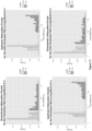
- step S3 the first and second photodetectors 70 monitor the probe signals passing along the first and second optical fibres 10, 20 respectively. Examples of the monitored probe signals in the first and second optical fibres are shown in Figure 8a and Figure 8b respectively, which illustrates the attenuations on all 64 HCF segments caused by the RF pulse.
- step S5 the greatest attenuation event in each monitored probe signal is identified (the greatest attenuation event is marked as "MAX" in Figures 8a and 8b for both the first and second optical fibres 10, 20). As discussed above, this greatest attenuation event corresponds to the attenuation caused on the probe signal passing through the HCF segment that is closest to the UE 7. The following is noted regarding terminology.
- the first optical fibre 10 has a clockwise probe signal, so that the attenuation events that are received at the first photodetector 70 in advance of the greatest attenuation event are associated with HCF segments that are in a "downstream" direction of the HCF segment associated with the greatest attenuation event, and the attenuation events that are received at the first photodetector 70 after the greatest attenuation event are associated with HCF segments that are in an "upstream" direction of the HCF segment associated with the greatest attenuation event.
- HCF segment C is downstream of HCF segment B
- HCF segment A is upstream of HCF segment B.
- the second optical fibre 20 has an counter-clockwise probe signal, so that the attenuation events that are received at the second photodetector 90 in advance of the greatest attenuation event are associated with HCF segments that are in a "downstream" direction of the HCF segment associated with the greatest attenuation event, and the attenuation events that are received at the second photodetector 90 after the greatest attenuation event are associated with HCF segments that are "upstream" of the HCF segment associated with the greatest attenuation event.
- the terms clockwise and counter-clockwise are used to describe the direction of the probe signals in the optical fibres
- the term “upstream” is used to describe points along the optical fibre that are in an opposing direction to the probe signal's direction of travel along the optical fibre
- the term “downstream” is used to describe points along the optical fibre that are in the same direction of the probe signal's direction of travel along the optical fibre.
- step S7 the base station 5 determines the reception time of the greatest attenuation event and the reception time of each of the three attenuation events immediately downstream of the greatest attenuation event and each of the three attenuation events immediately upstream of the greatest attenuation event.
- the base station 5 also records these time differences for the second optical fibre 20.
- the base station 5 then calculates the time difference between each attenuation event and its adjacent attenuation event.
- Table 1 Table illustrating the received time of attenuation events either side of the greatest attenuation event in the first and second optical fibres 10, 20 First Optical Fibre 10 Second Optical Fibre 20 Attenuation Event Attenuation Event Time Difference, ns Attenuation Event Attenuation Event Time Difference, ns N-3 N-2 109.4 N-3 N-2 130.4 N-2 N-1 38.3 N-2 N-1 42.0 N-1 MAX(N) 117.2 N-1 MAX(N) 120.8 MAX(N) N+1 -41.7 MAX(N) N+1 -41.1 N+1 N+2 -41.2 N+1 N+2 -38.1 N+2 N+3 -40.9 N+2 N+3 -37.7
- step S9 the base station 5 identifies the HCF segment associated with the greatest attenuation event (in other words, the HCF segment that is closest to the UE 7). This is achieved by, firstly, determining whether the time differences of attenuation events associated upstream and/or downstream HCF segments from the greatest attenuation event are useful data for this identification.
- the time difference between each two adjacent attenuation events are associated with either a long or short separation distance (i.e. long or short SMF segments separating two adjacent HCF segments associated with the two attenuation events). This is achieved by comparing the time difference to a classification threshold, which in this example is 90ns.
- the classification threshold is determined in the calibration phase, discussed below.
- Table 2 Table illustrating the classifications of each attenuation event based on its time difference First Optical Fibre 10 Second Optical Fibre 20 Attenuation Event Attenuation Event Class Attenuation Event Attenuation Event Class N-3 N-2 N/A N-3 N-2 Long N-2 N-1 N/A N-2 N-1 Short N-1 MAX(N) N/A N-1 MAX(N) Long MAX(N) N+1 Short MAX(N) N+1 N/A N+1 N+2 Short N+1 N+2 N/A N+2 N+3 Short N+2 N+3 N/A
- the time differences between each two adjacent attenuation events are based, in part, on the time it takes for the probe signal to travel between the HCF segments associated with each attenuation event (and thus the separation distance between these HCF segments).
- these classifications can be used as a signature to identify the HCF segment associated with the greatest attenuation event.
- the spacing classifications are long-short-long-short-short-short, or 101000 in binary.
- HCF segment 57 is identified as the HCF segment being associated with the greatest attenuation event and is therefore the closest HCF segment to the UE 7.
- RFT N is the arrival time of the RF pulse at the first HCF segment, N .
- step S13 the location of the UE 7 is determined based on the distances between the UE 7 and several HCF segments, and the locations of each of those HCF segments, using known multilateration techniques.
- the method of this first embodiment may be used to locate a UE 7 when the base station 5 is out of range of the UE.
- the base station 5 and UE 7 are out of range as wireless transmissions from the UE 7 cannot be detected by the base station's antenna above the background noise.
- base stations traditionally use dipole antennas for receiving signals from UEs.
- Rydberg atom based RF detectors may be several orders of magnitude more sensitive than traditional antennae, then the Rydberg atom based RF detector may react to a low strength transmission from the UE 7 and be processed to locate the UE 7. Once the base station 5 has determined the location of the UE 7, this information may be used to improve connectivity between the base station 5 and UE 7.
- the base station 5 may use this position information to transmit (or refine) a beam in the direction of the UE 7.
- the position may be determined at multiple time instances (by repeating the above method) in order to determine a direction of travel of the UE. This may be used to identify a base station whose coverage area will soon cover the UE, so as to enable a proactive transition mechanism or so that the base station and/or UE may configure in advance of the UE's arrival. The base station may therefore establish communications with the UE sooner than would otherwise be possible.
- the first and second optical fibres 10, 20 include 64 HCF segments separated by sections of SMF segments.
- the SMF segments may be classified as either 'long' or 'short' in length.
- the first and second optical fibres 10, 20 are manufactured to have a ratio of three long separations for every one short separation.
- the optical fibres 10, 20 are manufactured so that the combination of lengths of three SMF segments to one side of a particular HCF segment and lengths of three SMF segments to the other side of that HCF segment is unique to that HCF segment.
- step S101 of this calibration a lookup table is defined during the optical fibre manufacture which defines a signature for each HCF segment of the optical fibres 10, 20.
- step S103 the position of each HCF segment of the optical fibres 10, 20 is determined.
- the position is determined using a GNSS receiver (e.g. during a drive test).
- the lookup table from step S101 and HCF segment locations from step S103 are stored in memory on the base station 5.
- the base station 5 determines whether the upstream and downstream data for the first and second optical fibres is useful or not.
- step S105 of this calibration technique this is determined in the following manner. First, a plurality of test RF pulses are transmitted, each from a unique test location and at a unique time (both location and time data are recorded for each test RF pulse). Second, the received probe signal is detected at the first and second photodetector for each test RF pulse. Similar to the first embodiment above, the greatest attenuation event is identified in each received probe signal and the time differences between adjacent attenuation events for three upstream adjacent attenuation event pairs and three downstream adjacent attenuation event pairs are calculated.
- the separation distances between HCF segments associated with these time differences can be identified. This step is performed for each test RF pulse, resulting in a dataset correlating (for both the clockwise and counter-clockwise probe signals and for both upstream and downstream HCF segments) short separation distances with a set of time differences and long separation distances with another set of time differences.
- Figure 11 includes four histograms illustrating the density of time differences for long and short separation distances in alternative optical fibres for both clockwise and counter-clockwise probe signals. These alternative optical fibres use a ratio of four long separation distances to every one short separation distance (in contrast to the three to one ratio used in the first embodiment). It can be seen that there are gaps between the short and long classifications for each histogram, illustrating that upstream and downstream data for both optical fibres may be used. Furthermore, the skilled person will also realise that the invention may be practiced using a single optical fibre, as the upstream data and downstream data for that single optical fibre are both useful (the second optical fibre may then optionally be deployed for consistency checks or for improved accuracy).
- the time differences between three attenuation event pairs either side of the greatest attenuation event were correlated with the lookup table of separation distances between HCF segments in order to determine the identity of the HCF segment associated with the greatest attenuation event.
- This technique is preferable as these attenuation events have a greater signal to noise ratio over the background noise, reducing the error in the subsequent calculations.
- this is non-essential.
- the optical fibre is manufactured so that the combination of separation distances for each HCF segment and the (say) 5 th HCF segment on one side of that HCF segment and the (say) 4 th HCF segment on the opposing side of that HCF segment is unique to that HCF segment, and the lookup table is defined to indicate the unique combination of separation distances between each HCF segment (N) and these other HCF segments (N-5, N+4).
- the probe signal may then be analysed to identify the time difference between the greatest attenuation event and the 5 th attenuation event on one side of the greatest attenuation event, and the time difference between the greatest attenuation event and the 4 th attenuation event on the other side of the greatest attenuation event, and match these time differences to the lookup table to identify the HCF segment associated with the greatest attenuation event.
- the optical fibre should therefore be manufactured so that each HCF segment has a unique combination of separation distances with several other HCF segments, these other HCF segments having a particular sequence relationship to that HCF segment. It is also non-essential that the sequence relationship to other HCF segments is to HCF segments either side of a particular HCF segment.
- the optical fibre may be manufactured so that the combination of separation distances for each HCF segment and the (say) 5 th HCF segment on one side of that HCF segment and the (say) 4 th HCF segment on the same side of that HCF segment is unique to that HCF segment.
- the optical fibre should therefore be manufactured so that each HCF segment within the sequence of HCF segments: has a first separation distance to a first other HCF segment being a particular number of HCF segments preceding or succeeding in the sequence, has a second separation distance to a second other HCF segment being a particular number of HCF segments preceding or succeeding in the sequence, and is uniquely identified by the first and second separation distances.
- time differences are based upon the greatest attenuation event. That is, the time differences between any attenuation event and the other attenuation events (having the particular sequence relationship) may be used in the correlation to the lookup table in order to identify the HCF segment associated with that attenuation event.
- the greatest attenuation event it is beneficial to use the greatest attenuation event as it would most likely have the greatest signal to noise ratio.
- the HCF segments contain an atomic medium based on Rubidium-85 which may experience the EIT effect and have Rydberg states having energy differences that correlate with the photonic energy of frequencies used in wireless telecommunication protocols.
- the RF detector may therefore be configured to detect RF waves of a particular frequency by setting the coupling frequency to excite electrons to a particular Rydberg state, wherein the energy difference between that Rydberg state and the next Rydberg state matches the photonic energy of the RF wave to be detected.
- the skilled person will therefore understand that the use of Rubidium-85 is non-essential, and any atomic medium that may react to an RF wave so as to vary its transparency to the probe signal may be used in the above embodiment.
- the RF detector therefore does not need to be an end-to-end optical fibre, but may be any waveguide with interleaved optical fibre sections and variable transparency sections. Furthermore, it is also non-essential that the sections of optical fibre between the variable transparency sections are made of SMF (for example, multi-mode fibre may be used instead, or indeed any other waveguide).
- the detector is configured to detect electromagnetic fields in the RF band of the electromagnetic spectrum. That is, the detector may be configured so that the variable transparency section varies it transparency in response to incident electromagnetic fields of other parts of the spectrum (e.g. by using an atomic medium with particular energy states and by selecting an appropriate coupling frequency, as described above). The method of the above embodiment may therefore be used as an electromagnetic field detector.
- the probe and coupling signals are split for transmission along the first and second optical fibre.
- several probe lasers and several coupling lasers may be used to transmit the corresponding probe and coupling signals onto the first and second optical fibres respectively.
- it is non-essential for the probe and coupling signals to be counterpropagating. However, this is preferable as the Doppler shift effect may be ignored.
- the method is performed by the base station. The method may be performed by one or more suitable computing devices.
- a software-controlled programmable processing device such as a microprocessor, digital signal processor or other processing device, data processing apparatus or system
- a computer program for configuring a programmable device, apparatus or system to implement the foregoing described methods is envisaged as an aspect of the present invention.
- the computer program may be embodied as source code or undergo compilation for implementation on a processing device, apparatus or system or may be embodied as object code, for example.
- the computer program is stored on a carrier medium in machine or device readable form, for example in solid-state memory, magnetic memory such as disk or tape, optically or magneto-optically readable memory such as compact disk or digital versatile disk etc., and the processing device utilises the program or a part thereof to configure it for operation.
- the computer program may be supplied from a remote source embodied in a communications medium such as an electronic signal, radio frequency carrier wave or optical carrier wave.
- a communications medium such as an electronic signal, radio frequency carrier wave or optical carrier wave.
- carrier media are also envisaged as aspects of the present invention.
Landscapes
- Physics & Mathematics (AREA)
- General Physics & Mathematics (AREA)
- Electromagnetism (AREA)
- Engineering & Computer Science (AREA)
- Computer Networks & Wireless Communication (AREA)
- Signal Processing (AREA)
- Optics & Photonics (AREA)
- Nonlinear Science (AREA)
- Optical Communication System (AREA)
- Investigating Or Analysing Materials By Optical Means (AREA)
- Photometry And Measurement Of Optical Pulse Characteristics (AREA)
Claims (22)
- Wellenleiter (10), umfassend:eine Folge von Segmenten (13) mit variabler Transparenz, wobei jedes Segment (13) mit variabler Transparenz der Folge von Segmenten (13) mit variabler Transparenz so ausgelegt ist, dass es seine Transparenz durch den Effekt der elektromagnetisch induzierten Transparenz, EIT, ändert und seine Transparenz ferner in Reaktion auf ein auftreffendes elektromagnetisches Feld weiter ändert; undeine Mehrzahl von Trennsegmenten (11), die in die Folge von Segmenten (13) mit variabler Transparenz eingestreut ist, sodass jedes Segment (13) mit variabler Transparenz:
einen ersten Trennabstand von einem ersten anderen Segment (13) mit variabler Transparenz aufweist,der Wellenleiter dadurch gekennzeichnet ist, dass es sich bei dem ersten Trennabstand um eine erste vorbestimmte Anzahl von Segmenten mit variabler Transparenz handelt, die in der Folge von Segmenten (13) mit variabler Transparenz vorangeht oder nachfolgt,der Wellenleiter ferner dadurch gekennzeichnet ist, dass jedes Segment (13) mit variabler Transparenz:einen zweiten Trennabstand von einem zweiten anderen Segment (13) mit variabler Transparenz aufweist, wobei es sich um eine zweite vorbestimmte Anzahl von Segmenten (13) mit variabler Transparenz handelt, die in der Folge von Segmenten (13) mit variabler Transparenz vorangeht oder nachfolgt, unddurch eine Kombination von Trennabständen, die seinen ersten und seinen zweiten Trennabstand umfasst, eindeutig identifiziert wird. - Wellenleiter (10) nach Anspruch 1, wobei das erste andere Segment (13) mit variabler Transparenz in der Folge von Segmenten mit variabler Transparenz vorangeht und das zweite andere Segment (13) mit variabler Transparenz in der Folge von Segmenten (13) mit variabler Transparenz nachfolgt.
- Wellenleiter (10) nach Anspruch 2, wobei das erste andere Segment (13) mit variabler Transparenz in der Folge von Segmenten (13) mit variabler Transparenz unmittelbar vorangeht und das zweite andere Segment (13) mit variabler Transparenz in der Folge von Segmenten (13) mit variabler Transparenz unmittelbar nachfolgt.
- Wellenleiter (10) nach einem der vorhergehenden Ansprüche, wobei es sich bei dem ersten und/oder dem zweiten Trennabstand um eine Einstufung in entweder eine erste oder eine zweite Abstandskategorie handelt.
- Wellenleiter (10) nach einem der vorhergehenden Ansprüche, wobei jedes Segment (13) mit variabler Transparenz einen Metalldampf umfasst.
- Wellenleiter (10) nach Anspruch 5, wobei der Metalldampf ein Alkalimetall ist.
- Wellenleiter (10) nach Anspruch 6, wobei der Alkalimetalldampf eines ist von: Rubidium, Cäsium oder Strontium.
- Wellenleiter (10) nach einem der vorhergehenden Ansprüche, wobei jedes Segment mit variabler Transparenz ein Hohlkernfasersegment, HCF-Segment, ist.
- Wellenleiter (10) nach einem der vorhergehenden Ansprüche, wobei das elektromagnetische Feld ein Hochfrequenzfeld, HF-Feld, ist.
- System (1) mit einem ersten Wellenleiter (10) nach einem der vorhergehenden Ansprüche und einem zweiten Wellenleiter (20) nach einem der vorhergehenden Ansprüche, wobei entsprechende Segmente mit variabler Transparenz der Folge von Segmenten mit variabler Transparenz des ersten und des zweiten Wellenleiters (10, 20) ortsgleich so angeordnet sind, dass der Trennabstand zwischen jedem Paar von Segmenten mit variabler Transparenz im ersten Wellenleiter (10) gleich wie der Trennabstand zwischen jedem entsprechenden Paar von Segmenten mit variabler Transparenz im zweiten Wellenleiter (20) ist.
- Detektor für elektromagnetische Felder (1), umfassend:einen ersten optischen Sender (30),einen ersten optischen Empfänger (70), undeinen ersten Wellenleiter (10) nach einem der Ansprüche 1 bis 9, wobei:der erste optische Sender (30) und der erste optische Empfänger (70) gegenüberliegende Enden des ersten Wellenleiters (10) abschließen, undder erste optische Sender (30) ausgelegt ist zum:Senden eines Prüfsignals mit einer Prüffrequenz über den ersten Wellenleiter (10) an den ersten optischen Empfänger (70), wobei die Prüffrequenz so eingestellt ist, dass Elektronen jedes Segments (13) mit variabler Transparenz des ersten Wellenleiters (10) von einem ersten Zustand in einen zweiten Zustand angeregt werden, undSenden eines Kopplungssignals mit einer Kopplungsfrequenz über den ersten Wellenleiter (10), wobei die Kopplungsfrequenz so eingestellt ist, dass Elektronen jedes Segments (13) mit variabler Transparenz des ersten Wellenleiters (10) in einen vorbestimmten Zustand angeregt werden, um die Transparenz jedes Segments (13) mit variabler Transparenz für das Prüfsignal durch den Effekt der elektromagnetisch induzierten Transparenz, EIT, zu ändern und sodass ein elektromagnetisches Feld, das auf jedes Segment (13) mit variabler Transparenz des ersten Wellenleiters (10) auftrifft, die Transparenz des Prüfsignals an diesem Segment (13) mit variabler Transparenz weiter ändert, um eine detektierbare Änderung der Leistung des Prüfsignals am ersten optischen Empfänger (70) zu bewirken.
- Detektor für elektromagnetische Felder (1) nach Anspruch 11, ferner umfassend:einen zweiten optischen Sender;einen zweiten optischen Empfänger (90); undeinen zweiten Wellenleiter (20) nach einem der Ansprüche 1 bis 9, wobei:
entsprechende Segmente mit variabler Transparenz der Folge von Segmenten mit variabler Transparenz des ersten und des zweiten Wellenleiters (10, 20) ortsgleich so angeordnet sind, dass der Trennabstand zwischen jedem Paar von Segmenten mit variabler Transparenz im ersten Wellenleiter (10) gleich wie der Trennabstand zwischen jedem entsprechenden Paar von Segmenten mit variabler Transparenz im zweiten Wellenleiter (20) ist,der zweite optische Sender (30) und der zweite optische Empfänger (90) gegenüberliegende Enden des zweiten Wellenleiters (20) abschließen, undder zweite optische Sender ausgelegt ist zum:Senden eines zweiten Prüfsignals mit der Prüffrequenz über den zweiten Wellenleiter (20), undSenden eines zweiten Kopplungssignals mit der Kopplungsfrequenz über den zweiten Wellenleiter (20), um die Transparenz jedes Segments mit variabler Transparenz des zweiten Wellenleiters (20) für das Prüfsignal durch den EIT-Effekt zu ändern, und sodass ein elektromagnetisches Feld, das auf jedes Segment (13) mit variabler Transparenz des zweiten Wellenleiters (20) auftrifft, die Transparenz des Prüfsignals an diesem Segment (13) mit variabler Transparenz weiter ändert, um eine detektierbare Änderung der Leistung des Prüfsignals am zweiten optischen Empfänger (90) zu bewirken. - Detektor für elektromagnetische Felder (1) nach einem der Ansprüche 11 oder 12, wobei das elektromagnetische Feld ein Hochfrequenzfeld, HF-Feld, ist.
- Detektor für elektromagnetische Felder (1) nach einem der Ansprüche 12 bis 13, wobei der erste optische Sender (30) auch der zweite optische Sender ist.
- Detektor für elektromagnetische Felder (1) nach einem der Ansprüche 12 bis 14, wobei der erste optische Empfänger (70) auch der zweite optische Empfänger (90) ist.
- Verfahren zum Betreiben eines Detektors für elektromagnetische Felder, wobei der Detektor einen ersten Wellenleiter (10) nach einem der Ansprüche 1 bis 9 umfasst und das Verfahren die folgenden Schritte umfasst:Senden eines ersten Prüfsignals mit einer Prüffrequenz und einem ersten Sendeleistungswert entlang des ersten Wellenleiters (10), wobei die Prüffrequenz so eingestellt ist, dass Elektronen jedes Segments (13) mit variabler Transparenz des ersten Wellenleiters (10) von einem ersten Zustand in einen zweiten Zustand angeregt werden;Senden eines Kopplungssignals mit einer Kopplungsfrequenz entlang des ersten Wellenleiters (10), wobei die Kopplungsfrequenz so eingestellt ist, dass Elektronen jedes Segments (13) mit variabler Transparenz des ersten Wellenleiters (10) in einen vorbestimmten Zustand angeregt werden, um die Transparenz jedes Segments (13) mit variabler Transparenz des ersten Wellenleiters (10) für das erste Prüfsignal durch den Effekt der elektromagnetisch induzierten Transparenz, EIT, zu ändern und sodass ein elektromagnetisches Feld, das auf jedes Segment (13) mit variabler Transparenz des ersten Wellenleiters (10) auftrifft, die Transparenz des ersten Prüfsignals an diesem Segment (13) mit variabler Transparenz weiter ändert, um eine detektierbare Änderung der Leistung des ersten Prüfsignals zu bewirken;Überwachen des ersten Prüfsignals;Detektieren innerhalb des überwachten ersten Prüfsignals einer ersten Mehrzahl von Dämpfungsereignissen, wobei jedes Dämpfungsereignis der ersten Mehrzahl von Dämpfungsereignissen als eine Verringerung der Leistung des überwachten ersten Prüfsignals relativ zum ersten Sendeleistungswert identifizierbar ist und jedes Dämpfungsereignis der ersten Mehrzahl von Dämpfungsereignissen mit einer Empfangszeit assoziiert ist;Korrelieren der Empfangszeiten jedes Dämpfungsereignisses der ersten Mehrzahl von Dämpfungsereignissen mit der eindeutigen Kombination von Trennabständen, um jedes der ersten Mehrzahl von Dämpfungsereignissen mit einem Segment (13) mit variabler Transparenz des ersten Wellenleiters (10) zu assoziieren;Bestimmen eines Abstands zwischen jedem assoziierten Segment (13) mit variabler Transparenz und einem Sender des elektromagnetischen Feldes für eine Teilmenge der assoziierten Segmente (13) mit variabler Transparenz; undBestimmen einer Position des Senders basierend auf den bestimmten Abständen zwischen jedem assoziierten Segment mit variabler Transparenz und dem Sender.
- Verfahren nach Anspruch 16, wobei der Detektor (1) für elektromagnetische Felder ferner einen zweiten Wellenleiter (20) nach einem der Ansprüche 1 bis 9 umfasst, wobei entsprechende Segmente mit variabler Transparenz der Folge von Segmenten mit variabler Transparenz des ersten und des zweiten Wellenleiters (10, 20) ortsgleich so angeordnet sind, dass der Trennabstand zwischen jedem Paar von Segmenten mit variabler Transparenz im ersten Wellenleiter (10) gleich wie der Trennabstand zwischen jedem entsprechenden Paar von Segmenten mit variabler Transparenz im zweiten Wellenleiter (20) ist, ferner umfassend die folgenden Schritte:Senden eines zweiten Prüfsignals mit der Prüffrequenz und mit einem zweiten Sendeleistungswert entlang des zweiten Wellenleiters (20);Senden eines zweiten Kopplungssignals mit der Kopplungsfrequenz entlang des zweiten Wellenleiters (20),Überwachen des zweiten Prüfsignals; undDetektieren innerhalb des überwachten zweiten Prüfsignals einer zweiten Mehrzahl von Dämpfungsereignissen, wobei jedes Dämpfungsereignis der zweiten Mehrzahl von Dämpfungsereignissen als eine Verringerung der Leistung des überwachten zweiten Prüfsignals relativ zum zweiten Sendeleistungswert identifizierbar ist und jedes Dämpfungsereignis der zweiten Mehrzahl von Dämpfungsereignissen mit einer Empfangszeit assoziiert ist,wobei der Korrelationsschritt ein Korrelieren der Empfangszeiten von Dämpfungsereignissen entweder der ersten oder der zweiten Mehrzahl von Dämpfungsereignissen mit der eindeutigen Kombination von Trennabständen umfasst, um jedes der ersten und der zweiten Mehrzahl von Dämpfungsereignissen mit einem Segment mit variabler Transparenz des ersten oder des zweiten Wellenleiters zu assoziieren.
- Verfahren nach Anspruch 17, wobei das erste und das zweite Prüfsignal in entgegengesetzten Richtungen gesendet werden.
- Verfahren nach Anspruch 17 oder 18, ferner umfassend die folgenden Schritte:Senden eines ersten Kalibrierungsprüfsignals mit der Prüffrequenz und mit einem ersten Kalibrierungssendeleistungswert entlang des ersten Wellenleiters (10);Senden eines zweiten Kalibrierungsprüfsignals mit der Prüffrequenz und mit einem zweiten Kalibrierungssendeleistungswert entlang des zweiten Wellenleiters (20);Senden eines ersten Kalibrierungskopplungssignals mit der Kopplungsfrequenz entlang des ersten Wellenleiters (10),Senden eines zweiten Kalibrierungskopplungssignals mit der Kopplungsfrequenz entlang des zweiten Wellenleiters (20),Senden einer Mehrzahl von elektromagnetischen Kalibrierungswellen, jede von einer bekannten Position, wobei jede elektromagnetische Kalibrierungswelle der Mehrzahl von elektromagnetischen Kalibrierungswellen, die auf jedes Segment mit variabler Transparenz des ersten Wellenleiters (10) und des zweiten Wellenleiters (20) auftrifft, die Transparenz des Kalibrierungsprüfsignals an diesem Segment mit variabler Transparenz ändert, um eine detektierbare Änderung der Leistung des Kalibrierungsprüfsignals zu bewirken;Überwachen des ersten und des zweiten Kalibrierungsprüfsignals;Detektieren innerhalb des ersten und des zweiten überwachten Kalibrierungsprüfsignals einer ersten Mehrzahl von Kalibrierungsdämpfungsereignissen bzw. einer zweiten Mehrzahl von Kalibrierungsdämpfungsereignissen, wobei jedes Kalibrierungsdämpfungsereignis der ersten Mehrzahl von Kalibrierungsdämpfungsereignissen als eine Verringerung der Leistung des überwachten ersten Kalibrierungsprüfsignals relativ zum ersten Kalibrierungssendeleistungswert identifizierbar ist und jedes Kalibrierungsdämpfungsereignis der ersten Mehrzahl von Kalibrierungsdämpfungsereignissen mit einer Empfangszeit assoziiert ist, und jedes Kalibrierungsdämpfungsereignis der zweiten Mehrzahl von Kalibrierungsdämpfungsereignisse als eine Verringerung der Leistung des überwachten zweiten Kalibrierungsprüfsignals relativ zum zweiten Kalibrierungssendeleistungswert identifizierbar ist und jedes Kalibrierungsdämpfungsereignis der zweiten Mehrzahl von Kalibrierungsdämpfungsereignissen mit einer Empfangszeit assoziiert ist; undBestimmen, ob ein Dämpfungsereignis der ersten Mehrzahl von Dämpfungsereignissen des ersten überwachten Prüfsignals oder der zweiten Mehrzahl von Dämpfungsereignissen des zweiten überwachten Prüfsignals im Korrelationsschritt verwendet werden sollte, basierend auf den Empfangszeiten der ersten Mehrzahl von Kalibrierungsdämpfungsereignissen des überwachten ersten Kalibrierungsprüfsignals und den Empfangszeiten der zweiten Mehrzahl von Kalibrierungsdämpfungsereignissen des überwachten zweiten Kalibrierungsprüfsignals.
- Verfahren nach einem der Ansprüche 16 bis 19, wobei das elektromagnetische Feld ein Hochfrequenzfeld, HF-Feld, ist.
- Computerprogrammprodukt, umfassend Anweisungen, um die Vorrichtung nach Anspruch 11 zum Ausführen der Schritte des Verfahrens nach Anspruch 16 zu veranlassen.
- Computerlesbarer Datenträger, der das Computerprogramm nach Anspruch 21 darauf gespeichert aufweist.
Applications Claiming Priority (3)
| Application Number | Priority Date | Filing Date | Title |
|---|---|---|---|
| GB1915420.2A GB2588754B (en) | 2019-10-24 | 2019-10-24 | Wireless telecommunications network |
| EP19205106 | 2019-10-24 | ||
| PCT/EP2020/075070 WO2021078438A1 (en) | 2019-10-24 | 2020-09-08 | Wireless telecommunications network |
Publications (3)
| Publication Number | Publication Date |
|---|---|
| EP4005116A1 EP4005116A1 (de) | 2022-06-01 |
| EP4005116B1 true EP4005116B1 (de) | 2024-08-21 |
| EP4005116B8 EP4005116B8 (de) | 2024-10-02 |
Family
ID=72322476
Family Applications (1)
| Application Number | Title | Priority Date | Filing Date |
|---|---|---|---|
| EP20765052.4A Active EP4005116B8 (de) | 2019-10-24 | 2020-09-08 | Drahtloses telekommunikationsnetzwerk |
Country Status (4)
| Country | Link |
|---|---|
| US (1) | US11835564B2 (de) |
| EP (1) | EP4005116B8 (de) |
| CN (1) | CN114424111B (de) |
| WO (1) | WO2021078438A1 (de) |
Families Citing this family (12)
| Publication number | Priority date | Publication date | Assignee | Title |
|---|---|---|---|---|
| EP4005116B8 (de) | 2019-10-24 | 2024-10-02 | British Telecommunications public limited company | Drahtloses telekommunikationsnetzwerk |
| GB2597260B (en) | 2020-07-16 | 2022-12-07 | British Telecomm | Electromagnetic field receiver |
| GB2605123B (en) | 2021-03-01 | 2023-04-26 | British Telecomm | Electromagnetic field detector |
| GB2605651A (en) * | 2021-04-09 | 2022-10-12 | British Telecomm | Electromagnetic field receiver |
| GB2605650B (en) | 2021-04-09 | 2023-06-07 | British Telecomm | Electromagnetic field detector |
| GB2606167B (en) | 2021-04-27 | 2023-06-21 | British Telecomm | Wireless transceiver |
| US11843420B1 (en) | 2021-09-10 | 2023-12-12 | ColdQuanta, Inc. | Radio-frequency receiver pumped to high-azimuthal rydberg states |
| US12032010B1 (en) | 2021-09-10 | 2024-07-09 | ColdQuanta, Inc. | Deployable Rydberg RF sensor |
| US12411162B2 (en) | 2022-08-10 | 2025-09-09 | British Telecommunications Public Limited Company | Electromagnetic field detector |
| EP4573682A1 (de) * | 2022-08-17 | 2025-06-25 | British Telecommunications Public Limited Company | Netzwerkknoten |
| GB2624368B (en) * | 2022-11-08 | 2024-12-18 | British Telecomm | Electromagnetic field detector |
| US20260009835A1 (en) * | 2022-11-08 | 2026-01-08 | British Telecommunications Public Limited Company | Electromagnetic field detector |
Family Cites Families (31)
| Publication number | Priority date | Publication date | Assignee | Title |
|---|---|---|---|---|
| US6826339B1 (en) * | 2003-11-14 | 2004-11-30 | Corning Incorporated | Electromagnetically induced transparent (EIT) photonic band-gap fibers |
| US8005332B2 (en) | 2007-05-09 | 2011-08-23 | The Regents Of The University Of California | Integrated optical vapor cell apparatus for precision spectroscopy |
| US8054073B2 (en) | 2008-05-21 | 2011-11-08 | Entanglement Technologies, Llc | Method and apparatus for implementing EIT magnetometry |
| JP2011089868A (ja) | 2009-10-22 | 2011-05-06 | Seiko Epson Corp | ファイバーセル、磁気センサー、及び磁界測定装置 |
| US9651504B2 (en) * | 2014-07-30 | 2017-05-16 | B.G. Negev Technologies And Applications Ltd., At Ben-Gurion University | Fano resonance microwave spectroscopy of high absorption matter |
| CN104714110B (zh) | 2015-04-02 | 2017-09-26 | 山西大学 | 基于电磁诱导透明效应测量高频微波场强的装置和方法 |
| WO2016205330A1 (en) | 2015-06-15 | 2016-12-22 | The Regents Of The University Of Michigan | Atom-based electromagnetic radiation electric-field sensor |
| CN205691490U (zh) | 2016-06-21 | 2016-11-16 | 中国计量大学 | 一种基于游标效应的级联型fpi氢气传感器 |
| CN106124856B (zh) | 2016-07-25 | 2018-10-26 | 山西大学 | 直接溯源至原子高激发态间跃迁频率的射频源校准方法 |
| JP6898448B2 (ja) | 2016-12-09 | 2021-07-07 | テレフオンアクチーボラゲット エルエム エリクソン(パブル) | 分散マッシブmimoのための改良されたアンテナ装置 |
| CN108152602B (zh) | 2016-12-15 | 2021-11-26 | 中国计量科学研究院 | 一种基于量子相干效应的天线增益测量装置 |
| CN107179450B (zh) | 2017-05-31 | 2019-10-11 | 华南师范大学 | 一种微波电场强度测量方法和测量装置 |
| CN107462849B (zh) * | 2017-07-21 | 2020-01-03 | 山西大学 | 一种基于原子能级的射频线传输因子的测量装置及方法 |
| CN112867934A (zh) | 2017-12-18 | 2021-05-28 | 里德堡技术公司 | 基于原子的电磁场感测元件与测量系统 |
| CN108809341B (zh) | 2018-05-25 | 2020-04-17 | 山西大学 | 一种基于里德堡原子的量子天线调频波接收装置和方法 |
| CN108927314B (zh) | 2018-07-25 | 2020-06-30 | 哈尔滨工业大学(深圳) | 一种基于无芯光纤的分布式光纤激光超声换能装置 |
| CN109142891A (zh) | 2018-09-25 | 2019-01-04 | 北京理工大学 | 基于里德堡原子量子相干效应的天线近场测试探头及方法 |
| CN109342830B (zh) | 2018-10-23 | 2021-07-02 | 山西大学 | 全光纤马赫曾德尔干涉仪的微波场强原子测量装置 |
| US10979147B2 (en) * | 2019-03-11 | 2021-04-13 | Government Of The United States Of America, As Represented By The Secretary Of Commerce | Rydberg atom mixer and determining phase of modulated carrier radiation |
| CN109905177A (zh) | 2019-03-13 | 2019-06-18 | 华南师范大学 | 基于微波光波相干转换的无线数字通信接收天线及其方法 |
| US10763966B1 (en) | 2019-03-25 | 2020-09-01 | Otago Innovation Limited | Data communications system using an optical antenna |
| GB2588754B (en) | 2019-10-24 | 2022-05-11 | British Telecomm | Wireless telecommunications network |
| EP4005116B8 (de) | 2019-10-24 | 2024-10-02 | British Telecommunications public limited company | Drahtloses telekommunikationsnetzwerk |
| US11165505B2 (en) | 2020-02-12 | 2021-11-02 | Government Of The United States Of America, As Represented By The Secretary Of Commerce | Quantum atomic receiving antenna and quantum sensing of radiofrequency radiation |
| CA3178752A1 (en) | 2020-05-29 | 2021-12-02 | David A. Anderson | Atom-based closed-loop control for electromagnetic radiation measurement, communications, and information processing |
| GB2597260B (en) | 2020-07-16 | 2022-12-07 | British Telecomm | Electromagnetic field receiver |
| CN113514698B (zh) | 2021-03-01 | 2024-05-17 | 中国科学院大学 | 一种测量微波相位的装置和方法 |
| GB2605123B (en) | 2021-03-01 | 2023-04-26 | British Telecomm | Electromagnetic field detector |
| GB2606167B (en) | 2021-04-27 | 2023-06-21 | British Telecomm | Wireless transceiver |
| CN113504415B (zh) | 2021-06-01 | 2023-07-21 | 中国科学院大学 | 一种里德堡原子微波鉴相器系统及其相位测量方法 |
| US11402479B1 (en) | 2022-02-08 | 2022-08-02 | Quantum Valley Ideas Laboratories | Communicating information using photonic crystal transceivers |
-
2020
- 2020-09-08 EP EP20765052.4A patent/EP4005116B8/de active Active
- 2020-09-08 WO PCT/EP2020/075070 patent/WO2021078438A1/en not_active Ceased
- 2020-09-08 US US17/754,871 patent/US11835564B2/en active Active
- 2020-09-08 CN CN202080066526.3A patent/CN114424111B/zh active Active
Also Published As
| Publication number | Publication date |
|---|---|
| US11835564B2 (en) | 2023-12-05 |
| EP4005116A1 (de) | 2022-06-01 |
| US20230194590A1 (en) | 2023-06-22 |
| CN114424111A (zh) | 2022-04-29 |
| CN114424111B (zh) | 2022-12-27 |
| EP4005116B8 (de) | 2024-10-02 |
| WO2021078438A1 (en) | 2021-04-29 |
Similar Documents
| Publication | Publication Date | Title |
|---|---|---|
| EP4005116B1 (de) | Drahtloses telekommunikationsnetzwerk | |
| GB2588754A (en) | Wireless telecommunications network | |
| US10989587B2 (en) | Distributed fibre sensing system and vibration detection and positioning method therefor | |
| US9180357B2 (en) | Multiple antenna interference rejection in ultra-wideband real time locating systems | |
| EP4137825B1 (de) | Sensorempfänger mit einer rydbergzelle und beabstandeten gepulsten sondenstrahlen und zugehörige verfahren | |
| CN117157539B (zh) | 电磁场接收器 | |
| CN117256112A (zh) | 无线收发器 | |
| CN101688913A (zh) | 用于确定远程通信设备之间的视距(los)距离的方法 | |
| GB2624368A (en) | Electromagnetic field detector | |
| US20260009835A1 (en) | Electromagnetic field detector | |
| EP4320451B1 (de) | Detektor für elektromagnetisches feld | |
| CA1165908A (en) | Method and apparatus for measuring signal to noise ratio in a tdma communications system | |
| EP1756979B1 (de) | Gepulstes rückschleif-signalisierungsverfahren mit hohen verlusten | |
| US12289135B2 (en) | Electromagnetic field detector | |
| Zaisberger et al. | Random access performance evaluation and improvements of the LDACS | |
| US10389402B1 (en) | Background noise floor thresholds for frequency hopping systems | |
| JP2000111641A (ja) | 放送機能付dmeシステム | |
| Hollis | An experimental equipment to reduce teleprinter errors in the presence of multipath | |
| EP0455411B1 (de) | Korrelationsdetektor für FM-Signale | |
| RU2446588C2 (ru) | Способ радиосвязи | |
| Soghomonian et al. | Experimental studies of a new power divider for integrated optics | |
| JPS60115881A (ja) | 受信装置 |
Legal Events
| Date | Code | Title | Description |
|---|---|---|---|
| STAA | Information on the status of an ep patent application or granted ep patent |
Free format text: STATUS: UNKNOWN |
|
| STAA | Information on the status of an ep patent application or granted ep patent |
Free format text: STATUS: THE INTERNATIONAL PUBLICATION HAS BEEN MADE |
|
| PUAI | Public reference made under article 153(3) epc to a published international application that has entered the european phase |
Free format text: ORIGINAL CODE: 0009012 |
|
| STAA | Information on the status of an ep patent application or granted ep patent |
Free format text: STATUS: REQUEST FOR EXAMINATION WAS MADE |
|
| 17P | Request for examination filed |
Effective date: 20220224 |
|
| AK | Designated contracting states |
Kind code of ref document: A1 Designated state(s): AL AT BE BG CH CY CZ DE DK EE ES FI FR GB GR HR HU IE IS IT LI LT LU LV MC MK MT NL NO PL PT RO RS SE SI SK SM TR |
|
| STAA | Information on the status of an ep patent application or granted ep patent |
Free format text: STATUS: EXAMINATION IS IN PROGRESS |
|
| 17Q | First examination report despatched |
Effective date: 20220816 |
|
| DAV | Request for validation of the european patent (deleted) | ||
| DAX | Request for extension of the european patent (deleted) | ||
| P01 | Opt-out of the competence of the unified patent court (upc) registered |
Effective date: 20230623 |
|
| GRAP | Despatch of communication of intention to grant a patent |
Free format text: ORIGINAL CODE: EPIDOSNIGR1 |
|
| STAA | Information on the status of an ep patent application or granted ep patent |
Free format text: STATUS: GRANT OF PATENT IS INTENDED |
|
| RIC1 | Information provided on ipc code assigned before grant |
Ipc: G01R 29/08 20060101ALI20240220BHEP Ipc: G02B 6/02 20060101ALI20240220BHEP Ipc: H04B 17/00 20150101AFI20240220BHEP |
|
| INTG | Intention to grant announced |
Effective date: 20240327 |
|
| GRAS | Grant fee paid |
Free format text: ORIGINAL CODE: EPIDOSNIGR3 |
|
| GRAA | (expected) grant |
Free format text: ORIGINAL CODE: 0009210 |
|
| STAA | Information on the status of an ep patent application or granted ep patent |
Free format text: STATUS: THE PATENT HAS BEEN GRANTED |
|
| AK | Designated contracting states |
Kind code of ref document: B1 Designated state(s): AL AT BE BG CH CY CZ DE DK EE ES FI FR GB GR HR HU IE IS IT LI LT LU LV MC MK MT NL NO PL PT RO RS SE SI SK SM TR |
|
| REG | Reference to a national code |
Ref country code: GB Ref legal event code: FG4D |
|
| RBV | Designated contracting states (corrected) |
Designated state(s): AL AT BE BG CH CY CZ DE DK EE ES FI FR GR HR HU IE IS IT LI LT LU LV MC MK MT NL NO PL PT RO RS SE SI SK SM TR |
|
| REG | Reference to a national code |
Ref country code: CH Ref legal event code: EP |
|
| REG | Reference to a national code |
Ref country code: IE Ref legal event code: FG4D |
|
| REG | Reference to a national code |
Ref country code: DE Ref legal event code: R096 Ref document number: 602020036267 Country of ref document: DE |
|
| REG | Reference to a national code |
Ref country code: CH Ref legal event code: PK Free format text: BERICHTIGUNG B8 |
|
| REG | Reference to a national code |
Ref country code: LT Ref legal event code: MG9D |
|
| REG | Reference to a national code |
Ref country code: NL Ref legal event code: MP Effective date: 20240821 |
|
| PG25 | Lapsed in a contracting state [announced via postgrant information from national office to epo] |
Ref country code: NO Free format text: LAPSE BECAUSE OF FAILURE TO SUBMIT A TRANSLATION OF THE DESCRIPTION OR TO PAY THE FEE WITHIN THE PRESCRIBED TIME-LIMIT Effective date: 20241121 |
|
| REG | Reference to a national code |
Ref country code: AT Ref legal event code: MK05 Ref document number: 1716551 Country of ref document: AT Kind code of ref document: T Effective date: 20240821 |
|
| PG25 | Lapsed in a contracting state [announced via postgrant information from national office to epo] |
Ref country code: FI Free format text: LAPSE BECAUSE OF FAILURE TO SUBMIT A TRANSLATION OF THE DESCRIPTION OR TO PAY THE FEE WITHIN THE PRESCRIBED TIME-LIMIT Effective date: 20240821 Ref country code: NL Free format text: LAPSE BECAUSE OF FAILURE TO SUBMIT A TRANSLATION OF THE DESCRIPTION OR TO PAY THE FEE WITHIN THE PRESCRIBED TIME-LIMIT Effective date: 20240821 Ref country code: PL Free format text: LAPSE BECAUSE OF FAILURE TO SUBMIT A TRANSLATION OF THE DESCRIPTION OR TO PAY THE FEE WITHIN THE PRESCRIBED TIME-LIMIT Effective date: 20240821 Ref country code: PT Free format text: LAPSE BECAUSE OF FAILURE TO SUBMIT A TRANSLATION OF THE DESCRIPTION OR TO PAY THE FEE WITHIN THE PRESCRIBED TIME-LIMIT Effective date: 20241223 Ref country code: GR Free format text: LAPSE BECAUSE OF FAILURE TO SUBMIT A TRANSLATION OF THE DESCRIPTION OR TO PAY THE FEE WITHIN THE PRESCRIBED TIME-LIMIT Effective date: 20241122 |
|
| PG25 | Lapsed in a contracting state [announced via postgrant information from national office to epo] |
Ref country code: BG Free format text: LAPSE BECAUSE OF FAILURE TO SUBMIT A TRANSLATION OF THE DESCRIPTION OR TO PAY THE FEE WITHIN THE PRESCRIBED TIME-LIMIT Effective date: 20240821 |
|
| PG25 | Lapsed in a contracting state [announced via postgrant information from national office to epo] |
Ref country code: LV Free format text: LAPSE BECAUSE OF FAILURE TO SUBMIT A TRANSLATION OF THE DESCRIPTION OR TO PAY THE FEE WITHIN THE PRESCRIBED TIME-LIMIT Effective date: 20240821 |
|
| PG25 | Lapsed in a contracting state [announced via postgrant information from national office to epo] |
Ref country code: IS Free format text: LAPSE BECAUSE OF FAILURE TO SUBMIT A TRANSLATION OF THE DESCRIPTION OR TO PAY THE FEE WITHIN THE PRESCRIBED TIME-LIMIT Effective date: 20241221 Ref country code: AT Free format text: LAPSE BECAUSE OF FAILURE TO SUBMIT A TRANSLATION OF THE DESCRIPTION OR TO PAY THE FEE WITHIN THE PRESCRIBED TIME-LIMIT Effective date: 20240821 |
|
| PG25 | Lapsed in a contracting state [announced via postgrant information from national office to epo] |
Ref country code: HR Free format text: LAPSE BECAUSE OF FAILURE TO SUBMIT A TRANSLATION OF THE DESCRIPTION OR TO PAY THE FEE WITHIN THE PRESCRIBED TIME-LIMIT Effective date: 20240821 |
|
| PG25 | Lapsed in a contracting state [announced via postgrant information from national office to epo] |
Ref country code: ES Free format text: LAPSE BECAUSE OF FAILURE TO SUBMIT A TRANSLATION OF THE DESCRIPTION OR TO PAY THE FEE WITHIN THE PRESCRIBED TIME-LIMIT Effective date: 20240821 Ref country code: RS Free format text: LAPSE BECAUSE OF FAILURE TO SUBMIT A TRANSLATION OF THE DESCRIPTION OR TO PAY THE FEE WITHIN THE PRESCRIBED TIME-LIMIT Effective date: 20241121 |
|
| PG25 | Lapsed in a contracting state [announced via postgrant information from national office to epo] |
Ref country code: RS Free format text: LAPSE BECAUSE OF FAILURE TO SUBMIT A TRANSLATION OF THE DESCRIPTION OR TO PAY THE FEE WITHIN THE PRESCRIBED TIME-LIMIT Effective date: 20241121 Ref country code: PT Free format text: LAPSE BECAUSE OF FAILURE TO SUBMIT A TRANSLATION OF THE DESCRIPTION OR TO PAY THE FEE WITHIN THE PRESCRIBED TIME-LIMIT Effective date: 20241223 Ref country code: PL Free format text: LAPSE BECAUSE OF FAILURE TO SUBMIT A TRANSLATION OF THE DESCRIPTION OR TO PAY THE FEE WITHIN THE PRESCRIBED TIME-LIMIT Effective date: 20240821 Ref country code: NO Free format text: LAPSE BECAUSE OF FAILURE TO SUBMIT A TRANSLATION OF THE DESCRIPTION OR TO PAY THE FEE WITHIN THE PRESCRIBED TIME-LIMIT Effective date: 20241121 Ref country code: NL Free format text: LAPSE BECAUSE OF FAILURE TO SUBMIT A TRANSLATION OF THE DESCRIPTION OR TO PAY THE FEE WITHIN THE PRESCRIBED TIME-LIMIT Effective date: 20240821 Ref country code: LV Free format text: LAPSE BECAUSE OF FAILURE TO SUBMIT A TRANSLATION OF THE DESCRIPTION OR TO PAY THE FEE WITHIN THE PRESCRIBED TIME-LIMIT Effective date: 20240821 Ref country code: IS Free format text: LAPSE BECAUSE OF FAILURE TO SUBMIT A TRANSLATION OF THE DESCRIPTION OR TO PAY THE FEE WITHIN THE PRESCRIBED TIME-LIMIT Effective date: 20241221 Ref country code: HR Free format text: LAPSE BECAUSE OF FAILURE TO SUBMIT A TRANSLATION OF THE DESCRIPTION OR TO PAY THE FEE WITHIN THE PRESCRIBED TIME-LIMIT Effective date: 20240821 Ref country code: GR Free format text: LAPSE BECAUSE OF FAILURE TO SUBMIT A TRANSLATION OF THE DESCRIPTION OR TO PAY THE FEE WITHIN THE PRESCRIBED TIME-LIMIT Effective date: 20241122 Ref country code: FI Free format text: LAPSE BECAUSE OF FAILURE TO SUBMIT A TRANSLATION OF THE DESCRIPTION OR TO PAY THE FEE WITHIN THE PRESCRIBED TIME-LIMIT Effective date: 20240821 Ref country code: ES Free format text: LAPSE BECAUSE OF FAILURE TO SUBMIT A TRANSLATION OF THE DESCRIPTION OR TO PAY THE FEE WITHIN THE PRESCRIBED TIME-LIMIT Effective date: 20240821 Ref country code: BG Free format text: LAPSE BECAUSE OF FAILURE TO SUBMIT A TRANSLATION OF THE DESCRIPTION OR TO PAY THE FEE WITHIN THE PRESCRIBED TIME-LIMIT Effective date: 20240821 Ref country code: AT Free format text: LAPSE BECAUSE OF FAILURE TO SUBMIT A TRANSLATION OF THE DESCRIPTION OR TO PAY THE FEE WITHIN THE PRESCRIBED TIME-LIMIT Effective date: 20240821 |
|
| PG25 | Lapsed in a contracting state [announced via postgrant information from national office to epo] |
Ref country code: RO Free format text: LAPSE BECAUSE OF FAILURE TO SUBMIT A TRANSLATION OF THE DESCRIPTION OR TO PAY THE FEE WITHIN THE PRESCRIBED TIME-LIMIT Effective date: 20240821 Ref country code: SM Free format text: LAPSE BECAUSE OF FAILURE TO SUBMIT A TRANSLATION OF THE DESCRIPTION OR TO PAY THE FEE WITHIN THE PRESCRIBED TIME-LIMIT Effective date: 20240821 Ref country code: DK Free format text: LAPSE BECAUSE OF FAILURE TO SUBMIT A TRANSLATION OF THE DESCRIPTION OR TO PAY THE FEE WITHIN THE PRESCRIBED TIME-LIMIT Effective date: 20240821 |
|
| PG25 | Lapsed in a contracting state [announced via postgrant information from national office to epo] |
Ref country code: CZ Free format text: LAPSE BECAUSE OF FAILURE TO SUBMIT A TRANSLATION OF THE DESCRIPTION OR TO PAY THE FEE WITHIN THE PRESCRIBED TIME-LIMIT Effective date: 20240821 |
|
| PG25 | Lapsed in a contracting state [announced via postgrant information from national office to epo] |
Ref country code: SK Free format text: LAPSE BECAUSE OF FAILURE TO SUBMIT A TRANSLATION OF THE DESCRIPTION OR TO PAY THE FEE WITHIN THE PRESCRIBED TIME-LIMIT Effective date: 20240821 Ref country code: IT Free format text: LAPSE BECAUSE OF FAILURE TO SUBMIT A TRANSLATION OF THE DESCRIPTION OR TO PAY THE FEE WITHIN THE PRESCRIBED TIME-LIMIT Effective date: 20240821 |
|
| REG | Reference to a national code |
Ref country code: CH Ref legal event code: PL |
|
| PG25 | Lapsed in a contracting state [announced via postgrant information from national office to epo] |
Ref country code: LU Free format text: LAPSE BECAUSE OF NON-PAYMENT OF DUE FEES Effective date: 20240908 |
|
| REG | Reference to a national code |
Ref country code: DE Ref legal event code: R097 Ref document number: 602020036267 Country of ref document: DE |
|
| PLBE | No opposition filed within time limit |
Free format text: ORIGINAL CODE: 0009261 |
|
| STAA | Information on the status of an ep patent application or granted ep patent |
Free format text: STATUS: NO OPPOSITION FILED WITHIN TIME LIMIT |
|
| PG25 | Lapsed in a contracting state [announced via postgrant information from national office to epo] |
Ref country code: MC Free format text: LAPSE BECAUSE OF FAILURE TO SUBMIT A TRANSLATION OF THE DESCRIPTION OR TO PAY THE FEE WITHIN THE PRESCRIBED TIME-LIMIT Effective date: 20240821 |
|
| REG | Reference to a national code |
Ref country code: BE Ref legal event code: MM Effective date: 20240930 |
|
| PG25 | Lapsed in a contracting state [announced via postgrant information from national office to epo] |
Ref country code: BE Free format text: LAPSE BECAUSE OF NON-PAYMENT OF DUE FEES Effective date: 20240930 |
|
| PG25 | Lapsed in a contracting state [announced via postgrant information from national office to epo] |
Ref country code: CH Free format text: LAPSE BECAUSE OF NON-PAYMENT OF DUE FEES Effective date: 20240930 |
|
| PG25 | Lapsed in a contracting state [announced via postgrant information from national office to epo] |
Ref country code: IE Free format text: LAPSE BECAUSE OF NON-PAYMENT OF DUE FEES Effective date: 20240908 |
|
| 26N | No opposition filed |
Effective date: 20250522 |
|
| PG25 | Lapsed in a contracting state [announced via postgrant information from national office to epo] |
Ref country code: SE Free format text: LAPSE BECAUSE OF FAILURE TO SUBMIT A TRANSLATION OF THE DESCRIPTION OR TO PAY THE FEE WITHIN THE PRESCRIBED TIME-LIMIT Effective date: 20240821 |
|
| PGFP | Annual fee paid to national office [announced via postgrant information from national office to epo] |
Ref country code: DE Payment date: 20250820 Year of fee payment: 6 |
|
| PGFP | Annual fee paid to national office [announced via postgrant information from national office to epo] |
Ref country code: FR Payment date: 20250820 Year of fee payment: 6 |
|
| PG25 | Lapsed in a contracting state [announced via postgrant information from national office to epo] |
Ref country code: CY Free format text: LAPSE BECAUSE OF FAILURE TO SUBMIT A TRANSLATION OF THE DESCRIPTION OR TO PAY THE FEE WITHIN THE PRESCRIBED TIME-LIMIT; INVALID AB INITIO Effective date: 20200908 |