EP4002178B1 - Unterstützung von speicher-paging in virtualisierten systemen unter verwendung von vertrauensdomänen - Google Patents
Unterstützung von speicher-paging in virtualisierten systemen unter verwendung von vertrauensdomänen Download PDFInfo
- Publication number
- EP4002178B1 EP4002178B1 EP22151703.0A EP22151703A EP4002178B1 EP 4002178 B1 EP4002178 B1 EP 4002178B1 EP 22151703 A EP22151703 A EP 22151703A EP 4002178 B1 EP4002178 B1 EP 4002178B1
- Authority
- EP
- European Patent Office
- Prior art keywords
- memory
- page
- transportable
- contents
- processing device
- Prior art date
- Legal status (The legal status is an assumption and is not a legal conclusion. Google has not performed a legal analysis and makes no representation as to the accuracy of the status listed.)
- Active
Links
Images







Classifications
-
- G—PHYSICS
- G06—COMPUTING OR CALCULATING; COUNTING
- G06F—ELECTRIC DIGITAL DATA PROCESSING
- G06F9/00—Arrangements for program control, e.g. control units
- G06F9/06—Arrangements for program control, e.g. control units using stored programs, i.e. using an internal store of processing equipment to receive or retain programs
- G06F9/44—Arrangements for executing specific programs
- G06F9/455—Emulation; Interpretation; Software simulation, e.g. virtualisation or emulation of application or operating system execution engines
- G06F9/45533—Hypervisors; Virtual machine monitors
- G06F9/45558—Hypervisor-specific management and integration aspects
-
- G—PHYSICS
- G06—COMPUTING OR CALCULATING; COUNTING
- G06F—ELECTRIC DIGITAL DATA PROCESSING
- G06F12/00—Accessing, addressing or allocating within memory systems or architectures
- G06F12/02—Addressing or allocation; Relocation
- G06F12/08—Addressing or allocation; Relocation in hierarchically structured memory systems, e.g. virtual memory systems
-
- G—PHYSICS
- G06—COMPUTING OR CALCULATING; COUNTING
- G06F—ELECTRIC DIGITAL DATA PROCESSING
- G06F12/00—Accessing, addressing or allocating within memory systems or architectures
- G06F12/02—Addressing or allocation; Relocation
- G06F12/08—Addressing or allocation; Relocation in hierarchically structured memory systems, e.g. virtual memory systems
- G06F12/0802—Addressing of a memory level in which the access to the desired data or data block requires associative addressing means, e.g. caches
- G06F12/0891—Addressing of a memory level in which the access to the desired data or data block requires associative addressing means, e.g. caches using clearing, invalidating or resetting means
-
- G—PHYSICS
- G06—COMPUTING OR CALCULATING; COUNTING
- G06F—ELECTRIC DIGITAL DATA PROCESSING
- G06F12/00—Accessing, addressing or allocating within memory systems or architectures
- G06F12/02—Addressing or allocation; Relocation
- G06F12/08—Addressing or allocation; Relocation in hierarchically structured memory systems, e.g. virtual memory systems
- G06F12/10—Address translation
- G06F12/1009—Address translation using page tables, e.g. page table structures
-
- G—PHYSICS
- G06—COMPUTING OR CALCULATING; COUNTING
- G06F—ELECTRIC DIGITAL DATA PROCESSING
- G06F12/00—Accessing, addressing or allocating within memory systems or architectures
- G06F12/02—Addressing or allocation; Relocation
- G06F12/08—Addressing or allocation; Relocation in hierarchically structured memory systems, e.g. virtual memory systems
- G06F12/10—Address translation
- G06F12/109—Address translation for multiple virtual address spaces, e.g. segmentation
-
- G—PHYSICS
- G06—COMPUTING OR CALCULATING; COUNTING
- G06F—ELECTRIC DIGITAL DATA PROCESSING
- G06F12/00—Accessing, addressing or allocating within memory systems or architectures
- G06F12/02—Addressing or allocation; Relocation
- G06F12/08—Addressing or allocation; Relocation in hierarchically structured memory systems, e.g. virtual memory systems
- G06F12/12—Replacement control
- G06F12/121—Replacement control using replacement algorithms
-
- G—PHYSICS
- G06—COMPUTING OR CALCULATING; COUNTING
- G06F—ELECTRIC DIGITAL DATA PROCESSING
- G06F12/00—Accessing, addressing or allocating within memory systems or architectures
- G06F12/14—Protection against unauthorised use of memory or access to memory
- G06F12/1408—Protection against unauthorised use of memory or access to memory by using cryptography
-
- G—PHYSICS
- G06—COMPUTING OR CALCULATING; COUNTING
- G06F—ELECTRIC DIGITAL DATA PROCESSING
- G06F12/00—Accessing, addressing or allocating within memory systems or architectures
- G06F12/14—Protection against unauthorised use of memory or access to memory
- G06F12/1416—Protection against unauthorised use of memory or access to memory by checking the object accessibility, e.g. type of access defined by the memory independently of subject rights
- G06F12/1425—Protection against unauthorised use of memory or access to memory by checking the object accessibility, e.g. type of access defined by the memory independently of subject rights the protection being physical, e.g. cell, word, block
- G06F12/1441—Protection against unauthorised use of memory or access to memory by checking the object accessibility, e.g. type of access defined by the memory independently of subject rights the protection being physical, e.g. cell, word, block for a range
-
- G—PHYSICS
- G06—COMPUTING OR CALCULATING; COUNTING
- G06F—ELECTRIC DIGITAL DATA PROCESSING
- G06F12/00—Accessing, addressing or allocating within memory systems or architectures
- G06F12/14—Protection against unauthorised use of memory or access to memory
- G06F12/1458—Protection against unauthorised use of memory or access to memory by checking the subject access rights
- G06F12/1466—Key-lock mechanism
-
- G—PHYSICS
- G06—COMPUTING OR CALCULATING; COUNTING
- G06F—ELECTRIC DIGITAL DATA PROCESSING
- G06F21/00—Security arrangements for protecting computers, components thereof, programs or data against unauthorised activity
- G06F21/60—Protecting data
- G06F21/62—Protecting access to data via a platform, e.g. using keys or access control rules
- G06F21/6218—Protecting access to data via a platform, e.g. using keys or access control rules to a system of files or objects, e.g. local or distributed file system or database
- G06F21/6281—Protecting access to data via a platform, e.g. using keys or access control rules to a system of files or objects, e.g. local or distributed file system or database at program execution time, where the protection is within the operating system
-
- G—PHYSICS
- G06—COMPUTING OR CALCULATING; COUNTING
- G06F—ELECTRIC DIGITAL DATA PROCESSING
- G06F21/00—Security arrangements for protecting computers, components thereof, programs or data against unauthorised activity
- G06F21/70—Protecting specific internal or peripheral components, in which the protection of a component leads to protection of the entire computer
- G06F21/78—Protecting specific internal or peripheral components, in which the protection of a component leads to protection of the entire computer to assure secure storage of data
- G06F21/79—Protecting specific internal or peripheral components, in which the protection of a component leads to protection of the entire computer to assure secure storage of data in semiconductor storage media, e.g. directly-addressable memories
-
- G—PHYSICS
- G06—COMPUTING OR CALCULATING; COUNTING
- G06F—ELECTRIC DIGITAL DATA PROCESSING
- G06F12/00—Accessing, addressing or allocating within memory systems or architectures
- G06F12/02—Addressing or allocation; Relocation
- G06F12/08—Addressing or allocation; Relocation in hierarchically structured memory systems, e.g. virtual memory systems
- G06F12/10—Address translation
- G06F12/1027—Address translation using associative or pseudo-associative address translation means, e.g. translation look-aside buffer [TLB]
- G06F12/1036—Address translation using associative or pseudo-associative address translation means, e.g. translation look-aside buffer [TLB] for multiple virtual address spaces, e.g. segmentation
-
- G—PHYSICS
- G06—COMPUTING OR CALCULATING; COUNTING
- G06F—ELECTRIC DIGITAL DATA PROCESSING
- G06F9/00—Arrangements for program control, e.g. control units
- G06F9/06—Arrangements for program control, e.g. control units using stored programs, i.e. using an internal store of processing equipment to receive or retain programs
- G06F9/44—Arrangements for executing specific programs
- G06F9/455—Emulation; Interpretation; Software simulation, e.g. virtualisation or emulation of application or operating system execution engines
- G06F9/45533—Hypervisors; Virtual machine monitors
- G06F9/45558—Hypervisor-specific management and integration aspects
- G06F2009/45583—Memory management, e.g. access or allocation
-
- G—PHYSICS
- G06—COMPUTING OR CALCULATING; COUNTING
- G06F—ELECTRIC DIGITAL DATA PROCESSING
- G06F2212/00—Indexing scheme relating to accessing, addressing or allocation within memory systems or architectures
- G06F2212/10—Providing a specific technical effect
- G06F2212/1052—Security improvement
-
- G—PHYSICS
- G06—COMPUTING OR CALCULATING; COUNTING
- G06F—ELECTRIC DIGITAL DATA PROCESSING
- G06F2212/00—Indexing scheme relating to accessing, addressing or allocation within memory systems or architectures
- G06F2212/15—Use in a specific computing environment
- G06F2212/152—Virtualized environment, e.g. logically partitioned system
-
- G—PHYSICS
- G06—COMPUTING OR CALCULATING; COUNTING
- G06F—ELECTRIC DIGITAL DATA PROCESSING
- G06F2212/00—Indexing scheme relating to accessing, addressing or allocation within memory systems or architectures
- G06F2212/65—Details of virtual memory and virtual address translation
- G06F2212/657—Virtual address space management
Definitions
- Embodiments of the disclosure relate generally to computer systems, and more specifically, but without limitation, to supporting memory paging in virtualized systems using trust domains.
- Modem processing devices employ disk encryption to protect data at rest.
- data in memory is in plaintext and vulnerable to attacks. Attackers can use a variety of techniques including software and hardware-based bus scanning, memory scanning, hardware probing etc. to retrieve data from memory.
- This data from memory could include sensitive data for example, privacy-sensitive data, IP-sensitive data, and also keys used for file encryption or communication.
- sensitive data for example, privacy-sensitive data, IP-sensitive data, and also keys used for file encryption or communication.
- the exposure of data is further exacerbated with the current trend of moving data and enterprise workloads into the cloud utilizing virtualization-based hosting services provided by cloud service providers.
- a processor in order to maintain a secure processing environment across power cycles, includes an instruction unit and an execution unit.
- the instruction unit is to receive an instruction to evict a root version array page entry from a secure cache.
- the execution unit is to execute the instruction. Execution of the instruction includes generating a blob to contain information to maintain a secure processing environment across a power cycle and storing the blob in a non-volatile memory.
- US 2018/046823 A1 relates to security of a public cloud by enabling a consumer of public cloud services to ensure that the consumer's processes executing in the cloud and the consumer's private data are secured from access and modification by others, including the public cloud services provider.
- a method for ensuring a secure cloud environment is provided, where public cloud services providers can remove their code from the Trusted Computing Base (TCB) of their cloud services consumers.
- the method for ensuring a secure cloud environment keeps the Virtual Machine Monitor (VMM), devices, firmware and the physical adversary (where a bad administrator/technician attempts to directly access the cloud host hardware) outside of a consumer's Virtual Machine (VM) TCB. Only the consumer that owns this secure VM can modify the VM or access contents of the VM (as determined by the consumer).
- VMM Virtual Machine Monitor
- VM Virtual Machine Monitor
- VM Virtual Machine
- Only the consumer that owns this secure VM can modify the VM or access contents of the VM (as determined by the consumer).
- a current trend in computing is the placement of data and enterprise workloads (e.g., tasks to be performed by one or more applications) in the cloud by utilizing hosting services provided by cloud service providers (CSPs).
- CSPs cloud service providers
- customers also referred to as tenants herein
- customers are seeking out solutions that enable the operation of CSP-provided software outside of a Trusted Computing Base (TCB) of the tenant's software.
- the TCB of a system refers to a set of hardware, firmware, and/or software components that have an ability to influence the trust for the overall operation of the system.
- TD trust domain
- ISA instruction set architecture
- TDX TD extensions
- SoC System-on-Chip
- Components of the TD architecture can include, but not limited to, memory encryption via a MK-Total Memory Encryption (MK-TME) engine, a resource management capability referred to herein as the trust domain resource manager (TDRM) (e.g., a TDRM may be a software extension of the Virtual Machine Monitor (VMM)), and execution state and memory isolation capabilities in the processor provided via a CPU-managed Memory Ownership Table (MOT) and via CPU access-controlled TD control structures.
- MK-TME MK-Total Memory Encryption
- TDRM resource management capability
- MOT CPU-managed Memory Ownership Table
- the TD architecture provides an ability of the processor to deploy TDs that leverage the MK-TME engine, the MOT, and the access-controlled TD control structures for secure operation of TD workloads.
- a TD (also referred to as a tenant TD) refers to a cryptographically protected execution environment that support a CSP tenant's workload.
- the TD can comprise an operating system (OS) along with applications running on top of the OS, or a virtual machine (VM) running on top of a virtual machine manager (VMM) along with other applications.
- OS operating system
- VM virtual machine
- VMM virtual machine manager
- Each TD operates independently of other TDs in the system and uses logical processor(s), memory, and I/O assigned by the TDRM on the platform.
- the TDRM in the TD architecture acts as a host for the TDs and has full control of the cores and other platform hardware.
- a TDRM assigns software in a TD with logical processor(s). The TDRM, however, cannot access a TD's execution state on the assigned logical processor(s). Similarly, a TDRM assigns physical memory and I/O resources to the TDs, but is not privy to access the memory state of a TD due to the use of separate encryption keys enforced by the CPUs per TD, and other integrity and replay controls on memory.
- Each TD is cryptographically isolated in memory using at least one exclusive (e.g., TD specific) encryption key of the MK-TME engine for encrypting the memory (holding code and/or data) associated with the trust domain.
- the processor may utilize the MK-TME engine to encrypt (and decrypt) memory used during execution of the TD workloads.
- the MK-TME engine any memory accesses by software executing within the TD on the processor can be encrypted in memory.
- the MK-TME engine may be used by the TD architecture to implement one or more keys per each TD/tenant (in which each TD is running a tenant's workload) to achieve a cryptographic isolation between different tenant workloads.
- the MK-TME engine may enforce that any memory pages of a particular TD should to be encrypted using a TD-specific encryption key.
- the TD may further choose specific TD memory pages to be plain text or encrypted using a combination of keys (e.g., ephemeral keys that are generated for each execution of the TD) that are unknown to the TDRM, and a binding ("tweak") operation.
- the binding operation binds the TD memory pages to a particular TD by using a host physical address (HPA) of the page as a parameter to an encryption algorithm (e.g., a type of AES-XTS Encryption Algorithm with 128 bit encryption key and 128 bit tweak key), which is utilized to encrypt the TD memory page.
- HPA host physical address
- an encryption algorithm e.g., a type of AES-XTS Encryption Algorithm with 128 bit encryption key and 128 bit tweak key
- memory paging may be used by a host system in a virtualized environment to ensure that the hosted applications (which in this case are implemented as TDs) do not crash due to a lack of memory.
- the host system software e.g., VMM/TDRM
- VMM/TDRM may reclaim TD memory pages allocated to a given TD. This may be accomplished by storing contents of the TD memory pages to a disk (e.g., an external hard disk). The freed memory pages can then be allocated to another TD that is in need of extra memory.
- the host system software takes the memory pages from disk and copies them back to any location in memory associated with the first TD.
- the first TD tries the decrypt the memory page, it is unable to do so due to a possible new location of the memory pages in memory. This is because the location in which the memory pages are placed back is not fixed. As such, the TD cannot decrypt the memory page correctly if it is in a different physical location in memory.
- a tenant application of first TD that uses those TD memory pages may produce unexpected results or even crash, which can adversely affect the service provided by the CSPs to their tenants.
- Embodiments of the disclosure address the above-mentioned and other deficiencies by providing transportable pages that can support full memory paging between different TDs in the TD architecture without losing any of its security properties (e.g., tamper resistant/detection and confidentiality on a per TD basis).
- the TD architecture may implement instructions that allow the VMM/TDRM to create a transportable page for a target TD memory page bound to a specific TD. This target TD memory page may be associated with memory that is to be freed from the TD.
- the VMM/TDRM may use the instructions during a memory paging operation to extract or otherwise evict a TD memory page from one TD in order to insert the page into another TD or to move that page to a different physical location in memory.
- the VMM/TDRM may use the instructions to first evict the TD memory page from the TD. This eviction unbinds the TD memory page from the TD.
- the instructions may read the target TD memory page on behalf of the TD. For example, the instruction may instruct the TD to read the target TD memory page which in turn decrypts the page within the TD. The decryption of the TD memory page uses the HPA address of the page and the ephemeral keys of the TD.
- the VMM/TDRM may issue the instructions for the TD to read a TD memory page in order to extract contents of a TD-assigned volatile memory page from a source memory address to a destination address of the transportable page.
- This transportable page allows the VMM/TDRM to page out a TD memory page to use for another TD.
- the VMM/TDRM marks the TD memory page (e.g., in a paging table) as unavailable for the TD.
- the VMM/TDRM can use the instructions to encrypt the extracted content on the transportable page by using the TD-specific encryption key.
- the transportable page with some metadata is then transported to a different location in memory, or off to a disk or other types of storage devices.
- the metadata may include integrity value (e.g., cryptographic hash value based on the page contents) that is also stored by the VMM/TDRM in VMM-managed memory.
- the integrity value can be generated using cryptographic hash algorithm, such as HMAC-SHA256. This integrity value is used to verify that the transportable page has not been tampered with on the storage device.
- the VMM/TDRM executes instructions to remove the encryption of the page based on the TD specific encryption key.
- the instruction validates the transportable page by comparing the integrity value derived from the transportable page with the integrity value in the VMM-managed memory.
- the instructions may return an alert notification to the VMM/TDRM of a memory mapping failure associated with the TD. If the integrity value of the transportable page is a match with the integrity value in the VMM-managed memory, this indicates that the transportable page has not been modified.
- the VMM/TDRM inserts the page at a specific HPA in memory. The VMM/TDRM then instructs the processor to encrypt the transportable page by using the ephemeral key associated with the TD and the specific HPA location of the page.
- the VMM/TDRM executes an instruction that passes as a parameter the new location of the transportable page.
- this may be a new memory location that is different from where the TD memory page was when it was paged out of TD assigned memory.
- This encryption binds the transportable page back to the TD at the new memory location.
- the binding allows the TD to access the content of the transportable page because the instruction causes the TD to bind the transportable page to TD at the new HPA in memory.
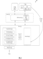
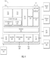
- FIG. 1 is a block diagram of a processing system 100 to support memory paging in virtualized systems using trust domains according to one embodiment.
- processing system 100 includes a virtualization server 110 that supports a number of client devices 101A-101C.
- the virtualization server 110 includes at least one processor 112 (also referred to as a processing device) that executes a trust domain resource manager (TDRM) 150.
- TDRM trust domain resource manager
- the TDRM 150 may be included as part virtual machine monitor (VMM) functionality.
- VMM also referred to as hypervisor
- hypervisor may refer to software, firmware, or hardware to create, run, and manage guest applications, such as a virtual machine (VM).
- the TDRM 150 may include a VMM that may instantiate one or more trust domains (TDs) 190A-190C (e.g., a software environment to execute a tenant (e.g., customer) workload) accessible by the client devices 101A-101C via a network interface 170.
- the client devices 101A-101C may include, but is not limited to, a desktop computer, a tablet computer, a laptop computer, a netbook, a notebook computer, a personal digital assistant (PDA), a server, a workstation, a cellular telephone, a mobile computing device, a smart phone, an Internet appliance or any other type of computing device.
- PDA personal digital assistant
- processor 112 implements a TD architecture and ISA extensions (TDX) for the TD architecture.
- the TD architecture provides isolation between TD workloads 190A-190C and from CSP software (e.g., TDRM 150 and/or a CSP VMM (e.g., root VMM 150)) executing on the processor 112).
- Components of the TD architecture can include 1) memory encryption via an MK-TME engine 145, 2) a resource management capability referred to herein as the TDRM 150, and 3) execution state and memory isolation capabilities in the processor 112 provided via a MOT 160 and via access-controlled TD control structures (i.e., TDCS 124 and TDTCS 128).
- the TDX architecture provides an ability of the processor 112 to deploy TDs 190A-190C that leverage the MK-TME engine 145, the MOT 160, and the access-controlled TD control structures (i.e., TDCS 124 and TDTCS 128) for secure operation of TDs 190A-190C.
- the processor 112 may include several components that include, but not limited to, one or more cores 120 (also referred to as processing cores 120), range registers 130 and a memory controller 140.
- the processor 112 may be used in a processing system 100 that is representative of processing systems based on the PENTIUM III TM , PENTIUM 4 TM , Xeon TM , Itanium, XScale TM and/or StrongARM TM microprocessing devices available from Intel Corporation of Santa Clara, California, although other systems (including PCs having other microprocessing devices, engineering workstations, set-top boxes and the like) may also be used.
- sample system 100 executes a version of the WINDOWS TM operating system available from Microsoft Corporation of Redmond, Washington, although other operating systems (UNIX and Linux for example), embedded software, and/or graphical user interfaces, may also be used.
- WINDOWS TM operating system available from Microsoft Corporation of Redmond, Washington, although other operating systems (UNIX and Linux for example), embedded software, and/or graphical user interfaces, may also be used.
- embodiments of the disclosure are not limited to any specific combination of hardware circuitry and software.
- processing core 120 may have a micro-architecture including processor logic and circuits.
- Processor cores 120 with different micro-architectures may share at least a portion of a common instruction set.
- similar register architectures may be implemented in different ways in different micro-architectures using various techniques, including dedicated physical registers, one or more dynamically allocated physical registers using a register renaming mechanism (e.g., the use of a register alias table (RAT), a reorder buffer (ROB) and a retirement register file).
- the processor core(s) 120 may execute instructions for the processor 112.
- the instructions may include, but are not limited to, pre-fetch logic to fetch instructions, decode logic to decode the instructions, execution logic to execute instructions and the like.
- the processor cores 120 include a cache (not shown) to cache instructions and/or data.
- the cache includes, but is not limited to, a level one, level two, and a last level cache (LLC), or any other configuration of the cache memory within the processor 112.
- Processing system 100 also includes a main memory 114 and a secondary storage 118 to store program binaries and other data.
- Data in the secondary storage 118 may be stored in blocks referred to as pages, and each page may correspond to a set of physical memory addresses.
- the virtualization server 110 may employ the TDRM/VMM 150 in which applications run by the core(s) 120, such as the TDs 190A-190C, use virtual memory addresses that are mapped to guest physical memory addresses, and guest physical memory addresses are mapped to host/system physical addresses by the memory controller 140.
- the core 120 may execute the memory controller 140 to load pages from the secondary storage 118 into the main memory 114 (which includes a volatile memory and/or a non-volatile memory) for faster access by software running on the processor 112 (e.g., on the core).
- the memory controller 140 When one of the TDs 190A-190C attempts to access a virtual memory address that corresponds to a physical memory address of a page loaded into the main memory 114, the memory controller 140 returns the requested data.
- the core 120 may execute the VMM portion of TDRM 150 to translate guest virtual addresses to host physical addresses of main memory 114, and provide parameters for a protocol that allows the core 120 to read, walk and interpret these mappings.
- a TD 190A may be created and launched by the TDRM 150.
- the TDRM 150 creates a TD 190A using a certain TD instruction.
- the TDRM 150 selects a 4KB aligned region of physical memory and provides this as a parameter to the TD create instruction. This region of memory is used as a TDCS 124 for the TD 190A.
- the TD instruction causes the processor 112 to verify that the destination 4KB page is assigned to the TD (using the MOT 160).
- the TD instruction further causes the processor 112 to generate an ephemeral memory encryption key and key ID for the TD 190A, and store the key ID in the TDCS 124.
- the TD architecture includes a MOT 160.
- the processor 112 consults the TDRM-managed MOT 160 to assign allocation of memory to TDs. This allows the TDRM 150 the full ability to manage memory as a resource without having any visibility into data resident in assigned TD memory.
- MOT 160 (which may be referred to as TD-MOT) is a structure, such as a table, managed by the processor 112 to enforce assignment of physical memory pages to executing TDs, such as TD 190A.
- the MOT 160 structure is used to hold meta-data attributes for each 4KB page of memory aligned with the TD 190A. ).
- the MOT 160 is aligned on a 4KB boundary of memory and occupies a physically contiguous region of memory protected from access by software after platform initialization.
- the MOT 160 is a micro-architectural structure and cannot be directly accessed by software.
- the MOT 160 holds the following security attributes for each 4KB page of host physical memory:
- the meta-data for each 4KB page of memory is directly indexed by a physical page address associated with the TD.
- a 4KB page referenced in the MOT 160 can belong to one running instance of a TD 190A.
- the processor 112 uses the MOT 160 to enforce that the physical addresses referenced by software operating as a tenant TD 190A or the TDRM 150 cannot access memory not explicitly assigned to it.
- the access control is enforced using the MOT 160 during the page walk for memory accesses made by software.
- Physical memory accesses performed by the processor 112 to memory that is not assigned to a tenant TD 190A or TDRM 150 fail with Abort page semantics.
- the MOT 160 enforces the following properties.
- TD 190A software outside a TD 190A should not be able to access (read/write/execute) in plain-text any memory belonging to a different TD (this includes TDRM 150).
- the TDRM 150 acts as a host and has full control of the cores 120 and other platform hardware.
- a TDRM 150 assigns software in a TD 190A-190C with logical processor(s). The TDRM 150, however, cannot access a TD's 190A-190C execution state on the assigned logical processor(s).
- a TDRM 150 assigns physical memory and I/O resources to the TDs 190A-190C, but is not privy to access the memory state of a TD 190A due to separate encryption keys, and other integrity and replay controls on memory.
- the processor 112 may utilize the MK-TME engine 145 to encrypt (and decrypt) memory used during execution.
- TME total memory encryption
- any memory accesses by software executing on the core 120 can be encrypted in memory with an encryption key.
- MK-TME is an enhancement to TME that allows use of multiple encryption keys (the number of supported keys is implementation dependent).
- the processor 112 may utilize the MK-TME engine 145 to cause different pages to be encrypted using different MK-TME keys.
- the MK-TME engine 145 may be utilized in the TD architecture described herein to support one or more encryption keys per each TD 190A-190C to help achieve the cryptographic isolation between different CSP customer workloads. For example, when MK-TME engine 145 is used in the TD architecture, the CPU enforces by default that TD (all pages) are to be encrypted using a TD-specific encryption key.
- Each TD 190A-190C may further choose specific TD memory pages to be plain text or encrypted.
- the TD memory pages may be encrypted using a combination of keys (e.g., ephemeral keys that are generated for each execution of the TD) that are unknown to the TDRM 150, and a binding ("tweak") operation.
- the binding operation binds the TD memory pages to a particular TD by using a host physical address (HPA) of the page as a parameter to an encryption algorithm which is utilized to encrypt the TD memory page. So if the TD memory page is moved to another location (e.g., in main memory 114 or secondary storage 118), the page cannot be decrypted correctly even if the TD-specific encryption key is used.
- HPA host physical address
- the TDRM 150 on occasion may need to perform a memory paging operations to reclaim memory pages allocated to a first TD by storing contents of the pages to a disk (e.g., an external hard disk). The freed memory page can then be allocated to a second TD that is in need of extra memory.
- Embodiments of the disclosure provide techniques to support full memory paging between different TDs in compute system 200 without losing any of its security properties (e.g., tamper resistant/detection and confidentiality on a per TD basis).
- processor 112 may implement a memory paging circuit 180.
- the memory paging circuit 180 allows the TDRM 150 to create a transportable page for a target TD memory page bound to a specific TD. This transportable page allows the TDRM 150 to page out the target TD memory page to use for another TD or a different location in memory.
- the memory paging circuit 180 may be implemented as part of the TDRM 150. In alternative implementations, the memory paging circuit 180 may be implemented in a separate hardware component, circuitry, dedicated logic, programmable logic, and microcode of the processor 112 or any combination thereof. In one implementation, the memory paging circuit 180 may include a micro-architecture including processor logic and circuits similar to the processing cores 120. In some implementations, the memory paging circuit 180 may include a dedicated portion of the same processor logic and circuits used by the processing cores 120.
- FIG. 2 illustrates a block diagram of an apparatus 200 including a data structure 201 according to one embodiment.
- apparatus 200 may be the same or similar to processing device 112.
- apparatus 200 includes the memory paging circuit 180 of the TDRM 150 of FIG. 1 , which implements processor instructions to support memory paging in virtualized systems using trust domains, such as TDs 190A and 190B.
- Each TD 190A and 190B is a software environment that can run VMMs, VMs, OSes, and/or applications.
- TD 190A is depicted as hosting VM 290A.
- the apparatus 200 provides isolation between workloads executed by each of the TDs 190A and 190B.
- each TD is cryptographically isolated in memory using at least one exclusive encryption key of the MK-TME engine 145 for encrypting the memory (holding code and/or data) associated with the trust domain.
- TD 190A may use encryption key 205A to encrypt TD memory page 203 of that TD
- TD 190B may use encryption key 205B to encrypt TD memory pages of TD 190D.
- Each TD may further choose specific TD memory pages to be plain text or encrypted using a combination of keys that are unknown to the TDRM 150 and a binding operation.
- the binding operation binds the TD memory page 203 to TD 190A by using a host physical address (HPA) 207 of the page as a parameter to an encryption algorithm which is utilized to encrypt the TD memory page 203.
- HPA host physical address
- the TDRM 150 may use the memory paging circuit 180 to page out a TD memory page 203 of TD 190A in order to provide memory to a different TD 190B.
- the TDRM 150 in accordance with the memory paging circuit 180 may execute an TD evict instruction 220 to evict the TD memory page 203 from the TD 190A.
- GKID e.g., Guest (TD) KeyID
- HKID e.g., Host KeyID
- the GKID are pages that are encrypted with TD's ephemeral key in which TDRM has the associated HKID and thus the encryption key pointer.
- the TDRM 150 marks in a paging table (not shown) that the TD memory page 203 is not available for TD 190A.
- the TDRM 150 marks the TD memory page 203 (e.g., in a paging table) as unavailable for the TD 190A.
- the TDRM 150 then flushes the page mappings of that page to the TD 190A, and any dirty cache lines for the page.
- a data structure 210 also referred to as a transportable page is created.
- the transportable page 210 allows the TDRM 150 to page out a TD memory page 203 in TD 190 for use for in TD 190B without losing any of the page's security properties.
- the transportable page 210 may include encrypted content that has been extracted from the TD memory page 203.
- the TDRM 150 copies the transportable page 210 to a secondary storage (e.g., file/disk). The TDRM 150 then invalidates cache lines for the old TD memory page 203 and makes the page available to a memory location associated with TD 190B.
- the TDRM 150 may store TD memory page 203 in a different location in memory 201. In such a case, the TDRM 150 may insert a TD memory page for a previously stored transportable page at the TD 190B.
- the TDRM 150 in accordance with the memory paging circuit 180 may execute a TD extract instruction 230.
- the TD extract instruction 230 first removes the binding that binds the TD memory page 203 a specific (HPA) memory location 207 associated with TD 190A.
- the TD extract instruction 230 may read the TD memory page 203 on behalf of the TD 190A. For example, the instruction may instruct the TD 190A to read the target TD memory page 203.
- TD extract instruction 230 when a TD memory page 203 is read in accordance with TD extract instruction 230, the contents of a TD-assigned volatile memory page are extracted from a source memory address of the page to a destination address of the transportable page 210.
- the TDRM 150 can use the TD extract instruction 230 to encrypt the transportable page 210 using the TD-specific encryption key 207A.
- the encrypted the transportable page 210 may include, but not limited to, a TDCS slot identifier 212, a HPA of the source TD memory page 214, a virtual address (VA) of a region (e.g., 128 byte) of memory where a cryptographic MAS is captured for the page content and meta-data, and a VA of a (4KB) page where the encrypted contents of the transportable page 210 are stored.
- the TDRM 150 may then instruct the apparatus 200 to transport the transportable page 210 to a different location in memory 201 or off to a storage device.
- the transportable page 210 may be saved with metadata that may include integrity value 219 for the page.
- the integrity value 219 may be a cryptographic hash value that is generated based on the contents of the page and the TD-specific encryption key 207A.
- the integrity value 219 can be generated using cryptographic hash algorithm, such as HMAC-SHA256, as the basis for data origin authentication and integrity verification. This integrity value 219 is used to verify that the transportable page 210 has not been tampered with on the storage device. For example, when the transportable page 210 is brought back to be inserted in memory 201, the TDRM 150 may check whether the integrity value 219 has changed in order to validate the contents of the transportable page 210.
- FIG. 3 illustrates is another example 300 of the apparatus 200 of FIG. 2 according to one embodiment.
- the TDRM 150 may insert contents of the memory page that was paged out of TD 190A.
- an application e.g., VM 290A
- the TDRM 150 takes the memory pages from disk and provides then back to any location in memory 210 associated with the TD 190A.
- the transportable page 210 is brought back to be inserted in memory, the TDRM 150 executes a TD insert page instruction 340.
- the TD insert page instruction 340 first removes the encryption of the transportable page 210. For example, the encrypted contents of transportable page 218 are decrypted based on the TD specific encryption key 205A. In one embodiment, the instruction performs an integrity validation operation on the decrypted contents of the transportable page 201 to ensure that the page has not been changed. To validate the transportable page 210, the instruction compares the integrity value 219 of the transportable page 210 to the integrity value 309 stored in memory of the TDRM 150. If the integrity validation 207 fails because the integrity values 219 and 309 do not match, the instruction may return an error notification to the TDRM 150 of a memory mapping failure associated with the TD 190A. If the integrity values 219 and 309 match, this indicates that the transportable page 210 has not been modified.
- the TDRM 150 then inserts the transportable page 210 at a HPA of a memory page 303 in memory 210.
- the TD insert page instruction 340 then instructs the TD 190A to bind the memory page 303 to TD 190A by using the ephemeral key associated with the TD 190A and specific HPA location 305.
- the specific HPA 303 may be passed to the TD 190A via the TD insert page instruction 340.
- the binding operation binds the memory page 303 back to TD 190A by using the HPA 305 as a parameter to an encryption algorithm which is utilized to encrypt the page 303.
- This binding allows the TD 190A to now correctly decrypt the content of the memory page 303, even though the page 303 may be at a different physical location from where it was paged out of the TD 190A assigned memory 201. As a result, the TD 190A may now correctly decrypt the contents of the TD memory page 303 because the encryption binds the page back to the TD 190A at the new memory location associated with the HPA 305.
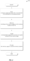
- FIG. 4 illustrates a flow diagram of a method 400 for supporting memory paging in virtualized systems using trust domains according to one embodiment.
- Method 400 may be performed by processing logic that may comprise hardware (e.g., circuitry, dedicated logic, programmable logic, microcode, etc.), software (such as instructions run on a processing device), firmware, or a combination thereof.
- the memory paging circuit 180 of processing device 100 in FIG. 1 may perform method 400.
- the illustrated implementations should be understood only as examples, and the illustrated processes can be performed in a different order, and some processes may be performed in parallel. Additionally, one or more processes can be omitted in various embodiments. Thus, not all processes are required in every implementation. Other process flows are possible.
- Method 400 begins at block 410 where a memory page 203 associated with a trust domain (TD) 190A executed by a processing device 112 is evicted.
- TD trust domain
- a binding 205A of the memory page 203 to a first memory location 207 of the TD is removed.
- a transportable page 210 that comprises encrypted contents 230 of the memory page 203 is created. Thereupon, the memory page 203 is provided to a second memory location 190B.
- FIG. 5A is a block diagram illustrating a micro-architecture for a processor 500 that implements techniques for supporting memory paging in virtualized systems using trust domains functionality in accordance with one embodiment of the disclosure.
- processor 500 depicts an in-order architecture core and a register renaming logic, out-of-order issue/execution logic to be included in a processor according to at least one embodiment of the disclosure.
- Processor 500 includes a front-end unit 530 coupled to an execution engine unit 550, and both are coupled to a memory unit 570.
- the processor 500 may include a reduced instruction set computing (RISC) core, a complex instruction set computing (CISC) core, a very long instruction word (VLIW) core, or a hybrid or alternative core type.
- processor 500 may include a special-purpose core, such as, for example, a network or communication core, compression engine, graphics core, or the like.
- processor 500 may be a multi-core processor or may part of a multi-processor system.
- the front end unit 530 includes a branch prediction unit 532 coupled to an instruction cache unit 534, which is coupled to an instruction translation lookaside buffer (TLB) 536, which is coupled to an instruction fetch unit 538, which is coupled to a decode unit 540.
- the decode unit 540 (also known as a decoder) may decode instructions, and generate as an output one or more micro-operations, micro-code entry points, microinstructions, other instructions, or other control signals, which are decoded from, or which otherwise reflect, or are derived from, the original instructions.
- the decoder 540 may be implemented using various different mechanisms.
- the instruction cache unit 534 is further coupled to the memory unit 570.
- the decode unit 540 is coupled to a rename/allocator unit 552 in the execution engine unit 550.
- the execution engine unit 550 includes the rename/allocator unit 552 coupled to a retirement unit 554 and a set of one or more scheduler unit(s) 556.
- the scheduler unit(s) 556 represents any number of different schedulers, including reservations stations (RS), central instruction window, etc.
- the scheduler unit(s) 556 is coupled to the physical register file(s) unit(s) 558.
- Each of the physical register file(s) units 558 represents one or more physical register files, different ones of which store one or more different data types, such as scalar integer, scalar floating point, packed integer, packed floating point, vector integer, vector floating point, etc., status (e.g., an instruction pointer that is the address of the next instruction to be executed), etc.
- the physical register file(s) unit(s) 558 is overlapped by the retirement unit 554 to illustrate various ways in which register renaming and out-of-order execution may be implemented (e.g., using a reorder buffer(s) and a retirement register file(s), using a future file(s), a history buffer(s), and a retirement register file(s); using a register maps and a pool of registers; etc.).
- the execution engine unit 550 may include for example a power management unit (PMU) 590 that governs power functions of the functional units.
- PMU power management unit
- the architectural registers are visible from the outside of the processor or from a programmer's perspective.
- the registers are not limited to any known particular type of circuit.
- Various different types of registers are suitable as long as they are capable of storing and providing data as described herein. Examples of suitable registers include, but are not limited to, dedicated physical registers, dynamically allocated physical registers using register renaming, combinations of dedicated and dynamically allocated physical registers, etc.
- the retirement unit 554 and the physical register file(s) unit(s) 558 are coupled to the execution cluster(s) 560.
- the execution cluster(s) 560 includes a set of one or more execution units 562 and a set of one or more memory access units 564.
- the execution units 562 may perform various operations (e.g., shifts, addition, subtraction, multiplication) and operate on various types of data (e.g., scalar floating point, packed integer, packed floating point, vector integer, vector floating point).
- While some embodiments may include a number of execution units dedicated to specific functions or sets of functions, other embodiments may include only one execution unit or multiple execution units that all perform all functions.
- the scheduler unit(s) 556, physical register file(s) unit(s) 558, and execution cluster(s) 560 are shown as being possibly plural because certain embodiments create separate pipelines for certain types of data/operations (e.g., a scalar integer pipeline, a scalar floating point/packed integer/packed floating point/vector integer/vector floating point pipeline, and/or a memory access pipeline that each have their own scheduler unit, physical register file(s) unit, and/or execution cluster - and in the case of a separate memory access pipeline, certain embodiments are implemented in which only the execution cluster of this pipeline has the memory access unit(s) 564). It should also be understood that where separate pipelines are used, one or more of these pipelines may be out-of-order issue/execution and the rest in-order.
- the set of memory access units 564 is coupled to the memory unit 570, which may include a data prefetcher 580, a data TLB unit 572, a data cache unit (DCU) 574, and a level 2 (L2) cache unit 576, to name a few examples.
- DCU 574 is also known as a first level data cache (L1 cache).
- L1 cache first level data cache
- the DCU 574 may handle multiple outstanding cache misses and continue to service incoming stores and loads. It also supports maintaining cache coherency.
- the data TLB unit 572 is a cache used to improve virtual address translation speed by mapping virtual and physical address spaces.
- the memory access units 564 may include a load unit, a store address unit, and a store data unit, each of which is coupled to the data TLB unit 572 in the memory unit 570.
- the L2 cache unit 576 may be coupled to one or more other levels of cache and eventually to a main memory.
- the data prefetcher 580 speculatively loads/prefetches data to the DCU 574 by automatically predicting which data a program is about to consume.
- Prefeteching may refer to transferring data stored in one memory location of a memory hierarchy (e.g., lower level caches or memory) to a higher-level memory location that is closer (e.g., yields lower access latency) to the processor before the data is actually demanded by the processor. More specifically, prefetching may refer to the early retrieval of data from one of the lower level caches/memory to a data cache and/or prefetch buffer before the processor issues a demand for the specific data being returned.
- processor 500 may be the same as processing device 100 described with respect to FIG. 1 to implement techniques for supporting memory paging in virtualized systems using trust domains with respect to implementations of the disclosure.
- the processor 500 may support one or more instructions sets (e.g., the x86 instruction set (with some extensions that have been added with newer versions); the MIPS instruction set of MIPS Technologies of Sunnyvale, CA; the ARM instruction set (with optional additional extensions such as NEON) of ARM Holdings of Sunnyvale, CA).
- the x86 instruction set (with some extensions that have been added with newer versions); the MIPS instruction set of MIPS Technologies of Sunnyvale, CA; the ARM instruction set (with optional additional extensions such as NEON) of ARM Holdings of Sunnyvale, CA).
- the core may support multithreading (executing two or more parallel sets of operations or threads), and may do so in a variety of ways including time sliced multithreading, simultaneous multithreading (where a single physical core provides a logical core for each of the threads that physical core is simultaneously multithreading), or a combination thereof (e.g., time sliced fetching and decoding and simultaneous multithreading thereafter such as in the Intel ® Hyperthreading technology).
- register renaming is described in the context of out-of-order execution, it should be understood that register renaming may be used in the in-order architecture.
- the illustrated embodiment of the processor also includes a separate instruction and data cache units and a shared L2 cache unit, alternative embodiments may have a single internal cache for both instructions and data, such as, for example, a Level 1 (L1) internal cache, or multiple levels of internal cache.
- the system may include a combination of an internal cache and an external cache that is external to the core and/or the processor. Alternatively, all of the cache may be external to the core and/or the processor.
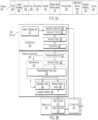
- FIG. 5B is a block diagram illustrating an in-order pipeline and a register renaming stage, out-of-order issue/execution pipeline implemented by processor 500 of FIG. 5A according to some embodiments of the disclosure.
- the solid lined boxes in FIG. 5B illustrate an in-order pipeline, while the dashed lined boxes illustrate a register renaming, out-of-order issue/execution pipeline.
- FIG. 5B illustrates an in-order pipeline, while the dashed lined boxes illustrate a register renaming, out-of-order issue/execution pipeline.
- a processor pipeline 501 includes a fetch stage 502, a length decode stage 504, a decode stage 506, an allocation stage 508, a renaming stage 510, a scheduling (also known as a dispatch or issue) stage 512, a register read/memory read stage 514, an execute stage 516, a write back/memory write stage 518, an exception handling stage 522, and a commit stage 524.
- the ordering of stages 502-524 may be different than illustrated and are not limited to the specific ordering shown in FIG. 5B .
- FIG. 6 illustrates a block diagram of the micro-architecture for a processor 600 that includes logic circuits to implement techniques for supporting data compression using match-scoring functionality in accordance with one embodiment of the disclosure.
- an instruction in accordance with one embodiment can be implemented to operate on data elements having sizes of byte, word, double word, quad word, etc., as well as data types, such as single and double precision integer and floating point datatypes.
- the in-order front end 601 is the part of the processor 600 that fetches instructions to be executed and prepares them to be used later in the processor pipeline.
- the front end 601 may include several units.
- the instruction prefetcher 626 fetches instructions from memory and feeds them to an instruction decoder 628, which in turn decodes or interprets them.
- the decoder decodes a received instruction into one or more operations called "micro-instructions" or “micro-operations” (also called micro op or uops) that the machine can execute.
- the decoder parses the instruction into an opcode and corresponding data and control fields that are used by the micro-architecture to perform operations in accordance with one embodiment.
- the trace cache 630 takes decoded uops and assembles them into program ordered sequences or traces in the uop queue 634 for execution.
- the microcode ROM 632 provides the uops needed to complete the operation.
- the trace cache 630 refers to an entry point programmable logic array (PLA) to determine a correct microinstruction pointer for reading the micro-code sequences to complete one or more instructions in accordance with one embodiment from the micro-code ROM 632.
- the out-of-order execution engine 603 is where the instructions are prepared for execution.
- the out-of-order execution logic has a number of buffers to smooth out and re-order the flow of instructions to optimize performance as they go down the pipeline and get scheduled for execution.
- the allocator logic allocates the machine buffers and resources that each uop needs in order to execute.
- the register renaming logic renames logic registers onto entries in a register file.
- the allocator also allocates an entry for each uop in one of the two uop queues, one for memory operations and one for non-memory operations, in front of the instruction schedulers: memory scheduler, fast scheduler 602, slow/general floating point scheduler 604, and simple floating point scheduler 606.
- the uop schedulers 602, 604, 606, determine when a uop is ready to execute based on the readiness of their dependent input register operand sources and the availability of the execution resources the uops need to complete their operation.
- the fast scheduler 602 of one embodiment can schedule on each half of the main clock cycle while the other schedulers can only schedule once per main processor clock cycle.
- the schedulers arbitrate for the dispatch ports to schedule uops for execution.
- Register files 608, 610 sit between the schedulers 602, 604, 606, and the execution units 612, 614, 616, 618, 620, 622, 624 in the execution block 611. There is a separate register file 608, 610, for integer and floating-point operations, respectively. Each register file 608, 610, of one embodiment also includes a bypass network that can bypass or forward just completed results that have not yet been written into the register file to new dependent uops. The integer register file 608 and the floating-point register file 610 are also capable of communicating data with the other. For one embodiment, the integer register file 608 is split into two separate register files, one register file for the low order 32 bits of data and a second register file for the high order 32 bits of data.
- the floating-point register file 610 of one embodiment has 128 bit wide entries because floating-point instructions typically have operands from 64 to 128 bits in width.
- the execution block 611 contains the execution units 612, 614, 616, 618, 620, 622, 624, where the instructions are actually executed.
- This section includes the register files 608, 610, that store the integer and floating point data operand values that the microinstructions need to execute.
- the processor 600 of one embodiment is comprised of a number of execution units: address generation unit (AGU) 612, AGU 614, fast ALU 616, fast ALU 618, slow ALU 620, floating point ALU 622, floating point move unit 624.
- AGU address generation unit
- the floating-point execution blocks 622, 624 execute floating point, MMX, SIMD, and SSE, or other operations.
- the floating point ALU 622 of one embodiment includes a 64 bit by 64 bit floating point divider to execute divide, square root, and remainder micro-ops. For embodiments of the disclosure, instructions involving a floating-point value may be handled with the floating-point hardware.
- the ALU operations go to the high-speed ALU execution units 616, 618.
- the fast ALUs 616, 618, of one embodiment can execute fast operations with an effective latency of half a clock cycle.
- most complex integer operations go to the slow ALU 620 as the slow ALU 620 includes integer execution hardware for long latency type of operations, such as a multiplier, shifts, flag logic, and branch processing.
- the AGUs 612, 614 executes memory load/store operations.
- the integer ALUs 616, 618, 620 are described in the context of performing integer operations on 64 bit data operands.
- the ALUs 616, 618, 620 can be implemented to support a variety of data bits including 16, 32, 128, 256, etc.
- the floating-point units 622, 624 can be implemented to support a range of operands having bits of various widths.
- the floating-point units 622, 624 can operate on 128 bits wide packed data operands in conjunction with SIMD and multimedia instructions.
- the uops schedulers 602, 604, 606, dispatch dependent operations before the parent load has finished executing.
- the processor 600 also includes logic to handle memory misses. If a data load misses in the data cache, there can be dependent operations in flight in the pipeline that have left the scheduler with temporarily incorrect data.
- a replay mechanism tracks and re-executes instructions that use incorrect data. Only the dependent operations need to be replayed and the independent ones are allowed to complete.
- the schedulers and replay mechanism of one embodiment of a processor are also designed to catch instruction sequences for text string comparison operations.
- the processor 600 also includes logic to implement memory paging in virtualized systems using trust domains according to embodiments of the disclosure.
- the execution block 611 of processor 600 may include memory paging circuit 180 of FIG. 1 , for implementing techniques for supporting memory paging in virtualized systems using trust domains functionality.
- processor 600 may be the processing device 100 of FIG. 1 .
- registers may refer to the on-board processor storage locations that are used as part of instructions to identify operands. In other words, registers may be those that are usable from the outside of the processor (from a programmer's perspective). However, the registers of an embodiment should not be limited in meaning to a particular type of circuit. Rather, a register of an embodiment is capable of storing and providing data, and performing the functions described herein.
- the registers described herein can be implemented by circuitry within a processor using any number of different techniques, such as dedicated physical registers, dynamically allocated physical registers using register renaming, combinations of dedicated and dynamically allocated physical registers, etc.
- integer registers store 32 bit integer data.
- a register file of one embodiment also may contain an eight multimedia SIMD register for packed data.
- the registers are understood to be data registers designed to hold packed data, such as 64 bits wide MMX TM registers (also referred to as 'mm' registers in some instances) in microprocessors enabled with MMX TM technology from Intel Corporation of Santa Clara, California. These MMX TM registers, available in both integer and floating point forms, can operate with packed data elements that accompany SIMD and SSE instructions. Similarly, 128 bits wide XMM TM registers relating to SSE2, SSE3, SSE4, or beyond (referred to generically as "SSEx”) technology can also be used to hold such packed data operands.
- SSEx 128 bits wide XMM TM registers relating to SSE2, SSE3, SSE4, or beyond
- the registers do not need to differentiate between the two data types.
- integer and floating point are either contained in the same register file or different register files.
- floating point and integer data may be stored in different registers or the same registers.
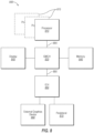
- multiprocessor system 700 is a point-to-point interconnect system, and includes a first processor 770 and a second processor 780 coupled via a point-to-point interconnect 750. While shown with only two processors 770, 780, it is to be understood that the scope of embodiments of the disclosure is not so limited. In other embodiments, one or more additional processors may be present in a given processor. In one embodiment, the multiprocessor system 700 may implement techniques for supporting memory paging in virtualized systems using trust domains functionality as described herein.
- Processors 770 and 780 are shown including integrated memory controller units 772 and 782, respectively.
- Processor 770 also includes as part of its bus controller units point-to-point (P-P) interfaces 776 and 778; similarly, second processor 780 includes P-P interfaces 786 and 788.
- Processors 770, 780 may exchange information via a point-to-point (P-P) interface 750 using P-P interface circuits 778, 788.
- IMCs 772 and 782 couple the processors to respective memories, namely a memory 732 and a memory 734, which may be portions of main memory locally attached to the respective processors.
- Processors 770, 780 may exchange information with a chipset 790 via individual P-P interfaces 752, 754 using point to point interface circuits 776, 794, 786, 798.
- Chipset 790 may also exchange information with a high-performance graphics circuit 738 via a high-performance graphics interface 739.
- a shared cache (not shown) may be included in either processor or outside of both processors, yet connected with the processors via P-P interconnect, such that either or both processors' local cache information may be stored in the shared cache if a processor is placed into a low power mode.
- first bus 716 may be a Peripheral Component Interconnect (PCI) bus, or a bus such as a PCI Express bus or another third generation I/O interconnect bus, although the scope of the disclosure is not so limited.
- PCI Peripheral Component Interconnect
- various I/O devices 714 may be coupled to first bus 716, along with a bus bridge 718 which couples first bus 716 to a second bus 720.
- second bus 720 may be a low pin count (LPC) bus.
- Various devices may be coupled to second bus 720 including, for example, a keyboard and/or mouse 722, communication devices 727 and a storage unit 728 such as a disk drive or other mass storage device which may include instructions/code and data 730, in one embodiment.
- an audio I/O 724 may be coupled to second bus 720.
- a system may implement a multi-drop bus or other such architecture.
- FIG. 8 shown is a block diagram of a system 800 in which one embodiment of the disclosure may operate.
- the system 800 may include one or more processors 810, 815, which are coupled to graphics memory controller hub (GMCH) 820.
- GMCH graphics memory controller hub
- processors 810, 815 implement techniques for supporting memory paging in virtualized systems using trust domains functionality according to embodiments of the disclosure.
- Each processor 810, 815 may be some version of the circuit, integrated circuit, processor, and/or silicon integrated circuit as described above. However, it should be noted that it is unlikely that integrated graphics logic and integrated memory control units would exist in the processors 810, 815.
- FIG. 8 illustrates that the GMCH 820 may be coupled to a memory 840 that may be, for example, a dynamic random access memory (DRAM).
- the DRAM may, for at least one embodiment, be associated with a non-volatile cache.
- the GMCH 820 may be a chipset, or a portion of a chipset.
- the GMCH 820 may communicate with the processor(s) 810, 815 and control interaction between the processor(s) 810, 815 and memory 840.
- the GMCH 820 may also act as an accelerated bus interface between the processor(s) 810, 815 and other elements of the system 800.
- the GMCH 820 communicates with the processor(s) 810, 815 via a multi-drop bus, such as a frontside bus (FSB) 895.
- a multi-drop bus such as a frontside bus (FSB) 895.
- GMCH 820 is coupled to a display 845 (such as a flat panel or touchscreen display).
- GMCH 820 may include an integrated graphics accelerator.
- GMCH 820 is further coupled to an input/output (I/O) controller hub (ICH) 850, which may be used to couple various peripheral devices to system 800.
- I/O controller hub ICH
- Shown for example in the embodiment of FIG. 8 is an external graphics device 860, which may be a discrete graphics device, coupled to ICH 850, along with another peripheral device 870.
- additional processor(s) 815 may include additional processors(s) that are the same as processor 810, additional processor(s) that are heterogeneous or asymmetric to processor 810, accelerators (such as, e.g., graphics accelerators or digital signal processing (DSP) units), field programmable gate arrays, or any other processor.
- accelerators such as, e.g., graphics accelerators or digital signal processing (DSP) units
- DSP digital signal processing
- FIG. 9 shown is a block diagram of a system 900 in which an embodiment of the disclosure may operate.
- FIG. 9 illustrates processors 970, 980.
- processors 970, 980 may techniques for supporting memory paging in virtualized systems using trust domains functionality as described above.
- Processors 970, 980 may include integrated memory and I/O control logic ("CL") 972 and 982, respectively and intercommunicate with each other via point-to-point interconnect 950 between point-to-point (P-P) interfaces 978 and 988 respectively.
- CL integrated memory and I/O control logic
- Processors 970, 980 each communicate with chipset 990 via point-to-point interconnects 952 and 954 through the respective P-P interfaces 976 to 994 and 986 to 998 as shown.
- the CL 972, 982 may include integrated memory controller units.
- CLs 972, 982 may include I/O control logic.
- memories 932, 934 coupled to CLs 972, 982 and I/O devices 914 are also coupled to the control logic 972, 982.
- Legacy I/O devices 915 are coupled to the chipset 990 via interface 996.
- FIG. 10 is a block diagram of a SoC 1000 in accordance with an embodiment of the disclosure. Dashed lined boxes are optional features on more advanced SoCs.
- an interconnect unit(s) 1012 is coupled to: an application processor 1020 which includes a set of one or more cores 1002A-N and shared cache unit(s) 1006; a system agent unit 1010; a bus controller unit(s) 1016; an integrated memory controller unit(s) 1014; a set of one or more media processors 1018 which may include integrated graphics logic 1008, an image processor 1024 for providing still and/or video camera functionality, an audio processor 1026 for providing hardware audio acceleration, and a video processor 1028 for providing video encode/decode acceleration; an static random access memory (SRAM) unit 1030; a direct memory access (DMA) unit 1032; and a display unit 1040 for coupling to one or more external displays.
- an application processor 1020 which includes a set of one or more cores 1002A-N and shared cache unit(s) 1006
- a memory module may be included in the integrated memory controller unit(s) 1014. In another embodiment, the memory module may be included in one or more other components of the SoC 1000 that may be used to access and/or control a memory.
- the application processor 1020 may include a PMU for implementing the memory paging circuit 180 as described in embodiments herein. In some embodiments, application processor 1020 may be the processing device 100 of FIG. 1 .
- the memory hierarchy includes one or more levels of cache within the cores, a set or one or more shared cache units 1006, and external memory (not shown) coupled to the set of integrated memory controller units 1014.
- the set of shared cache units 1006 may include one or more mid-level caches, such as level 2 (L2), level 3 (L3), level 4 (L4), or other levels of cache, a last level cache (LLC), and/or combinations thereof.
- the system agent 1010 includes those components coordinating and operating cores 1002A-N.
- the system agent unit 1010 may include for example a power control unit (PCU) and a display unit.
- the PCU may be or include logic and components needed for regulating the power state of the cores 1002A-N and the integrated graphics logic 1008.
- the display unit is for driving one or more externally connected displays.
- the cores 1002A-N may be homogeneous or heterogeneous in terms of architecture and/or instruction set. For example, some of the cores 1002A-N may be in order while others are out-of-order. As another example, two or more of the cores 1002A-N may be capable of execution the same instruction set, while others may be capable of executing only a subset of that instruction set or a different instruction set.
- the application processor 1020 may be a general-purpose processor, such as a Core TM i3, i5, i7, 2 Duo and Quad, Xeon TM , Itanium TM , Atom TM or Quark TM processor, which are available from Intel TM Corporation, of Santa Clara, Calif. Alternatively, the application processor 1020 may be from another company, such as ARM Holdings TM , Ltd, MIPS TM , etc.
- the application processor 1020 may be a special-purpose processor, such as, for example, a network or communication processor, compression engine, graphics processor, co-processor, embedded processor, or the like.
- the application processor 1020 may be implemented on one or more chips.
- the application processor 1020 may be a part of and/or may be implemented on one or more substrates using any of a number of process technologies, such as, for example, BiCMOS, CMOS, or NMOS.
- FIG. 11 is a block diagram of an embodiment of a system on-chip (SoC) design in accordance with the disclosure.
- SoC 1100 is included in user equipment (UE).
- UE refers to any device to be used by an end-user to communicate, such as a hand-held phone, smartphone, tablet, ultra-thin notebook, notebook with broadband adapter, or any other similar communication device.
- a UE connects to a base station or node, which potentially corresponds in nature to a mobile station (MS) in a GSM network.
- MS mobile station
- SOC 1100 includes 2 cores-1106 and 1107.
- Cores 1106 and 1107 may conform to an Instruction Set Architecture, such as an Intel ® Architecture Core TM -based processor, an Advanced Micro Devices, Inc. (AMD) processor, a MIPS-based processor, an ARM-based processor design, or a customer thereof, as well as their licensees or adopters.
- Cores 1106 and 1107 are coupled to cache control 1108 that is associated with bus interface unit 1109 and L2 cache 1110 to communicate with other parts of system 1100.
- Interconnect 1110 includes an on-chip interconnect, such as an IOSF, AMBA, or other interconnect discussed above, which potentially implements one or more aspects of the described disclosure.
- cores 1106, 1107 may implement techniques for supporting memory paging in virtualized systems using trust domains functionality as described in embodiments herein.
- Interconnect 1110 provides communication channels to the other components, such as a Subscriber Identity Module (SIM) 1130 to interface with a SIM card, a boot ROM 1140 to hold boot code for execution by cores 1106 and 1107 to initialize and boot SoC 1100, a SDRAM controller 1140 to interface with external memory (e.g. DRAM 1160), a flash controller 1145 to interface with non-volatile memory (e.g. Flash 1165), a peripheral control 1150 (e.g. Serial Peripheral Interface) to interface with peripherals, video codecs 1120 and Video interface 1125 to display and receive input (e.g. touch enabled input), GPU 1115 to perform graphics related computations, etc. Any of these interfaces may incorporate aspects of the disclosure described herein.
- the system 1100 illustrates peripherals for communication, such as a Bluetooth module 1170, 3G modem 1175, GPS 1180, and Wi-Fi 1185.
- FIG. 12 illustrates a diagrammatic representation of a machine in the example form of a computer system 1200 within which a set of instructions, for causing the machine to perform any one or more of the methodologies discussed herein, may be executed.
- the machine may be connected (e.g., networked) to other machines in a LAN, an intranet, an extranet, or the Internet.
- the machine may operate in the capacity of a server or a client device in a client-server network environment, or as a peer machine in a peer-to-peer (or distributed) network environment.
- the machine may be a personal computer (PC), a tablet PC, a set-top box (STB), a Personal Digital Assistant (PDA), a cellular telephone, a web appliance, a server, a network router, switch or bridge, or any machine capable of executing a set of instructions (sequential or otherwise) that specify actions to be taken by that machine.
- PC personal computer
- PDA Personal Digital Assistant
- STB set-top box
- WPA Personal Digital Assistant
- a cellular telephone a web appliance
- server a server
- network router switch or bridge
- the computer system 1200 includes a processing device 1202, a main memory 1204 (e.g., read-only memory (ROM), flash memory, dynamic random access memory (DRAM) (such as synchronous DRAM (SDRAM) or DRAM (RDRAM), etc.), a static memory 1206 (e.g., flash memory, static random access memory (SRAM), etc.), and a data storage device 1218, which communicate with each other via a bus 1230.
- main memory 1204 e.g., read-only memory (ROM), flash memory, dynamic random access memory (DRAM) (such as synchronous DRAM (SDRAM) or DRAM (RDRAM), etc.
- DRAM dynamic random access memory
- SDRAM synchronous DRAM
- RDRAM DRAM
- static memory 1206 e.g., flash memory, static random access memory (SRAM), etc.
- SRAM static random access memory
- Processing device 1202 represents one or more general-purpose processing devices such as a microprocessor, central processing unit, or the like. More particularly, the processing device may be complex instruction set computing (CISC) microprocessor, reduced instruction set computer (RISC) microprocessor, very long instruction word (VLIW) microprocessor, or processor implementing other instruction sets, or processors implementing a combination of instruction sets. Processing device 1202 may also be one or more special-purpose processing devices such as an application-specific integrated circuit (ASIC), a field programmable gate array (FPGA), a digital signal processor (DSP), network processor, or the like. In one embodiment, processing device 1202 may include one or more processing cores. The processing device 1202 is configured to execute the processing logic 1226 for performing the operations and steps discussed herein. In one embodiment, processing device 1202 is the same as processor architecture 100 described with respect to FIG. 1 that implements techniques for supporting memory paging in virtualized systems using trust domains functionality as described herein with embodiments of the disclosure.
- CISC complex instruction set computing
- the computer system 1200 may further include a network interface device 1208 communicably coupled to a network 1220.
- the computer system 1200 also may include a video display unit 1210 (e.g., a liquid crystal display (LCD) or a cathode ray tube (CRT)), an alphanumeric input device 1212 (e.g., a keyboard), a cursor control device 1214 (e.g., a mouse), and a signal generation device 1216 (e.g., a speaker).
- video display unit 1210 e.g., a liquid crystal display (LCD) or a cathode ray tube (CRT)
- an alphanumeric input device 1212 e.g., a keyboard
- a cursor control device 1214 e.g., a mouse
- signal generation device 1216 e.g., a speaker
- computer system 1200 may include a graphics processing unit 1222, a video processing unit 1228, and an audio processing unit 1232.
- the data storage device 1218 may include a non-transitory machine-accessible storage medium 1224 on which is stored software 1226 implementing any one or more of the methodologies of functions described herein, such as implementing memory paging in virtualized systems using trust domains on threads in a processing device, such as processing device 100 of FIG. 1 , as described above.
- the software 1226 may also reside, completely or at least partially, within the main memory 1204 as instructions 1226 and/or within the processing device 1202 as processing logic 1226 during execution thereof by the computer system 1200; the main memory 1204 and the processing device 1202 also constituting machine-accessible storage media.
- the non-transitory machine-readable storage medium 1224 may also be used to store instructions 1226 implementing the memory paging circuit 180 on threads in a processing device such as described with respect to processing device 100 in FIG. 1 , and/or a software library containing methods that call the above applications. While the non-transitory machine-accessible storage medium 1224 is shown in an example embodiment to be a single medium, the term "machine-accessible storage medium" should be taken to include a single medium or multiple media (e.g., a centralized or distributed database, and/or associated caches and servers) that store the one or more sets of instructions.
- machine-accessible storage medium shall also be taken to include any medium that is capable of storing, encoding or carrying a set of instruction for execution by the machine and that cause the machine to perform any one or more of the methodologies of the disclosure.
- machine-accessible storage medium shall accordingly be taken to include, but not be limited to, solid-state memories, and optical and magnetic media.
- a design may go through various stages, from creation to simulation to fabrication.
- Data representing a design may represent the design in a number of manners.
- the hardware may be represented using a hardware description language or another functional description language.
- a circuit level model with logic and/or transistor gates may be produced at some stages of the design process.
- most designs, at some stage reach a level of data representing the physical placement of various devices in the hardware model.
- the data representing the hardware model may be the data specifying the presence or absence of various features on different mask layers for masks used to produce the integrated circuit.
- the data may be stored in any form of a machine readable medium.
- a memory or a magnetic or optical storage such as a disc may be the machine readable medium to store information transmitted via optical or electrical wave modulated or otherwise generated to transmit such information.
- an electrical carrier wave indicating or carrying the code or design is transmitted, to the extent that copying, buffering, or re-transmission of the electrical signal is performed, a new copy is made.
- a communication provider or a network provider may store on a tangible, machine-readable medium, at least temporarily, an article, such as information encoded into a carrier wave, embodying techniques of embodiments of the disclosure.
- a module as used herein refers to any combination of hardware, software, and/or firmware.
- a module includes hardware, such as a micro-controller, associated with a non-transitory medium to store code adapted to be executed by the micro-controller. Therefore, reference to a module, in one embodiment, refers to the hardware, which is specifically configured to recognize and/or execute the code to be held on a non-transitory medium.
- use of a module refers to the non-transitory medium including the code, which is specifically adapted to be executed by the microcontroller to perform predetermined operations.
- the term module in this example may refer to the combination of the microcontroller and the non-transitory medium.
- a first and a second module may share hardware, software, firmware, or a combination thereof, while potentially retaining some independent hardware, software, or firmware.
- use of the term logic includes hardware, such as transistors, registers, or other hardware, such as programmable logic devices.
- phrase 'configured to,' in one embodiment refers to arranging, putting together, manufacturing, offering to sell, importing and/or designing an apparatus, hardware, logic, or element to perform a designated or determined task.
- an apparatus or element thereof that is not operating is still 'configured to' perform a designated task if it is designed, coupled, and/or interconnected to perform said designated task.
- a logic gate may provide a 0 or a 1 during operation.
- a logic gate 'configured to' provide an enable signal to a clock does not include every logic gate that may provide a 1 or 0. Instead, the logic gate is one coupled in some manner that during operation the 1 or 0 output is to enable the clock.
- use of the phrases 'to,' 'capable of/to,' and/or 'operable to,' in one embodiment refers to some apparatus, logic, hardware, and/or element designed in such a way to enable use of the apparatus, logic, hardware, and/or element in a specified manner.
- use of, capable to, or operable to, in one embodiment refers to the latent state of an apparatus, logic, hardware, and/or element, where the apparatus, logic, hardware, and/or element is not operating but is designed in such a manner to enable use of an apparatus in a specified manner.
- a value includes any known representation of a number, a state, a logical state, or a binary logical state. Often, the use of logic levels, logic values, or logical values is also referred to as 1's and 0's, which simply represents binary logic states. For example, a 1 refers to a high logic level and 0 refers to a low logic level.
- a storage cell such as a transistor or flash cell, may be capable of holding a single logical value or multiple logical values.
- the decimal number ten may also be represented as a binary value of 910 and a hexadecimal letter A. Therefore, a value includes any representation of information capable of being held in a computer system.
- values or portions of values may represent states.
- a first value such as a logical one
- a second value such as a logical zero
- reset and set refer to a default and an updated value or state, respectively.
- a default value potentially includes a high logical value, i.e. reset
- an updated value potentially includes a low logical value, i.e. set.
- any combination of values may be utilized to represent any number of states.
- a non-transitory machine-accessible/readable medium includes any mechanism that provides (i.e., stores and/or transmits) information in a form readable by a machine, such as a computer or electronic system.
- a non-transitory machine-accessible medium includes random-access memory (RAM), such as static RAM (SRAM) or dynamic RAM (DRAM); ROM; magnetic or optical storage medium; flash memory devices; electrical storage devices; optical storage devices; acoustical storage devices; other form of storage devices for holding information received from transitory (propagated) signals (e.g., carrier waves, infrared signals, digital signals); etc., which are to be distinguished from the non-transitory mediums that may receive information there from.
- RAM random-access memory
- SRAM static RAM
- DRAM dynamic RAM
- a machine-readable medium may include any mechanism for storing or transmitting information in a form readable by a machine (e.g., a computer), but is not limited to, floppy diskettes, optical disks, Compact Disc, Read-Only Memory (CD-ROMs), and magnetooptical disks, Read-Only Memory (ROMs), Random Access Memory (RAM), Erasable Programmable Read-Only Memory (EPROM), Electrically Erasable Programmable Read-Only Memory (EEPROM), magnetic or optical cards, flash memory, or a tangible, machine-readable storage used in the transmission of information over the Internet via electrical, optical, acoustical or other forms of propagated signals (e.g., carrier waves, infrared signals, digital signals, etc.). Accordingly, the computer-readable signals
Landscapes
- Engineering & Computer Science (AREA)
- Theoretical Computer Science (AREA)
- General Physics & Mathematics (AREA)
- General Engineering & Computer Science (AREA)
- Physics & Mathematics (AREA)
- Computer Security & Cryptography (AREA)
- Computer Hardware Design (AREA)
- Software Systems (AREA)
- General Health & Medical Sciences (AREA)
- Bioethics (AREA)
- Health & Medical Sciences (AREA)
- Databases & Information Systems (AREA)
- Storage Device Security (AREA)
- Memory System Of A Hierarchy Structure (AREA)
Claims (17)
- Verarbeitungsvorrichtung (112), umfassend:eine Speichersteuerung (140), undeine Speicher-Paging-Schaltung (180), die betreibbar mit der Speichersteuerung (140) gekoppelt ist, um:eine transportierbare Seite (210) in einen Speicherort einzufügen, der einer Vertrauensdomäne, TD, (180A) zugeordnet ist, die von der Verarbeitungsvorrichtung (112) ausgeführt wird, wobei die transportierbare Seite (210) verschlüsselten Inhalt einer ersten Speicherseite der TD (190A) umfasst, wobei der verschlüsselte Inhalt eine physische Adresse (214) der ersten Speicherseite und/oder eine virtuelle Adresse (218) einer zweiten Speicherseite umfasst, auf der der verschlüsselte Inhalt der transportierbaren Seite (210) gespeichert ist, und mit einem Schlüssel (205A) verschlüsselt wird, der der TD (190A) zugeordnet ist, wobei die TD (190A) im Speicher (201) unter Verwendung des Schlüssels (205A) zum Verschlüsseln des der TD (190A) zugeordneten Speichers (201) kryptografisch isoliert ist;eine dritte Speicherseite (303), die der TD (190A) zugeordnet ist, durch Binden der transportierbaren Seite (210) an die TD (190A) zu erzeugen, wobei das Binden der transportierbaren Seite (210) an die TD (190A) das Entschlüsseln des Inhalts der transportierbaren Seite (210) unter Verwendung des TD-spezifischen Verschlüsselungsschlüssels (205A), und erneutes Verschlüsseln des Inhalts der transportierbaren Seite (210) auf der Grundlage eines temporären Schlüssels, der der TD (190A) zugeordnet ist, und einer physischen Adresse des Speicherorts umfasst, wobei der temporäre Schlüssel für jede Ausführung der TD generiert wird; und auf den Inhalt der dritten Speicherseite (303) durch Entschlüsseln des Inhalts der dritten Speicherseite unter Verwendung des temporären Schlüssels, der der TD (190A) zugeordnet ist, und der physischen Adresse des Speicherorts zuzugreifen.
- Verarbeitungsvorrichtung (112) nach Anspruch 1, wobei die TD (190A) eine kryptografisch geschützte Ausführungsumgebung ist.
- Verarbeitungsvorrichtung (112) nach Anspruch 1 oder 2, wobei zum Einfügen der transportierbaren Seite (210) in den Speicherort die Speicher-Paging-Schaltung (180) ferner:den Inhalt der transportierbaren Seite (210) unter Verwendung des Schlüssels (205A), der der TD (190A) zugeordnet ist, entschlüsseln soll; undden entschlüsselten Inhalt der transportierbaren Seite (210) verifizieren soll.
- Verarbeitungsvorrichtung (112) nach Anspruch 3, wobei, um den entschlüsselten Inhalt zu verifizieren, der Speicher-Paging-Schaltkreis (180) ferner:
bestimmen soll, ob ein erster im Speicher gespeicherter Integritätswert (201) mit einem zweiten Integritätswert übereinstimmt, der von der transportierbaren Seite (210) abgeleitet wird. - Verarbeitungsvorrichtung (112) nach Anspruch 3 oder 4, wobei als Reaktion auf das Erkennen, dass die entschlüsselten Inhalte nicht überprüft werden, die Verarbeitungsschaltung (112) ferner:
eine Warnung generieren soll, die einen Speicher-Paging-Fehler angibt, der der TD (190A) zugeordnet ist. - Verarbeitungsvorrichtung (112) nach einem der Ansprüche 1-5, wobei der Speicherort eine physische Host-Adresse (305) aufweist, die der TD (190A) zugeordnet ist.
- Verarbeitungsvorrichtung (112) nach einem der Ansprüche 1-6, wobei die Verarbeitungsschaltung (112) ferner:die dritte Speicherseite (303), die der TD (190A) zugeordnet ist, räumen soll;ein Binden der dritten Speicherseite (303) zu dem Speicherort der TD (190A) entfernen soll; unddie transportierbare Seite (210), die den verschlüsselten Inhalt der dritten Speicherseite (303) umfasst, erzeugen soll.
- Verfahren, umfassend:Einfügen einer transportierbaren Seite (210) in einen Speicherort, der einer Vertrauensdomäne TD (190A), zugeordnet ist, ausgeführt durch eine Verarbeitungsvorrichtung (112), wobei die transportierbare Seite (210) verschlüsselten Inhalt einer ersten Speicherseite der TD (190A) umfasst, wobei der verschlüsselte Inhalt eine physische Adresse (214) der ersten Speicherseite und/oder eine virtuelle Adresse (218) einer zweiten Speicherseite umfasst, auf der der verschlüsselte Inhalt der transportierbaren Seite (210) gespeichert ist, und unter Verwendung eines Schlüssels (205A) verschlüsselt wird, der der TD (190A) zugeordnet ist, wobei die TD (190A) im Speicher (201) unter Verwendung des Schlüssels (205A) zum Verschlüsseln des Speichers (201), der der TD zugeordnet ist, kryptografisch isoliert ist;Erzeugen einer dritten Speicherseite (303), die der TD (190A) zugeordnet ist, durch Binden der transportierbaren Seite (210) an die TD (190A), wobei das Binden der transportierbaren Seite (210) an die TD (190A) das Entschlüsseln des Inhalts der transportierbaren Seite (210) unter Verwendung des TD-spezifischen Verschlüsselungsschlüssel (205A) umfasst, underneutes Verschlüsseln des Inhalts der transportierbaren Seite (210) auf der Grundlage eines temporären Schlüssels, der der TD (190A) zugeordnet ist, und einer physischen Adresse des Speicherorts, wobei der temporäre Schlüssel für jede Ausführung der TD generiert wird; und Zugreifen auf den Inhalt der dritten Speicherseite (303) durch Entschlüsseln des Inhalts der dritten Speicherseite unter Verwendung des temporären Schlüssels, der der TD (190A) und der physischen Adresse des Speicherorts zugeordnet ist.
- Verfahren nach Anspruch 8, wobei die TD (190A) eine kryptografisch geschützte Ausführungsumgebung ist.
- Verfahren nach Anspruch 8 oder 9, wobei das Einfügen der transportierbaren Seite (210) in den Speicherort ferner umfasst:Entschlüsseln des Inhalts der transportierbaren Seite (210) unter Verwendung des Schlüssels (205A), der der TD (190A) zugeordnet ist; undVerifizieren des entschlüsselten Inhalts der transportierbaren Seite (210).
- Verfahren nach Anspruch 10, wobei das Verifizieren der entschlüsselten Inhalte ferner umfasst:
Bestimmen, ob ein erster im Speicher (201) gespeicherter Integritätswert mit einem zweiten Integritätswert übereinstimmt, der von der transportierbaren Seite (210) abgeleitet wird. - Verfahren nach Anspruch 10 oder 11, ferner umfassend:
als Reaktion auf das Erkennen, dass der entschlüsselte Inhalt nicht verifiziert ist, Generieren einer Warnung, die einen der TD (190A) zugeordneten Speicher-Paging-Fehler angibt. - Verfahren nach einem der Ansprüche 8-12, wobei der Speicherort eine physische Host-Adresse (305) aufweist, die der TD (190A) zugeordnet ist.
- Verfahren nach einem der Ansprüche 8-13, ferner umfassend:Räumen der dritten Speicherseite (303), die der TD zugeordnet ist (190A);Entfernen eines Bindens der dritten Speicherseite an den Speicherort der TD (190A); undErzeugen der transportierbaren Seite (210), die den verschlüsselten Inhalt der dritten Speicherseite (303) umfasst.
- System, umfassend:einen Speicher (201), um eine Vertrauensdomäne (190) zu speichern; undeine Verarbeitungsvorrichtung (112) nach einem der Ansprüche 1-7, die betreibbar mit dem Speicher (201) gekoppelt ist.
- Computerprogrammprodukt, das Anweisungen umfasst, die, wenn das Programm von einer Verarbeitungsvorrichtung ausgeführt wird, die Verarbeitungsvorrichtung veranlassen, das Verfahren nach einem der Ansprüche 8-14 durchzuführen.
- Computerlesbares Speichermedium, auf dem das Computerprogrammprodukt nach Anspruch 16 gespeichert ist.
Priority Applications (1)
| Application Number | Priority Date | Filing Date | Title |
|---|---|---|---|
| EP25156532.1A EP4560481A3 (de) | 2018-03-29 | 2019-02-26 | Unterstützung von speicherfunkruf in virtualisierten systemen mit vertrauensdomänen |
Applications Claiming Priority (2)
| Application Number | Priority Date | Filing Date | Title |
|---|---|---|---|
| US15/940,490 US10649911B2 (en) | 2018-03-29 | 2018-03-29 | Supporting memory paging in virtualized systems using trust domains |
| EP19159537.0A EP3547200B1 (de) | 2018-03-29 | 2019-02-26 | Unterstützung von speicher-paging in virtualisierten systemen unter verwendung von vertrauensdomänen |
Related Parent Applications (2)
| Application Number | Title | Priority Date | Filing Date |
|---|---|---|---|
| EP19159537.0A Division-Into EP3547200B1 (de) | 2018-03-29 | 2019-02-26 | Unterstützung von speicher-paging in virtualisierten systemen unter verwendung von vertrauensdomänen |
| EP19159537.0A Division EP3547200B1 (de) | 2018-03-29 | 2019-02-26 | Unterstützung von speicher-paging in virtualisierten systemen unter verwendung von vertrauensdomänen |
Related Child Applications (1)
| Application Number | Title | Priority Date | Filing Date |
|---|---|---|---|
| EP25156532.1A Division EP4560481A3 (de) | 2018-03-29 | 2019-02-26 | Unterstützung von speicherfunkruf in virtualisierten systemen mit vertrauensdomänen |
Publications (2)
| Publication Number | Publication Date |
|---|---|
| EP4002178A1 EP4002178A1 (de) | 2022-05-25 |
| EP4002178B1 true EP4002178B1 (de) | 2025-02-12 |
Family
ID=65229693
Family Applications (3)
| Application Number | Title | Priority Date | Filing Date |
|---|---|---|---|
| EP19159537.0A Active EP3547200B1 (de) | 2018-03-29 | 2019-02-26 | Unterstützung von speicher-paging in virtualisierten systemen unter verwendung von vertrauensdomänen |
| EP22151703.0A Active EP4002178B1 (de) | 2018-03-29 | 2019-02-26 | Unterstützung von speicher-paging in virtualisierten systemen unter verwendung von vertrauensdomänen |
| EP25156532.1A Pending EP4560481A3 (de) | 2018-03-29 | 2019-02-26 | Unterstützung von speicherfunkruf in virtualisierten systemen mit vertrauensdomänen |
Family Applications Before (1)
| Application Number | Title | Priority Date | Filing Date |
|---|---|---|---|
| EP19159537.0A Active EP3547200B1 (de) | 2018-03-29 | 2019-02-26 | Unterstützung von speicher-paging in virtualisierten systemen unter verwendung von vertrauensdomänen |
Family Applications After (1)
| Application Number | Title | Priority Date | Filing Date |
|---|---|---|---|
| EP25156532.1A Pending EP4560481A3 (de) | 2018-03-29 | 2019-02-26 | Unterstützung von speicherfunkruf in virtualisierten systemen mit vertrauensdomänen |
Country Status (3)
| Country | Link |
|---|---|
| US (3) | US10649911B2 (de) |
| EP (3) | EP3547200B1 (de) |
| CN (2) | CN120493303A (de) |
Families Citing this family (6)
| Publication number | Priority date | Publication date | Assignee | Title |
|---|---|---|---|---|
| US10628315B2 (en) | 2017-09-28 | 2020-04-21 | Intel Corporation | Secure memory repartitioning technologies |
| US10649911B2 (en) * | 2018-03-29 | 2020-05-12 | Intel Corporation | Supporting memory paging in virtualized systems using trust domains |
| US10521149B2 (en) * | 2018-05-30 | 2019-12-31 | Red Hat, Inc. | Memory poisoning support for free page hinting |
| US11328111B2 (en) | 2020-09-25 | 2022-05-10 | Intel Corporation | Broadcast remote sealing for scalable trusted execution environment provisioning |
| US12353520B2 (en) * | 2020-11-02 | 2025-07-08 | Intel Corporation | Graphics security with synergistic encryption, content-based and resource management technology |
| US12248807B2 (en) | 2020-12-26 | 2025-03-11 | Intel Corporation | Methods, apparatus, systems, and instructions to migrate protected virtual machines |
Family Cites Families (18)
| Publication number | Priority date | Publication date | Assignee | Title |
|---|---|---|---|---|
| US6986052B1 (en) * | 2000-06-30 | 2006-01-10 | Intel Corporation | Method and apparatus for secure execution using a secure memory partition |
| US8468244B2 (en) * | 2007-01-05 | 2013-06-18 | Digital Doors, Inc. | Digital information infrastructure and method for security designated data and with granular data stores |
| US9195846B2 (en) * | 2008-10-01 | 2015-11-24 | Hewlett-Packard Development Company, L.P. | Access grants |
| US20100228961A1 (en) * | 2009-03-03 | 2010-09-09 | Erf Wireless, Inc. | Hierarchical secure networks |
| US8799673B2 (en) * | 2009-12-31 | 2014-08-05 | Intel Corporation | Seamlessly encrypting memory regions to protect against hardware-based attacks |
| US8812871B2 (en) * | 2010-05-27 | 2014-08-19 | Cisco Technology, Inc. | Method and apparatus for trusted execution in infrastructure as a service cloud environments |
| US9430384B2 (en) * | 2013-03-31 | 2016-08-30 | Intel Corporation | Instructions and logic to provide advanced paging capabilities for secure enclave page caches |
| US9747028B1 (en) * | 2013-12-13 | 2017-08-29 | Amazon Technologies, Inc. | Artificial memory pressure for low memory machine |
| US9697140B2 (en) * | 2014-09-23 | 2017-07-04 | Intel Corporation | Encryption integrity check with CRC encryption in memory using a word count- and address-derived nonce |
| US9684608B2 (en) | 2014-10-28 | 2017-06-20 | Intel Corporation | Maintaining a secure processing environment across power cycles |
| US9893881B2 (en) * | 2015-06-29 | 2018-02-13 | Intel Corporation | Efficient sharing of hardware encryption pipeline for multiple security solutions |
| US10255191B2 (en) * | 2015-08-13 | 2019-04-09 | Advanced Micro Devices, Inc. | Logical memory address regions |
| US9678687B2 (en) * | 2015-09-25 | 2017-06-13 | Mcafee, Inc. | User mode heap swapping |
| US9990249B2 (en) | 2015-12-24 | 2018-06-05 | Intel Corporation | Memory integrity with error detection and correction |
| US10810321B2 (en) | 2016-08-11 | 2020-10-20 | Intel Corporation | Secure public cloud |
| US10675103B2 (en) * | 2016-08-16 | 2020-06-09 | Ethicon Llc | Robotics communication and control |
| US20180373646A1 (en) * | 2017-06-22 | 2018-12-27 | Technion Research & Development Foundation Ltd | Cache unit useful for secure execution |
| US10649911B2 (en) * | 2018-03-29 | 2020-05-12 | Intel Corporation | Supporting memory paging in virtualized systems using trust domains |
-
2018
- 2018-03-29 US US15/940,490 patent/US10649911B2/en active Active
-
2019
- 2019-02-26 EP EP19159537.0A patent/EP3547200B1/de active Active
- 2019-02-26 EP EP22151703.0A patent/EP4002178B1/de active Active
- 2019-02-26 EP EP25156532.1A patent/EP4560481A3/de active Pending
- 2019-02-28 CN CN202510564841.3A patent/CN120493303A/zh active Pending
- 2019-02-28 CN CN201910149638.4A patent/CN110321729A/zh active Pending
-
2020
- 2020-03-26 US US16/831,381 patent/US11288206B2/en active Active
-
2022
- 2022-03-28 US US17/706,396 patent/US20220214976A1/en not_active Abandoned
Also Published As
| Publication number | Publication date |
|---|---|
| EP4560481A3 (de) | 2025-08-06 |
| EP3547200B1 (de) | 2022-03-16 |
| EP4560481A2 (de) | 2025-05-28 |
| CN110321729A (zh) | 2019-10-11 |
| CN120493303A (zh) | 2025-08-15 |
| US10649911B2 (en) | 2020-05-12 |
| US20190042466A1 (en) | 2019-02-07 |
| US20220214976A1 (en) | 2022-07-07 |
| US11288206B2 (en) | 2022-03-29 |
| EP4002178A1 (de) | 2022-05-25 |
| EP3547200A1 (de) | 2019-10-02 |
| US20200226071A1 (en) | 2020-07-16 |
Similar Documents
| Publication | Publication Date | Title |
|---|---|---|
| KR102886909B1 (ko) | 신뢰 도메인들을 사용한 가상화된 시스템들에서의 격리 제공 | |
| US12254341B2 (en) | Scalable virtual machine operation inside trust domains within the trust domain architecture | |
| US11829517B2 (en) | Method and apparatus for trust domain creation and destruction | |
| US9942035B2 (en) | Platform migration of secure enclaves | |
| EP3757847B1 (de) | Verhinderung von trust-domain-zugriff unter verwendung von speichereigentumsbits in bezug auf cache-zeilen | |
| US20220214976A1 (en) | Supporting memory paging in virtualized systems using trust domains | |
| US12174972B2 (en) | Secure encryption key management in trust domains | |
| US20190095345A1 (en) | Evicting clean secure pages without encryption | |
| US10324862B2 (en) | Supporting oversubscription of guest enclave memory pages |
Legal Events
| Date | Code | Title | Description |
|---|---|---|---|
| PUAI | Public reference made under article 153(3) epc to a published international application that has entered the european phase |
Free format text: ORIGINAL CODE: 0009012 |
|
| STAA | Information on the status of an ep patent application or granted ep patent |
Free format text: STATUS: THE APPLICATION HAS BEEN PUBLISHED |
|
| AC | Divisional application: reference to earlier application |
Ref document number: 3547200 Country of ref document: EP Kind code of ref document: P |
|
| AK | Designated contracting states |
Kind code of ref document: A1 Designated state(s): AL AT BE BG CH CY CZ DE DK EE ES FI FR GB GR HR HU IE IS IT LI LT LU LV MC MK MT NL NO PL PT RO RS SE SI SK SM TR |
|
| STAA | Information on the status of an ep patent application or granted ep patent |
Free format text: STATUS: REQUEST FOR EXAMINATION WAS MADE |
|
| 17P | Request for examination filed |
Effective date: 20221122 |
|
| RBV | Designated contracting states (corrected) |
Designated state(s): AL AT BE BG CH CY CZ DE DK EE ES FI FR GB GR HR HU IE IS IT LI LT LU LV MC MK MT NL NO PL PT RO RS SE SI SK SM TR |
|
| GRAP | Despatch of communication of intention to grant a patent |
Free format text: ORIGINAL CODE: EPIDOSNIGR1 |
|
| STAA | Information on the status of an ep patent application or granted ep patent |
Free format text: STATUS: GRANT OF PATENT IS INTENDED |
|
| INTG | Intention to grant announced |
Effective date: 20240910 |
|
| GRAS | Grant fee paid |
Free format text: ORIGINAL CODE: EPIDOSNIGR3 |
|
| GRAA | (expected) grant |
Free format text: ORIGINAL CODE: 0009210 |
|
| STAA | Information on the status of an ep patent application or granted ep patent |
Free format text: STATUS: THE PATENT HAS BEEN GRANTED |
|
| AC | Divisional application: reference to earlier application |
Ref document number: 3547200 Country of ref document: EP Kind code of ref document: P |
|
| AK | Designated contracting states |
Kind code of ref document: B1 Designated state(s): AL AT BE BG CH CY CZ DE DK EE ES FI FR GB GR HR HU IE IS IT LI LT LU LV MC MK MT NL NO PL PT RO RS SE SI SK SM TR |
|
| REG | Reference to a national code |
Ref country code: GB Ref legal event code: FG4D |
|
| REG | Reference to a national code |
Ref country code: CH Ref legal event code: EP |
|
| REG | Reference to a national code |
Ref country code: DE Ref legal event code: R096 Ref document number: 602019066019 Country of ref document: DE |
|
| REG | Reference to a national code |
Ref country code: IE Ref legal event code: FG4D |
|
| P01 | Opt-out of the competence of the unified patent court (upc) registered |
Free format text: CASE NUMBER: APP_6517/2025 Effective date: 20250207 |
|
| REG | Reference to a national code |
Ref country code: NL Ref legal event code: FP |
|
| PG25 | Lapsed in a contracting state [announced via postgrant information from national office to epo] |
Ref country code: RS Free format text: LAPSE BECAUSE OF FAILURE TO SUBMIT A TRANSLATION OF THE DESCRIPTION OR TO PAY THE FEE WITHIN THE PRESCRIBED TIME-LIMIT Effective date: 20250512 |
|
| PG25 | Lapsed in a contracting state [announced via postgrant information from national office to epo] |
Ref country code: FI Free format text: LAPSE BECAUSE OF FAILURE TO SUBMIT A TRANSLATION OF THE DESCRIPTION OR TO PAY THE FEE WITHIN THE PRESCRIBED TIME-LIMIT Effective date: 20250212 |
|
| PG25 | Lapsed in a contracting state [announced via postgrant information from national office to epo] |
Ref country code: PL Free format text: LAPSE BECAUSE OF FAILURE TO SUBMIT A TRANSLATION OF THE DESCRIPTION OR TO PAY THE FEE WITHIN THE PRESCRIBED TIME-LIMIT Effective date: 20250212 |
|
| PG25 | Lapsed in a contracting state [announced via postgrant information from national office to epo] |
Ref country code: ES Free format text: LAPSE BECAUSE OF FAILURE TO SUBMIT A TRANSLATION OF THE DESCRIPTION OR TO PAY THE FEE WITHIN THE PRESCRIBED TIME-LIMIT Effective date: 20250212 |
|
| REG | Reference to a national code |
Ref country code: LT Ref legal event code: MG9D |
|
| PG25 | Lapsed in a contracting state [announced via postgrant information from national office to epo] |
Ref country code: IS Free format text: LAPSE BECAUSE OF FAILURE TO SUBMIT A TRANSLATION OF THE DESCRIPTION OR TO PAY THE FEE WITHIN THE PRESCRIBED TIME-LIMIT Effective date: 20250612 Ref country code: NO Free format text: LAPSE BECAUSE OF FAILURE TO SUBMIT A TRANSLATION OF THE DESCRIPTION OR TO PAY THE FEE WITHIN THE PRESCRIBED TIME-LIMIT Effective date: 20250512 |
|
| PG25 | Lapsed in a contracting state [announced via postgrant information from national office to epo] |
Ref country code: HR Free format text: LAPSE BECAUSE OF FAILURE TO SUBMIT A TRANSLATION OF THE DESCRIPTION OR TO PAY THE FEE WITHIN THE PRESCRIBED TIME-LIMIT Effective date: 20250212 |
|
| PG25 | Lapsed in a contracting state [announced via postgrant information from national office to epo] |
Ref country code: PT Free format text: LAPSE BECAUSE OF FAILURE TO SUBMIT A TRANSLATION OF THE DESCRIPTION OR TO PAY THE FEE WITHIN THE PRESCRIBED TIME-LIMIT Effective date: 20250612 Ref country code: LV Free format text: LAPSE BECAUSE OF FAILURE TO SUBMIT A TRANSLATION OF THE DESCRIPTION OR TO PAY THE FEE WITHIN THE PRESCRIBED TIME-LIMIT Effective date: 20250212 |
|
| PG25 | Lapsed in a contracting state [announced via postgrant information from national office to epo] |
Ref country code: GR Free format text: LAPSE BECAUSE OF FAILURE TO SUBMIT A TRANSLATION OF THE DESCRIPTION OR TO PAY THE FEE WITHIN THE PRESCRIBED TIME-LIMIT Effective date: 20250513 Ref country code: BG Free format text: LAPSE BECAUSE OF FAILURE TO SUBMIT A TRANSLATION OF THE DESCRIPTION OR TO PAY THE FEE WITHIN THE PRESCRIBED TIME-LIMIT Effective date: 20250212 |
|
| REG | Reference to a national code |
Ref country code: AT Ref legal event code: MK05 Ref document number: 1766739 Country of ref document: AT Kind code of ref document: T Effective date: 20250212 |
|
| PG25 | Lapsed in a contracting state [announced via postgrant information from national office to epo] |
Ref country code: SE Free format text: LAPSE BECAUSE OF FAILURE TO SUBMIT A TRANSLATION OF THE DESCRIPTION OR TO PAY THE FEE WITHIN THE PRESCRIBED TIME-LIMIT Effective date: 20250212 |
|
| REG | Reference to a national code |
Ref country code: CH Ref legal event code: PL |
|
| PG25 | Lapsed in a contracting state [announced via postgrant information from national office to epo] |
Ref country code: SM Free format text: LAPSE BECAUSE OF FAILURE TO SUBMIT A TRANSLATION OF THE DESCRIPTION OR TO PAY THE FEE WITHIN THE PRESCRIBED TIME-LIMIT Effective date: 20250212 |
|
| PG25 | Lapsed in a contracting state [announced via postgrant information from national office to epo] |
Ref country code: DK Free format text: LAPSE BECAUSE OF FAILURE TO SUBMIT A TRANSLATION OF THE DESCRIPTION OR TO PAY THE FEE WITHIN THE PRESCRIBED TIME-LIMIT Effective date: 20250212 |
|
| PG25 | Lapsed in a contracting state [announced via postgrant information from national office to epo] |
Ref country code: LU Free format text: LAPSE BECAUSE OF NON-PAYMENT OF DUE FEES Effective date: 20250226 Ref country code: IT Free format text: LAPSE BECAUSE OF FAILURE TO SUBMIT A TRANSLATION OF THE DESCRIPTION OR TO PAY THE FEE WITHIN THE PRESCRIBED TIME-LIMIT Effective date: 20250212 |
|
| PG25 | Lapsed in a contracting state [announced via postgrant information from national office to epo] |
Ref country code: AT Free format text: LAPSE BECAUSE OF FAILURE TO SUBMIT A TRANSLATION OF THE DESCRIPTION OR TO PAY THE FEE WITHIN THE PRESCRIBED TIME-LIMIT Effective date: 20250212 |
|
| PG25 | Lapsed in a contracting state [announced via postgrant information from national office to epo] |
Ref country code: CH Free format text: LAPSE BECAUSE OF NON-PAYMENT OF DUE FEES Effective date: 20250228 |
|
| PG25 | Lapsed in a contracting state [announced via postgrant information from national office to epo] |
Ref country code: EE Free format text: LAPSE BECAUSE OF FAILURE TO SUBMIT A TRANSLATION OF THE DESCRIPTION OR TO PAY THE FEE WITHIN THE PRESCRIBED TIME-LIMIT Effective date: 20250212 Ref country code: CZ Free format text: LAPSE BECAUSE OF FAILURE TO SUBMIT A TRANSLATION OF THE DESCRIPTION OR TO PAY THE FEE WITHIN THE PRESCRIBED TIME-LIMIT Effective date: 20250212 |
|
| PG25 | Lapsed in a contracting state [announced via postgrant information from national office to epo] |
Ref country code: RO Free format text: LAPSE BECAUSE OF FAILURE TO SUBMIT A TRANSLATION OF THE DESCRIPTION OR TO PAY THE FEE WITHIN THE PRESCRIBED TIME-LIMIT Effective date: 20250212 |
|
| PG25 | Lapsed in a contracting state [announced via postgrant information from national office to epo] |
Ref country code: SK Free format text: LAPSE BECAUSE OF FAILURE TO SUBMIT A TRANSLATION OF THE DESCRIPTION OR TO PAY THE FEE WITHIN THE PRESCRIBED TIME-LIMIT Effective date: 20250212 |
|
| REG | Reference to a national code |
Ref country code: DE Ref legal event code: R097 Ref document number: 602019066019 Country of ref document: DE |
|
| REG | Reference to a national code |
Ref country code: BE Ref legal event code: MM Effective date: 20250228 |
|
| PLBE | No opposition filed within time limit |
Free format text: ORIGINAL CODE: 0009261 |
|
| STAA | Information on the status of an ep patent application or granted ep patent |
Free format text: STATUS: NO OPPOSITION FILED WITHIN TIME LIMIT |
|
| PG25 | Lapsed in a contracting state [announced via postgrant information from national office to epo] |
Ref country code: MC Free format text: LAPSE BECAUSE OF FAILURE TO SUBMIT A TRANSLATION OF THE DESCRIPTION OR TO PAY THE FEE WITHIN THE PRESCRIBED TIME-LIMIT Effective date: 20250212 |
|
| PG25 | Lapsed in a contracting state [announced via postgrant information from national office to epo] |
Ref country code: BE Free format text: LAPSE BECAUSE OF NON-PAYMENT OF DUE FEES Effective date: 20250228 |
|
| PG25 | Lapsed in a contracting state [announced via postgrant information from national office to epo] |
Ref country code: IE Free format text: LAPSE BECAUSE OF NON-PAYMENT OF DUE FEES Effective date: 20250226 |
|
| 26N | No opposition filed |
Effective date: 20251113 |
|
| PGFP | Annual fee paid to national office [announced via postgrant information from national office to epo] |
Ref country code: NL Payment date: 20260128 Year of fee payment: 8 |
|
| PGFP | Annual fee paid to national office [announced via postgrant information from national office to epo] |
Ref country code: GB Payment date: 20260128 Year of fee payment: 8 |
|
| PGFP | Annual fee paid to national office [announced via postgrant information from national office to epo] |
Ref country code: DE Payment date: 20260102 Year of fee payment: 8 |
|
| PGFP | Annual fee paid to national office [announced via postgrant information from national office to epo] |
Ref country code: FR Payment date: 20260121 Year of fee payment: 8 |