EP3998704A1 - Bulk acoustic resonator, filter, and electronic device - Google Patents
Bulk acoustic resonator, filter, and electronic device Download PDFInfo
- Publication number
- EP3998704A1 EP3998704A1 EP20836329.1A EP20836329A EP3998704A1 EP 3998704 A1 EP3998704 A1 EP 3998704A1 EP 20836329 A EP20836329 A EP 20836329A EP 3998704 A1 EP3998704 A1 EP 3998704A1
- Authority
- EP
- European Patent Office
- Prior art keywords
- metal connection
- connection layer
- bottom electrode
- electrode metal
- top electrode
- Prior art date
- Legal status (The legal status is an assumption and is not a legal conclusion. Google has not performed a legal analysis and makes no representation as to the accuracy of the status listed.)
- Pending
Links
Images






Classifications
-
- H—ELECTRICITY
- H03—ELECTRONIC CIRCUITRY
- H03H—IMPEDANCE NETWORKS, e.g. RESONANT CIRCUITS; RESONATORS
- H03H9/00—Networks comprising electromechanical or electro-acoustic elements; Electromechanical resonators
- H03H9/15—Constructional features of resonators consisting of piezoelectric or electrostrictive material
- H03H9/17—Constructional features of resonators consisting of piezoelectric or electrostrictive material having a single resonator
- H03H9/171—Constructional features of resonators consisting of piezoelectric or electrostrictive material having a single resonator implemented with thin-film techniques, i.e. of the film bulk acoustic resonator [FBAR] type
-
- H—ELECTRICITY
- H03—ELECTRONIC CIRCUITRY
- H03H—IMPEDANCE NETWORKS, e.g. RESONANT CIRCUITS; RESONATORS
- H03H9/00—Networks comprising electromechanical or electro-acoustic elements; Electromechanical resonators
- H03H9/02—Details
- H03H9/02007—Details of bulk acoustic wave devices
- H03H9/02086—Means for compensation or elimination of undesirable effects
- H03H9/02118—Means for compensation or elimination of undesirable effects of lateral leakage between adjacent resonators
-
- H—ELECTRICITY
- H03—ELECTRONIC CIRCUITRY
- H03H—IMPEDANCE NETWORKS, e.g. RESONANT CIRCUITS; RESONATORS
- H03H9/00—Networks comprising electromechanical or electro-acoustic elements; Electromechanical resonators
- H03H9/02—Details
- H03H9/02007—Details of bulk acoustic wave devices
- H03H9/02015—Characteristics of piezoelectric layers, e.g. cutting angles
-
- H—ELECTRICITY
- H03—ELECTRONIC CIRCUITRY
- H03H—IMPEDANCE NETWORKS, e.g. RESONANT CIRCUITS; RESONATORS
- H03H9/00—Networks comprising electromechanical or electro-acoustic elements; Electromechanical resonators
- H03H9/02—Details
- H03H9/02007—Details of bulk acoustic wave devices
- H03H9/02047—Treatment of substrates
-
- H—ELECTRICITY
- H03—ELECTRONIC CIRCUITRY
- H03H—IMPEDANCE NETWORKS, e.g. RESONANT CIRCUITS; RESONATORS
- H03H9/00—Networks comprising electromechanical or electro-acoustic elements; Electromechanical resonators
- H03H9/02—Details
- H03H9/02007—Details of bulk acoustic wave devices
- H03H9/02086—Means for compensation or elimination of undesirable effects
- H03H9/02102—Means for compensation or elimination of undesirable effects of temperature influence
-
- H—ELECTRICITY
- H03—ELECTRONIC CIRCUITRY
- H03H—IMPEDANCE NETWORKS, e.g. RESONANT CIRCUITS; RESONATORS
- H03H9/00—Networks comprising electromechanical or electro-acoustic elements; Electromechanical resonators
- H03H9/02—Details
- H03H9/02007—Details of bulk acoustic wave devices
- H03H9/02086—Means for compensation or elimination of undesirable effects
- H03H9/02125—Means for compensation or elimination of undesirable effects of parasitic elements
-
- H—ELECTRICITY
- H03—ELECTRONIC CIRCUITRY
- H03H—IMPEDANCE NETWORKS, e.g. RESONANT CIRCUITS; RESONATORS
- H03H9/00—Networks comprising electromechanical or electro-acoustic elements; Electromechanical resonators
- H03H9/02—Details
- H03H9/02007—Details of bulk acoustic wave devices
- H03H9/02157—Dimensional parameters, e.g. ratio between two dimension parameters, length, width or thickness
-
- H—ELECTRICITY
- H03—ELECTRONIC CIRCUITRY
- H03H—IMPEDANCE NETWORKS, e.g. RESONANT CIRCUITS; RESONATORS
- H03H9/00—Networks comprising electromechanical or electro-acoustic elements; Electromechanical resonators
- H03H9/02—Details
- H03H9/125—Driving means, e.g. electrodes, coils
- H03H9/13—Driving means, e.g. electrodes, coils for networks consisting of piezoelectric or electrostrictive materials
- H03H9/132—Driving means, e.g. electrodes, coils for networks consisting of piezoelectric or electrostrictive materials characterized by a particular shape
-
- H—ELECTRICITY
- H03—ELECTRONIC CIRCUITRY
- H03H—IMPEDANCE NETWORKS, e.g. RESONANT CIRCUITS; RESONATORS
- H03H9/00—Networks comprising electromechanical or electro-acoustic elements; Electromechanical resonators
- H03H9/15—Constructional features of resonators consisting of piezoelectric or electrostrictive material
- H03H9/17—Constructional features of resonators consisting of piezoelectric or electrostrictive material having a single resonator
- H03H9/171—Constructional features of resonators consisting of piezoelectric or electrostrictive material having a single resonator implemented with thin-film techniques, i.e. of the film bulk acoustic resonator [FBAR] type
- H03H9/172—Means for mounting on a substrate, i.e. means constituting the material interface confining the waves to a volume
- H03H9/173—Air-gaps
-
- H—ELECTRICITY
- H03—ELECTRONIC CIRCUITRY
- H03H—IMPEDANCE NETWORKS, e.g. RESONANT CIRCUITS; RESONATORS
- H03H9/00—Networks comprising electromechanical or electro-acoustic elements; Electromechanical resonators
- H03H9/46—Filters
- H03H9/54—Filters comprising resonators of piezoelectric or electrostrictive material
Definitions
- Embodiments of the present disclosure relate to the field of semiconductors, and in particular, to a bulk acoustic wave resonator, a filter having the resonator and an electronic device having the filter.
- a Film Bulk Acoustic Resonator (FBAR, also referred to as a Bulk Acoustic Wave Resonator (BAW)) is important in the field of communication as a MEMS chip.
- the traditional surface acoustic wave (SAW) filters and ceramic filters are gradually replaced by the FBAR filters since the FBAR filters have small size ( ⁇ m level), high resonant frequency (GHz), high quality factor, large power capacity, good roll-off effect, and other excellent characteristics.
- FIG. 1 A structure of the conventional film bulk acoustic wave resonator is shown in FIG. 1 .
- reference numeral 10 represents a bottom electrode of the resonator, which is connected to two sides b and c of a pentagon of the resonator;
- reference numeral 11 represents a piezoelectric layer of the resonator, and
- reference numeral 12 represents a top electrode of the resonator, which is connected to a side of the pentagon of the resonator;
- reference numerals 13 and 14 represent metal connection layers located above the bottom and top electrodes of the resonator, respectively.
- a series resistance Rs of a resonator is reduced by changing a connection between electrodes of the resonator and an effective region.
- a bulk acoustic wave resonator includes a substrate, an acoustic mirror, a bottom electrode provided above the substrate and having a bottom electrode metal connection layer, a top electrode arranged opposite to the bottom electrode and having a top electrode metal connection layer, and a piezoelectric layer provided above the bottom electrode and arranged between the bottom electrode and the top electrode.
- the acoustic mirror, the bottom electrode, the piezoelectric layer and the top electrode overlap each other in a thickness direction of the resonator to form an overlapping region which is defined as an effective region of the resonator.
- the top electrode metal connection layer and the bottom electrode metal connection layer are arranged around 50% or more of a peripheral length of the effective region in total.
- the bottom electrode metal connection layer is arranged around at least a portion of the piezoelectric layer corresponding to the effective region.
- the bottom electrode metal connection layer is provided with a first portion arranged on the bottom electrode and a second portion covering a part of an upper surface of the piezoelectric layer, and the second portion is spaced apart from the top electrode.
- the first portion is provided with a heat dissipation structure.
- the second portion and the top electrode are spaced apart from each other by a first distance in a projection in the thickness direction of the resonator.
- the second portion in a projection in the thickness direction of the resonator, the second portion is located at an outer side of an edge of the acoustic mirror and is spaced apart from the edge of the acoustic mirror by a second distance.
- the top electrode metal connection layer and the bottom electrode metal connection layer are arranged around 90% or more of the peripheral length of the effective region.
- the top electrode metal connection layer or the bottom electrode metal connection layer is arranged around 50% or more of the peripheral length of the effective region.
- a portion of the top electrode metal connection layer surrounding the effective region and/or a portion of the bottom electrode metal connection layer surrounding the effective region has a width in a range of 1-50 ⁇ m, and further optionally in a range of 5-10 ⁇ m.
- the top electrode metal connection layer is arranged around at least part of the effective region and is connected with the piezoelectric layer.
- the top electrode metal connection layer is arranged around at least part of the effective region and is connected with the top electrode.
- the top electrode has a bridge structure surrounding at least part of the effective region, and the top electrode metal connection layer surrounds at least part of the bridge structure and is electrically connected to the bridge structure.
- the top electrode metal connection layer is electrically connected to an outer edge of the bridge structure on an upper surface of the outer edge of the bridge structure.
- the effective region has a polygonal shape.
- the at least one of the top electrode metal connection layer and the bottom electrode metal connection layer arranged around at least part of the effective region includes one of the top electrode metal connection layer and the bottom electrode metal connection layer arranged around at least half of an edge of the effective region.
- the polygonal shape includes a pentagonal shape
- the at least one of the top electrode metal connection layer and the bottom electrode metal connection layer arranged around at least part of the effective region includes one of the top electrode metal connection layer and the bottom electrode metal connection layer arranged substantially around at least three continuous sides of the polygonal shape.
- the top electrode metal connection layer is arranged around four sides of the pentagonal shape, and the bottom electrode metal connection layer is arranged around the remaining side of the pentagonal shape; or the bottom electrode metal connection layer is arranged around four sides of the pentagonal shape, and the top electrode metal connection layer is arranged around the remaining side of the pentagonal shape; or the bottom electrode metal connection layer is arranged around substantially one half of the edge of the pentagonal shape, and the top electrode metal connection layer is arranged around another half of the edge of the pentagonal shape.
- an end of the top electrode and an end of the bottom electrode partially overlap each other in a projection thereof in the thickness direction of the resonator.
- the end of the top electrode and the end of the bottom electrode are spaced apart from each other by a third distance in the projection thereof in the thickness direction of the resonator.
- the third distance is greater than 5 ⁇ m.
- a bulk acoustic wave resonator includes a substrate, an acoustic mirror, a bottom electrode provided above the substrate and having a bottom electrode metal connection layer, a top electrode arranged opposite to the bottom electrode and having a top electrode metal connection layer, and a piezoelectric layer provided above the bottom electrode and arranged between the bottom electrode and the top electrode.
- the acoustic mirror, the bottom electrode, the piezoelectric layer and the top electrode overlap each other in a thickness direction of the resonator to form an overlapping region which is defined as an effective region of the resonator.
- At least one of the top electrode metal connection layer and the bottom electrode metal connection layer has a base connection portion and a surrounding portion, and the surrounding portion extends around at least part of the effective region from either sides or both sides of the base connection portion.
- the surrounding portion is arranged around 50% or more of a peripheral length of the effective region.
- the surrounding portion has a width in a range of 1-50 ⁇ m. Further, the width of the surrounding portion is in a range of 5-10 ⁇ m.
- a filter including the bulk acoustic wave resonator as described above.
- an electronic device including the filter or the bulk acoustic wave resonator as described above.
- FIG. 2 is a schematic top view of a bulk acoustic wave resonator according to an exemplary embodiment of the present disclosure.
- reference numeral 10 represents a bottom electrode of the resonator, and the bottom electrode is connected with four sides of a pentagon (defined as an effective region) of the resonator;
- reference numeral 11 represents a piezoelectric layer of the resonator;
- reference numeral 12 represents a top electrode of the resonator;
- reference numeral 13 represents a bottom electrode metal connection layer above the bottom electrode of the resonator;
- reference numeral 14 represents a top electrode metal connection layer above the top electrode of the resonator.
- Portions of the bottom electrode metal connection layer surrounding edge portions of the effective region have widths d 1 and d 2 .
- Values of d 1 and d 2 may be equal or unequal to each other, generally are in a range of 1-50 ⁇ m, and typically are in a range of 5-10 ⁇ m, and may also be 20 ⁇ m or 7 ⁇ m except for end values of the above ranges.
- the bottom electrode metal connection layer and the top electrode metal connection layer each have a thickness which is generally in a range of 100 nm to 5 ⁇ m, and may also be for example 1 ⁇ m except for the end values of the above ranges.
- the four sides of the pentagon of the resonator are connected with the bottom electrode metal connection layer. Accordingly, when a voltage is applied to the bottom electrode of the resonator, a same potential is generated across the four sides a, b, c, and d of the pentagon of the resonator connected with the bottom electrode due to an extremely high conductivity of the bottom electrode metal connection layer. A current flows in from four sides of the bottom electrode.
- the resonator when the resonator operates, its resistance Rs (series resistance) is decreased, i.e., an electrical energy loss of the electrodes is reduced, so that a Q value of the resonator is improved and an IL value (insertion loss value) of the filter, which is composed of the electrodes, are also improved.
- Rs series resistance
- IL value insertion loss value
- the edges of the effective region of the resonator has the same potential, a main acoustic resonance mode is superior such that a parasitic mode is suppressed from being generated.
- the potentials of edges of the effective region of the conventional resonator are different from each other, resulting in inconsistent vibration of each part of the resonator, and thus the parasitic mode is enhanced.
- the bottom electrode metal connection layer located above the bottom electrode also uniformly covers the periphery of the pentagon of the resonator and the metal has good heat dissipation performance, a thermal resistance in the resonator is effectively reduced. Accordingly, a power capacity of the resonator is improved.
- FIG. 3 is a schematic exemplary partial enlarged view of part A (where an end of the top electrode is adjacent to an end of the bottom electrode) in FIG. 2 according to an exemplary embodiment of the present disclosure.
- Reference numeral 10 represents the bottom electrode
- reference numeral 12 represents the top electrode
- reference numeral 13 represents the bottom electrode metal connection layer above the bottom electrode
- reference numeral 14 represents the top electrode metal connection layer above the top electrode
- reference numeral 30 represents a cavity structure at a bottom of the resonator.
- a distance d 3 is formed between the metal connection layers 13 and 14 to avoid a short circuit caused by contact between the top electrode metal connection layer and the bottom electrode metal connection layer, and a value of the distance d 3 may be greater than 5 ⁇ m.
- FIG. 4 is a schematic view along line B-B in FIG. 2 according to an exemplary embodiment of the present disclosure.
- the resonator is sequentially provided with the following elements in a vertical direction: an acoustic mirror structure 30, which may be a cavity structure etched in a substrate or a cavity structure protruding upwardly, or may be in an acoustic wave reflection form such as a Bragg reflection structure, and is the cavity structure etched in the substrate in FIG. 4 ; the bottom electrode 10; the piezoelectric layer 11; the top electrode 12; and the bottom electrode metal connection layer 13 disposed above the bottom electrode, in which portions of the bottom electrode metal connection layer surrounding the edges of the effective region have widths d 1 and d 2 .
- the values of d 1 and d 2 may be equal or unequal to each other, generally are in a range of 1-50 ⁇ m, and typically are in a range of 5-10 ⁇ m, and the bottom electrode metal connection layer generally has a thickness of 100 nm-5 ⁇ m.
- FIG. 5 is a schematic view along line B-B in FIG. 2 according to another exemplary embodiment of the present disclosure.
- the structure shown in FIG. 5 is similar to that shown in FIG. 4 except that the bottom electrode metal connection layer connected with the pentagon of the resonator in FIG. 5 covers a portion of the piezoelectric layer 11 across steps and is vertically spaced apart from edges of the cavity structure by a spacing d 6 , a value of which is greater than zero.
- a region covered by the metal connection layer is increased, which in turn increases heat dissipation function to effectively reduce the thermal resistance in the resonator. Accordingly, the power capacity of the resonator is further improved.
- FIG. 6 is a schematic view along line B-B in FIG. 2 according to another exemplary embodiment of the present disclosure.
- the structure shown in FIG. 6 is similar to that shown in FIG. 5 except that a plurality of bumps is arranged on the bottom electrode metal connection layer to further improve the heat dissipation performance and reduce the thermal resistance in the resonator, so that the power capacity of the resonator is further improved.
- the heat dissipation structure is not limited to the bumps shown in FIG. 6 , and may be a rib structure or other structures facilitating to increase the heat dissipation area.
- FIG. 7 is a schematic top view of a bulk acoustic wave resonator according to an exemplary embodiment of the present disclosure.
- the structure shown in FIG. 7 is similar to that shown in FIG. 2 , except that the bottom electrode metal connection layer 13 and the top electrode metal connection layer 14 only partially cover the bottom electrode 10 and the top electrode 12. Meanwhile, a portion of the end of the bottom electrode 10 vertically overlaps the top electrode 12 to increase a mechanical strength of the resonator at corners, so that the structure of the resonator is more stable.
- FIG. 8 is a schematic exemplary partial enlarged view of part C in FIG. 7 according to an exemplary embodiment of the present disclosure, wherein reference numeral 10 represents the bottom electrode, reference numeral 12 represents the top electrode, reference numeral 30 represents the cavity structure, reference numeral 13 represents the bottom electrode metal connection layer above the bottom electrode, and reference numeral 14 represents the top electrode metal connection layer above the top electrode.
- the bottom electrode and the top electrode overlap each other in a vertical direction at their boundary connections. In this way, since overlapped potions are located at the corners, the mechanical strength of the resonator at the corners is increased so that the structure of the resonator is more stable.
- FIG. 9 is a schematic top view of a bulk acoustic wave resonator according to an exemplary embodiment of the present disclosure.
- the structure shown in FIG. 9 is similar to that shown in FIG. 7 , except that the top electrode of the resonator is connected to the four sides of the pentagon of the resonator. Further, portions of the top electrode metal connection layer arranged above the top electrode surrounds the edges of the pentagon of the resonator and have widths d 1 and d 2 .
- the values of d 1 and d 2 may be equal or unequal to each other, generally are in a range of 1-50 ⁇ m, and typically are in a range of 5-10 ⁇ m, and the top electrode metal connection layer generally has a thickness which is generally in a range of 100 nm to 5 ⁇ m.
- a bridge structure 100 is provided between an edge of the top electrode and the pentagon of the resonator.
- the bridge structure spans a boundary of the cavity structure, and has a width d 5 , which may be typically 5 ⁇ m. Since an acoustic impedance of the bridge structure does not match with that in the effective region of the resonator due to an air gap at the bridge structure, an acoustic wave transmission at the boundary is discontinuous.
- a part of acoustic energy at the boundary will be coupled and reflected to an effective excitation region and is then converted into a piston acoustic wave mode perpendicular to a surface of the piezoelectric layer, so that a Q factor of the resonator is improved.
- FIG. 10 is a schematic exemplary enlarged partial view of part D in FIG. 9 according to an exemplary embodiment of the present disclosure.
- Reference numeral 10 represents the bottom electrode
- reference numeral 12 represents the top electrode
- reference numeral 30 represents the cavity structure
- reference numeral 13 represents the bottom electrode metal connection layer above the bottom electrode
- reference numeral 14 represents the top electrode metal connection layer above the top electrode
- reference numeral 100 represents the bridge structure.
- the bridge structure is formed between the edge of the top electrode and the edges of the pentagon of the resonator, the acoustic wave energy in the resonator is limited within its effective region such that the Q value of the resonator is improved.
- FIG. 11 is a schematic view along line B-B in FIG. 9 according to an exemplary embodiment of the present disclosure.
- the resonator is sequentially provided with the following elements in the vertical direction: the acoustic mirror structure 30, which may be a cavity structure etched in the substrate or a cavity structure protruding upwardly, or may be in an acoustic wave reflection form such as a Bragg reflection structure, and is the cavity structure etched in the substrate in FIG. 12 ; the bottom electrode 10; the piezoelectric layer 11; the top electrode 12; the bridge structure 100; the air gap 101 located between the bridge structure and the piezoelectric layer; and the top electrode metal connection layer 14.
- the acoustic mirror structure 30, may be a cavity structure etched in the substrate or a cavity structure protruding upwardly, or may be in an acoustic wave reflection form such as a Bragg reflection structure, and is the cavity structure etched in the substrate in FIG. 12 ; the bottom electrode 10; the piezoelectric layer 11; the top
- Portions of the top electrode metal connection layer surrounding the edges of the pentagon have widths d 1 and d 2 , of which the values may be equal or unequal to each other, generally are in a range of 1-50 ⁇ m, and typically is in a range of 5-10 ⁇ m, and the top electrode metal connection layer has a thickness of 100 nm-5 ⁇ m.
- the top electrode may not be provided with the bridge structure, and the top electrode metal connection layer is directly connected to the edges of the top electrode.
- FIG. 12 is a schematic top view of a bulk acoustic wave resonator according to an exemplary embodiment of the present disclosure.
- the structure shown in FIG. 12 is similar to that shown in FIG. 9 , except that the bottom and top electrodes of the resonator are both connected to the sides of the pentagon of the resonator, and the edges of the top electrode metal connection layer located above the bottom and top electrodes are spaced apart from the sides of the pentagon by spacings d 1 and d 2 , respectively.
- the values of d 1 and d 2 may be equal or unequal to each other, generally are in a range of 1-50 ⁇ m, and typically are in a range of 5-10 ⁇ m, and the top electrode metal connection layer generally has a thickness of 100 nm-5 ⁇ m.
- the top electrode metal connection layer or the bottom electrode metal connection layer is arranged around 50% or more of a peripheral length of the effective region, or the two metal connection layers are arranged around 50% or more of the peripheral length of the effective region in total.
- the effective region of the pentagonal shape is described as an example. However, the present disclosure is not limited thereto, and the effective region may also be in other shapes.
- the metal connection layer may include a base connection portion (e.g., a base connection portion 13A of the bottom electrode metal connection layer 13 in FIG. 2 ) and a surrounding portion extending around the effective region from a side of the base connection portion (for example, the surrounding portion 13A of the bottom electrode metal connection layer in FIG. 2 ).
- the surrounding portion may be disposed at either side or both sides of the base connection portion.
- the electrode metal connection layers may be made of gold(Au), aluminum(Al), copper(Cu), silver(Ag), or similar materials with good conductivity.
- the top electrode and the bottom electrode may be made of Tungsten(W), molybdenum(Mo), platinum(Pt), ruthenium(Ru), iridium(Ir), titanium tungsten(TiW), aluminum(Al), titanium(Ti), and other similar metals.
- the piezoelectric layer material may be made of aluminum nitride(AlN), zinc oxide(ZnO), lead zirconate titanate(PZT), lithium niobate(LiNbO 3 ), quartz(Quartz), potassium niobate (KNbO 3 ) or lithium tantalate(LiTaO 3 ), or other similar materials.
- a bulk acoustic wave resonator including:
- one of the top electrode metal connection layer and the bottom electrode metal connection layer is arranged around 90% or more of the peripheral length of the effective region.
- top electrode metal connection layer or the bottom electrode metal connection layer is arranged around 50% or more of the peripheral length of the effective region.
- a portion of the top electrode metal connection layer and/or the bottom electrode metal connection layer surrounding the effective region has a width which is in a range of 1-50 ⁇ m.
- a bulk acoustic wave resonator including:
- the present disclosure further provides a filter including a plurality of the bulk acoustic wave resonators as described above.
- the present disclosure also provides an electronic device including the filter or the bulk acoustic wave resonator as described above.
Landscapes
- Physics & Mathematics (AREA)
- Acoustics & Sound (AREA)
- Piezo-Electric Or Mechanical Vibrators, Or Delay Or Filter Circuits (AREA)
Abstract
Description
- Embodiments of the present disclosure relate to the field of semiconductors, and in particular, to a bulk acoustic wave resonator, a filter having the resonator and an electronic device having the filter.
- A Film Bulk Acoustic Resonator (FBAR, also referred to as a Bulk Acoustic Wave Resonator (BAW)) is important in the field of communication as a MEMS chip. The traditional surface acoustic wave (SAW) filters and ceramic filters are gradually replaced by the FBAR filters since the FBAR filters have small size (µm level), high resonant frequency (GHz), high quality factor, large power capacity, good roll-off effect, and other excellent characteristics.
- A structure of the conventional film bulk acoustic wave resonator is shown in
FIG. 1 . As shown inFIG. 1 ,reference numeral 10 represents a bottom electrode of the resonator, which is connected to two sides b and c of a pentagon of the resonator;reference numeral 11 represents a piezoelectric layer of the resonator, andreference numeral 12 represents a top electrode of the resonator, which is connected to a side of the pentagon of the resonator; andreference numerals FIG. 1 , when a voltage is applied to the bottom electrode, a current can only flow from the two sides b and c of the pentagon of the resonator connected with the bottom electrode of the resonator. In this case, potentials across both sides b and c are same, but different from potentials across two sides a and d. After that, the current flows through an electrode resistor 15 to another side of the pentagon of the resonator connected with the top electrode of the resonator. Since the electrode is a thin film, the electrode has a larger resistance. In this way, an energy loss is large, which may result in a decrease in Q value of the resonator. - In order to alleviate or solve at least one aspect of the above problems in the related art, the present disclosure is provided. In the present disclosure, a series resistance Rs of a resonator is reduced by changing a connection between electrodes of the resonator and an effective region.
- According to an aspect of embodiments of the present disclosure, there is provided a bulk acoustic wave resonator. The bulk acoustic wave resonator includes a substrate, an acoustic mirror, a bottom electrode provided above the substrate and having a bottom electrode metal connection layer, a top electrode arranged opposite to the bottom electrode and having a top electrode metal connection layer, and a piezoelectric layer provided above the bottom electrode and arranged between the bottom electrode and the top electrode. The acoustic mirror, the bottom electrode, the piezoelectric layer and the top electrode overlap each other in a thickness direction of the resonator to form an overlapping region which is defined as an effective region of the resonator. The top electrode metal connection layer and the bottom electrode metal connection layer are arranged around 50% or more of a peripheral length of the effective region in total.
- Alternatively, the bottom electrode metal connection layer is arranged around at least a portion of the piezoelectric layer corresponding to the effective region.
- Alternatively, the bottom electrode metal connection layer is provided with a first portion arranged on the bottom electrode and a second portion covering a part of an upper surface of the piezoelectric layer, and the second portion is spaced apart from the top electrode. Alternatively, the first portion is provided with a heat dissipation structure. Alternatively, the second portion and the top electrode are spaced apart from each other by a first distance in a projection in the thickness direction of the resonator. Alternatively, in a projection in the thickness direction of the resonator, the second portion is located at an outer side of an edge of the acoustic mirror and is spaced apart from the edge of the acoustic mirror by a second distance.
- Alternatively, the top electrode metal connection layer and the bottom electrode metal connection layer are arranged around 90% or more of the peripheral length of the effective region.
- Alternatively, the top electrode metal connection layer or the bottom electrode metal connection layer is arranged around 50% or more of the peripheral length of the effective region.
- Alternatively, a portion of the top electrode metal connection layer surrounding the effective region and/or a portion of the bottom electrode metal connection layer surrounding the effective region has a width in a range of 1-50 µm, and further optionally in a range of 5-10 µm.
- Alternatively, the top electrode metal connection layer is arranged around at least part of the effective region and is connected with the piezoelectric layer.
- Alternatively, the top electrode metal connection layer is arranged around at least part of the effective region and is connected with the top electrode. Alternatively, the top electrode has a bridge structure surrounding at least part of the effective region, and the top electrode metal connection layer surrounds at least part of the bridge structure and is electrically connected to the bridge structure. Further alternatively, the top electrode metal connection layer is electrically connected to an outer edge of the bridge structure on an upper surface of the outer edge of the bridge structure.
- Alternatively, the effective region has a polygonal shape. Further alternatively, the at least one of the top electrode metal connection layer and the bottom electrode metal connection layer arranged around at least part of the effective region includes one of the top electrode metal connection layer and the bottom electrode metal connection layer arranged around at least half of an edge of the effective region.
- Alternatively, the polygonal shape includes a pentagonal shape, and the at least one of the top electrode metal connection layer and the bottom electrode metal connection layer arranged around at least part of the effective region includes one of the top electrode metal connection layer and the bottom electrode metal connection layer arranged substantially around at least three continuous sides of the polygonal shape. Further alternatively, the top electrode metal connection layer is arranged around four sides of the pentagonal shape, and the bottom electrode metal connection layer is arranged around the remaining side of the pentagonal shape; or the bottom electrode metal connection layer is arranged around four sides of the pentagonal shape, and the top electrode metal connection layer is arranged around the remaining side of the pentagonal shape; or the bottom electrode metal connection layer is arranged around substantially one half of the edge of the pentagonal shape, and the top electrode metal connection layer is arranged around another half of the edge of the pentagonal shape.
- Alternatively, an end of the top electrode and an end of the bottom electrode partially overlap each other in a projection thereof in the thickness direction of the resonator.
- Alternatively, the end of the top electrode and the end of the bottom electrode are spaced apart from each other by a third distance in the projection thereof in the thickness direction of the resonator. Optically, the third distance is greater than 5 µm.
- According to another aspect of embodiments of the present disclosure, there is provided a bulk acoustic wave resonator. The bulk acoustic wave resonator includes a substrate, an acoustic mirror, a bottom electrode provided above the substrate and having a bottom electrode metal connection layer, a top electrode arranged opposite to the bottom electrode and having a top electrode metal connection layer, and a piezoelectric layer provided above the bottom electrode and arranged between the bottom electrode and the top electrode. The acoustic mirror, the bottom electrode, the piezoelectric layer and the top electrode overlap each other in a thickness direction of the resonator to form an overlapping region which is defined as an effective region of the resonator. At least one of the top electrode metal connection layer and the bottom electrode metal connection layer has a base connection portion and a surrounding portion, and the surrounding portion extends around at least part of the effective region from either sides or both sides of the base connection portion.
- Alternatively, the surrounding portion is arranged around 50% or more of a peripheral length of the effective region.
- Alternatively, the surrounding portion has a width in a range of 1-50 µm. Further, the width of the surrounding portion is in a range of 5-10 µm.
- According to further another aspect of embodiments of the present disclosure, there is provided a filter including the bulk acoustic wave resonator as described above.
- According to still another aspect of embodiments of the present disclosure, there is provided an electronic device including the filter or the bulk acoustic wave resonator as described above.
- The following description and drawings can facilitate to understand these and other features and advantages in various embodiments disclosed in the present disclosure. The same reference signs in the drawings always indicate the same components, wherein:
-
FIG. 1 is a schematic top view of a bulk acoustic wave resonator in the related art; -
FIG. 2 is a schematic top view of a bulk acoustic wave resonator according to an exemplary embodiment of the present disclosure; -
FIG. 3 is a schematic exemplary partial enlarged view of part A inFIG. 2 according to an exemplary embodiment of the present disclosure; -
FIG. 4 is a schematic view along line B-B inFIG. 2 according to an exemplary embodiment of the present disclosure; -
FIG. 5 is a schematic view along line B-B inFIG. 2 according to another exemplary embodiment of the present disclosure; -
FIG. 6 is a schematic view along line B-B inFIG. 2 according to yet another exemplary embodiment of the present disclosure; -
FIG. 7 is a schematic top view of a bulk acoustic wave resonator according to an exemplary embodiment of the present disclosure; -
FIG. 8 is a schematic exemplary partial enlarged view of part C inFIG. 7 according to an exemplary embodiment of the present disclosure; -
FIG. 9 is a schematic top view of a bulk acoustic wave resonator according to an exemplary embodiment of the present disclosure; -
FIG. 10 is a schematic exemplary enlarged partial view of part D inFIG. 9 according to an exemplary embodiment of the present disclosure; -
FIG. 11 is a schematic view along line B-B inFIG. 9 according to an exemplary embodiment of the present disclosure; and -
FIG. 12 is a schematic top view of a bulk acoustic wave resonator according to an exemplary embodiment of the present disclosure. - The technical solutions of the present disclosure will be further described below in detail through embodiments and in conjunction with the drawings. The following description of the embodiments of the present disclosure with reference to the drawings is intended to explain the general inventive concept of the present disclosure, and should not be construed as a limitation to the present disclosure.
- Hereinafter, a bulk acoustic wave resonator according to embodiments of the present disclosure will be described with reference to the drawings. It should be noted that, in the embodiments of the present disclosure, although a film bulk acoustic wave resonator is described as an example, these descriptions can be applicable to other types of bulk acoustic wave resonators.
-
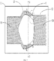
FIG. 2 is a schematic top view of a bulk acoustic wave resonator according to an exemplary embodiment of the present disclosure. - In the embodiment shown in
FIG. 2 ,reference numeral 10 represents a bottom electrode of the resonator, and the bottom electrode is connected with four sides of a pentagon (defined as an effective region) of the resonator;reference numeral 11 represents a piezoelectric layer of the resonator;reference numeral 12 represents a top electrode of the resonator;reference numeral 13 represents a bottom electrode metal connection layer above the bottom electrode of the resonator; andreference numeral 14 represents a top electrode metal connection layer above the top electrode of the resonator. Portions of the bottom electrode metal connection layer surrounding edge portions of the effective region have widths d1 and d2. Values of d1 and d2 may be equal or unequal to each other, generally are in a range of 1-50 µm, and typically are in a range of 5-10 µm, and may also be 20 µm or 7 µm except for end values of the above ranges. The bottom electrode metal connection layer and the top electrode metal connection layer each have a thickness which is generally in a range of 100 nm to 5 µm, and may also be for example 1 µm except for the end values of the above ranges. - In this embodiment, as shown in
FIG. 2 , the four sides of the pentagon of the resonator are connected with the bottom electrode metal connection layer. Accordingly, when a voltage is applied to the bottom electrode of the resonator, a same potential is generated across the four sides a, b, c, and d of the pentagon of the resonator connected with the bottom electrode due to an extremely high conductivity of the bottom electrode metal connection layer. A current flows in from four sides of the bottom electrode. Thus, when the resonator operates, its resistance Rs (series resistance) is decreased, i.e., an electrical energy loss of the electrodes is reduced, so that a Q value of the resonator is improved and an IL value (insertion loss value) of the filter, which is composed of the electrodes, are also improved. Meanwhile, since the edges of the effective region of the resonator has the same potential, a main acoustic resonance mode is superior such that a parasitic mode is suppressed from being generated. On the contrary, the potentials of edges of the effective region of the conventional resonator are different from each other, resulting in inconsistent vibration of each part of the resonator, and thus the parasitic mode is enhanced. - Further, since the bottom electrode metal connection layer located above the bottom electrode also uniformly covers the periphery of the pentagon of the resonator and the metal has good heat dissipation performance, a thermal resistance in the resonator is effectively reduced. Accordingly, a power capacity of the resonator is improved.
-
FIG. 3 is a schematic exemplary partial enlarged view of part A (where an end of the top electrode is adjacent to an end of the bottom electrode) inFIG. 2 according to an exemplary embodiment of the present disclosure.Reference numeral 10 represents the bottom electrode,reference numeral 12 represents the top electrode,reference numeral 13 represents the bottom electrode metal connection layer above the bottom electrode,reference numeral 14 represents the top electrode metal connection layer above the top electrode, andreference numeral 30 represents a cavity structure at a bottom of the resonator. A distance d3 is formed between the metal connection layers 13 and 14 to avoid a short circuit caused by contact between the top electrode metal connection layer and the bottom electrode metal connection layer, and a value of the distance d3 may be greater than 5 µm. -
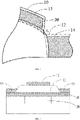
FIG. 4 is a schematic view along line B-B inFIG. 2 according to an exemplary embodiment of the present disclosure. InFIG. 4 , the resonator is sequentially provided with the following elements in a vertical direction: anacoustic mirror structure 30, which may be a cavity structure etched in a substrate or a cavity structure protruding upwardly, or may be in an acoustic wave reflection form such as a Bragg reflection structure, and is the cavity structure etched in the substrate inFIG. 4 ; thebottom electrode 10; thepiezoelectric layer 11; thetop electrode 12; and the bottom electrodemetal connection layer 13 disposed above the bottom electrode, in which portions of the bottom electrode metal connection layer surrounding the edges of the effective region have widths d1 and d2. The values of d1 and d2 may be equal or unequal to each other, generally are in a range of 1-50 µm, and typically are in a range of 5-10 µm, and the bottom electrode metal connection layer generally has a thickness of 100 nm-5 µm. -
FIG. 5 is a schematic view along line B-B inFIG. 2 according to another exemplary embodiment of the present disclosure. The structure shown inFIG. 5 is similar to that shown inFIG. 4 except that the bottom electrode metal connection layer connected with the pentagon of the resonator inFIG. 5 covers a portion of thepiezoelectric layer 11 across steps and is vertically spaced apart from edges of the cavity structure by a spacing d6, a value of which is greater than zero. In this way, a region covered by the metal connection layer is increased, which in turn increases heat dissipation function to effectively reduce the thermal resistance in the resonator. Accordingly, the power capacity of the resonator is further improved. -
FIG. 6 is a schematic view along line B-B inFIG. 2 according to another exemplary embodiment of the present disclosure. The structure shown inFIG. 6 is similar to that shown inFIG. 5 except that a plurality of bumps is arranged on the bottom electrode metal connection layer to further improve the heat dissipation performance and reduce the thermal resistance in the resonator, so that the power capacity of the resonator is further improved. The heat dissipation structure is not limited to the bumps shown inFIG. 6 , and may be a rib structure or other structures facilitating to increase the heat dissipation area. -
FIG. 7 is a schematic top view of a bulk acoustic wave resonator according to an exemplary embodiment of the present disclosure. The structure shown inFIG. 7 is similar to that shown inFIG. 2 , except that the bottom electrodemetal connection layer 13 and the top electrodemetal connection layer 14 only partially cover thebottom electrode 10 and thetop electrode 12. Meanwhile, a portion of the end of thebottom electrode 10 vertically overlaps thetop electrode 12 to increase a mechanical strength of the resonator at corners, so that the structure of the resonator is more stable. -
FIG. 8 is a schematic exemplary partial enlarged view of part C inFIG. 7 according to an exemplary embodiment of the present disclosure, whereinreference numeral 10 represents the bottom electrode,reference numeral 12 represents the top electrode,reference numeral 30 represents the cavity structure,reference numeral 13 represents the bottom electrode metal connection layer above the bottom electrode, andreference numeral 14 represents the top electrode metal connection layer above the top electrode. In this embodiment, the bottom electrode and the top electrode overlap each other in a vertical direction at their boundary connections. In this way, since overlapped potions are located at the corners, the mechanical strength of the resonator at the corners is increased so that the structure of the resonator is more stable. -
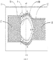
FIG. 9 is a schematic top view of a bulk acoustic wave resonator according to an exemplary embodiment of the present disclosure. The structure shown inFIG. 9 is similar to that shown inFIG. 7 , except that the top electrode of the resonator is connected to the four sides of the pentagon of the resonator. Further, portions of the top electrode metal connection layer arranged above the top electrode surrounds the edges of the pentagon of the resonator and have widths d1 and d2. The values of d1 and d2 may be equal or unequal to each other, generally are in a range of 1-50 µm, and typically are in a range of 5-10 µm, and the top electrode metal connection layer generally has a thickness which is generally in a range of 100 nm to 5 µm. Moreover, abridge structure 100 is provided between an edge of the top electrode and the pentagon of the resonator. The bridge structure spans a boundary of the cavity structure, and has a width d5, which may be typically 5 µm. Since an acoustic impedance of the bridge structure does not match with that in the effective region of the resonator due to an air gap at the bridge structure, an acoustic wave transmission at the boundary is discontinuous. Thus, a part of acoustic energy at the boundary will be coupled and reflected to an effective excitation region and is then converted into a piston acoustic wave mode perpendicular to a surface of the piezoelectric layer, so that a Q factor of the resonator is improved. -
FIG. 10 is a schematic exemplary enlarged partial view of part D inFIG. 9 according to an exemplary embodiment of the present disclosure.Reference numeral 10 represents the bottom electrode,reference numeral 12 represents the top electrode,reference numeral 30 represents the cavity structure,reference numeral 13 represents the bottom electrode metal connection layer above the bottom electrode,reference numeral 14 represents the top electrode metal connection layer above the top electrode, andreference numeral 100 represents the bridge structure. In this embodiment, since the bridge structure is formed between the edge of the top electrode and the edges of the pentagon of the resonator, the acoustic wave energy in the resonator is limited within its effective region such that the Q value of the resonator is improved. -
FIG. 11 is a schematic view along line B-B inFIG. 9 according to an exemplary embodiment of the present disclosure. InFIG. 11 , the resonator is sequentially provided with the following elements in the vertical direction: theacoustic mirror structure 30, which may be a cavity structure etched in the substrate or a cavity structure protruding upwardly, or may be in an acoustic wave reflection form such as a Bragg reflection structure, and is the cavity structure etched in the substrate inFIG. 12 ; thebottom electrode 10; thepiezoelectric layer 11; thetop electrode 12; thebridge structure 100; theair gap 101 located between the bridge structure and the piezoelectric layer; and the top electrodemetal connection layer 14. Portions of the top electrode metal connection layer surrounding the edges of the pentagon have widths d1 and d2, of which the values may be equal or unequal to each other, generally are in a range of 1-50 µm, and typically is in a range of 5-10 µm, and the top electrode metal connection layer has a thickness of 100 nm-5 µm. - It should be noted that, although not shown, the top electrode may not be provided with the bridge structure, and the top electrode metal connection layer is directly connected to the edges of the top electrode.
-
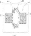
FIG. 12 is a schematic top view of a bulk acoustic wave resonator according to an exemplary embodiment of the present disclosure. The structure shown inFIG. 12 is similar to that shown inFIG. 9 , except that the bottom and top electrodes of the resonator are both connected to the sides of the pentagon of the resonator, and the edges of the top electrode metal connection layer located above the bottom and top electrodes are spaced apart from the sides of the pentagon by spacings d1 and d2, respectively. The values of d1 and d2 may be equal or unequal to each other, generally are in a range of 1-50 µm, and typically are in a range of 5-10 µm, and the top electrode metal connection layer generally has a thickness of 100 nm-5 µm. - In the present disclosure, the top electrode metal connection layer or the bottom electrode metal connection layer is arranged around 50% or more of a peripheral length of the effective region, or the two metal connection layers are arranged around 50% or more of the peripheral length of the effective region in total.
- It should be noted that, in the exemplary embodiment of the present disclosure, the effective region of the pentagonal shape is described as an example. However, the present disclosure is not limited thereto, and the effective region may also be in other shapes.
- In the present disclosure, it can be understood that the metal connection layer may include a base connection portion (e.g., a
base connection portion 13A of the bottom electrodemetal connection layer 13 inFIG. 2 ) and a surrounding portion extending around the effective region from a side of the base connection portion (for example, the surroundingportion 13A of the bottom electrode metal connection layer inFIG. 2 ). Obviously, the surrounding portion may be disposed at either side or both sides of the base connection portion. - In the present disclosure, the electrode metal connection layers may be made of gold(Au), aluminum(Al), copper(Cu), silver(Ag), or similar materials with good conductivity. The top electrode and the bottom electrode may be made of Tungsten(W), molybdenum(Mo), platinum(Pt), ruthenium(Ru), iridium(Ir), titanium tungsten(TiW), aluminum(Al), titanium(Ti), and other similar metals. The piezoelectric layer material may be made of aluminum nitride(AlN), zinc oxide(ZnO), lead zirconate titanate(PZT), lithium niobate(LiNbO3), quartz(Quartz), potassium niobate (KNbO3) or lithium tantalate(LiTaO3), or other similar materials.
- In view of the above description, there is provided a bulk acoustic wave resonator, including:
- a substrate;
- an acoustic mirror;
- a bottom electrode provided above the substrate and having a bottom electrode metal connection layer;
- a top electrode arranged opposite to the bottom electrode and having a top electrode metal connection layer; and
- a piezoelectric layer provided above the bottom electrode and arranged between the bottom electrode and the top electrode,
- wherein:
- the acoustic mirror, the bottom electrode, the piezoelectric layer and the top electrode overlap each other in a thickness direction of the resonator to form an overlapping region which is defined as an effective region of the resonator; and
- the top electrode metal connection layer and the bottom electrode metal connection layer are arranged around 50% or more of a peripheral length of the effective region in total.
- It should be noted that, in the present disclosure, "the top electrode metal connection layer and the bottom electrode metal connection layer are arranged around...in total" includes a situation where the metal connection layers are both arranged partially around the effective region (for example, see
FIG. 12 ), a situation where one of the metal connection layers only extends towards but not around the effective region and the other metal connection layer is arranged around the effective region (for example, seeFIG. 2 where the top electrode metal connection layer may be shown to have a smaller width), and a situation where one of the metal connection layers does not extend near the effective region (for example, the bottom electrode metal connection layer shown inFIG. 1 ) and the other metal connection layer is arranged around the effective region. - Further, one of the top electrode metal connection layer and the bottom electrode metal connection layer is arranged around 90% or more of the peripheral length of the effective region.
- Further, the top electrode metal connection layer or the bottom electrode metal connection layer is arranged around 50% or more of the peripheral length of the effective region.
- Further, a portion of the top electrode metal connection layer and/or the bottom electrode metal connection layer surrounding the effective region has a width which is in a range of 1-50 µm.
- In addition, there is also provided a bulk acoustic wave resonator, including:
- a substrate;
- an acoustic mirror;
- a bottom electrode provided above the substrate and having a bottom electrode metal connection layer;
- a top electrode arranged opposite to the bottom electrode and having a top electrode metal connection layer; and
- a piezoelectric layer provided above the bottom electrode and arranged between the bottom electrode and the top electrode,
- wherein:
- the acoustic mirror, the bottom electrode, the piezoelectric layer and the top electrode overlap each other in a thickness direction of the resonator to form an overlapping region which is defined as an effective region of the resonator;
- at least one of the top electrode metal connection layer and the bottom electrode metal connection layer has a base connection portion and a surrounding portion extending around at least part of the effective region from either side or both sides of the base connection portion. Alternatively, the surrounding portion is arranged around 50% or more of a peripheral length of the effective region. Alternatively, the surrounding portion has a width which is in a range of 1-50 µm. Further, the width of the surrounding portion is in a range of 5-10 µm.
- Based on the above, the present disclosure further provides a filter including a plurality of the bulk acoustic wave resonators as described above. The present disclosure also provides an electronic device including the filter or the bulk acoustic wave resonator as described above.
- Although the embodiments of the present disclosure have been shown and described, it can be understood for those skilled in the art that modifications can be made to these embodiments without departing from the principle and spirit of the present disclosure, and the scope of the present disclosure is defined by the appended claims and their equivalents.
Claims (28)
- A bulk acoustic wave resonator, comprising:a substrate;an acoustic mirror;a bottom electrode provided above the substrate and having a bottom electrode metal connection layer;a top electrode arranged opposite to the bottom electrode and having a top electrode metal connection layer; anda piezoelectric layer provided above the bottom electrode and arranged between the bottom electrode and the top electrode,characterized in that,the acoustic mirror, the bottom electrode, the piezoelectric layer and the top electrode overlap each other in a thickness direction of the resonator to form an overlapping region, and the overlapping region is defined as an effective region of the resonator; andthe top electrode metal connection layer and the bottom electrode metal connection layer are arranged around 50% or more of a peripheral length of the effective region in total.
- The resonator according to claim 1, characterized in that the bottom electrode metal connection layer is arranged around at least a portion of the piezoelectric layer corresponding to the effective region.
- The resonator according to claim 2, characterized in that a thickness of the bottom electrode metal connection layer is the same as a thickness of the piezoelectric layer.
- The resonator according to claim 2, characterized in that the bottom electrode metal connection layer is provided with a first portion arranged on the bottom electrode and a second portion covering a part of an upper surface of the piezoelectric layer, and the second portion is spaced apart from the top electrode.
- The resonator according to claim 4, characterized in that the first portion is provided with a heat dissipation structure.
- The resonator according to claim 4, characterized in that in a projection in the thickness direction of the resonator, the second portion and the top electrode are spaced apart from each other by a first distance.
- The resonator according to claim 4, characterized in that in a projection in the thickness direction of the resonator, the second portion is located at an outer side of an edge of the acoustic mirror, and is spaced apart from the edge of the acoustic mirror by a second distance (d6).
- The resonator according to claim 1, characterized in that the top electrode metal connection layer and the bottom electrode metal connection layer are arranged around 90% or more of the peripheral length of the effective region in total.
- The resonator according to claim 1, characterized in that the top electrode metal connection layer or the bottom electrode metal connection layer is arranged around 50% or more of the peripheral length of the effective region.
- The resonator according to claim 1, characterized in that a portion of the top electrode metal connection layer surrounding the effective region and/or a portion of the bottom electrode metal connection layer surrounding the effective region has a width in a range of 1-50 µm.
- The resonator according to claim 10, characterized in that the width of the portion of the top electrode metal connection layer surrounding the effective region and/or the width of the portion of the bottom electrode metal connection layer surrounding the effective region is in a range of 5-10 µm.
- The resonator according to any one of claims 1 to 11, characterized in that the top electrode metal connection layer is arranged around at least part of the effective region and is connected with the piezoelectric layer.
- The resonator according to any one of claims 1 to 11, characterized in that the top electrode metal connection layer is arranged around at least part of the effective region and is connected with the top electrode.
- The resonator according to claim 13, characterized in that the top electrode is provided with a bridge structure surrounding at least part of the effective region; and
the top electrode metal connection layer surrounds at least part of the bridge structure and is electrically connected to the bridge structure. - The resonator according to claim 14, characterized in that the top electrode metal connection layer is electrically connected to an outer edge of the bridge structure on an upper surface of the outer edge of the bridge structure.
- The resonator according to any one of claims 1 to 15, characterized in that the effective region has a polygonal shape.
- The resonator according to claim 16, characterized in that the at least one of the top electrode metal connection layer and the bottom electrode metal connection layer arranged around at least part of the effective region comprises one of the top electrode metal connection layer and the bottom electrode metal connection layer arranged around at least half of an edge of the effective region.
- The resonator according to claim 17, characterized in that the polygonal shape comprises a pentagonal shape; and
the at least one of the top electrode metal connection layer and the bottom electrode metal connection layer arranged around at least part of the effective region comprises one of the top electrode metal connection layer and the bottom electrode metal connection layer arranged substantially around at least three continuous sides of the polygonal shape. - The resonator according to claim 18, characterized in that the top electrode metal connection layer is arranged around four sides of the pentagonal shape, and the bottom electrode metal connection layer is arranged around the remaining side of the pentagonal shape; orthe bottom electrode metal connection layer is arranged around four sides of the pentagonal shape, and the top electrode metal connection layer is arranged around the remaining side of the pentagonal shape; orthe bottom electrode metal connection layer is arranged around substantially one half of an edge of the pentagonal shape, and the top electrode metal connection layer is arranged around another half of the edge of the pentagonal shape.
- The resonator according to any one of claims 1 to 19, characterized in that an end of the top electrode and an end of the bottom electrode partially overlap each other in a projection thereof in the thickness direction of the resonator.
- The resonator according to any one of claims 1 to 19, characterized in that an end of the top electrode and an end of the bottom electrode are spaced apart from each other by a third distance (d3) in a projection thereof in the thickness direction of the resonator.
- The resonator according to claim 21, characterized in that the third distance is greater than 5 µm.
- A bulk acoustic wave resonator, comprising:a substrate;an acoustic mirror;a bottom electrode provided above the substrate and having a bottom electrode metal connection layer;a top electrode arranged opposite to the bottom electrode and having a top electrode metal connection layer; anda piezoelectric layer provided above the bottom electrode and arranged between the bottom electrode and the top electrode,characterized in that,the acoustic mirror, the bottom electrode, the piezoelectric layer and the top electrode overlap each other in a thickness direction of the resonator to form an overlapping region which is defined as an effective region of the resonator; andat least one of the top electrode metal connection layer and the bottom electrode metal connection layer has a base connection portion and a surrounding portion, and the surrounding portion extends around at least part of the effective region from either sides or both sides of the base connection portion.
- The resonator according to claim 23, characterized in that the surrounding portion is arranged around 50% or more of a peripheral length of the effective region.
- The resonator according to claim 23, characterized in that the surrounding portion has a width in a range of 1-50 µm.
- The resonator according to claim 25, characterized in that the width of the surrounding portion is in a range of 5-10 µm.
- A filter comprising the bulk acoustic wave resonator according to any one of claims 1 to 26.
- An electronic device comprising the filter according to claim 27 or the bulk acoustic wave resonator according to any one of claims 1 to 26.
Applications Claiming Priority (2)
| Application Number | Priority Date | Filing Date | Title |
|---|---|---|---|
| CN201910610938.8A CN111010132A (en) | 2019-07-08 | 2019-07-08 | BAW resonators, filters and electronic equipment |
| PCT/CN2020/086558 WO2021004127A1 (en) | 2019-07-08 | 2020-04-24 | Bulk acoustic resonator, filter, and electronic device |
Publications (2)
| Publication Number | Publication Date |
|---|---|
| EP3998704A1 true EP3998704A1 (en) | 2022-05-18 |
| EP3998704A4 EP3998704A4 (en) | 2022-09-28 |
Family
ID=70111450
Family Applications (1)
| Application Number | Title | Priority Date | Filing Date |
|---|---|---|---|
| EP20836329.1A Pending EP3998704A4 (en) | 2019-07-08 | 2020-04-24 | ACOUSTIC RESONATOR IN VOLUME, FILTER AND ELECTRONIC DEVICE |
Country Status (3)
| Country | Link |
|---|---|
| EP (1) | EP3998704A4 (en) |
| CN (1) | CN111010132A (en) |
| WO (1) | WO2021004127A1 (en) |
Families Citing this family (6)
| Publication number | Priority date | Publication date | Assignee | Title |
|---|---|---|---|---|
| CN111010132A (en) * | 2019-07-08 | 2020-04-14 | 天津大学 | BAW resonators, filters and electronic equipment |
| CN111654261B (en) * | 2020-04-21 | 2021-08-10 | 诺思(天津)微系统有限责任公司 | Bulk acoustic wave resonator, method of designing bulk acoustic wave resonator, filter, and electronic apparatus |
| CN114070233A (en) * | 2020-08-04 | 2022-02-18 | 诺思(天津)微系统有限责任公司 | Bulk Acoustic Resonators, Filters, and Electronics for Spurious Mode Reduction |
| CN114553178B (en) * | 2020-11-24 | 2025-10-17 | 诺思(天津)微系统有限责任公司 | Bulk acoustic resonator with tungsten electrode, filter and electronic equipment |
| WO2024087049A1 (en) * | 2022-10-26 | 2024-05-02 | 京东方科技集团股份有限公司 | Bulk acoustic wave resonator and electronic device |
| CN115498975A (en) * | 2022-11-16 | 2022-12-20 | 迈感微电子(上海)有限公司 | Film bulk acoustic resonator and filter |
Family Cites Families (14)
| Publication number | Priority date | Publication date | Assignee | Title |
|---|---|---|---|---|
| JP3879643B2 (en) * | 2002-09-25 | 2007-02-14 | 株式会社村田製作所 | Piezoelectric resonator, piezoelectric filter, communication device |
| JP4550658B2 (en) * | 2005-04-28 | 2010-09-22 | 富士通メディアデバイス株式会社 | Piezoelectric thin film resonator and filter |
| JP2007208728A (en) * | 2006-02-02 | 2007-08-16 | Fujitsu Media Device Kk | Piezoelectric thin film resonator, filter and manufacturing method thereof |
| JP5191762B2 (en) * | 2008-03-06 | 2013-05-08 | 太陽誘電株式会社 | Piezoelectric thin film resonator, filter, and communication device |
| US9203374B2 (en) * | 2011-02-28 | 2015-12-01 | Avago Technologies General Ip (Singapore) Pte. Ltd. | Film bulk acoustic resonator comprising a bridge |
| US9490770B2 (en) * | 2011-03-29 | 2016-11-08 | Avago Technologies General Ip (Singapore) Pte. Ltd. | Acoustic resonator comprising temperature compensating layer and perimeter distributed bragg reflector |
| JP5918522B2 (en) * | 2011-12-12 | 2016-05-18 | 太陽誘電株式会社 | Filters and duplexers |
| KR101928359B1 (en) * | 2012-09-11 | 2018-12-12 | 삼성전자주식회사 | Resonance apparatus for processing electric loss using conductive material and the method for manufacturing reasonator |
| US10804877B2 (en) * | 2014-01-21 | 2020-10-13 | Avago Technologies International Sales Pte. Limited | Film bulk acoustic wave resonator (FBAR) having stress-relief |
| US9853626B2 (en) * | 2014-03-31 | 2017-12-26 | Avago Technologies General Ip (Singapore) Pte. Ltd. | Acoustic resonator comprising acoustic redistribution layers and lateral features |
| KR102052795B1 (en) * | 2017-03-23 | 2019-12-09 | 삼성전기주식회사 | Acoustic resonator |
| US11418168B2 (en) * | 2017-05-30 | 2022-08-16 | Samsung Electro-Mechanics Co., Ltd. | Acoustic resonator and method for manufacturing the same |
| US11563417B2 (en) * | 2017-11-20 | 2023-01-24 | Samsung Electro-Mechanics Co., Ltd. | Acoustic resonator |
| CN111010132A (en) * | 2019-07-08 | 2020-04-14 | 天津大学 | BAW resonators, filters and electronic equipment |
-
2019
- 2019-07-08 CN CN201910610938.8A patent/CN111010132A/en active Pending
-
2020
- 2020-04-24 WO PCT/CN2020/086558 patent/WO2021004127A1/en not_active Ceased
- 2020-04-24 EP EP20836329.1A patent/EP3998704A4/en active Pending
Also Published As
| Publication number | Publication date |
|---|---|
| CN111010132A (en) | 2020-04-14 |
| WO2021004127A1 (en) | 2021-01-14 |
| EP3998704A4 (en) | 2022-09-28 |
Similar Documents
| Publication | Publication Date | Title |
|---|---|---|
| CN111010123B (en) | Bulk acoustic wave resonator, filter, and electronic device having electrode with void layer and protrusion structure | |
| US10727808B2 (en) | Bulk acoustic wave resonator comprising a ring | |
| US12324355B2 (en) | Acoustic wave device | |
| US7649304B2 (en) | Piezoelectric resonator and piezoelectric filter | |
| CN111010132A (en) | BAW resonators, filters and electronic equipment | |
| JP4963379B2 (en) | Performance enhancement of acoustic resonators using alternating edge structures | |
| CN113572448B (en) | Bulk acoustic wave resonator | |
| KR20220044383A (en) | seismic device | |
| EP1406386B1 (en) | Piezoelectric resonator, piezoelectric filter, and communication apparatus | |
| US20100134210A1 (en) | Piezoelectric Resonator and Piezoelectric Filter Device | |
| US20220216845A1 (en) | Acoustic wave device | |
| CN111010111B (en) | Bulk acoustic wave resonator, filter and electronic device with additional structure separated from top electrode | |
| CN111193485A (en) | BAW resonators, filters and electronics with rough surfaces | |
| EP4027519A1 (en) | Bulk acoustic wave resonator and manufacturing method therefor, filter and electronic device | |
| CN111010130A (en) | Bulk acoustic wave resonator with temperature compensation layer and electrical layer, filter and electronic equipment | |
| CN111082776B (en) | Bulk acoustic wave resonator, filter and electronic device with electrode with void layer | |
| US12255628B2 (en) | Acoustic wave device | |
| CN111010121A (en) | Bulk acoustic wave resonator with non-conductive insertion layer, filter and electronic device | |
| JP2004120016A (en) | Filter device | |
| JP2014135568A (en) | Piezoelectric thin film resonator and filter | |
| CN111193482A (en) | Bulk acoustic wave resonator with fracture structure, method of manufacturing the same, filter, and electronic apparatus | |
| CN118285056A (en) | Elastic wave device | |
| JP2005311849A (en) | Piezoelectric thin film resonator, filter, and method of manufacturing piezoelectric thin film resonator | |
| CN115225050A (en) | Method for resonator fabrication, bulk acoustic wave resonator | |
| US12562709B2 (en) | Acoustic wave device |
Legal Events
| Date | Code | Title | Description |
|---|---|---|---|
| STAA | Information on the status of an ep patent application or granted ep patent |
Free format text: STATUS: THE INTERNATIONAL PUBLICATION HAS BEEN MADE |
|
| PUAI | Public reference made under article 153(3) epc to a published international application that has entered the european phase |
Free format text: ORIGINAL CODE: 0009012 |
|
| STAA | Information on the status of an ep patent application or granted ep patent |
Free format text: STATUS: REQUEST FOR EXAMINATION WAS MADE |
|
| 17P | Request for examination filed |
Effective date: 20220207 |
|
| AK | Designated contracting states |
Kind code of ref document: A1 Designated state(s): AL AT BE BG CH CY CZ DE DK EE ES FI FR GB GR HR HU IE IS IT LI LT LU LV MC MK MT NL NO PL PT RO RS SE SI SK SM TR |
|
| REG | Reference to a national code |
Ref country code: DE Ref legal event code: R079 Free format text: PREVIOUS MAIN CLASS: H03H0009170000 Ipc: H03H0009020000 |
|
| A4 | Supplementary search report drawn up and despatched |
Effective date: 20220825 |
|
| RIC1 | Information provided on ipc code assigned before grant |
Ipc: H03H 9/17 20060101ALI20220819BHEP Ipc: H03H 9/13 20060101ALI20220819BHEP Ipc: H03H 9/02 20060101AFI20220819BHEP |
|
| DAV | Request for validation of the european patent (deleted) | ||
| DAX | Request for extension of the european patent (deleted) | ||
| STAA | Information on the status of an ep patent application or granted ep patent |
Free format text: STATUS: EXAMINATION IS IN PROGRESS |
|
| 17Q | First examination report despatched |
Effective date: 20251120 |